19
© 3M 2007. All Rights Reserved. Modeling Techniques for Evaluation of RFID Tag Antennas In Situ Riki Banerjee 3M Company

© 3M 2007. All Rights Reserved.
Modeling Techniques for Evaluation of
RFID Tag Antennas In Situ
Riki Banerjee
3M Company

Outline
� RFID operation
� RFID tag design
� Evaluation techniques In Situ
� Conclusions
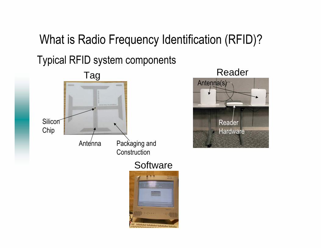
What is Radio Frequency Identification (RFID)?
Typical RFID system components
Tag
Antenna
Silicon
Chip
Packaging and
Construction
ReaderAntenna(s)
Reader
Hardware
Software

Different Types of RFID Tags

Various Readers
Handhelds Portals Reader Pads
Standard readers can be configured for the application.

Common Frequencies of RFID
0.12 m2.45 GHz
0.33 m915 MHz
22.1 m13.56 MHz
2400 m125 kHz
Wavelength (λ)Frequency
Antennas less than λ/10 predominately only have
stationary fields.
Antennas greater than λ/10 create stationary and significant radiated
fields.
Radiated fields create longer read range.
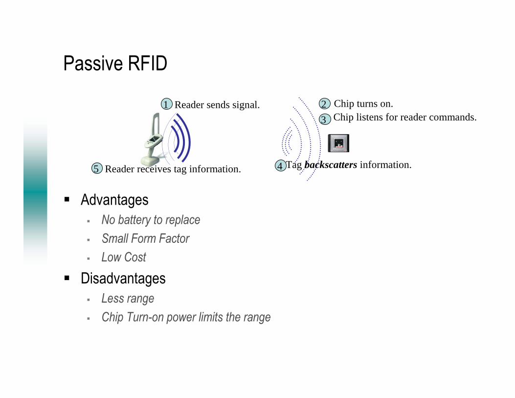
Passive RFID
� Advantages
� No battery to replace
� Small Form Factor
� Low Cost
� Disadvantages
� Less range
� Chip Turn-on power limits the range
2 Chip turns on.
3 Chip listens for reader commands.1 Reader sends signal.
Tag backscatters information.45 Reader receives tag information.

Passive RFID Summary
What affects performance?
� Providing enough signal to turn on tag chip� Reader power and antenna size
� Reader-to-tag distance
� Tag antenna size and chip turn-on voltage
� Orientation of reader and tag antennas
� Presence of objects in close proximity to tag
� Speed of movement of tag in and out of reader fields
� Propagation medium between reader and tag
Advantages
� No battery to
replace
� Small Form Factor
� Low Cost
Disadvantages
� Less range
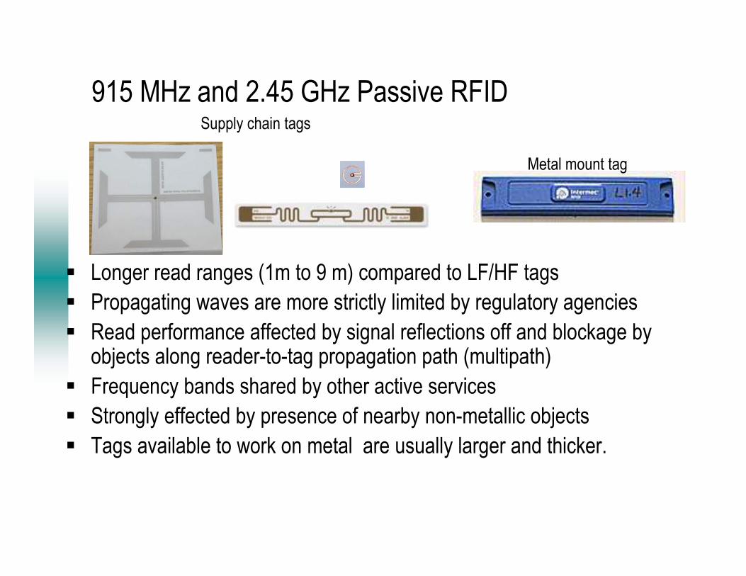
915 MHz and 2.45 GHz Passive RFID
� Longer read ranges (1m to 9 m) compared to LF/HF tags
� Propagating waves are more strictly limited by regulatory agencies
� Read performance affected by signal reflections off and blockage by objects along reader-to-tag propagation path (multipath)
� Frequency bands shared by other active services
� Strongly effected by presence of nearby non-metallic objects
� Tags available to work on metal are usually larger and thicker.
Metal mount tag
Supply chain tags
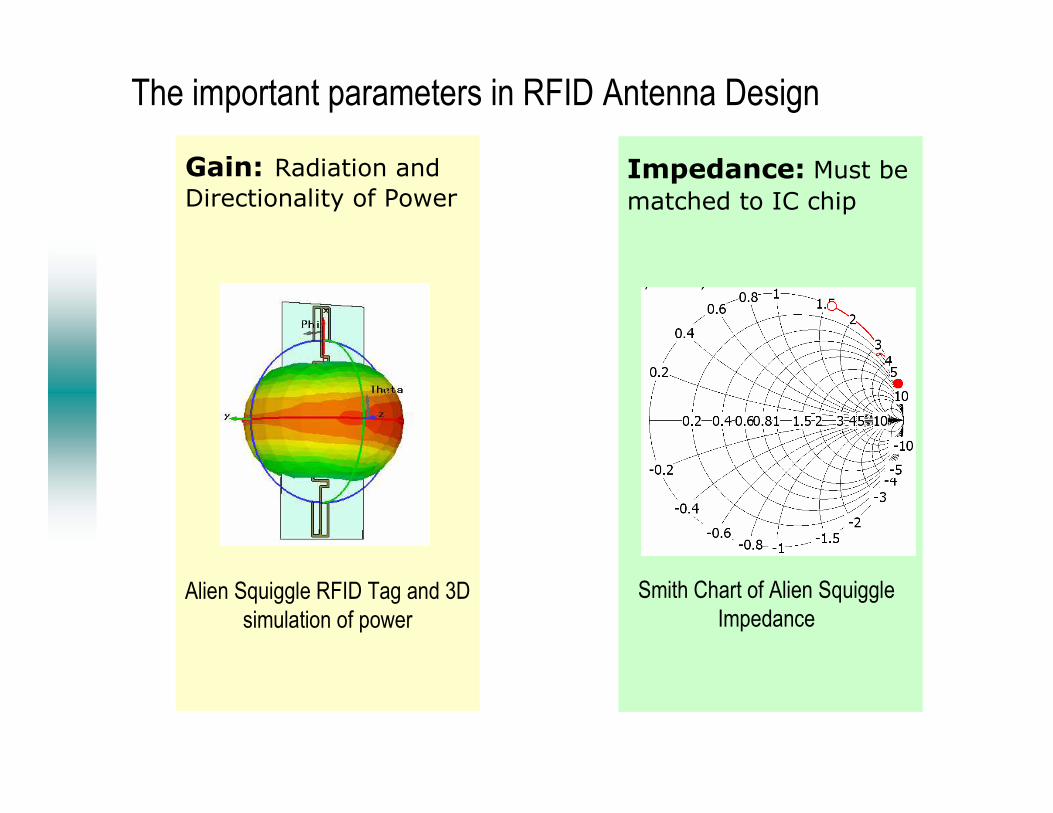
The important parameters in RFID Antenna Design
Gain: Radiation and Directionality of Power
Alien Squiggle RFID Tag and 3D
simulation of power
Smith Chart of Alien Squiggle
Impedance
Impedance: Must be matched to IC chip

915 MHz RFID Tag Design
� Chips are inexpensive (no on-chip matching), therefore very
capacitive.
� Antenna must be designed to provide the conjugate match.
� Traditional 50 ohm antenna designs are not used for RFID.
� Design is done using CST Microwave Studio – Transient Solver
Open (add space)
boundary conditions.
50 ohm discrete S-parameter port

915 MHz RFID Tag Parameters
Gain of the Tag
Impedance of the tag is inductive.

Assessing Tag Bandwidth
Can be done using CST Design Studio.
1
cap pFcap pF
1
Chip impedance is inserted at the port.
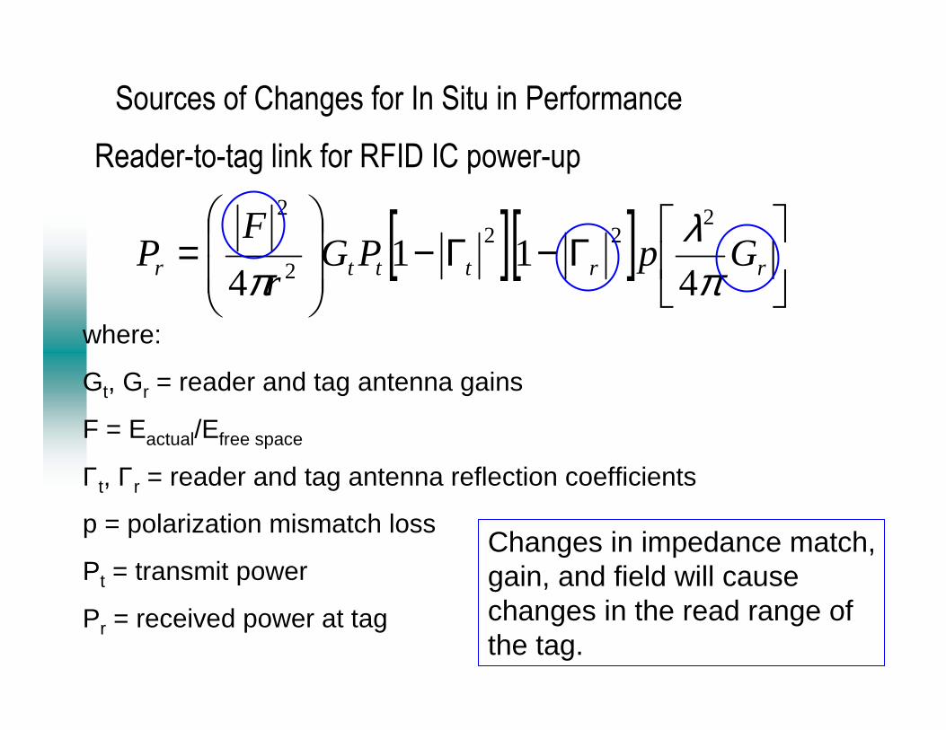
Sources of Changes for In Situ in Performance
Reader-to-tag link for RFID IC power-up
[ ][ ]
Γ−Γ−
= rrtttr GpPG
r
FP
πλ
π 411
4
222
2
2
where:
Gt, Gr = reader and tag antenna gains
F = Eactual/Efree space
Γt, Γr = reader and tag antenna reflection coefficients
p = polarization mismatch loss
Pt = transmit power
Pr = received power at tag
Changes in impedance match, gain, and field will cause changes in the read range of the tag.

Impedance/Gain Change: Tag within in an item
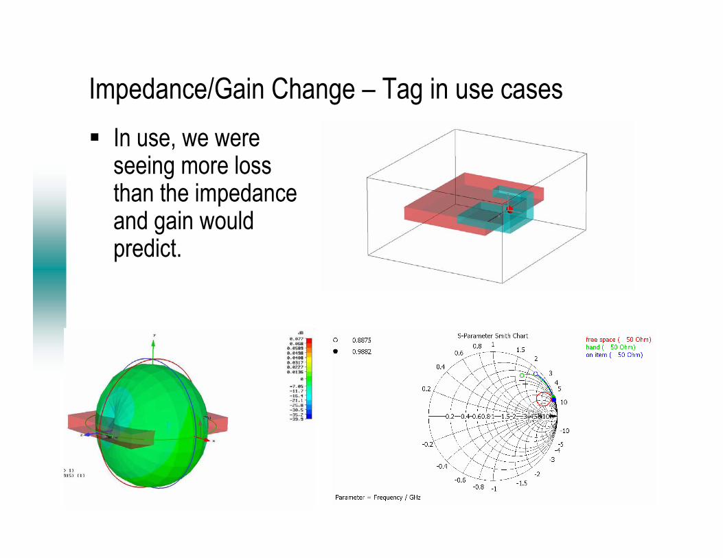
Impedance/Gain Change – Tag in use cases
� In use, we were seeing more loss than the impedance and gain would predict.

Evaluating Problems due to Absorption
� Load tag with chip impedance
� Hit structure with a plane wave.
� Evaluate voltage seen at the load.
The hand alone caused 2 dB of loss.

Evaluating Problems due to Absorption
� Load tag with chip impedance
� Hit structure with a plane wave.
� Evaluate voltage seen at the load.
The addition of other body parts caused 9.7 dB of loss.
A 10 dB decrease in field will result in a 70% decrease in read range.

Conclusions
� Modeling can be used to parse out the detailed affects
of changes in performance.
� RFID tags are expected to perform in complex
environments under complex conditions.
� Modeling can demonstrate feasibility and assist with
improvements in the design.


