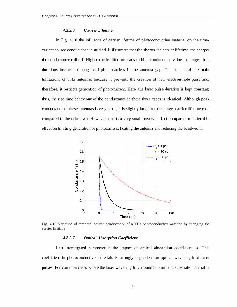
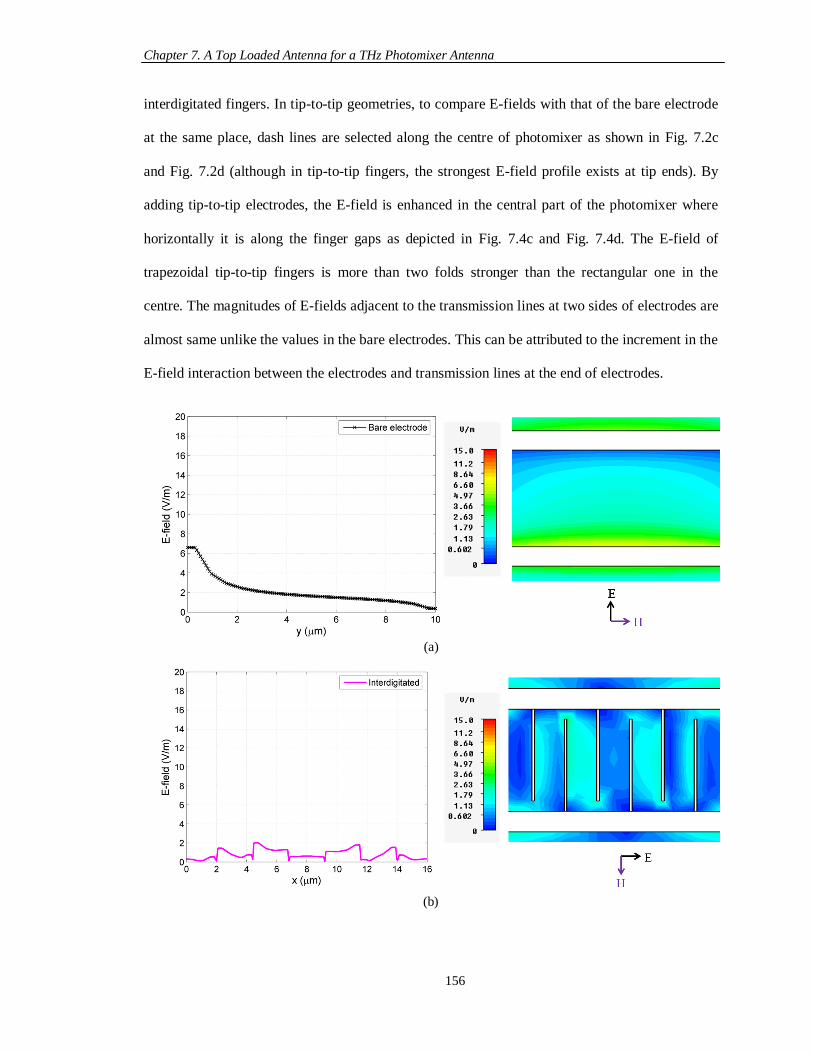
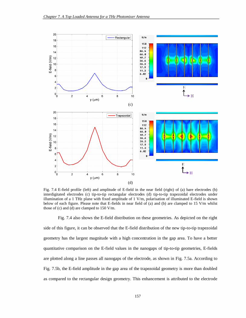
Modelling, Design and Characterisation of Terahertz Photoconductive Antennas by Neda Khiabani Submitted in accordance with the requirements for the award of the degree of Doctor of Philosophy of the University of Liverpool September 2013
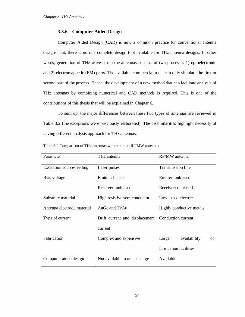
Transcript
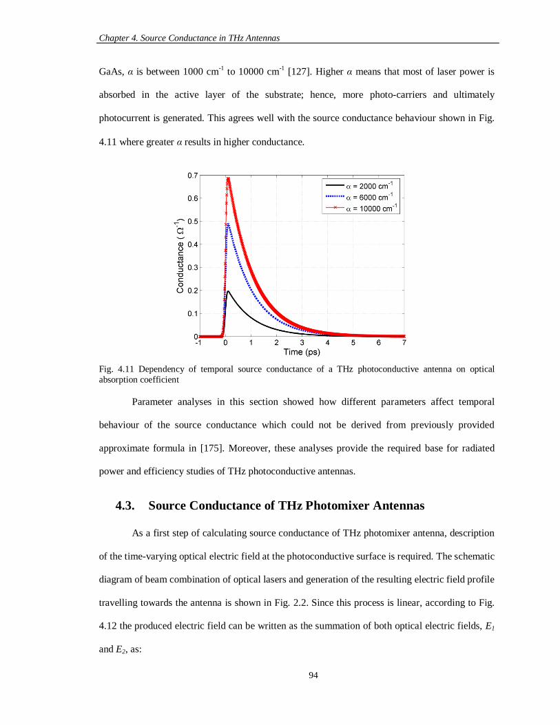
Modelling, Design and Characterisation of
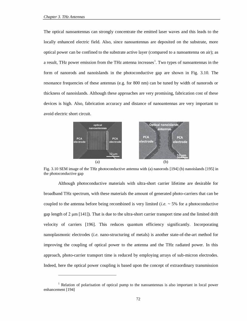
Terahertz Photoconductive Antennas
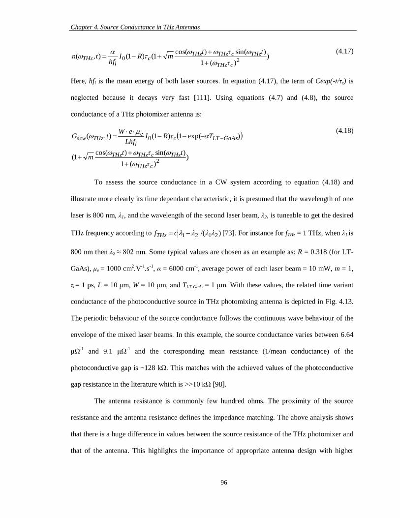
by
Neda Khiabani
Submitted in accordance with the requirements for the award of the degree of Doctor of
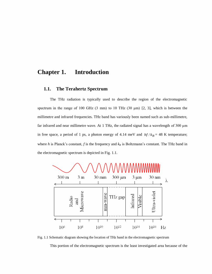
The THz radiation is typically used to describe the region of the electromagnetic
spectrum in the range of 100 GHz (3 mm) to 10 THz (30 μm) [2, 3], which is between the
millimetre and infrared frequencies. THz band has variously been named such as sub-millimetre,
far infrared and near millimetre wave. At 1 THz, the radiated signal has a wavelength of 300 μm
in free space, a period of 1 ps, a photon energy of 4.14 meV and Bkhf / = 48 K temperature;
where h is Planck’s constant, f is the frequency and kB is Boltzmann’s constant. The THz band in
the electromagnetic spectrum is depicted in Fig. 1.1.
Fig. 1.1 Schematic diagram showing the location of THz band in the electromagnetic spectrum
This portion of the electromagnetic spectrum is the least investigated area because of the
Chapter 1. Introduction
2
absence of efficient, coherent, and compact THz sources and detectors [3, 4]. These
characteristics for the sources can be found in the common microwave-frequency sources such as
transistors or RF/MW antennas, and in devices working in the visible and infrared range like
semiconductor laser diodes [5]. However, it is not possible to adopt these technologies for
operation in THz region without a significant reduction in power and efficiency. At the lower
extreme of THz frequency range, the generated power by solid-state electronic devices, such as
diodes, has roll-offs of 1/ f 2 [6] due to reactive-resistive effects and long transit times. On the
other hand, optical devices, such as diode lasers, do not perform well at THz range limit because
of the lack of materials with adequately small bandgap energies [5]. Hence the term “THz gap” is
phrased to explain the infancy of this band as compared to well-developed neighbouring spectral
regions. Recent advances have commenced to address this problem, and various types of new
emitters and detectors based on semiconductor technology are emerging [4, 7-9].
In this chapter, first, different THz sources and detectors are reviewed and evaluated.
Then, THz wave properties and potential applications are described. Based on the built
foundation, the research motivations and objectives of this thesis are outlined.
1.2. THz Sources
The THz source has been considered the most difficult component to realise among all
the elements in this technology [10]. A great deal of effort has been put to extend RF/MW and
optical technologies to THz band, and even combine them in order to realise THz sources with
better performance [11]. Thus, THz emitters are divided into three main groups: THz sources
developed from RF/MW side, THz sources extended from optical side, and THz sources
combining RF/MW and optical techniques. These are now summarised briefly in sequence.
1.2.1. THz Sources from RF/MW Side
In this category, diodes and THz vacuum tube sources are explained.
Chapter 1. Introduction
3
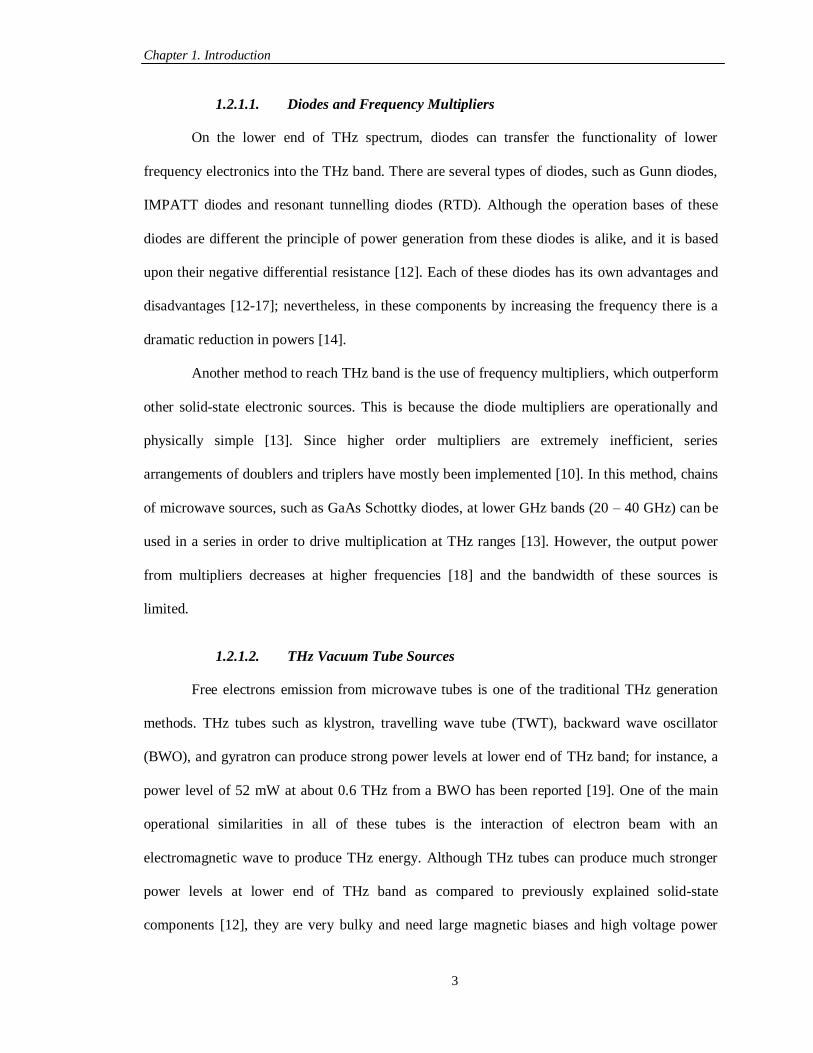
1.2.1.1. Diodes and Frequency Multipliers
On the lower end of THz spectrum, diodes can transfer the functionality of lower
frequency electronics into the THz band. There are several types of diodes, such as Gunn diodes,
IMPATT diodes and resonant tunnelling diodes (RTD). Although the operation bases of these
diodes are different the principle of power generation from these diodes is alike, and it is based
upon their negative differential resistance [12]. Each of these diodes has its own advantages and
disadvantages [12-17]; nevertheless, in these components by increasing the frequency there is a
dramatic reduction in powers [14].
Another method to reach THz band is the use of frequency multipliers, which outperform
other solid-state electronic sources. This is because the diode multipliers are operationally and
physically simple [13]. Since higher order multipliers are extremely inefficient, series
arrangements of doublers and triplers have mostly been implemented [10]. In this method, chains
of microwave sources, such as GaAs Schottky diodes, at lower GHz bands (20 – 40 GHz) can be
used in a series in order to drive multiplication at THz ranges [13]. However, the output power
from multipliers decreases at higher frequencies [18] and the bandwidth of these sources is
limited.
1.2.1.2. THz Vacuum Tube Sources
Free electrons emission from microwave tubes is one of the traditional THz generation
methods. THz tubes such as klystron, travelling wave tube (TWT), backward wave oscillator
(BWO), and gyratron can produce strong power levels at lower end of THz band; for instance, a
power level of 52 mW at about 0.6 THz from a BWO has been reported [19]. One of the main
operational similarities in all of these tubes is the interaction of electron beam with an
electromagnetic wave to produce THz energy. Although THz tubes can produce much stronger
power levels at lower end of THz band as compared to previously explained solid-state
components [12], they are very bulky and need large magnetic biases and high voltage power
Chapter 1. Introduction
4
supplies. These restrict the use of these sources in wide operational settings.
1.2.2. THz Sources from Optical Side
THz sources from optical side are mainly divided in to lasers with different generation
techniques and nonlinear crystals.
1.2.2.1. Molecular Lasers
Injection of grating tuned CO2 lasers into low-pressure flowing gas cavities leads to
generation of THz signals with a power level of few ten milliwatts [10]. The frequency of this
THz power depends on the spectral line of gas; for example, a rotational transition of methanol
occurs at 2.522 THz.
1.2.2.2. THz Semiconductor Lasers
Semiconductor diode lasers are very successful and prevalent in the near-infrared and
visible frequency ranges, however; for THz bands materials with suitable band gaps are not
available unless considering artificially engineered materials [5, 20]. Therefore, the concept of
THz Quantum-Cascade lasers (QCL), which are intra-band lasers and require the creation of
quantized sub-bands, was introduced [4]. For this purpose, several few-nm-thick GaAs layers
separated by AlGaAs barriers need to be fabricated. Therefore, proper engineering of the
thickness of the semiconductor layers (or quantum wells) and also choice of the appropriate bias
voltage is required to achieve population inversion. The energy of the system is inversely
proportional to the square of the layers thicknesses; therefore, by narrowing or widening the
quantum wells, series of multi layers of energy can be created. The electron motion from one
miniband to the next, results in an emission of a THz photon at each transition. QCL can operate
in both pulsed and continuous-wave (CW) modes; its operating frequency is controlled by
quantum well design (band gap engineering), and different wavelengths can be achieved in the
same material. QCLs have been one of the most intensive research topics in THz area during the
Chapter 1. Introduction
5
past decade. The survey on different THz QCLs show that the frequency range of these devices
spans from 0.84 THz to 5 THz at various cryogenic working temperatures [21-24] with the peak
optical power as high as about 200 mW at 4.5 THz [5] and the operation temperature as high as
200 K at about 3.2 THz [25]. It is good to add that a THz QCL with power of 8.5 μW at 4 THz
has been demonstrated in room temperature situation [26]. To sum up, QCLs have larger output
power at higher THz frequencies, and as frequency decreases the power reduces considerably.
One of the main limitations of a THz QCL is that for THz operation, it needs cryogenic cooling,
and this restricts operation of a QCL to the laboratory environments.
1.2.2.3. Optical Down Converters
One of the general methods for THz generation is the use of nonlinear crystals with large
second order susceptibility, χ(2)
, for down conversion of power from optical regime. Several
nonlinear materials for this purpose can be employed [11]. THz parametric processes such as
parametric oscillator or difference frequency generation (DFG) are techniques for generation of
monochromatic highly tunable THz wave sources with high spectral resolution [27-29]. Another
optical down conversion method is the optical rectification in which all possible difference
frequencies of spectrally broad optical pulses are generated. The primary limitation of this
technique is that phase matching between the optical fields and induced THz field is needed. This
imposes careful design on thickness of the nonlinear material. The THz output power in this
process is low; hence, high power optical sources are required for generating meaningful THz
power. However, wide THz bandwidth from this method is achievable [3]. This scheme is
explained further in detail in Chapter 2.
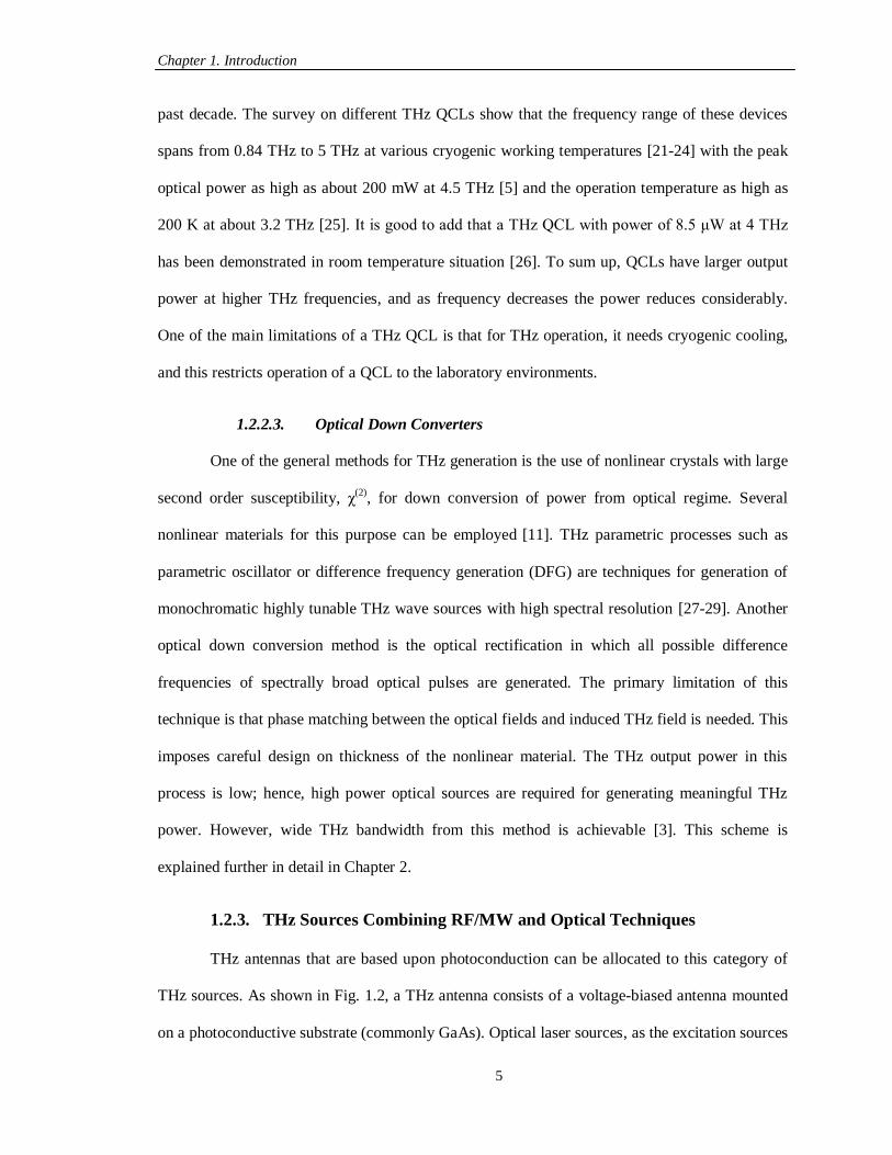
1.2.3. THz Sources Combining RF/MW and Optical Techniques
THz antennas that are based upon photoconduction can be allocated to this category of
THz sources. As shown in Fig. 1.2, a THz antenna consists of a voltage-biased antenna mounted
on a photoconductive substrate (commonly GaAs). Optical laser sources, as the excitation sources
Chapter 1. Introduction
6
of THz antennas, are used to produce THz waves by inducing rapid changes in the carrier density
of the photoconductive substrate. Depending on the type of optical excitation, there are basically
two alternatives for THz antennas based upon the photoconduction technique:
1) THz photoconductive antennas in pulsed systems
2) THz photomixer antennas in CW systems
Fig. 1.2 Schematic diagram of a THz antenna as an emitter for both pulsed and CW THz systems, showing
the optical laser illumination, photoconductive substrate, metallic antenna with a bias voltage, and the
antenna gap
Although it is possible to use the same antenna in both systems, different excitation
methods dictate different requirements for each antenna type and result in different THz waves
and applications. In THz pulsed systems, because of the external bias field, the optically induced
photo-carriers in the photoconductive gap give rise to rapid changes in the current density. These
currents induce a THz electromagnetic field in the connected antenna and as a consequence
ultrafast electrical pulses are produced and radiated into free space. In CW systems, the process is
the same; however, usually two monochromatic lasers with slightly different optical frequencies
(the difference is in THz) are used for THz emission from the antenna. This inherent excitation
difference in THz pulsed and CW systems, leads to the generation of ultra wideband and narrow
band THz waves respectively. In a CW system, the term of “photomixer” refers to the antenna
gap (which can have various designs) in analogy of “photoconductive gap” in a THz pulsed
Chapter 1. Introduction
7
system. The focus of this thesis will be on these types of sources. Detailed and comprehensive
study and investigation on THz antennas will be presented in next chapters.
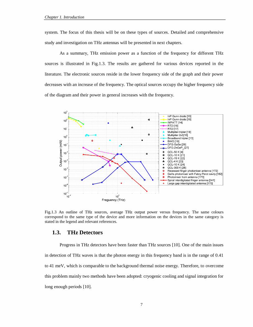
As a summary, THz emission power as a function of the frequency for different THz
sources is illustrated in Fig. 1.3. The results are gathered for various devices reported in the
literature. The electronic sources reside in the lower frequency side of the graph and their power
decreases with an increase of the frequency. The optical sources occupy the higher frequency side
of the diagram and their power in general increases with the frequency.
Fig.1.3 An outline of THz sources, average THz output power versus frequency. The same colours
correspond to the same type of the device and more information on the devices in the same category is
stated in the legend and relevant references.
1.3. THz Detectors
Progress in THz detectors have been faster than THz sources [10]. One of the main issues
in detection of THz waves is that the photon energy in this frequency band is in the range of 0.41
to 41 meV, which is comparable to the background thermal noise energy. Therefore, to overcome
this problem mainly two methods have been adopted: cryogenic cooling and signal integration for
long enough periods [10].
Chapter 1. Introduction
8
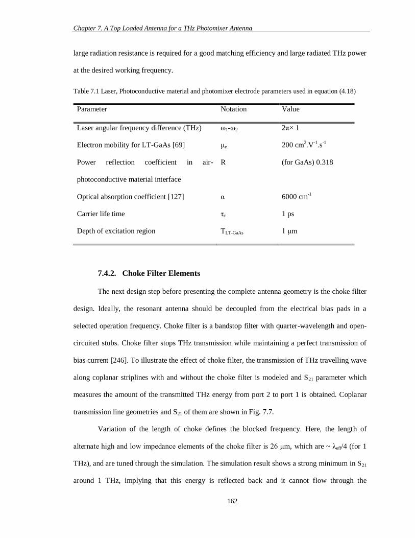
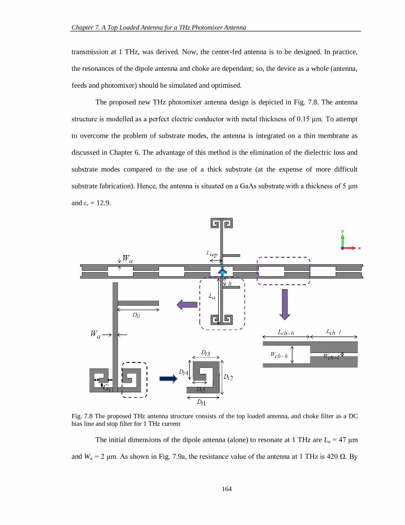
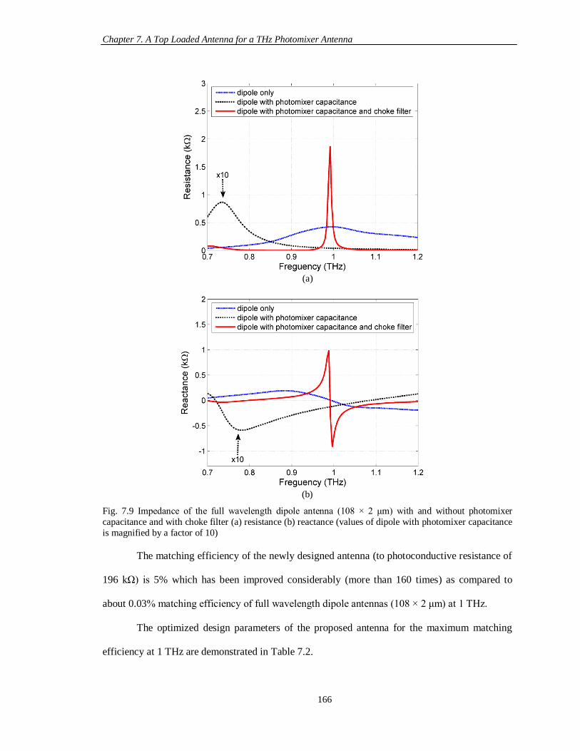
It is possible to categorize THz detection into coherent and incoherent techniques. The
main difference between them is that in coherent technique both the amplitude and phase of the
received signal are determined; but, in incoherent technique only the intensity of the signal is
measured.
Heterodyne detection is an important coherent technique in detecting weak and narrow
band signals. In this method a mixer, a non linear device, as a local oscillator is used for
frequency down conversion. The process of electronic heterodyne detection is demonstrated in
Fig. 1.4. The amplitude of the detected signal is proportional to the amplitude of the THz signal
[2]. There are various types of mixers in the THz range. A Schottky diode is a common and basic
mixer type for room temperature detectors where a modest sensitivity is required. However, for
high sensitivity applications, superconducting heterodyne detectors are employed which operate
in cryogenic temperatures. Superconductor–Insulator–Superconductor (SIS) tunnel junction
mixers and Hot Electron Bolometer (HEB) mixers are two examples of mixers in this category.
Fig. 1.4 Block diagram of a THz heterodyne detector
Electro-Optic (EO) and photoconduction samplings are also coherent methods. In the
former, the amplitude and phase of the THz signal are measured by using a nonlinear crystal. In
the latter type as shown in Fig. 1.5, the THz signal induces voltage across the antenna which leads
to generation of THz current due to the existence of free electron-hole pairs in the antenna gap.
The phase of the THz signal in these methods can be measured by varying the optical path length
of the optical probe pulse. Working principle of these methods is elaborated in Chapter 2.
Chapter 1. Introduction
9
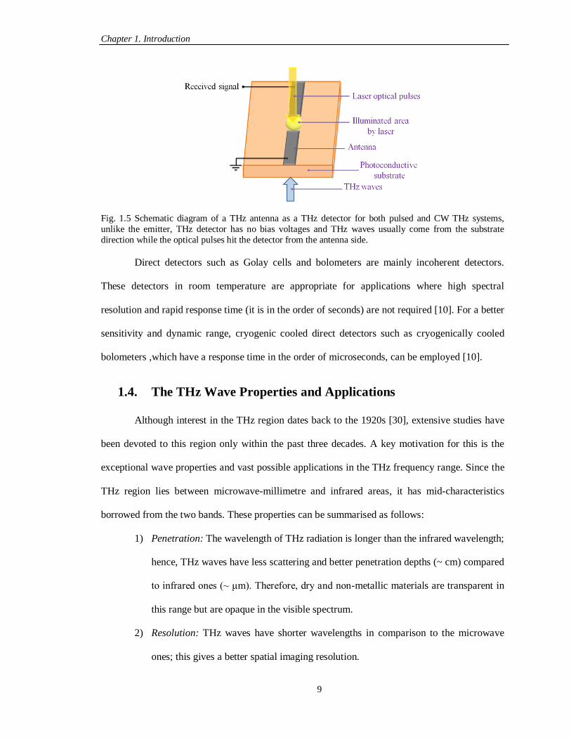
Fig. 1.5 Schematic diagram of a THz antenna as a THz detector for both pulsed and CW THz systems,
unlike the emitter, THz detector has no bias voltages and THz waves usually come from the substrate
direction while the optical pulses hit the detector from the antenna side.
Direct detectors such as Golay cells and bolometers are mainly incoherent detectors.
These detectors in room temperature are appropriate for applications where high spectral
resolution and rapid response time (it is in the order of seconds) are not required [10]. For a better
sensitivity and dynamic range, cryogenic cooled direct detectors such as cryogenically cooled
bolometers ,which have a response time in the order of microseconds, can be employed [10].
1.4. The THz Wave Properties and Applications
Although interest in the THz region dates back to the 1920s [30], extensive studies have
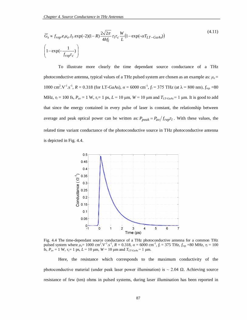
been devoted to this region only within the past three decades. A key motivation for this is the
exceptional wave properties and vast possible applications in the THz frequency range. Since the
THz region lies between microwave-millimetre and infrared areas, it has mid-characteristics
borrowed from the two bands. These properties can be summarised as follows:
1) Penetration: The wavelength of THz radiation is longer than the infrared wavelength;
hence, THz waves have less scattering and better penetration depths (~ cm) compared
to infrared ones (~ μm). Therefore, dry and non-metallic materials are transparent in
this range but are opaque in the visible spectrum.
2) Resolution: THz waves have shorter wavelengths in comparison to the microwave
ones; this gives a better spatial imaging resolution.
Chapter 1. Introduction
10
3) Safety: In contrast to X-rays, the photon energies in THz band are much lower.
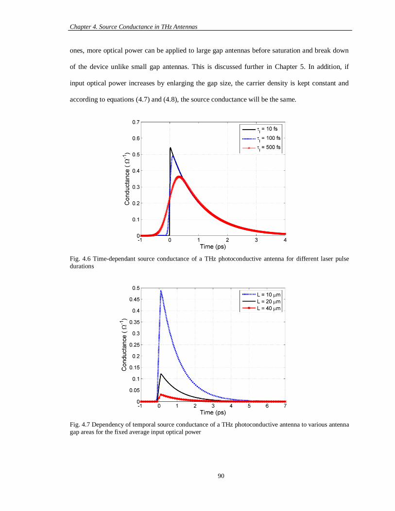
Therefore, THz radiation is non-ionising.
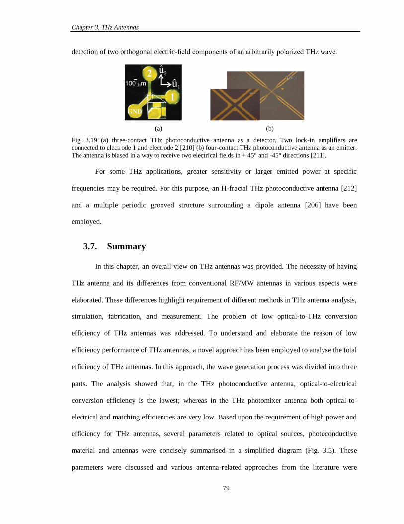
4) Spectral fingerprint: Inter- and intra-vibrational modes of many molecules lie in THz
range.
1.4.1. Atmospheric Characteristics of THz Waves
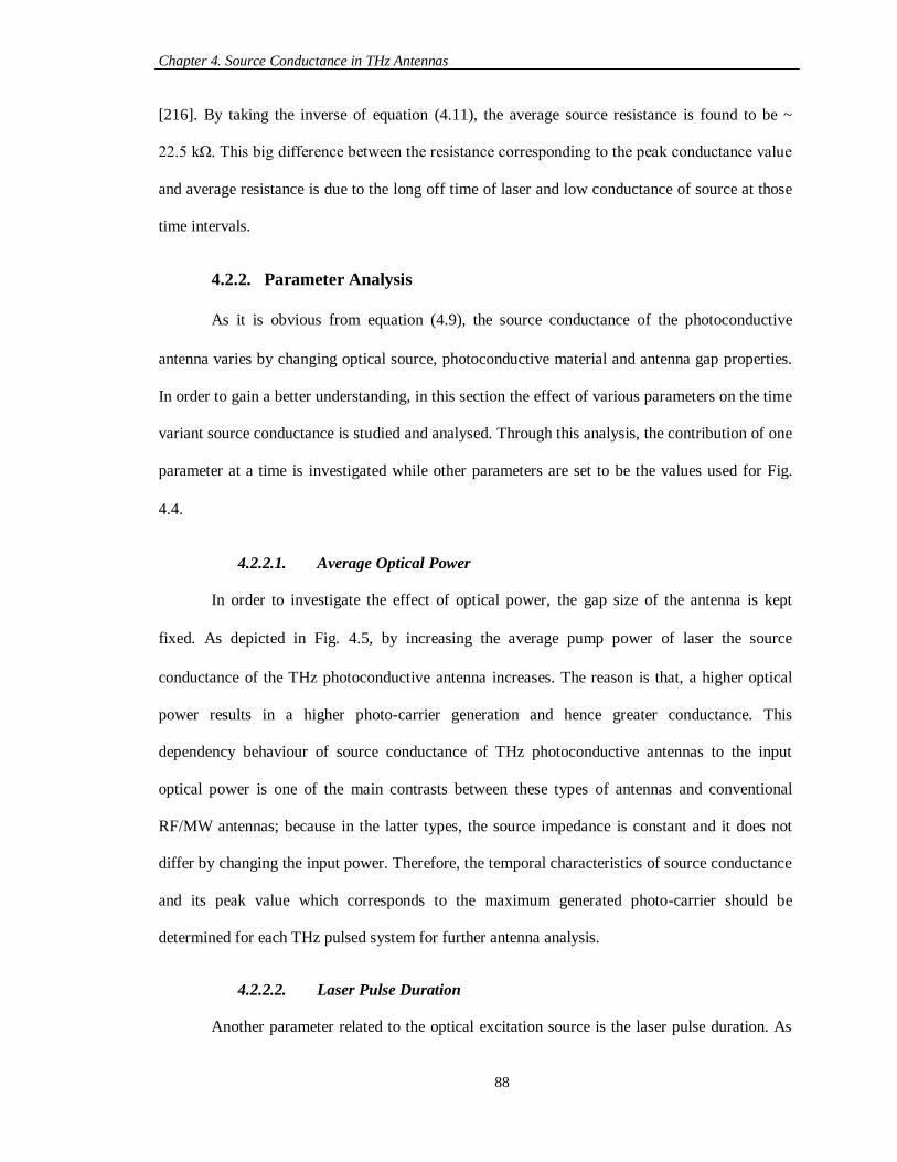
THz radiation has distinct atmospheric characteristics compared to the microwave and
infrared waves. THz waves have extremely high absorption in the atmospheric situation and the
moist environment. The atmospheric attenuation across the electromagnetic spectrum is depicted
in Fig. 1.6. It is obvious that signal degradation in this range- with the main peak attenuation
between 1 to 10 THz- is considerably more than microwave and infrared bands. THz signal
absorbs water significantly. Thus, for long range (> few hundred meters) applications the required
power for signal transmission is high and impractical [6]. However, application of THz waves in
the two following cases is different.
Fig. 1.6 Attenuation at sea level for different atmospheric situations, Rain = 4 mm/h, Fog = 100 m
visibility, STD = 7.5 g/m3 water vapour, and 2×STD = 15 g/m3 water vapour [31]1
1) In the space since the ambient is near-vacuum, signal absorption and attenuation due
1 This graph has originally been presented in [33]; however, due to better presentation quality, for
this thesis, it was taken from [31].
Chapter 1. Introduction
11
to water drops are not problems. Considering spectral signature of interstellar dust,
which is located in THz region, and aforementioned advantage of THz signals in
space, THz technology is a widely used technique in radio astronomy and space
science [10]. For instance, Herschel Space Observatory, the largest infrared space
telescope ever, was launched in 2009 in the THz region by the European Space
Agency [32].
2) For short range applications (< 100 m [6]), atmospheric attenuation is not a
significant issue. Hence, THz technology is a very versatile tool for fundamental
investigations in various disciplines such as physics and chemistry.
It is good to add that despite adverse effect of water vapour lines on THz signals, these
lines are narrow enough, and their positions have been known. Thus, this allows
removal/recognition of their effect in THz applications such as spectroscopy [33].
1.4.2. Applications of THz Radiation
Based upon THz wave properties, THz radiation can be applied in many possible
applications including imaging, spectroscopy and wireless communication [11, 34, 35]. Although
THz applications have been widely investigated, only in the recent decade several commercial
THz imaging and spectroscopy systems have entered the market by companies such as TeraView
Ltd [36], Picometrix [37] and Toptica [38]. The first ever THz camera that can see and record in
real-time at room temperature was introduced in early 2011 by Traycer [39]. Since the focus of
this thesis is on THz antennas, THz applications related to optoelectronic (both pulsed and CW)
systems are only briefly discussed in this section.
1.4.2.1. THz Pulsed System Applications
Since the work of pioneers in THz pulsed imaging [40] and THz CW imaging [41],
applications based on THz imaging have been the focus of many research areas [34]. Indeed,
medical imaging is one of the main subcategories in this field. THz waves can penetrate up to a
Chapter 1. Introduction
12
few hundred micrometers (μm) in human tissues; therefore, it is a possible method for body
surface diagnosis such as skin, breast and mouth cancer detection [36, 42, 43] and dental imaging
[44]. Some of the benefits of this method can be named as, early detection of cancerous tissues
and tooth decay or minimisation of the damage to the surrounding healthy skin in biopsy [36].
THz medical imaging has two major drawbacks; the equipment is expensive and data acquisition
time is long. The latter disadvantage has been addressed by employing arrays of antennas and
micro lenses [34].
THz pulsed spectroscopy has been another fascinating application for commercialising
THz technology in diverse areas [10] since the first introduction of this method in [45]. Now THz
spectroscopy is a very powerful technique to characterise material properties and understand their
signature, which lies in the THz band (many molecules have rotational and vibrational transition
lines in this range of frequency). One type of interesting THz spectroscopy applications is in
biochemical science such as analysis of DNA signatures and protein structures [46].
Also, THz radiation is a suitable technique to investigate material integrity and inspect
multi-layered materials such as wood, composites, and clothes which are transparent in THz
frequencies. THz pulsed imaging and spectroscopy has been adopted for non-destructive testing;
for example, on imaging antiquities [47, 48] to reveal the thickness of the different layers of the
art work and to show types of their materials [49]. This technique can be used for in-line control
of polymeric compounding processes as well [50].
Furthermore, THz pulsed imaging and spectroscopy are two strong quantitative and
qualitative non-invasive methods for examining pharmaceutical solid dosage forms [51, 52].
THz systems have the potential market for security applications [34] because of the
possibility of using these systems in personnel screening [36], solid explosive material detection
[53, 54], and mail screening [55]. However, metals are not transparent to THz signals; therefore,
they are not suitable for imaging inside the metallic suitcases. This method can be treated as a
complementary scheme for the well-established monitoring techniques like X-ray [34].
Chapter 1. Introduction
13
Although high water absorption is one of the drawbacks of the THz technology, it can be
manipulated positively to distinguish the hydrated substances from dried ones. For instance, in
the paper industry, THz spectroscopy has been used for monitoring the thickness and moisture
content of papers by manufacturers [56, 57].
Last but not least, THz pulsed imaging is a very convenient method to take 3D images
from the inside of an integrated circuit device as compared to 2D images provided by the X-ray
method [36].
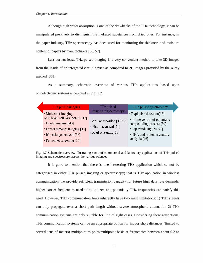
As a summary, schematic overview of various THz applications based upon
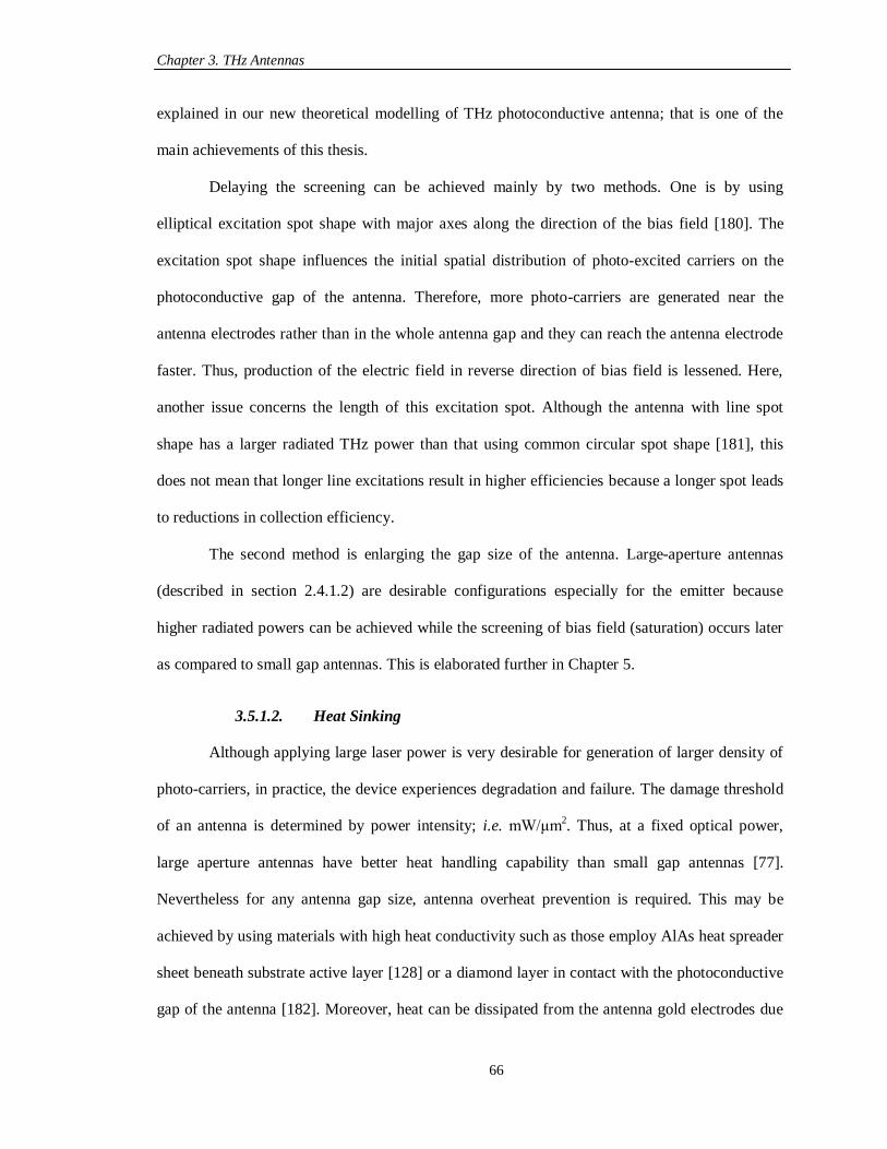
optoelectronic systems is depicted in Fig. 1.7.
Fig. 1.7 Schematic overview illustrating some of commercial and laboratory applications of THz pulsed
imaging and spectroscopy across the various sciences
It is good to mention that there is one interesting THz application which cannot be
categorised in either THz pulsed imaging or spectroscopy; that is THz application in wireless
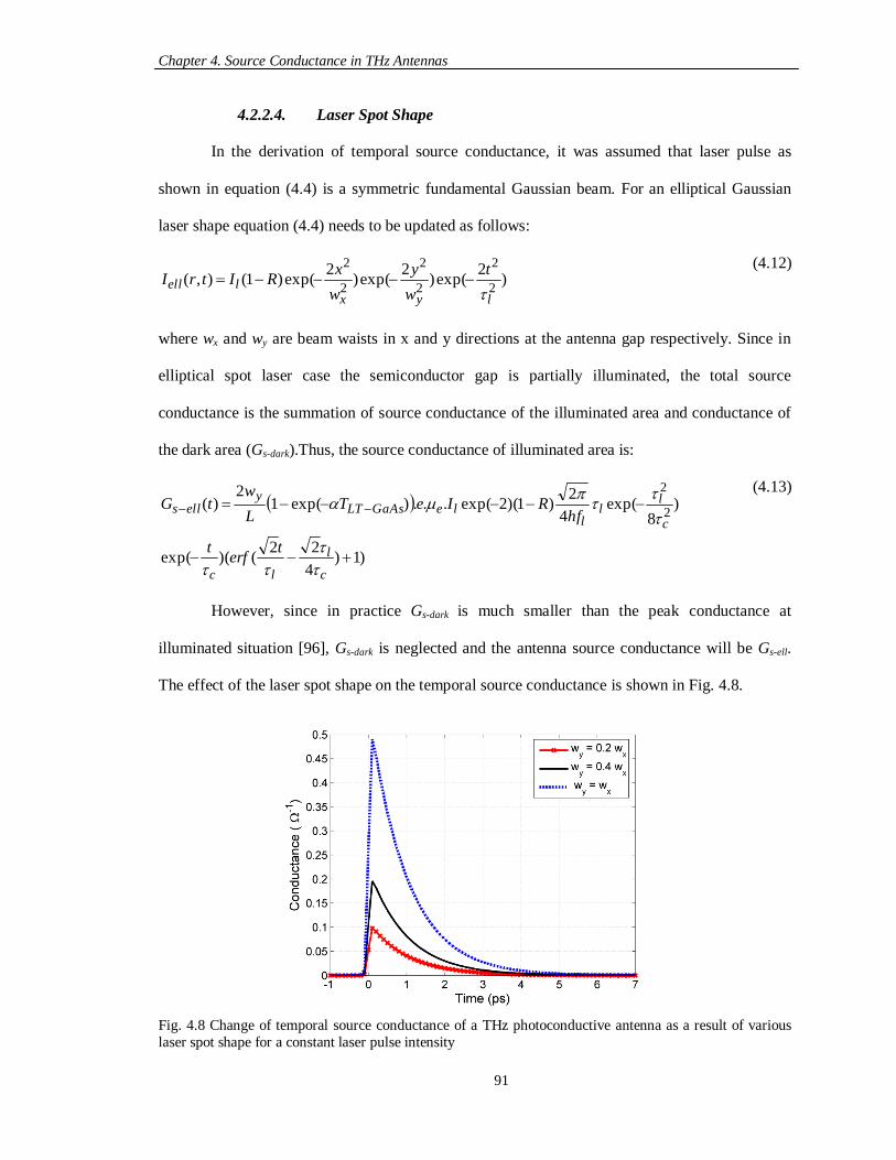
communication. To provide sufficient transmission capacity for future high data rate demands,
higher carrier frequencies need to be utilized and potentially THz frequencies can satisfy this
need. However, THz communication links inherently have two main limitations: 1) THz signals
can only propagate over a short path length without severe atmospheric attenuation 2) THz
communication systems are only suitable for line of sight cases. Considering these restrictions,
THz communication systems can be an appropriate option for indoor short distances (limited to
several tens of meters) multipoint to point/multipoint basis at frequencies between about 0.2 to
Chapter 1. Introduction
14
0.3 THz [58]. From another point of view, these restrictions are beneficial for secure THz
communication. Since the beam can be highly directional and it attenuates severely over the
distance, unwanted signal detection is very difficult. Some THz data communications for short
ranges (< 1m) based upon THz time domain systems have been tested at 0.3 THz in recent years
[59]. In [60] external semiconductor THz modulator is used and in [61] audio signals through the
voltage of the transmitter THz antenna modulates the THz frequency. Block diagrams of these
two approaches are demonstrated in Fig. 1.8.
(a)
(b)
Fig. 1.8 Schematic diagram of THz communication links for (a) system of [60] with external modulator (b) system of [61] where voltage modulation of the THz antenna is used.
1.4.2.2. THz CW applications
Although THz pulsed imaging and spectroscopy can provide data on broadband
frequency ranges, for some applications, such as gas-phase spectroscopy, high frequency
dielectric measurements of electronic, metamaterials and nano-materials, and analyses of
signatures in microliter DNA, narrowband high resolution systems are required [36, 62-64]. THz
Chapter 1. Introduction
15
CW imaging and spectroscopy systems can provide such an opportunity [65, 66]. It is good to add
that for some applications like imaging of aircraft glass-fibre composites or determining the
thickness of a sample, both pulsed and CW imaging methods can be used [59, 67].
1.5. Research Motivations and Objectives
A major limitation of the fast growing THz technology is the development of high output
power and efficient sources – this is the primary motivation for this research.
In spite of explained fascinating and unique properties, THz technology has been largely
avoided by the late of the twentieth century due to the lack of robust, coherent, efficient and cost
effective THz sources and detectors. However, the advent of femtosecond lasers in the 1980s and
later photoconductive antennas by Austin in 1984 [68] revolutionised accessibility to THz gap.
Since then and over the last three decades, THz technology has witnessed unprecedented
progresses due to interests in exciting THz applications in different fields as discussed previously.
Some commercial THz imaging and spectroscopy systems have been introduced to the market;
nevertheless, there are various issues, such as the low output power and working temperature of
THz sources, which need to be addressed to ripen this technology like radio and optical
technologies.
THz antennas based upon the photoconduction method are one of the key and common
components in many THz systems. The popularity of these THz antennas is because of the
several advantages that they offer as compared to the other THz sources discussed earlier. For
instance, they work in the room-temperature environment, they are compact, and they can operate
both in the emission and detection sides. Although these types of components have been widely
employed in established THz systems, the radiated power from them is very low (about few
microwatts) and they are inefficient [69]. For this purpose, it is crucial to distinguish the effect of
various parameters of optical sources, photoconductive materials and antennas on the
performance of the THz antennas. Thus, having a model which links these parameters can be very
Chapter 1. Introduction
16
useful for both, designing a THz antenna and tuning a THz system to achieve the maximised
power conversion efficiency and THz radiated power. Therefore, as a fundamental research work
on the THz photoconductive antennas, an analytical model is developed in this study considering
the interaction between laser beams, photoconductive materials and antennas in a typical THz
scheme.
Using a package of commercial simulation tool is an essential part of RF antenna
analysis. However, the major difference in analysing THz antennas as compared to RF antennas
is the optoelectronic characteristics of THz antennas which are the result of the optical excitation
and photoconductive material response. Some commercial semiconductor solvers such as TCAD
Sentaurus [70] perform advanced simulations on characterising semiconductor devices
considering their complex physical phenomena; and various information for instance on electric
field distribution and charge concentration can be provided by them. However, for THz antenna
analysis the THz current source is the main input that needs to be fed to full-wavelength
simulation tools. Considering the required information, although the combination of
semiconductor solvers with full-wave electromagnetic solvers can provide possibility of
simulation of THz antennas, this method can be an expensive process. Thus, a new simulation
and analysis procedure is developed that eliminates the requirement for two commercial tools.
The THz current source can be analysed through the proposed analytical method and then antenna
performance can be examined with a full-wave electromagnetic solver.
Furthermore, considering the difference in optical excitation sources of THz
photoconductive antennas and THz photomixer antennas, different analysis method and antenna
design considerations is required. Hence, the response of photoconductive material which acts as
the source resistance for the antenna is examined and compared for both methods.
A THz photomixer antenna is usually integrated with electrodes, an antenna and a lens.
Electrodes are main components which are responsible for generation of THz current.
Geometrical modification and optimisation of electrodes can lead to generation of more THz
Chapter 1. Introduction
17
current which couples to the antenna. Configuration of electrodes accompanied by
photoconductive material characteristics also affects the source resistance of the antenna.
Designing an antenna which has good impedance matching to the source resistance is very
important because it results in an improved radiated THz power. In addition, coupling of the
created THz field to air is crucial to have a directional pattern. Thus, in order to improve the
radiated THz power, modifications in these components are required. By considering the role of
each part, in this research an improved THz photomixer antenna is proposed and studied. Then,
the performance of the new photomixer design (used with a common bowtie antenna) is
characterised and evaluated.
As a summary, the main objectives of this research are as follows:
To improve the radiated THz power and efficiency of photoconductive antennas
To develop a new model which will encapsulate various THz antenna parameters and
can be used for antenna performance analyses
To develop a simulation method for THz photoconductive analysis
To develop and characterise an antenna solution for THz CW systems
1.6. Thesis Overview
The thesis is organized as follows. Chapter 2 reviews THz time domain generation and
detection systems based upon the antennas and EO crystals. It provides a comparison on
performance of THz systems based upon THz photoconductive antennas and EO crystals with the
aim of choosing the suitable pairs for THz applications. Also, the differences of THz pulsed
systems and THz CW systems are addressed from the excitation source, system arrangement and
system characteristics points of views. This is required to provide a big picture on the THz
antenna position and its importance in a THz system.
To narrow down the scope of the research to THz antennas, Chapter 3 starts with
providing comparisons of THz antennas with conventional RF/MW antennas from various
Chapter 1. Introduction
18
aspects. This highlights necessity of the new look and approach on analysis of THz antennas as
compared to RF/MW antennas, and it builds the foundation for the contributions of this thesis. In
the second part of this chapter, the problems and reasons for THz antennas having low efficiency
are elaborated, and some of the previous work on the performance improvement of THz antennas
is reviewed.
Based upon the antenna feeding method in THz antennas, a new time-varying source
conductance for THz photoconductive antennas is derived in Chapter 4. Effects of various
parameters on the temporal behaviour of source conductance are discussed. Furthermore, source
conductance (or 1/resistance) of THz photoconductive antennas and THz photomixer antennas
are compared to show the difference of this antenna parameter based upon the excitation of the
antenna. This is important for antenna matching efficiency evaluations.
Chapter 5 introduces a novel theoretical model of a photoconductive antenna in a THz
pulsed system. This model uses physical concepts of THz wave generation and incorporates these
principles to develop a new lumped-element network. Radiated power and optical-to-THz power
conversion efficiency of a THz antenna based upon this model are studied, and the analytical
results are obtained and compared with measured results from the literature.
Other two differences of THz antennas with RF/MW antennas are in the electrical
thickness of the substrate and computer aided design procedures. These two are addressed in
Chapter 6. First, effect of varying substrate thickness on performance of a THz antenna is
reviewed and compared with the simulation result. In the second part, a new simulation method
for characterising a THz photoconductive antenna is presented. Effect of several parameters of
the system on the spectral THz emission is examined, and the procedure is validated by
comparing the achieved results from this technique with the published measurement results in the
literature.
A new photomixer antenna for THz CW systems is proposed in Chapter 7. A novel
concept for enhancing the generated THz photocurrent in the photomixer is elaborated. Then, an
Chapter 1. Introduction
19
antenna for enhancing the matching efficiency and improving radiation directivity is introduced.
The antenna operation principle, design procedure, simulated and measurement results are
systematically described in this chapter.
Finally, Chapter 8 draws the conclusion of the work. The main objectives are reviewed,
and the achievements are highlighted. Furthermore, the challenges and suggestions worthwhile to
investigate as future research topics are presented.
Chapter 2. THz Generation and Detection Systems
Based upon the Antenna
2.1. Introduction
Various THz sources and detectors and also fascinating applications of THz technology
were described in the previous chapter. Since the focus of this thesis is on THz antennas, in order
to go one step forward on analysing the performance of this type of devices, it is important to
consider the operation of the entire THz system of which the antenna is a crucial part of it.
Therefore, the main objective of the current chapter is to study and investigate how THz
generation and detection systems perform based upon the antennas employed.
In many established THz pulsed and CW systems, femtosecond laser pulses and CW
laser sources are respectively used to excite optoelectronic sources as a start point of the system.
Therefore, the characteristics of these laser sources are explained as a necessary background for
the next chapters. The common optoelectronic emissive and detective components are THz
antennas and EO crystals. In THz pulsed systems, different combinations of these components
can be used as the emitter and detector. For the THz system analysis, in this chapter, the working
principle and effective design parameters of EO crystals and THz photoconductive antennas are
firstly discussed. After that, two different systems (one is the photoconductive antenna and the
other is EO crystal as the emitter whilst in both cases EO crystal is the detector) are characterised
in the THz pulsed system and examined from the signal-to-noise ratio (SNR) and bandwidth
Chapter 2. THz Generation and Detection Systems Based upon the Antenna
21
points of view. Furthermore, the merits of four ultra-wideband THz generation and detection
systems using ultra-short laser pulses (< 20 fs) are reviewed. The goal of comparing these
systems based upon EO crystals and/or photoconductive antennas is to aid the selection of the
appropriate emitter-detector combination when setting up a THz coherent generation and
detection system. Finally, in order to have a comprehensive summary on THz systems based upon
THz antennas, other THz systems, namely THz CW systems and THz quasi time domain
systems, are also briefly reviewed.
2.2. The Laser Pulses
The starting point of a THz system is a laser source. In a THz pulsed system, the time
dependent electric field from a typical femtosecond laser source such as Ti: sapphire is depicted
in Fig. 2.1a. The optical power, wavelength (1/frequency), pulse duration (defined by taking the
full width at half maximum of the laser power), τl, and the pulse repetition time, trep, are the
features that describe the characteristics of the radiated optical pulses.
The common photoconductive material, which is LT-GaAs, has the energy gap of 1.43
eV; therefore, the optical pulses should have larger photon energy to excite a single photon in LT-
GaAs. This implies that the wavelength of laser pulses should be smaller than 867 nm. The pulse
duration of femtosecond lasers is typically smaller than 200 fs and it even approaches 10 fs [71,
72]. The laser repetition rate (1/trep) is typically smaller than 100 MHz, and it indicates the
amount of delivered energy per pulse according to the average optical power of laser (optical
energy = average optical power /laser repetition rate). Fig. 2.1b shows the spectrum of a
femtosecond laser pulse which it has a broad spectral distribution.
In a CW system, the electric fields of two above-bandgap monochromatic CW lasers
(such as laser diodes) mix. Their angular frequencies, ω1 and ω2, are slightly different; as a result,
the beating waveform at the photoconductive surface with angular frequencies of ω2-ω1 and
ω2+ω1 are produced [73]. In Fig. 2.2a the temporal resulting optical electric field is schematically
Chapter 2. THz Generation and Detection Systems Based upon the Antenna
22
shown and Fig. 2.2b illustrates the corresponding frequency spectrum of two single mode laser
waves and the eventual optical waves. The term of ω2-ω1 is located at THz frequencies and the
photoconductive substrate only able to respond to this frequency, which is the envelope of the
produced waveform shown in Fig. 2.2a.
(a) (b)
Fig. 2.1 Schematic diagram of (a) temporal electric field of optical laser pulses at the photoconductive substrate for a pulsed system (b) corresponding spectral distribution of electric field of an ultra-short pulse
(a)
(b)
Fig. 2.2 Schematic diagram of (a) temporal (b) spectral electric field of optical laser pulses at the
photoconductive substrate for a CW system
2.3. The EO Crystal
An EO crystal can be used as an emitter and a detector in a THz pulsed time domain
Chapter 2. THz Generation and Detection Systems Based upon the Antenna
23
system. ZnTe is the most commonly used EO crystal in THz pulsed systems with large second
order nonlinear optical susceptibility of χ(2)
. When EO crystals are employed as emitters, the
radiation occurs due to response of electrons in the matter and their acceleration because of
external electromagnetic waves. The energy of the THz radiation is extracted directly from the
laser pulses and it is based on optical rectification process. Optical rectification is the generation
of all possible difference-frequency components that exist in the broad frequency spectrum of
ultra-short optical pulses.
There are some features in EO crystals that affect the generated THz waves. These
factors can be summarised as follows:
χ² affects the nonlinear polarisation and hence, it affects differently the radiated THz
field in each tensor direction of nonlinear crystal. For instance, in ZnTe when optical
polarisation lies in (110) plane the THz intensity can be maximised [2].
In an ideal case in an EO crystal, it is desirable to have an equal optical refractive
index and THz refractive index at all frequencies. This is required to satisfy the
velocity matching condition between the optical and THz waves. Since the radiated
THz electric field is proportional to the crystal thickness, THz wave is amplified
while propagating through the crystal. However, in reality EO crystals have
dispersive behaviour and this leads to destructive interference between THz
waveforms. Thus, for broadband THz waves, the requirement of similarity in optical
group velocity and the phase velocity of the central frequency of the THz spectrum
can be met only at certain frequencies [2]. In order to alleviate this velocity mismatch
the crystal should be kept thin. Therefore, there is a trade-off between the thick
crystal for larger amplitude of THz field and thin crystal for velocity matching
condition and avoiding destructive interference.
When an EO crystal is used as a detector, the incident THz field induces birefringence in
the crystal. In other words, the crystal responds to the polarisation and the direction of the THz
Chapter 2. THz Generation and Detection Systems Based upon the Antenna
24
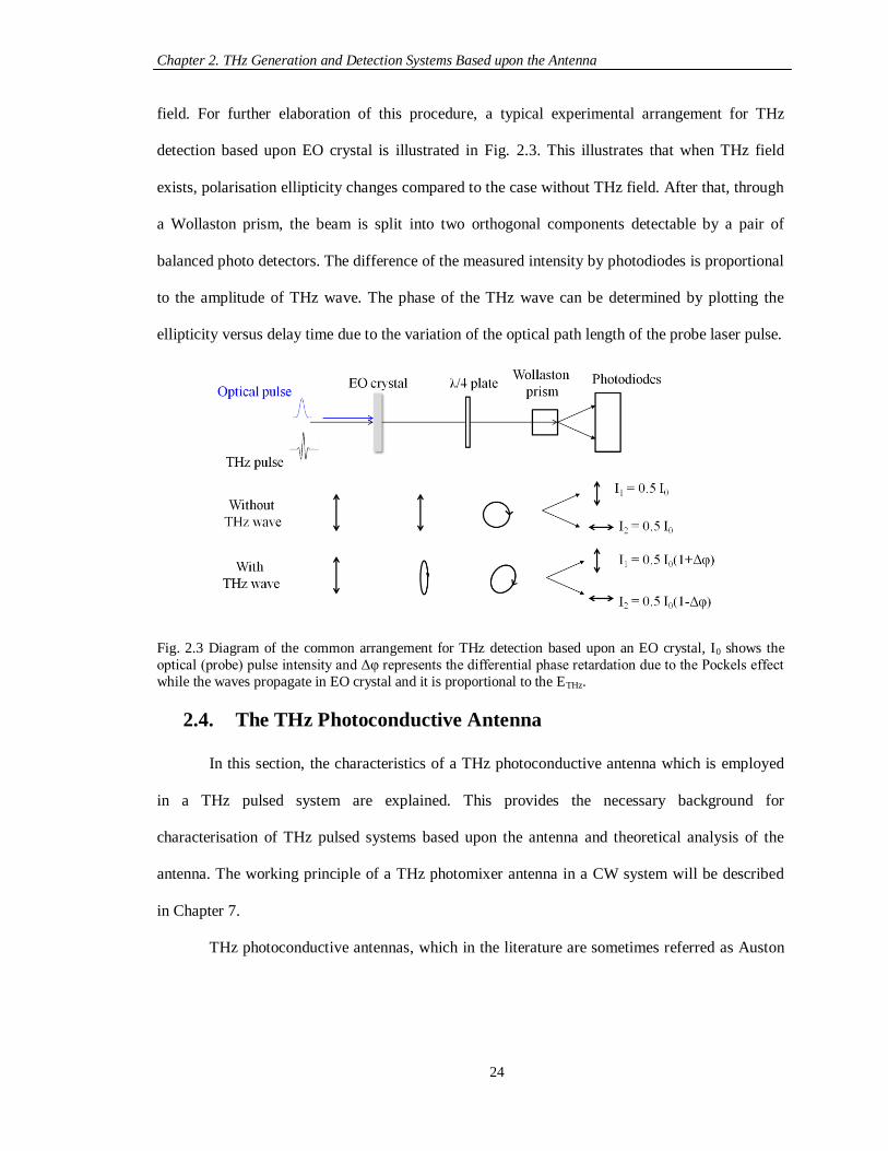
field. For further elaboration of this procedure, a typical experimental arrangement for THz
detection based upon EO crystal is illustrated in Fig. 2.3. This illustrates that when THz field
exists, polarisation ellipticity changes compared to the case without THz field. After that, through
a Wollaston prism, the beam is split into two orthogonal components detectable by a pair of
balanced photo detectors. The difference of the measured intensity by photodiodes is proportional
to the amplitude of THz wave. The phase of the THz wave can be determined by plotting the
ellipticity versus delay time due to the variation of the optical path length of the probe laser pulse.
Fig. 2.3 Diagram of the common arrangement for THz detection based upon an EO crystal, I0 shows the
optical (probe) pulse intensity and Δφ represents the differential phase retardation due to the Pockels effect
while the waves propagate in EO crystal and it is proportional to the ETHz.
2.4. The THz Photoconductive Antenna
In this section, the characteristics of a THz photoconductive antenna which is employed
in a THz pulsed system are explained. This provides the necessary background for
characterisation of THz pulsed systems based upon the antenna and theoretical analysis of the
antenna. The working principle of a THz photomixer antenna in a CW system will be described
in Chapter 7.
THz photoconductive antennas, which in the literature are sometimes referred as Auston
Chapter 2. THz Generation and Detection Systems Based upon the Antenna
25
switches [74]1, consist of two metal (usually gold) electrodes on a photoconductive substrate.
These electrodes act mainly as a means for biasing the device (when used as an emitter)
and also as an antenna. The distance between the electrodes is referred as the photoconductive
gap and it is the main part where the laser pulses illuminate and electron-hole pairs are produced.
From photoconductive gap size point of view, THz photoconductive antennas can be categorised
into three types; small gap antennas with gap size of about 5 to 50 μm, large-aperture antennas
where the gap dimension is much greater than the centre wavelength of the emitted THz radiation
(gap sizes are usually larger than few hundred micrometers) [75], and semi-large gap antennas
which the gap size is between the two previous types [76]. Two main advantages of semi-large
and large-aperture antennas are ease of fabrication, and better heating handling capability due to
larger deposited electrode areas on the substrate [77]. On the other hand, with small gap antennas,
larger spectral ranges can be achieved as compared to large-aperture antennas [76, 78]. Electrodes
of a THz antenna are more influential on the THz power and bandwidth of a small gap antennas
rather than large-aperture antennas [76]. More detailed performance comparison of small gap and
large-aperture antennas are provided in next chapters.
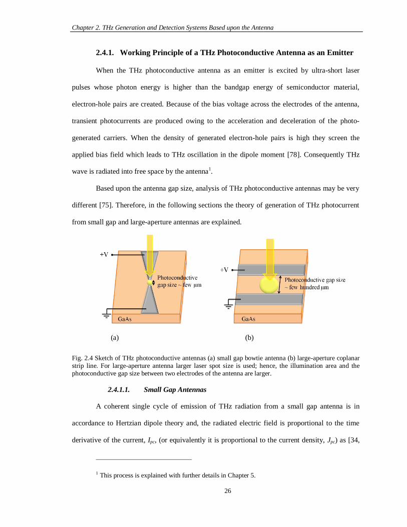
An antenna electrode can have various shapes and some typical antenna geometries are
illustrated in Fig. 2.4. Bowtie antennas are one of the favourable antenna types in THz pulsed
systems due to their frequency independent characteristics. Moreover, the sharp ends of the
antenna lead to high electric fields; hence, THz radiation from the device is enhanced [79]. A
large gap coplanar strip line is favoured because it does not need necessarily micro-fabrication
techniques like small gap antennas, and also it is not as sensitive as small gap antennas to laser
focus alignment.
1 The main difference of original Auston switch with a photoconductive antenna is that in an
Auston switch two lasers with different wavelengths have been employed for turning the switch on and off;
however, in a THz photoconductive antenna only one wavelength laser pulses are used.
Chapter 2. THz Generation and Detection Systems Based upon the Antenna
26
2.4.1. Working Principle of a THz Photoconductive Antenna as an Emitter
When the THz photoconductive antenna as an emitter is excited by ultra-short laser
pulses whose photon energy is higher than the bandgap energy of semiconductor material,
electron-hole pairs are created. Because of the bias voltage across the electrodes of the antenna,
transient photocurrents are produced owing to the acceleration and deceleration of the photo-
generated carriers. When the density of generated electron-hole pairs is high they screen the
applied bias field which leads to THz oscillation in the dipole moment [78]. Consequently THz
wave is radiated into free space by the antenna1.
Based upon the antenna gap size, analysis of THz photoconductive antennas may be very
different [75]. Therefore, in the following sections the theory of generation of THz photocurrent
from small gap and large-aperture antennas are explained.
(a) (b)
Fig. 2.4 Sketch of THz photoconductive antennas (a) small gap bowtie antenna (b) large-aperture coplanar
strip line. For large-aperture antenna larger laser spot size is used; hence, the illumination area and the
photoconductive gap size between two electrodes of the antenna are larger.
2.4.1.1. Small Gap Antennas
A coherent single cycle of emission of THz radiation from a small gap antenna is in
accordance to Hertzian dipole theory and, the radiated electric field is proportional to the time
derivative of the current, Ipc, (or equivalently it is proportional to the current density, Jpc) as [34,
1 This process is explained with further details in Chapter 5.
Chapter 2. THz Generation and Detection Systems Based upon the Antenna
27
80]1:
t
tJ
t
tItE
pcpcTHz
)()()(
( 2.1)
The photocurrent itself is generated due to the movement of electrons from the valence
band to the conduction band under laser illumination. Assuming the electron (free carrier) density
in the conduction band is n(t) and the velocity of carriers is v(t), the current density, Jpc (t), is
given by [81]:
)()()( tvtnetJ pc
( 2.2)
where e is the electron charge. The same current relation, but with a positive sign, holds for the
hole. However, since the effective mass of a hole is much larger than that of the electron its
contribution to THz current and radiation is much smaller [82]; hence it can be neglected.
For explaining main features of this photocurrent density and carrier dynamics, a simple
one-dimensional Drude-Lorentz model has been developed by Jepsen et al. [78]. This model
consists of three interlinked differential equations describing the relation of free carrier density,
the velocity of carriers, and the polarisation caused by separated carriers under the bias field, Psc.
These equations are as follows:
)()()(
tGtn
dt
tdn
c
( 2.3)
locals
Em
etv
dt
tdv*
)()(
( 2.4)
sc
biaslocalP
EE
( 2.5)
)(tJP
dt
dPpc
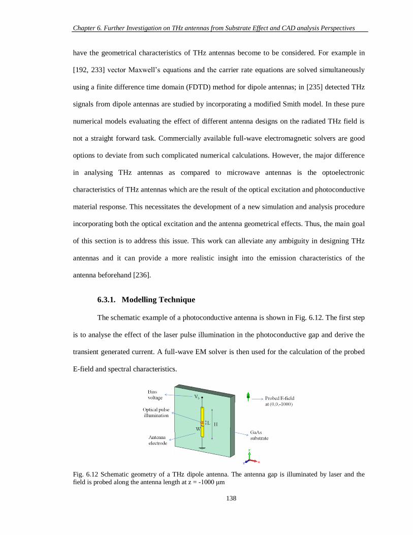
r
scsc
( 2.6)
where τc is the carrier trapping time (or carrier lifetime) and defined as the average time span that
1 The detailed derivation of this equation through vector potential relations and the time-varying
behaviour of the Hertzian dipole is presented in Appendix A.
Chapter 2. THz Generation and Detection Systems Based upon the Antenna
28
excess free electrons survive before falling into an energy level caused by the presence of a defect
(“trap”), τs is the momentum relaxation time (or carrier scattering time) defined as the average
time between two collisions of each electron in the conduction band and it is in the order of the
tenth of ps [81], τr is the carrier recombination lifetime which is very long and defined as the
average time that electrons move from the “trap” into an empty valence band state [83], G(t) is
the generation rate of carriers by laser pulses, m* is the effective mass, Elocal is the electric field in
the photoconductive gap, Ebias is the applied bias to antenna electrodes, and ζ is the geometrical
factor [78]. Through numerical calculations of equations ( 2.3)-( 2.6), it is possible to find Jpc(t)
and ETHz(t). Therefore, considering equations ( 2.1) and ( 2.2), the radiated THz field can be related
to carrier dynamics and calculated as:
dt
tdvtnetv
dt
tdne
t
tJtE
pcTHz
)()()(
)()()(
( 2.7)
This demonstrates two phenomena of 1) ultrafast variation in carrier density and 2)
acceleration of photo-carriers, which together result in THz radiation. Applying large optical
power and large bias field are two main methods that lead to enhancement of aforementioned
factors respectively and as a result, increased THz radiation. However, there are some limitations
on increasing these parameters. In Chapter 3, the methods that can improve THz power are
comprehensively reviewed.
2.4.1.2. Large-Aperture Antennas
Emission of THz radiation from the large-aperture antenna is in accordance with the
dipole antenna theory. Under laser illumination, the generated photocurrent can be assumed as
surface current confined to a thin layer in the photoconductive gap [2, 75, 84]. Therefore, the on–
axis radiated THz field in the temporal format can be written as [84]:
dt
tJd
z
S
r
dS
t
tJtrE ss
THz)(
4
)(
4),(
( 2.8)
where, μ is the permeability, S is the photo-excited area in the antenna gap, r is the observation
Chapter 2. THz Generation and Detection Systems Based upon the Antenna
29
distance, z is on-axis distance from the antenna gap, and )(tJs
is the surface current density.
According to the detailed explanations in Appendix A, the radiated THz field can be
obtained as:
bias
r
e
e
bias
r
s
s
THz E
tne
dt
tdne
z
SE
t
dt
td
z
StzE
2
0
2
0 11
)(
)(
4
11
)(
)(
4),(
( 2.9)
where μe is the mobility.
By comparing equations ( 2.7) for small gap and ( 2.9) for large-aperture antennas, it can
be interpreted that different antenna gap sizes impose different analysis criteria and different
equations for the radiated THz field. The focus of this thesis is on small gap antennas.
2.4.2. Working Principle of a THz Photoconductive Antenna as a Detector
Essentially THz detection by photoconductive antennas is the reverse of the generation
mechanism. In detection, no bias voltage is applied across the electrodes, and the incident THz
radiation induces voltage across the antenna which accelerates photo-carriers generated by the
gating laser pulse (which is the portion of the optical source). By a variable time delay, the arrival
time of the gating pulse can be adjusted; thus, the temporal behaviour of the photocurrent due to
THz radiation can be measured by a current meter (lock-in amplifier). The detected photocurrent
at a time delay of t can be explained based upon Ohm’s law as shown in equation ( 2.10).
tdttnetEttEtJ reTHzTHz )()()()()( detdet
( 2.10)
where σdet(t) represents the time-varying conductivity of the detector, ETHz(t) is the received THz
signal on the detector, and nr(t) is the generated photo-carrier density by the gating pulse [80].
Based upon the behaviour of photo-carrier density two extreme situations can be
assumed. If )()( ttnr (for photoconductive materials with ultra-short carrier lifetime) then
detected current from equation ( 2.10) will be proportion to the original income THz signal; i.e.
Chapter 2. THz Generation and Detection Systems Based upon the Antenna
30
)()(det fEfJ THz . On the other end, if it is presumed that nr(t) has a behaviour like a step
function (for materials with extremely long carrier lifetime like SI-GaAs); then
ffEfJ THz )()(det . This demonstrates that characteristics of the photo-carrier density in the
detector antenna and its decay behaviour affect the bandwidth of the detected signal. The in-
between case is the realistic situation where distortion effect of the detector on the incident THz
field is considered by convolving the detector response with THz field (in the time domain) [82].
Thus, the detected photocurrent for the in-between situation can be explained considering the
spectral behaviour of laser pulses, Il(f), and the frequency response of excited photo-carriers in the
photoconductive antenna, B(f), as equation ( 2.11) [34, 85].
)()()()(det tEfBfIfJ THzl ( 2.11)
The response time of the detector determines the amount of detected signal at high
frequencies(B(f)). This is governed by carrier lifetime of photoconductive material and RC time
constant related to the device capacitance [86]. In other words, a THz photoconductive antenna
on the detector side acts as a low pass filter [82].
2.5. The THz Pulsed Systems
Although various types of THz sources and detectors exist (as explained in Chapter 1),
generally established THz pulsed systems are combinations of a photoconductive THz antenna
and an EO crystal. Based upon the type of the application (spectroscopy and imaging), a THz
systems is named as THz Time Domain Spectroscopy (THz-TDS) and THz Time Domain
Imaging (THz-TDI). Although the names of these two systems are different, components and
setup of them are same1. In order to understand how different emitter components affect the
detected THz signal, in this section initially two THz time domain systems are characterised and
compared from bandwidth and SNR (defined as peak amplitude of THz signal to the noise level)
1 If THz-TDI system is used in reflection mode, which is mostly used in industrial imaging
applications [52], usually additional apparatus such as more parabolic mirrors is required.
Chapter 2. THz Generation and Detection Systems Based upon the Antenna
31
point of view. Then, four different combination setups based on ultra-short laser pulse duration (
< 20 fs), presented in the literature, are evaluated. The aim is to provide a comparison between
them, and this facilitates selection of the appropriate setup in practice for a desired application.
2.5.1. Characterisation of THz Pulsed Systems
In order to evaluate the effect of using different components as emitter, the detected
signal from two THz pulsed systems are measured and compared. In these two setups, an EO
crystal is kept fixed as the detector and the effect of using a THz photoconductive antenna and an
EO crystal as the emitter is examined in terms of the SNR and bandwidth of the system.
First, the THz photoconductive antenna is employed as the emitter and ZnTe crystal is
used as the detector. The schematic diagram and experimental setup of this combination are
shown in Fig. 2.5.
The emitter is a large-aperture antenna with a 400 μm gap between the two electrodes on
SI-GaAs substrate of a 530 μm thickness. The antenna is biased using 21 kHz chopped sinusoidal
wave which is used as a reference for lock-in detection as well. The peak-peak amplitude of the
bias voltage is 120 V. Since the antenna is the large-aperture antenna, this relatively high bias
voltage can be applied across the antenna electrodes without causing damage to the THz
photoconductive antenna (unlike small gap antennas). The excitation source is a Ti:Sapphire laser
with an average power of 1.2 W, pulse repetition rate of 80 MHz, and a pulse width of < 200fs. A
beam splitter is used to divide the amplitude of laser pulses into a pump (aimed at the emitter) and
probe (aimed at the detector) beam as depicted in Fig. 2.5. Since the origin of the probe and pump
beams is the same, the optical coherency of pump and probe pulses can be maintained [87]. The
photoconductive gap of the antenna is excited by the pump laser pulses. Then, the generated THz
waves are coupled out of the antenna from the substrate side. These waves are then collected and
focused using a pair of parabolic mirrors onto a thin ZnTe crystal for detection. In the probe path,
a time delay gate (which is a pair of corner reflector mirrors on a motorized stage) is used. That
Chapter 2. THz Generation and Detection Systems Based upon the Antenna
32
allows variation in the optical path length (and as a result phase shift) between the probe pulse
and the pump pulse. Thus, probing THz waves at different time intervals is possible. When
optical gating pulse passes through the crystal, its polarisation is modulated by the incident THz
electric field (form the pump path) as explained in section 2.3 and this leads to the current change
in photodiodes which can be measured by the lock-in amplifier.
(a)
(b)
Fig. 2.5 (a) Schematic diagram of the THz pulsed setup including both the major optical and electronic
components when the emitter is THz photoconductive antenna and the receiver is EO crystal (b) 1experimental THz setup2
1 The author would like to thank the EPSRC for the loan of the femtosecond laser system. 2 In this photo between two parabolic mirrors a sample for the imaging purposes was located;
Chapter 2. THz Generation and Detection Systems Based upon the Antenna
33
Fig. 2.6 shows the measured time-domain THz signal from the aforementioned system.
The pulse shape is bipolar and it contains picosecond oscillations (corresponding to THz). The
peak-peak value of the detected signal is ~12.7 mV and the noise level is ~ 0.03 mV which is
very small compared to the peak value.
Fig. 2.6 Detected THz signal in the time domain using photoconductive antenna as the emitter and ZnTe
crystal as the detector
Fig. 2.7 illustrates its corresponding Fourier transform spectrum. As frequency increases,
this rolls off rapidly. The system full width at half maximum (FWHM) bandwidth is almost 1
THz. Due to the high power of the laser, a good SNR can be achieved; but, the resulted
bandwidth is limited because the laser pulse width is broad (< 200 fs) and the substrate is SI-
GaAs which has longer carrier lifetime compared to LT-GaAs. Moreover, it can be observed that
there are some sharp features in the waveform. This experiment was performed in an ambient
environment thus the THz signal is affected by water vapour absorption in the THz frequency
range. Purging the test setup with a dry nitrogen gas is a solution to remove absorption lines from
measured THz spectrum [72].
For the second experiment, the detector side is kept the same as the previous case whilst
however, in collecting the THz signal in this section there was no sample between mirrors.
Chapter 2. THz Generation and Detection Systems Based upon the Antenna
34
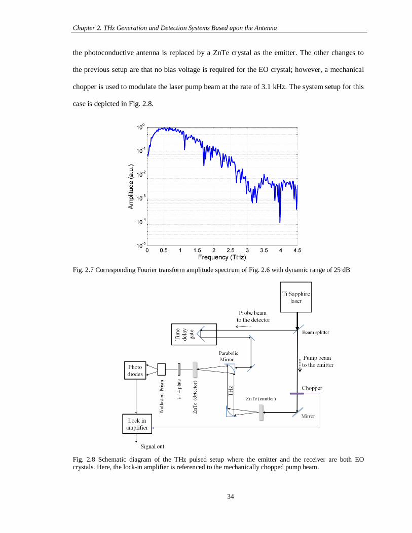
the photoconductive antenna is replaced by a ZnTe crystal as the emitter. The other changes to
the previous setup are that no bias voltage is required for the EO crystal; however, a mechanical
chopper is used to modulate the laser pump beam at the rate of 3.1 kHz. The system setup for this
case is depicted in Fig. 2.8.
Fig. 2.7 Corresponding Fourier transform amplitude spectrum of Fig. 2.6 with dynamic range of 25 dB
Fig. 2.8 Schematic diagram of the THz pulsed setup where the emitter and the receiver are both EO crystals. Here, the lock-in amplifier is referenced to the mechanically chopped pump beam.
Chapter 2. THz Generation and Detection Systems Based upon the Antenna
35
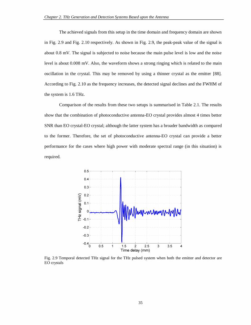
The achieved signals from this setup in the time domain and frequency domain are shown
in Fig. 2.9 and Fig. 2.10 respectively. As shown in Fig. 2.9, the peak-peak value of the signal is
about 0.8 mV. The signal is subjected to noise because the main pulse level is low and the noise
level is about 0.008 mV. Also, the waveform shows a strong ringing which is related to the main
oscillation in the crystal. This may be removed by using a thinner crystal as the emitter [88].
According to Fig. 2.10 as the frequency increases, the detected signal declines and the FWHM of
the system is 1.6 THz.
Comparison of the results from these two setups is summarised in Table 2.1. The results
show that the combination of photoconductive antenna-EO crystal provides almost 4 times better
SNR than EO crystal-EO crystal; although the latter system has a broader bandwidth as compared
to the former. Therefore, the set of photoconductive antenna-EO crystal can provide a better
performance for the cases where high power with moderate spectral range (in this situation) is
required.
Fig. 2.9 Temporal detected THz signal for the THz pulsed system when both the emitter and detector are
EO crystals
Chapter 2. THz Generation and Detection Systems Based upon the Antenna
36
Fig. 2.10 Corresponding Fourier transform amplitude spectrum of Fig. 2.9 with dynamic range of 18 dB
Table 2.1 Comparison of two THz systems based on various emitters whilst the detector is fixed
Emitter - Detector SNR
(linear scale)
FWHM BW
(THz)
Photoconductive antenna - EO crystal ~ 420 ~ 1
EO crystal - EO crystal ~ 100 ~ 1.6
2.5.2. Comparison of Ultra-Wideband THz Systems
There are more combinations that THz photoconductive antennas and EO crystals may be
used in THz pulsed systems. For example; Cai et al. compared the two systems based on EO
sampling and photoconductive sampling detection in the range of 0.1-3 THz when the emitter
was the same. Their results showed that the achieved signal from EO detection extended beyond
3 THz with slow roll-off whilst the one from photoconductive antenna had a cut-off at 2 THz.
From SNR point of view at low pump power modulation frequency, photoconductive sampling
outperforms the EO sampling; however, by increasing the modulation frequency (above 1 MHz to
overcome laser noise impact) both methods have almost the same SNR [89]. Similar reduction in
the bandwidth of the system based upon photoconductive sampling compared to the one with EO
Chapter 2. THz Generation and Detection Systems Based upon the Antenna
37
sampling was reported by Park et al. [88]. More recently, both an EO crystal and a large-aperture
THz photoconductive antenna have been used in emission side whilst the detector is an EO
crystal. Due to constructive superposition of the pre-generated THz wave from the EO crystal
with that of the antenna, detected THz signal enhanced almost twice of the only antenna case as
the emitter. Nevertheless, there was a slight improvement in the detected bandwidth [90]. These
efforts highlight the importance of the type of emitter and detector devices in a THz pulsed
system. Therefore, selecting the appropriate THz emitter and detector for any desired THz
application is an important issue, and the discussion based on performance of the each system is
useful for choosing the suitable combination (of EO crystal and photoconductive antenna) when
setting up a THz generation and detection system. Next, the merits of four different systems
where the laser source has ultra-short laser pulses (smaller than 20 fs) are discussed. The use of
published results will be cited as examples in order to supplement this comparison [91].
Case A: Emitter: EO crystal, Detector: EO crystal
Wu et al. [92] reported a spectral range as wide as 37 THz by using a 450-μm-thick GaAs
crystal as the emitter, a 30-μm-thick ZnTe crystal as the receiver, and 12 fs laser pulses. In a
further study, Huber et al. [71] demonstrated that, when both the emitter and receiver are thin EO
crystals, a spectral range as broad as about 41 THz can be obtained, using a 10 fs laser system.
These ultra-wideband spectral ranges are desirable for the experiments of condensed matter
physics. However, these systems generally provide a lower emission power and smaller peak
electric fields as compared to those of THz photoconductive antennas [77]. If phase matching in
EO crystals is satisfied, the average detected power from this setup can be improved [93].
Case B: Emitter: EO crystal, Detector: THz photoconductive antenna
This case was investigated by Kono et al. [86]. The emitter was an SI-InP crystal, excited
by 15 fs laser pulses. The receiving side employed a 30-μm-long dipole antenna with a 5-μm-long
gap between the electrodes, fabricated a GaAs substrate, and embedded on a Si lens to enhance
the THz collection efficiency. The detected spectral range was beyond 20 THz; however, there
Chapter 2. THz Generation and Detection Systems Based upon the Antenna
38
were some dips in the frequency response. The dips from 7 to 9 THz were attributed to the GaAs
phonon resonance, and at 15.5 THz the absorption was related to the Si lens. It has been observed
that the material property of the antenna influences the useful spectral range of the THz system.
Moreover, it has been illustrated that spectral range can be broadened to almost 50 THz when the
emitter changed to ZnTe crystal and the same photoconductive antenna detector positioned in the
reverse direction [94]. Changes in emitter crystal resulted in phonon absorption in frequencies of
5.3 THz and 10.56 THz. Also, by using the antenna in the reverse direction, both the THz
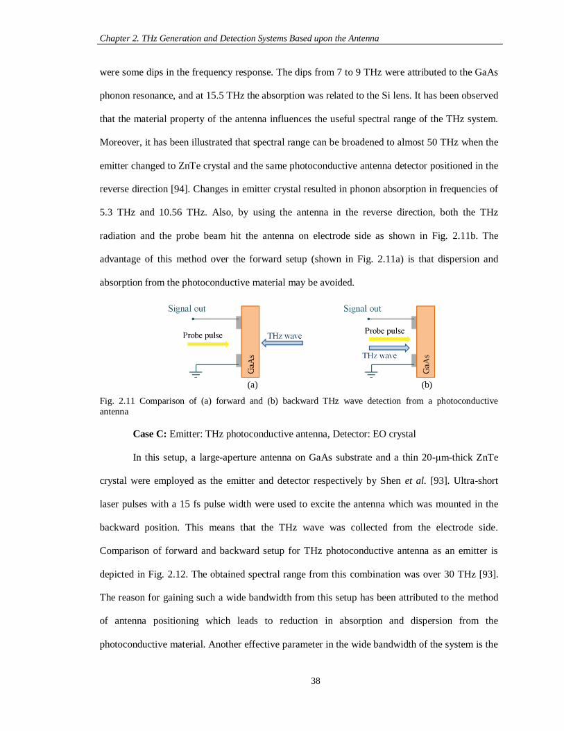
radiation and the probe beam hit the antenna on electrode side as shown in Fig. 2.11b. The
advantage of this method over the forward setup (shown in Fig. 2.11a) is that dispersion and
absorption from the photoconductive material may be avoided.
(a) (b)
Fig. 2.11 Comparison of (a) forward and (b) backward THz wave detection from a photoconductive
antenna
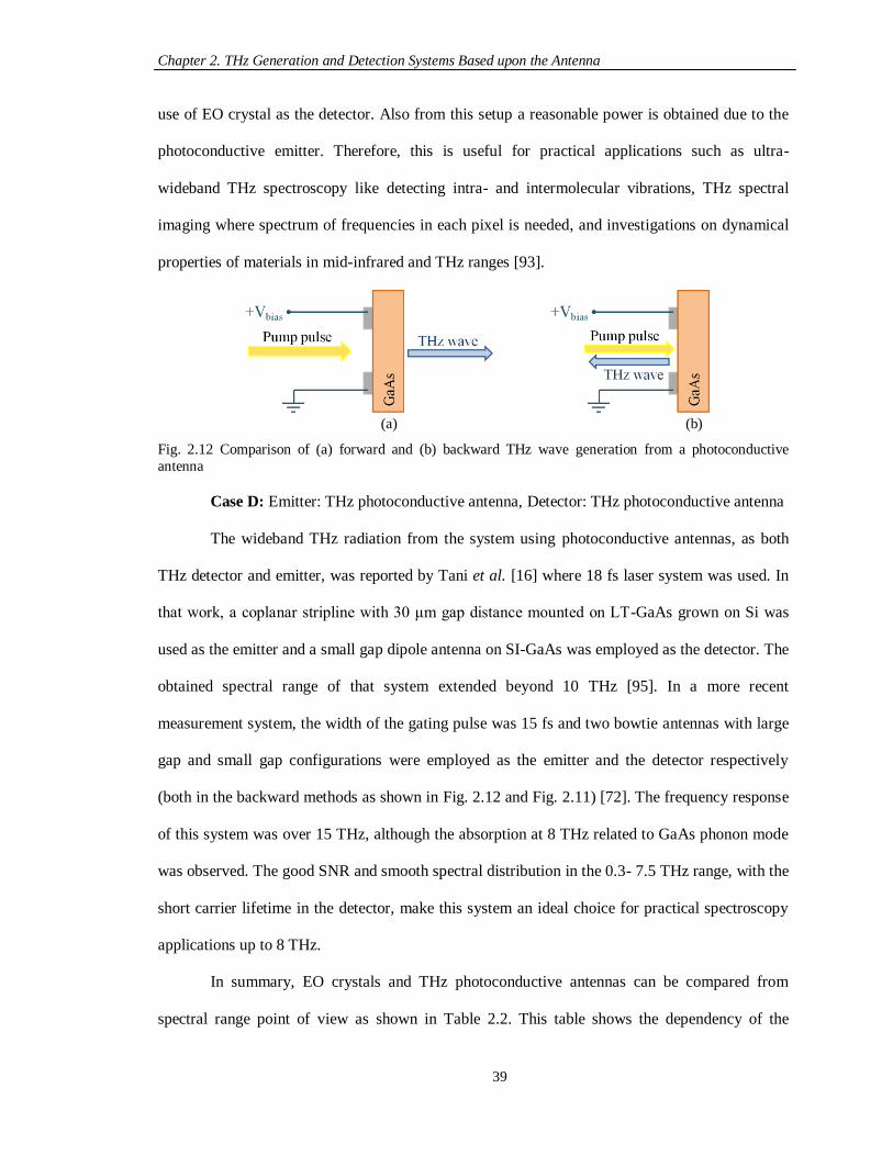
Case C: Emitter: THz photoconductive antenna, Detector: EO crystal
In this setup, a large-aperture antenna on GaAs substrate and a thin 20-μm-thick ZnTe
crystal were employed as the emitter and detector respectively by Shen et al. [93]. Ultra-short
laser pulses with a 15 fs pulse width were used to excite the antenna which was mounted in the
backward position. This means that the THz wave was collected from the electrode side.
Comparison of forward and backward setup for THz photoconductive antenna as an emitter is
depicted in Fig. 2.12. The obtained spectral range from this combination was over 30 THz [93].
The reason for gaining such a wide bandwidth from this setup has been attributed to the method
of antenna positioning which leads to reduction in absorption and dispersion from the
photoconductive material. Another effective parameter in the wide bandwidth of the system is the
Chapter 2. THz Generation and Detection Systems Based upon the Antenna
39
use of EO crystal as the detector. Also from this setup a reasonable power is obtained due to the
photoconductive emitter. Therefore, this is useful for practical applications such as ultra-
wideband THz spectroscopy like detecting intra- and intermolecular vibrations, THz spectral
imaging where spectrum of frequencies in each pixel is needed, and investigations on dynamical
properties of materials in mid-infrared and THz ranges [93].
(a) (b)
Fig. 2.12 Comparison of (a) forward and (b) backward THz wave generation from a photoconductive
antenna
Case D: Emitter: THz photoconductive antenna, Detector: THz photoconductive antenna
The wideband THz radiation from the system using photoconductive antennas, as both
THz detector and emitter, was reported by Tani et al. [16] where 18 fs laser system was used. In
that work, a coplanar stripline with 30 μm gap distance mounted on LT-GaAs grown on Si was
used as the emitter and a small gap dipole antenna on SI-GaAs was employed as the detector. The
obtained spectral range of that system extended beyond 10 THz [95]. In a more recent
measurement system, the width of the gating pulse was 15 fs and two bowtie antennas with large
gap and small gap configurations were employed as the emitter and the detector respectively
(both in the backward methods as shown in Fig. 2.12 and Fig. 2.11) [72]. The frequency response
of this system was over 15 THz, although the absorption at 8 THz related to GaAs phonon mode
was observed. The good SNR and smooth spectral distribution in the 0.3- 7.5 THz range, with the
short carrier lifetime in the detector, make this system an ideal choice for practical spectroscopy
applications up to 8 THz.
In summary, EO crystals and THz photoconductive antennas can be compared from
spectral range point of view as shown in Table 2.2. This table shows the dependency of the
Chapter 2. THz Generation and Detection Systems Based upon the Antenna
40
radiated THz field and detected THz signal on the frequency for each of these devices when
employed as the emitter and detector.
The spectral range of THz pulsed systems based upon the combination of aforementioned
devices as “Emitter-Detector” can be estimated by multiplication of their transfer functions which
are as a function of the frequency.
Table 2.2 Dependency of THz signal to frequency based on the emitter and detector type
Component Emitter Detector
EO crystal fETHz [80] Detected signal 1
THz Photoconductive
antenna
1THzE
Ultra short carrier lifetime: Detected signal1
Long carrier lifetime: Detected signal f/1
Therefore, the comparison of the spectral range of these systems as a combined “Emitter-
Detector” can be presented as:
EO crystal- EO crystal > EO crystal- THz photoconductive antennas > THz
photoconductive antennas- EO crystal > THz photoconductive antennas- THz photoconductive
antennas
In other words, the system with EO crystals as both the emitter and detector has the
largest spectral range, and the system with THz photoconductive antennas has the smallest
spectral range.
In photoconductive antennas, the dominant noise is Johnson noise or thermal noise1 and
for a good SNR detection, photoconductive materials with a short carrier lifetime on the detector
side are preferable. To elaborate further, thermal noise is proportional to the square root of
conductivity of photoconductive material [85]. Considering the relation of conductivity with the
carrier lifetime and mobility, the noise level on detector side, Inoise, is proportional to [96]:
1 Another type of the noise in THz systems is the laser shot noise which is proportional to the
square root of detected THz current (or the laser power) [77].
Chapter 2. THz Generation and Detection Systems Based upon the Antenna
41
cenoiseI . This demonstrates that antennas with long-lived and high mobility
photoconductive materials have poor SNR.
Comparison of THz pulsed systems from SNR point of view is not very straight forward
because this factor is a very practical parameter and it depends mainly on laser and experimental
situation such as system alignment. However, in general systems based upon THz
photoconductive antennas as emitters have larger THz electric field amplitude than the EO
crystals [3, 72]. From component combination point of view, at low frequencies combination of
THz photoconductive antennas-THz photoconductive antennas have better SNR than THz
photoconductive antenna-EO crystal and EO crystal-EO crystal [72, 88]. At high frequencies like
30 THz, set of EO crystal-EO crystal performs better than THz photoconductive antenna-THz
photoconductive antenna from SNR point of view due to sensitivity reduction of the
photoconductive antennas at high frequencies.
Therefore, considering application requirement; i.e. whether high power THz pulsed
system is required or a system with a broad bandwidth and also considering losses due to
absorption in special frequencies in antenna substrate material and EO crystal, a combination of
these devices can be used. If we want good SNR with smooth spectral range and moderate
spectral range, a combination of THz photoconductive antenna-THz photoconductive antenna can
be the appropriate choice. If we want a system with high radiated power and broad spectral range,
the set of THz photoconductive antenna-EO crystal can be a good option. Moreover, considering
1) different characteristic requirements for each of these components and 2) various factors that
contribute in generation and detection of THz signals from them as an emitter and detector (i.e.
for THz photoconductive antenna as an emitter, effective factors are the pump laser and the bias
field whilst as a detector the probe pulse and radiated THz field are effective parameters), it
cannot be concluded that a system combining EO crystal as an emitter-THz photoconductive
antenna as a detector has the same performance as THz photoconductive antenna as an emitter-
Chapter 2. THz Generation and Detection Systems Based upon the Antenna
42
EO crystal as a detector . Furthermore, if emitter and detector antennas have photoconductive
materials with different characteristics such as carrier lifetime (due to for instance, usage of
different photoconductive materials or variation in fabrication procedure for the same
photoconductive material) and their place is exchanged within the experimental setup, the
detected signal will be different [85]. Last but not least, these comparisons and analyses provide
an overview of different setup combinations, and this is helpful in selecting a THz
photoconductive antenna and EO crystal as an emitter and a detector in a THz pulsed system.
2.6. The THz CW Systems
THz pulsed systems are based on expensive femtosecond laser systems; however, for
long term industrial operation they are not stable and reliable enough [97]. Also, they have issues
in generation of narrow linewidth spectral data [66]. Therefore, a suitable alternative option is the
THz CW systems; this is a coherent method same as the THz pulsed system and it can offer a
better resolution on a pre-selected linewidth. A THz CW measurement system based on THz
antennas using two CW Ti:sapphire lasers was first employed by Verghese et al. [98]. In THz
CW systems, an antenna is always employed as the emitter (whether it is the reference antenna or
the antenna under test). On the detection side, a THz photomixer antenna [65, 66] and a
bolometer or Golay cell [99-101] are two commonly used methods (former is the coherent
method and the latter is the incoherent one). The schematic of a THz CW system using a
bolometer as a detector is shown in Fig. 2.13.
Two single mode laser pulses are made collinear and combined through a beam splitter
and then the resulting beam is focused on the THz photomixer antenna. THz wave is coupled to
the air through the antenna substrate and it is detected by a bolometer. The bias voltage of the
antenna is used as the reference for the lock-in detection. The optical frequencies of laser beams
may be varied by tuning of the laser cavity length [98], changing the operating temperature [99]
or use of optical grating structures [102]. In this thesis, a THz CW system for characterisation of
Chapter 2. THz Generation and Detection Systems Based upon the Antenna
43
the new antenna design is employed. More details are described in Chapter 7.
Fig. 2.13 Schematic diagram of a common THz CW system
Each of the THz pulsed systems and CW systems has advantages and disadvantages.
Table 2.3 is a summarised comparison of them.
Table 2.3 Comparison of THz pulsed and CW systems
THz pulsed system THz CW system
Type of system
System complexity
Broadband1
High
Narrowband
Low
System weight Heavy and bulky Light and compact
Laser source Femtosecond lasers Laser diodes
System cost [103] ~ 6A* A*
Spectroscopic information
Broadband and enormous amount
of information
Limited information
Depth of imaging information [59] Good Poor
*A shows the amount of money.
1 The upper limit of achievable bandwidth is determined by the femtosecond laser pulse duration.
Chapter 2. THz Generation and Detection Systems Based upon the Antenna
44
In Fig. 2.14, the sources of these systems are depicted for size comparison. It shows that
optical sources for CW systems are considerably smaller than those for pulsed systems.
Another recent type of THz systems is the THz quasi time domain spectroscopy (QTDS)
which is based upon an inexpensive and commercially available multimode laser diode [97]. In
this technique, equidistant frequency spacing of the laser modes results in pulses like the ones
from a THz pulsed system. Thus, this method combines advantages of both pulsed and CW
systems. In other words, it has a relatively broad bandwidth (the first reported system showed 600
GHz bandwidth [97]) and the optical source is cheap. This can be a suitable option for affordable
commercial applications.
(a) (b) (c)
Fig. 2.14 Size comparison of laser sources for THz systems (a) Ti: Sapphire laser with an external power
supply and a separate chiller compound for pulsed systems, dimensions of pump laser is 152.4 × 60.9 ×
23.6 cm [104] (b) the world most compact Ti: Sapphire laser with dimensions of 22.5 × 22.5 × 6.2 cm
[105] (c) laser diode for CW systems with dimensions of 1.2 × 0.9 × 0.7 cm [106]
2.7. Summary
A THz antenna is one of the main components of THz systems. It can be employed as an
emitter and/or detector. The required background on major THz systems including THz pulsed
systems and THz CW systems were reviewed. In THz pulsed systems, an EO crystal is another
common component that may accompany the antenna. Hence, the working principles and features
of both EO crystals and photoconductive antennas were explained. The performance of two THz
pulsed systems based upon the combination of THz photoconductive antenna-EO crystal and EO
crystal-EO crystal as the emitter-detector were measured and compared from bandwidth and SNR
Chapter 2. THz Generation and Detection Systems Based upon the Antenna
45
point of view. Since laser pulse duration has a crucial effect on the bandwidth of detected THz
signal, merits of four different THz systems employing an EO crystal and a THz photoconductive
antenna for ultra-short laser pulse duration (< 20fs) were reviewed. Finally, THz pulsed systems
and CW systems were compared from various aspects. Working principle and requirements of
THz antennas in THz systems depend on the entire system and the position that the antenna is
used (emitter and/or detector). Thus, the presented measurement, comparison and analysis in this
chapter have provided a useful summary on characteristics of each setup. This aids understanding
differences of each combination and choosing the appropriate one for the practical application.
Chapter 3. THz Antennas
3.1. Introduction
After studying various THz systems, in this chapter the investigation is narrowed down to
the specific part: the THz antenna. As emitters, it converts optical waves to THz waves. In the
detector side, it transforms THz energy to electric energy detectable by a lock-in amplifier. As
described in Chapter 2, in both THz pulsed and CW systems (for the case of THz antenna-THz
antenna as the emitter-detector combination), the THz antenna is the final block on the emission
side, and it is the first block on the detection side. Hence, it is a fundamental and essential
component of a THz system. However, special excitation method of this antenna imposes new
and different approaches for antenna analysis, simulation, fabrication and measurement as
compared to a common RF/MW antenna. Thus, in this chapter after highlighting the necessity of
having an antenna, THz antennas are compared with RF/MW antennas. This comparison is very
important because it highlights research options in THz antennas and it builds the base for
contributions of this thesis. The main challenges in development of THz systems and THz
antennas are the low output power of the system and the small optical-to-THz efficiency. In order
to analyse these problems and find out the reasons, a new approach is adopted; in which the
optical-to-THz conversion efficiency from both THz photoconductive and photomixer antennas
are shrunken to three distinct processes. Then based on the requirement for THz antennas, the
main parameters affecting the radiated power and optical-to-THz conversion efficiency are
Chapter 3. THz Antennas
47
summarised in a simplified block diagram. Along with each parameter, that is stated in this
diagram, available techniques and mainly antenna solutions are introduced and studied from
literature. Finally, some antenna geometries for various THz applications are reviewed.
3.2. Necessity of Having a THz Antenna in a THz System
THz waves can be generated in bulk, unbiased semiconductor materials like InP and
GaAs as in the observation of surface field THz emission [107, 108]. Under illumination by
femtosecond optical pulses, electron-hole pairs on the surface of the semiconductor substrate are
separated and polarised perpendicularly to the surface of the semiconductor. Then, due to
acceleration of the carriers in the electric field originating in the surface depletion layer of the
semiconductor a THz wave is radiated [109]. Carrier mobility and the intensity of the static
internal field affect the amplitude and phase of the radiated THz field [107]. Applying an external
magnetic field enhances THz emission from semiconductor surfaces and this is because of the
reorientation of the created dipole in semiconductor towards the surface [110]. Nevertheless, the
emitted power based on this method is small. This can be improved by employing antenna
electrodes on the semiconductors’ surface and by applying an external bias field across the
antenna which surpasses the surface depletion field [111]. Therefore, the THz antenna plays a
very important role in stronger THz generation and detection. In recent years, THz antennas (both
photoconductive and photomixer types) are commercially available from companies such as
Menlosystem [112], Tetechs [113], Toptica [114] and Thorlabs [115].
3.3. Comparison of THz Antennas with RF/MW Antennas
Working principles of THz photoconductive antennas were described in Chapter 2.
Measurement setups of common RF/MW and THz photoconductive antennas are respectively
shown in Fig. 3.1a and Fig. 3.1b. It is apparent that THz antennas based upon laser excitation,
which are excited by the laser optical source, are very different from the conventional RF/MW
Chapter 3. THz Antennas
48
antennas from the feeding, measurement facility, and antenna structure points of views. In this
section, these differences are elaborated and summarised [116, 117].
(a)1
(b)
Fig. 3.1 Common (a) RF/MW antenna (b) THz antenna measurement setup (both the emitter and detector
are antennas)
3.3.1. Excitation Source, Feeding and Biasing
Various feed lines are available for conventional antennas such as coaxial cable,
microstrip, and CPW; but, there is no analogous feed line for a THz antenna in reality. In fact,
1 It is possible to test THz antennas (the ones that do not require optical excitation) by using vector
network analyzers (for instance network analyzers by Agilent can measure up to 1.1 THz). However, the
focus of this thesis is on the THz antennas with optical excitation and the provided discussion in this
section covers comparison between this type of THz antennas and common RF/MW antennas.
Chapter 3. THz Antennas
49
there are two ways to couple the optical pulses to a THz antenna; one is through the air and the
other one is through a fibre. In common THz time domain setups as explained in Chapter 2,
optical waves are coupled to the antenna through the air. However, for some industrial
applications flexible and movable emitters and detectors are an asset and this can be achieved by
employing optical fibres. Recently some fibre-coupled THz systems have been presented for 800
nm laser pulses [118] and 1550 nm (telecom wavelength) pulses [119, 120]. Nevertheless, the
feed line for THz antennas is actually a laser beam; therefore, the source impedance of the
antenna is variable and this is very distinct to commonly 50 Ohms feed lines of RF/MW antennas.
This imposes a requirement for new method of analysis for THz antennas which is one of the
main scopes of this thesis, and it is investigated in Chapter 4.
Another difference between RF/MW and THz antennas is from bias voltage point of
view. RF/MW antennas do not need any biasing1. However, as depicted in Fig. 3.1b THz
antennas as emitters require biasing because it is the fundamental procedure of THz generation.
THz antennas do not require bias voltage when they are employed on detection side.
3.3.2. Substrate Material
In planar RF/MW antennas, antenna substrate must be a low-loss dielectric material. One
of the most common dielectric materials for this type of antennas is FR4, which consists of
fibreglass reinforced epoxy laminate sheet. For a special MW antenna category, i.e. monolithic
microwave integrated circuit (MMIC), GaAs is the main substrate material due to its high carrier
mobility [12, 121]. In all THz antennas, the substrate is a photoconductive material which is
basically a semiconductor, such as Si, GaAs, and InGaAs. LT-GaAs is the most popular material
due to its desirable characteristics, namely ultra-short carrier lifetime (to get fast current pulses or
CW current variation), relatively high electron mobility (to get strong THz signals), high intrinsic
1 Some RF/MW antennas like the ones based upon RF-MEMS switches and p–i–n diodes require
biasing.
Chapter 3. THz Antennas
50
resistivity and high breakdown voltage (to support applying high bias voltages) [122, 123]. Since
photoconductive materials play an important role in THz wave generation and detection,
characteristics and effective parameters of them with the main focus on LT-GaAs is described in
the next sub-section.
Another substrate related difference between THz antennas and RF/MW antennas is the
substrate thickness. In THz antennas, the substrate thickness becomes comparable to the radiated
THz wavelength; hence, guided waves in the substrate need to be taken into account. This issue is
explored in Chapter 6.
3.3.2.1. THz Photoconductive Materials
THz photoconductive material is one of the intensely studied topics in the THz field. The
main reason is that, no naturally occurring material exists which allows an efficient and powerful
THz emission [124]. The intrinsic carrier lifetime of materials is not fast enough to reach very
high frequency ranges of THz spectrum. Thus, to reduce the carrier lifetime, material studies for
THz are very crucial, and research and improvement of material characteristics for optoelectronic
applications still continues [125, 126].
Silicon was employed as the photoconductive substrate material in the first THz antenna
developed by Auston [68]. The bandgap of silicon is 1.12 eV at 300 K, with corresponding
intrinsic resistivity of 2.3 × 10⁵ Ω.cm. However, the bandgap of silicon is indirect which means
that the minimum of conduction-band is misaligned compared to the maximum of valence-band
[127]. Thus, optical recombination processes are relatively slow. In contrary, GaAs has a direct
bandgap and photon emission is possible without phonon exchange with the lattice. The intrinsic
resistivity of GaAs is 108 Ω.cm. Moreover, GaAs is an III-V compound; therefore, it is possible
to modify the composition of alloys by adding defects to tune the electrical and optical
behaviours. Indeed development in characteristics of GaAs is one of the main reasons that has
made possible the steady progress of THz antennas [128].
Chapter 3. THz Antennas
51
GaAs crystal can be grown in semi-insulating (SI) form by the liquid encapsulated
Czochralski (LEC) method. In this process, all dependencies of GaAs on quartz and carbon
components are eliminated [129]. This forms a substrate where it is possible to grow another
epitaxial layer. The carrier life time of SI-GaAs is in the range of hundreds of picoseconds. In
order to have THz antennas with large bandwidth and good SNR, the carrier lifetime needs to be
very small. This may be achieved by incorporating additional energy levels in the bandgap
through various native point defect types (i.e. arsenic antisites AsGa and gallium vacancy point
defects VGa) [122]. Therefore, another recombination path can be provided by trapping electrons
in intermediate states. For this purpose, point defects should be introduced into the crystal.
Adding defects can reduce carrier lifetime of the material which is desirable. On the other hand, it
reduces thermal conductivity and the carrier mobility because the mean free path is decreased as a
result of new scattering centres introduced by trapping levels [81, 130]. These consequences are
unfavourable. Thus, the main challenge in the development of ultrafast photoconductive materials
is to have a material with sub-picoseconds carrier lifetime, a usefully high mobility, and a high
dark resistivity simultaneously. Nevertheless, commonly the priority is given to the short carrier
lifetime characteristic and adding defects is the dominant method for THz material fabrication.
There are various methods for introducing defects into the material, and a popular one is
the low temperature molecular beam epitaxy (MBE). LT-GaAs is produced through this
technique. In this method, GaAs is deposited at low growth temperature (typically between 200 to
250°C) in excess of As which leads to the formation of a relatively high density of point defects.
After that, it is annealed under an As overpressure at high annealing temperature (typically
between 500 and 600°C) [123, 131] to increase the resistivity. Usually a 1 to 2 μm-thick LT-
GaAs layer as the active layer is grown on SI-GaAs [122]. LT-GaAs was first used by Smith et
al. in 1988 as a substrate of a THz photoconductive antenna [87] and since then overwhelming
research on the effect of various growth and annealing factors on properties of LT-GaAs has been
performed [131-134]. However, still in the literature when a THz antenna on LT-GaAs is used the
Chapter 3. THz Antennas
52
full parameters, related to the production of the LT-GaAs (growth and annealing temperatures)
wafer and the derived carrier lifetime, are stated. The reason is that each MBE chamber is unique
and even in a same chamber it is very difficult to reproduce the wafer with the same
characteristics from one time to the next. This is because of the sensitivity of the fabrication
process to the ambient condition and difficulty in controlling the exact growth temperature. A
literature survey of the carrier lifetime versus the growth temperature is collected in Fig. 3.2. This
shows the broad range of carrier lifetime values for LT-GaAs which is the result of the
inconsistency between growth facilities. Yet it can be observed that the carrier lifetime of LT-
GaAs is very short and this is because very fast carrier lifetime at localised defect sites created in
the fabrication process. Another parameter of the photoconductive material influenced by the
fabrication procedure is the material resistivity. By increasing the growth temperature the
resistivity decreases [135]; however, the annealing process helps to increase the resistivity again.
Fig. 3.2 Measured carrier lifetime of LT-GaAs as a function of growth temperature from references [86, 96,
123, 135-138]
It is good to add that other techniques to modify characteristics of GaAs have been
practiced like ion-implantation [96] and self-assembled ErAs islands in GaAs [128, 139, 140].
These methods can lead to a substrate material with the similar carrier lifetime to that of LT-
Chapter 3. THz Antennas
53
GaAs. Ion-implanted GaAs has high mobility but with very low intrinsic resistivity and
ErAs:GaAs has high resistivity but with low mobility. Therefore, LT-GaAs still provides the best
material characteristics for THz antennas [124].
Another category of photoconductive materials for THz applications is the Indium based
III-V compounds. These materials have narrower bandgap energy; for instance, bandgap of
InGaAs is 0.75 eV compared to 1.43 eV of LT-GaAs. Thus, Indium based III-V compounds are
suitable materials at high optical wavelengths (but their dark resistivity is low which is associated
with their low bandgap energy). Same as LT-GaAs, a thin layer of InGaAs is grown on InP (the
lattice-matched material for InGaAs). At optical wavelengths such as 1.06 μm, LT-InGaAs
material with ultra-short carrier lifetime and high resistivity has been reported [126]; however,
main interest on InGaAs is for the telecom wavelength of 1.55 μm. The advantage of this
wavelength is that the lasers are cheaper and less bulky than lasers at 800 nm wavelength. In
addition, in this wavelength well developed fibre technology can be employed. Fibre amplifiers
with high power, narrow line-width and tunable wavelength in this frequency are also available
[141]. Compatibility with 1.55 μm has been achieved with Fe-implanted InGaAs [142, 143],
ErAs:InGaAs [144], heavy-ion irradiated InGaAs [145], embedded InGaAs layers between
InAlAs trapping layers [119], and low-temperature-grown Be doped InGaAs [146].
As a summary, the properties of different main THz photoconductive materials for
optical sources of 800 nm (SI-GaAs and LT-GaAs) and 1.55 μm (LT-InGaAs) are shown in Table
3.1. The advantage of SI-GaAs is its high mobility; however, since it has lower breakdown field
compared to LT-GaAs the amount of applied dc bias field for THz antennas based on SI-GaAs is
limited. In addition, its lower resistivity results in generation of larger dark current (when there is
no laser illumination) in comparison to LT-GaAs which leads to heating of the device and quicker
break down than LT-GaAs. Another issue of the SI-GaAs is its large carrier lifetime which limits
the achievable spectral range and it leads to the more noise. For InGaAs, there are various
fabrication techniques which subsequently lead to variation in the characteristic of the material.
Chapter 3. THz Antennas
54
For LT-InGaAs, the carrier lifetime, resistivity, and breakdown field at 1550 nm are very low.
However, the greatest advantage of this material is that it can be used with well established
communication optical sources; this can reduce the cost of THz system considerably. In general,
LT-GaAs is the most popular photoconductive material for THz applications because of its
excellent combined features.
Table 3.1 Properties of various photoconductive materials in THz antennas
LT-InGaAs Larger than LT-GaAs[149] 26 [146] 1 760 [146]
1 ~ 6×10
4 [146]
1
3.3.3. Antenna Electrode Material
RF/MW antennas are usually made with highly conductive metals such as copper. In
MMIC technique, gold metallization is used for transmission lines. In THz antennas, an AuGe
alloy and a layer of Ti/Au (Titanium/Gold) are employed as the electrode material. These are
suitable metallization types on LT-GaAs substrates and can provide ohmic contacts2 [150]. AuGe
alloys such as AuGe/Ni/Au have been used in THz antennas [69, 99]. However, Ti/Au (or
Ti/Pd/Au) layer stack is more extensively employed [72, 90, 98, 111] where a thin layer of Ti is
initially deposited to improve adhesion of the Au to the substrate [12]. The advantage of the
Ti/Au contact over the AuGe alloy is that, after its deposition, no annealing is required and it is
more thermally stable under laser illumination [150].
The electrical conductivity, σ, of Au is 45.2 × 10⁶ S/m [2]. The skin depth or
1 This is for LT- Be doped In0.45Ga0.55As which improves resistivity of LT-InGaAs considerably. 2 The I-V curve of the device is linear.
Chapter 3. THz Antennas
55
characteristic depth of penetration, f1 , for Au at 1 THz is 74.9 nm. Thus, most of
current flow occurs in a very thin region near the surface of the conductor. In this case, the
surface resistance of a gold slab with an equal width and length size, by using )(1 depthR , is
0.29 Ω. In practice for THz antennas, usually 10-20 nm thick Ti followed by Au with thickness of
more than few tens of nm is deposited on the photoconductive substrate.
Another type of material, which very recently has been theoretically studied as an
antenna electrode material, is graphene [151, 152]. It is a one-atom-thick 2D carbon crystal which
has extraordinary mechanical, electronic and optical properties [153]. It has a Young modulus of
1.5 TPa, carrier mobility of 200 000 cm2.V
-1.s
-1 [154] and an absorption coefficient of 24×10
4 cm
-
1 [155]. The surface conductivity of graphene depends on various parameters such as temperature
and chemical potential. Chemical potential is one of the parameters which can be tuned to achieve
antennas with different radiation characteristics; i.e. reconfigurable antennas [156].
3.3.4. Type of Current
In RF/MW antennas, the current type is the conduction current which is due to the motion
of conduction electrons. In THz antennas generation of current in the photoconductive material is
attributed to two phenomena: 1) Generation of electron-hole pairs under electric bias field known
as drift current 2) Displacement current which is due to second order nonlinear optical
characteristics of the photoconductive substrate. However, the effect of displacement current is
only considered at low bias fields. At high bias fields (more than 105 V.cm
-1), drift current is
dominant [78, 157].
3.3.5. Fabrication and Measurement
Fabrication of a THz antenna is a complicated and expensive task due to small size of the
device and requirement of special fabrication environment. Manufacturing of a THz antenna
consists of 1) fabrication and preparation of the photoconductive substrate and 2) patterning the
Chapter 3. THz Antennas
56
antenna on the substrate. The substrate preparation part was briefly explained in section 3.3.2. For
the second part, depositing the metal part of THz antenna on the photoconductive substrate, two
ways of photolithography and electron beam lithography are used. The latter method, which is
more expensive than the former one, is employed for sub-micron dimensions that fall below the
resolution of photolithography method.
From measurement setups and measurement techniques points of views, these two types
of antennas are also very different. In RF/MW antennas as illustrated in Fig. 3.1a, both
transmitter (TX) and receiver (RX) antennas are connected to a vector network analyzer and then
various parameters of the antenna under test can be determined. Anechoic and reverberation
chambers are commonly used measurement facilities1. In the THz measurement setup, which are
based upon the laser excitation sources, as shown in Fig. 3.1b, there is no physical connection
between the optical source and the emitter and/or detector antenna2. Various optical components,
such as parabolic mirrors, are allocated between the emitter and detector antennas to direct the
electromagnetic wave which may attenuate and broaden the THz signal. From the depicted setup
in Fig. 3.1b, the amplitude and phase of the THz signal can be detected. In THz antennas based
upon photoconduction technique, for THz wave generation and/or detection, the antenna should
be illuminated by the laser source all the time, i.e. misalignment between the antenna and the
optical source affects the THz wave generation and/or detection. Therefore, for antenna pattern
measurement another measurement setup, such as using fibre coupled detectors, is needed [158,
159]. This assures that the antenna under test in the THz system does not lose laser illumination;
therefore, the pattern of the antenna can be evaluated without any interruption. Last but not least,
since THz signals are sensitive to water vapours, so a THz measurement bench is typically
enclosed and purged in dry nitrogen.
1Required measurement methods and facilities are determined based upon the antenna type and
size [1] 2 If fibre coupled systems are used, the antenna is connected to the source through an optical fibre.
Chapter 3. THz Antennas
57
3.3.6. Computer Aided Design
Computer Aided Design (CAD) is now a common practice for conventional antenna
designs; but, there is no one complete design tool available for THz antenna designs. In other
words, generation of THz waves from the antennas consists of two processes 1) optoelectronic
and 2) electromagnetic (EM) parts. The available commercial tools can only simulate the first or
second part of the process. Hence, the development of a new method that can facilitate analysis of
THz antennas by combining numerical and CAD methods is required. This is one of the
contributions of this thesis that will be explained in Chapter 6.
To sum up, the major differences between these two types of antennas are reviewed in
Table 3.2 (the exceptions were previously elaborated). The dissimilarities highlight necessity of
having different analysis approach for THz antennas.
Table 3.2 Comparison of THz antennas with common RF/MW antennas
Parameter THz antenna RF/MW antenna
Excitation source/feeding Laser pulses Transmission line
Bias voltage Emitter: biased
Receiver: unbiased
Emitter: unbiased
Receiver: unbiased
Substrate material High resistive semiconductor Low loss dielectric
Antenna electrode material AuGe and Ti/Au Highly conductive metals
Type of current Drift current and displacement
current
Conduction current
Fabrication Complex and expensive Larger availability of
fabrication facilities
Computer aided design Not available in one package Available
Chapter 3. THz Antennas
58
3.4. Problems of THz Antennas
Advantages and disadvantages of different THz sources were reviewed and described in
Section 1.2. Among all those various sources, THz antennas and EO crystals are the most
common devices as discussed in Chapter 2. Although other THz sources may have better THz
radiation performance in particular circumstances, THz antennas and EO crystals have gathered
various useful characteristics in one place. These components can operate in room temperature
(unlike QCLs), they are small (unlike BWOs), and they can operate over a wider range of THz
frequencies (unlike diodes). However, the radiated THz power and the optical-to-THz conversion
efficiency from them is very low [3].
In EO crystals, optical-to-THz conversion is inherently an inefficient process because of
the mismatching between the optical group velocity and THz phase velocity. Moreover, thickness
of the crystal is very important in wave absorption and amplitude of the radiated THz wave. In
order to mitigate the drawback of the absorption, high optical power sources need to be used to
generate meaningful THz powers [160]. Another restriction of this technique arises from the
Manley–Rowe rule which is about the conservation of power in a nonlinear optical process [161].
Thus, the ratio between the energies of the generated THz photon and the optical source photon
(i.e. the quotient of output THz and input optical frequencies) restricts the power efficiency of EO
crystals. On the whole, EO crystals usually provide lower output power than photoconductive
antennas in spite of their advantages on providing wider bandwidth [3].
THz wave generation through photoconduction process has shown promising
performance [128, 162-165]. One of the major advantages of THz antennas is that under a laser
illumination, for each absorbed photon by the photoconductive material one electron-hole pair is
generated and when this pair reaches the antenna several THz photons can be emitted [166]. In
practice, the radiated THz power is in the range of few μW and the optical-to-THz conversion
efficiency of THz antennas is very low (< 2%). In Fig. 3.3 and Fig. 3.4 a literature survey of
Chapter 3. THz Antennas
59
average THz output power versus the input optical power of several THz photoconductive and
photomixer antennas are respectively presented.
Fig. 3.3 Measured THz output power from a THz photoconductive antenna as a function of average input
optical power from references [69, 141, 160, 163, 164, 167, 168]
Fig. 3.4 Measured THz output power from a THz photomixer antenna as a function of average input optical
power at various single working frequencies from references [100, 131, 162, 169-173]
In order to have a better view and understand the reason of having a low power level and
efficiency, the entire wave generation process from a THz antenna needs to be considered. For
this purpose, the new approach and the adopted method here is to divide the process into three
Chapter 3. THz Antennas
60
parts:
1) Generation of THz photocurrent from optical power in the photoconductive material.
The related efficiency; i.e. optical-to-electrical efficiency, η1, can be defined as the ratio of the
generated THz power in the photoconductive gap or photomixer to the optical power
2) The amount of coupled THz power from the photoconductive gap to the antenna
electrodes; i.e. matching efficiency, η2
3) The amount of coupled THz wave from the antenna to the free space; i.e. radiation
efficiency, η3.
The first two parts are different for THz antennas in a pulsed and a CW system due to the
excitation type, and they are separately described in the next sections. However, the latter part;
i.e. radiation efficiency, for both systems is the same and it depends on the antenna radiation
characteristics- mainly the electrical thickness of substrate and the relative permittivity of
photoconductive material. Since the photoconductive substrate has high permittivity (εr = 12.9 for
GaAs), as substrate thickness increases, the radiation efficiency decreases sharply with a quasi
periodic behaviour depending on substrate thickness. This is due to the generation of surface
waves which is discussed in Chapter 6. In general, the efficiency of a dipole antenna on
ungrounded substrate, η3, is smaller than 0.25 which can be enhanced to about 0.5 by using a
lens1 [174].
3.4.1. Problems Related to THz Photoconductive Antennas
In order to find out how part one and two of the THz generation process contribute to the
optical-to-THz efficiency, a simple and preliminary calculation with approximate assumptions is
performed for a THz photoconductive antenna in a pulsed system [116].
1) The average photocurrent [7], Iavp, and approximate photoconductive resistance [175],
Rapp, are considered as equations ( 3.1) and ( 3.2) respectively:
1 This is for the incident angle of 60°.
Chapter 3. THz Antennas
61
2hfL
PVeI avbiasceavp
( 3.1)
repaveapp
tPe
hfLR
2
3 2
( 3.2)
where , as shown in Fig. 1.2, Vbias is the bias voltage, L is the antenna gap length, and Pav is the
average optical power. Then, the optical-to-electrical efficiency can be estimated as:
2
222
12
3
hfLt
Ve
P
IR
rep
biasce
av
avpappp
( 3.3)
The index of “p” is added to represent THz photoconductive antenna in a pulsed system.
Considering some typical values as μe = 1000 cm2.V
-1.s
-1, c = 0.5 ps, Vbias = 30 V, Pav = 50 mW,
L = 5 μm, trep = 12.5 ns, and f = 375 THz and plugging in these values in equation ( 3.3), η1p = 7.2
× 10-5.
2) The matching efficiency can be calculated according to equation ( 3.4) for a half-
wavelength dipole antenna on the substrate with εr = 12.9. Assuming the antenna resistance in
free space, Zfree, is 73 Ω and by using above values in equation ( 3.2) Rapp is 0.89 Ω, then the
matching efficiency will be η2p = 0.16.
2
2 1apprfree
apprfreep
RZ
RZ
( 3.4)
It is good to re-emphasise that more realistic photoconductive resistance of THz
photoconductive antenna is derived and studied in Chapter 4.
The total antenna efficiency for this sample, which is multiplication of efficiencies from
three described processes, is calculated as 5.7 × 10⁻⁶. Although this value is comparable with what
most people obtained in practice, it is smaller than some reported best efficiencies. This could be
due to better parameters realised in the best cases.
Chapter 3. THz Antennas
62
3.4.2. Problems Related to THz Photomixer Antennas
As stated earlier, the same THz generation procedure also applies to a THz photomixer
antenna in a CW system. The first two steps, optical-to-electrical efficiency and matching
efficiency, are explained for this type of antenna.
1) The photocurrent generated by optical power , Iavcw, is [176]:
2/122 )1( c
avqavcw
hf
ePI
( 3.5)
where ω is the THz angular frequency and ηq is the quantum efficiency. Quantum efficiency is
defined as the amount of the incident power effective in generation of the emitted electrons [177]
and defined as shown in equation ( 3.6) [176].
dxdyL
e
L
EL
L
T y
e
clocale
r
rq
GaAsLT
2/
2/ 02)1(
4
( 3.6)
where TLT-GaAs is the thickness of substrate active layer (shown in Fig. 1.2), α is the optical
absorption coefficient, and Le is the carrier path length from one electrode to the another one. In
equation ( 3.6), it is assumed that localeE is much smaller than the saturation velocity. The
photoconductive resistance in a THz photomixer antenna, Rcw, is very high (> 10 kΩ) [98]. Using
a very simplified assumption that Le=L, Elocal is uniform and considering some typical values as
TLT-GaAs = 1 μm, c = 0.5 ps, ω = 1 THz, L = 5 μm, μe = 1000 cm2.V
-1.s
-1, α = 6000 cm
-1, Elocal =
104 V.cm
-1, Pav = 50 mW, f = 375 THz, and Rcw = 10 kΩ, then optical-to-electrical efficiency,
av
avcwcwcw
P
IR 2
1 = 2.8 × 10⁻⁴. The index of “cw” is added to represent THz photomixer antenna
in a CW system.
2) Considering a half-wavelength dipole antenna on the substrate with εr = 12.9 and using
equation ( 3.4) where Rapp is replaced by Rcw = 10 kΩ, the matching efficiency is, η2cw = 8.1 × 10⁻⁴
.
The total antenna efficiency for this example is determined as 1.13 × 10⁻⁷
. Same as the
other antenna type, the total antenna efficiency of THz photomixer antenna obtained in this
Chapter 3. THz Antennas
63
example is smaller than some presented best efficiencies in the literature. This could be because
of better parameters chosen in the best cases.
To sum up sections 3.4.1 and 3.4.2, as rules of thumb, these analyses provide a good
overall picture on different steps of THz wave generation for THz antennas. They have answered
the question “why the efficiency for a THz antenna is so low?” It can be concluded that although
impedance matching efficiency is low for a THz photoconductive antenna, optical-to-electrical
efficiency is the smallest. Hence, the latter needs more attention. In a THz photomixer antenna,
both optical-to-electrical and matching efficiencies are low and for enhancing the antenna
performance, improvement in both is required. Also, comparison of matching efficiencies of
these two antenna types demonstrates that the mismatch problem is more serious in a THz CW
system than a pulsed system (i.e. η2cw << η2p).
It is good to note that, in THz photomixer antennas, some other parameters like finite
capacitance limits the antenna performance at higher frequencies. A thorough analysis of this type
of antenna is provided in Chapter 7.
3.5. Requirements for High Power and Efficient THz Antennas
Considering analyses of section 3.4, how to increase the radiated THz power and optical-
to-THz efficiency are important tasks which involve consideration of several parameters from the
optical source, antenna bias, and photoconductive material to the antenna design. After a
comprehensive literature survey, the main parameters are summarised in a simplified block
diagram as depicted in Fig. 3.5 [178]. This shows how each parameter results in high THz output
power and high optical-to-THz efficiency from the antenna. In the literature, various techniques
have been practiced and presented to provide solutions for improvement in antenna power and
efficiency. Some of these techniques are purely dependent on optical sources or photoconductive
materials such as excitation spot shape of the laser. On the other hand, some of them are antenna-
related or can be modified based upon antenna geometrical parameters. These parameters are
Chapter 3. THz Antennas
64
highlighted in Fig. 3.5.
Fig. 3.5 Contribution of each parameter on THz output power and optical-to-THz conversion efficiency
Chapter 3. THz Antennas
65
In next sections, most of the effective parameters from the laser to the antenna, as shown
in block diagram of Fig. 3.5, are sequentially explained and summarised and some of the main
approaches involving antenna designs from the literature are reviewed, for each item.
3.5.1. Improvements in Time-Varying Transient Photocurrent
To improve the THz power, improvement in the time-varying transient THz photocurrent
in an antenna is required. As shown in equation ( 2.7), time-varying transient THz photocurrent
depends on both the photo-carrier density ( tn ) and the local bias field in the antenna gap
which provides the required acceleration for the mobile charges ( tv ). As summarised in Fig.
3.5, high optical power, short laser pulses (in a pulsed system) and high optical power coupling
lead to the high photo-carrier density. Also, large bias voltage results in high photo-carrier
acceleration. The higher the optical power the more generated free carriers and the higher the bias
voltage the more acceleration of free carriers. However, the laser power and the bias voltage
cannot be increased steadily because of the device saturation and/or the device breakdown.
Device saturation means that by increasing optical power, output power remains unchanged. In
the case of THz antenna breakdown, THz wave cannot be radiated because generation of THz
photocurrent in the antenna gap is disrupted. The reason is that grain boundaries are formed and
electromigration of gold particles between the antenna electrodes is occurred [179]. Delaying
screening effect and good heat sinking are two ways that enable application of higher optical
power on the antenna. Therefore, in this section, parameters which lead to high time-varying
transient photocurrent are explained.
3.5.1.1. Delaying Screening Effects
In order to push the saturation of the device towards a high optical power, the occurrence
of space-charge screening needs to be delayed. Screening effect means a reduction of the
effective electric field and as a result THz radiation due to separation of charges and creation of
an electric field counteracting the bias field. In Chapter 5 this phenomena is considered and
Chapter 3. THz Antennas
66
explained in our new theoretical modelling of THz photoconductive antenna; that is one of the
main achievements of this thesis.
Delaying the screening can be achieved mainly by two methods. One is by using
elliptical excitation spot shape with major axes along the direction of the bias field [180]. The
excitation spot shape influences the initial spatial distribution of photo-excited carriers on the
photoconductive gap of the antenna. Therefore, more photo-carriers are generated near the
antenna electrodes rather than in the whole antenna gap and they can reach the antenna electrode
faster. Thus, production of the electric field in reverse direction of bias field is lessened. Here,
another issue concerns the length of this excitation spot. Although the antenna with line spot
shape has a larger radiated THz power than that using common circular spot shape [181], this
does not mean that longer line excitations result in higher efficiencies because a longer spot leads
to reductions in collection efficiency.
The second method is enlarging the gap size of the antenna. Large-aperture antennas
(described in section 2.4.1.2) are desirable configurations especially for the emitter because
higher radiated powers can be achieved while the screening of bias field (saturation) occurs later
as compared to small gap antennas. This is elaborated further in Chapter 5.
3.5.1.2. Heat Sinking
Although applying large laser power is very desirable for generation of larger density of
photo-carriers, in practice, the device experiences degradation and failure. The damage threshold
of an antenna is determined by power intensity; i.e. mW/μm2. Thus, at a fixed optical power,
large aperture antennas have better heat handling capability than small gap antennas [77].
Nevertheless for any antenna gap size, antenna overheat prevention is required. This may be
achieved by using materials with high heat conductivity such as those employ AlAs heat spreader
sheet beneath substrate active layer [128] or a diamond layer in contact with the photoconductive
gap of the antenna [182]. Moreover, heat can be dissipated from the antenna gold electrodes due
Chapter 3. THz Antennas
67
to higher thermal conductivity of Au as compared to GaAs substrate. In this situation antennas
with wider electrodes can perform better than narrow electrodes. Also employing metal pads
besides the antenna electrodes is another heat sinking technique [183].
3.5.1.3. Local Electric Field
Distribution and amount of the electric field in the photoconductive gap is another
parameter that affects the photo-carrier density and its acceleration. One of the reasons for low
THz power from THz antennas is that the local electric field is non-uniformly distributed across
the photoconductive gap. Although non-uniform spatial distribution of the electric field is a
drawback, this can be used in a positive way by exciting the antenna near the electrode contacts,
where the electric field is stronger. Exciting the anode is more effective because the mobility of
electrons is much higher than holes. Therefore, generated photo-carriers overlap better with the
higher electric field region; thus, optical-to-THz conversion efficiency improves [184-186]. The
benefit of this case is that less optical power is needed for illuminating the electrode gap area of
the antenna rather than the whole gap; however, the device becomes more prone to break down.
Several methods have been practiced to obtain uniform electric field in the antenna gap; for
instance, antenna electrodes with Ohmic contacts can provide more uniform electric field across
the photoconductive gap compared to Shottkey contacts [187]. Besides the electric field
distribution, amount of bias voltage on the antenna electrodes is also important and larger bias
voltage results in higher photo-carrier acceleration. This amount is mainly determined by the
photoconductive material and the antenna gap size. The maximum applicable voltage on the
device is limited by the material breakdown voltage; for this reason materials with higher
breakdown voltages are desirable. Concerning the antenna gap size, the applicable bias voltage on
small gap antennas is smaller than the large gap antennas.
In THz pulsed systems, although one of the potential advantages of using large gap
antennas is the obtaining possibility of a large THz power; but, this requires application of large
Chapter 3. THz Antennas
68
bias voltages, in the range of kV. This is undesirable due to the electronic interference with other
laboratory equipment [188]. Therefore, a large gap antenna with interdigitated fingers can be a
good substitution to reduce the amount of bias voltage on the antenna. Schematic view of this
antenna is depicted in Fig. 3.6a. This antenna makes it possible to use most of the generated
photo-carriers in the active layer of substrate because of the shorter travelling distance of the
generated free charges between antenna fingers. Also, it needs considerably lower bias voltages;
i.e. tens of volts (because the antenna electrode distance is reduced). However, the problem of
this configuration is that the electric field across the active area is not at the same direction. In
order to have constructive interference of E-fields in the far field and enhance the THz power, a
second metallisation layer in every second period of the interdigitated finger as shown in Fig.
3.6b can be added [188]. This leads to a unidirectional E-field and carrier acceleration. The same
concept has been employed by various techniques; such as etching away the LT-GaAs layers
from between of every other two fingers (Fig. 3.6c) [189], applying a hexagonal micro-lens array
to the antenna (Fig. 3.7a) [164], and using a binary phase mask (made of quartz, an optically
transparent material) to give a time delay between the positive and negative polarity THz pulses
and generate a boosted single-cycle THz pulse (Fig. 3.7b) [190]. Hence, a uniform electric field
distribution in the antenna gap leads to a higher optical-to-THz conversion efficiency.
(a) (b) (c)
Fig. 3.6 Schematic view of THz large gap antenna with interdigitated fingers (a) without metallization
layers (top view) (b) with metallization layers1 (top view) (c) with active layer lift-off between every other
two electrodes (side view). The arrows demonstrate the direction of the E-field.
1 The upper metallization layer is isolated from the main electrodes by a thin polyimide layer or a
sputtered SiOx layer [188]
Chapter 3. THz Antennas
69
(a) (b)
Fig. 3.7 (a) large gap interdigitated antenna without lens (top) and with micro-lens (bottom) [164] (b) large
gap interdigitated antenna with binary phase mask to generate a single cycle THz pulse [190]
The requirement of a uniform electric field distribution in the photoconductive gap
applies to THz photomixer antennas as well. This is achieved by using interdigitated fingers in
the small gap photomixer antennas [111] and nano gap tip-to-tip rectangular fingers [191].
3.5.1.4. Antenna Gap Geometry
Typical THz antennas are dipole, bowtie, and coplanar strip line. Although the length of
dipole antenna affects the emission intensity [7, 192], antenna gap geometry is more important
because it is the place that electron-hole pairs are generated and coupled to the antenna
electrodes. It has been shown that antennas with sharp tip ends can produce larger THz power
compared to the antennas with rectangular edges in the gap [69, 76, 79]. When the antenna tips
are sharper, THz emission can be enhanced with less optical power because of the better overlap
between the laser spot and the high electric field area in the gap. Therefore, the end shape of the
electrodes is very important although, in practice, fabrication of such tiny sharp tips for small gap
antennas is not easy.
3.5.1.5. Dark Resistivity of the Antenna
Dark resistivity of the antenna is one of the parameters related to the photoconductive
material. A high dark resistivity permits applying higher bias voltages across the antenna without
contributing to a considerable amount of heat, which can influence the performance of the device
Chapter 3. THz Antennas
70
or even damage it [75]. Also, high dark resistivity, which means generation of lower dark current,
reduces noise in the antenna and improves SNR.
To improve the dark resistivity of the antenna and decrease residual carrier concentration
photoconductive material can be modified [125]. Improvement in dark resistivity also can be
manipulated through antenna geometry; such as, mesa-etching of photoconductive material
everywhere with the exception of the photoconductive gap and parts below the metal lines [163],
and removing substrate from between of interdigitated fingers in the large gap antenna [189]. In
[165] mesa-type structures with vertical side contacts have been proposed as shown in Fig. 3.8.
(a)
(b) (c)
Fig. 3.8 (a) Mesa structured antenna, parts of substrate are removed and electrode contacts are in vertical
position [165] (b) E-field distribution in planar electrode geometry (c) E-field distribution in mesa
structured electrodes
This antenna has two advantages; first, it reduces dark current by eliminating parts of
photoconductive material that have no contribution in generation of photocurrent. Second, the
electrical field can be distributed more uniformly in the active layer of the substrate. Therefore,
THz power can be increased compared to planar structures.
3.5.1.6. Laser Pulse Duration
Laser pulse duration is one of the parameters that affect the radiated THz field. It has
Chapter 3. THz Antennas
71
been shown that for a fixed optical fluence, Fopt, in a large-aperture photoconductive antenna
(defined as llopt IF [84] where Il is the peak laser intensity), the maximum of the radiated
field increases with a decrease of optical pulse duration because the density of created photo-
carriers increases [84].
3.5.1.7. Optical Power Coupling
Increase in absorption of infrared laser power by the antenna leads to a high photo-carrier
density and transient photocurrent. One method is the use of an anti-reflection (AR) coating (such
as Si3N4, which is an optically transparent layer) on the antenna electrode [128]. The main
purpose of this layer is to suppress the reflection of optical waves from the surface of the device.
A traditional method is to use a quarter wave length layer as an AR with refractive index of
GaAsn , where nGaAs is the refractive index of the photoconductive material. Another method is
the use of AlAs:GaAs or AlAs:AlGaAs Bragg reflectors [128, 193]. This material is located
beneath the active layer of substrate and it acts as a mirror for optical waves and it is transparent
to THz waves. Thus, it increases the quantum efficiency. Schematic view of an antenna with both
an AR coating and Bragg reflectors is depicted in Fig. 3.9.
Fig. 3.9 Schematic view of the material structure of a THz antenna with AR coating on top of the antenna
electrodes and Bragg reflectors beneath the photoconductive layer, explanation for each layer and wave is
numbered.
Use of nanoantennas in the photoconductive gap of a THz photoconductive antenna is
another very new approach to enhance generation of photo-carriers in the antenna gap [194, 195].
Chapter 3. THz Antennas
72
The optical nanoantennas can strongly concentrate the emitted laser waves and this leads to the
locally enhanced electric field. Also, since nanoantennas are deposited on the substrate, more
optical power can be confined to the substrate active layer (compared to a nanoantenna on air); as
a result, THz power emission from the THz antenna increases1. Two types of nanoantennas in the
form of nanorods and nanoislands in the photoconductive gap are shown in Fig. 3.10. The
resonance frequencies of these antennas (e.g. for 800 nm) can be tuned by width of nanorods or
thickness of nanoislands. Although these approaches are very promising, fabrication cost of these
devices is high. Also, fabrication accuracy and distance of nanoantennas are very important to
avoid electric short circuit.
(a) (b)
Fig. 3.10 SEM image of the THz photoconductive antenna with (a) nanorods [194] (b) nanoislands [195] in
the photoconductive gap
Although photoconductive materials with ultra-short carrier lifetime are desirable for
broadband THz spectrum, with these materials the amount of generated photo-carriers that can be
coupled to the antenna before being recombined is very limited (i.e. ~ 5% for a photoconductive
gap length of 2 μm [141]). That is due to the ultra-short carrier transport time and the limited drift
velocity of carriers [196]. This reduces quantum efficiency significantly. Incorporating
nanoplasmonic electrodes (i.e. nano-structuring of metals) is another state-of-the-art method for
improving the coupling of optical power to the antenna and the THz radiated power. In this
approach, photo-carrier transport time is reduced by employing arrays of sub-micron electrodes.
Indeed, here the optical power coupling is based upon the concept of extraordinary transmission
1 Relation of polarisation of optical pump to the nanoantennas is also important in local power
enhancement [194]
Chapter 3. THz Antennas
73
of light from sub-wavelength aperture arrays [197]. This happens due to coupling of light with the
surface plasmon (defined as collective oscillation of free electrons at the boundary between a
conductor and a dielectric material [2]) of the sub-wavelength arrays. Hence, the interaction and
concentration of the emitted wave (here infrared laser waves) on noble metals (e.g. gold and
silver) are increased [198].
Considering this concept, an array of dipole antennas with plasmonic contacts has been
reported by Berry et al. [141] as shown in Fig. 3.11. In that structure, the antenna was mounted
on a material with large electron mobility and large carrier lifetime. However, due to the short
carrier transport time provided by electrodes and increased transmission of laser power to the sub-
wavelength gaps of electrodes due to surface plasmon waves, ultra-short THz pulses with
superior responsivity has been achieved from this device as an emitter.
Fig. 3.11 SEM image of plasmonic THz dipole arrays [141] , a middle ground electrode is added to collect
the remaining electron-holes in the antenna gap quicker to prevent screening effect.
Another geometry to overcome the problem of the low number of conversion of photon-
to-electron is a bowtie antenna with plasmonic contact electrode gratings [160] as depicted in Fig.
3.12. This geometry increases generation of photo-carriers due to highly localised optical power
near the metallic grating and increased transmission of optical pump power to the active layer of
substrate via nano size metallic grating (because of exciting surface plasmon waves). Also,
because of very short carrier transport path lengths as an effect of plasmonic contacts (~100 nm)
high number of generated photo-carriers can be coupled to the antenna before recombination. A
significant improvement in the emission of THz wave and sensitivity of the detected THz signal
Chapter 3. THz Antennas
74
based upon this geometry in emitter and detector position has been reported [160].
(a) (b)
Fig. 3.12 Schematic and SEM image of the (a) conventional bowtie antenna (b) nanoplasmonic bowtie antenna, under illumination of a transverse magnetic polarized optical pump, surface plasmon waves are
excited along the periodic metallic grating interface [160]
Further proposed geometries for efficient THz detection is a small gap dipole antenna
with nanoplasmonic interdigitated fingers on SI-GaAs as shown in Fig. 3.13 [199]. Here also,
nano distance gaps (100 nm) permit coupling of generated photo-carriers to the antenna more
efficiently due to reduced transport distance. Moreover, due to the occurrence of nanoplasmonic
resonances in nano gaps more power can be absorbed in the active layer of substrate. However,
drawback of this geometry is that due to very narrow distance between the fingers, it is prone to
break down at high optical powers, so it is not suitable as an emitter device.
Fig. 3.13 SEM image of the nanoplasmonic interdigitated antenna [199]
The last geometry in this category is a tip-to-tip rectangular nano gap meander antenna as
depicted in Fig. 3.14 [191]. It provides strongly enhanced electric field in the gap and reduces the
photo-carrier transit time between the electrodes.
Chapter 3. THz Antennas
75
Fig. 3.14 SEM image of the tip-to-tip rectangular nano gap meander antenna [191]
3.5.2. Improvement in Antenna Impedance Matching
Good antenna impedance matching is another factor that enhances the performance of a
THz antenna. One of the main challenges for THz antennas is the source impedance. As
explained in section 3.3.1, RF/MW antennas connect to a constant 50 ohms independent of
antenna input power and material. However, in THz antennas source impedance depends on
many other parameters. This is extensively explained in Chapter 4. As described in section 3.4,
antenna impedance matching in THz photomixer antennas is critical for improving optical-to-
THz conversion efficiency. Various THz photomixer antenna geometries, as shown in Fig. 3.15,
have been proposed to increase the antenna resistance and improve impedance matching like dual
dipole and slot antennas [200], four-leaf-clover-shaped antenna [201], and Yagi antenna [202].
The detailed analyses and comparison of antenna source resistances in THz pulsed and
CW systems are studied in Chapter 4.
3.5.3. Improvement in Coupling of THz Wave to Air
Improving the coupling of the THz wave from the antenna to the air is another main
requirement for high power and efficient THz antennas. Mounting a lens at the back of a THz
antenna is the most common and established method to couple power from the antenna to air
[203, 204]. However, the use of the lens has some drawbacks such as precise spatial alignment
requirement and the inefficient illumination from the backside of the substrate [173]. There are
alternative methods that can alleviate some of these drawbacks. One is a TEM horn antenna. This
wideband THz antenna was proposed by Peytavit et al. in which THz wave radiates directly to
the air without the substrate impact. This antenna has been employed both in CW and pulsed
systems [173, 205] as depicted in Fig. 3.16.
Another method for THz power coupling is the use of a corrugated metal structure,
known as a bullseye structure, surrounding of a dipole antenna [206] as shown in Fig. 3.17.
(a) (b)
Fig. 3.16 (a) SEM image of THz horn antenna with interdigitated fingers for a CW system [173] (b)
Schematic image of TEM horn antenna with CPW feeding for a pulsed system [205]
Since the grooved structure surrounding the antenna is large, more THz power can be
coupled to the dipole antenna located at its centre; hence, no substrate lens is required. Under the
illumination of THz wave on this antenna as a detector (or analogously radiation of THz wave
from the antenna as an emitter), surface plasmons are excited and the magnitude of the signal is
enhanced based upon the number of grooves. According to the periodicity of grooves, detected
Chapter 3. THz Antennas
77
THz signal (or radiated THz signal) is also enhanced at a specific frequency. Therefore, this
geometry is suitable for the narrowband or multiband THz wave coupling.
Fig. 3.17 Schematic view of a bullseye dipole antenna (left) and cross section of the grooved structure
(right) [206]
3.5.4. Other Methods for Improving the THz Radiated Power
In conventional planar RF/MW antennas, tremendously various antenna geometries exist;
however, this is very limited in THz antennas. The physical sizes of THz antennas are much
smaller than MW antennas; hence, fabrication of detailed variations in antenna geometries is very
difficult. Also, the effect of these delicate variations in geometries may not be captured in the real
measurement setups due to various effective factors in real measurement environment. Also, the
requirements for RF/MW antennas are very diverse due to various wireless technologies. But, in
THz antennas the requirement is limited yet it is very challenging due to intrinsic characteristics
of generated THz waves from these antennas. THz antennas require having high radiation power
and efficiency, being broadband with smooth spectral behaviour for pulsed systems and being
narrowband with high radiation resistance and low capacitance for CW systems.
For THz pulsed systems, bowtie and dipole are the most common antennas. One new
type of THz antennas, which is borrowed from microwave antennas, is fractal antennas. Recently
Sierpinski and Apollonian fractal emitters have been proposed as shown in Fig. 3.18 [207, 208].
In the microwave region, fractal antennas are multiband and the radiated power and directivity of
the different orders of fractal antenna at the same resonance bands are similar; however,
plasmonic feature of fractal antennas in the THz band lead to different radiated power emission
profile.
Chapter 3. THz Antennas
78
(a) (b) (c)
Fig. 3.18 SEM image of (a) Sierpinski (b) complementary Sierpinski (c) Apollonian and complementary
Apollonian THz photoconductive antennas [208] for various orders of a fractal structure
Sub-wavelength confinement and surface plasmons can be obtained at frequencies near
the plasma frequency of antenna electrode material [2]. However, the plasma frequency of gold is
very high and it is not in THz range to support surface plasmons. Thus, structured surfaces1
should be used for localisation and manipulation of THz current coupled from the
photoconductive gap to the antenna [209]. This leads to enhanced THz power from the fractal
antenna electrode surfaces compared to plane electrodes due to constructive interference of
individual sub-wavelength radiators.
Another method to increase the radiated power of the antenna is the use of a longer dipole
antenna. However, this leads to reduction of the detectable spectral range by the antenna [7, 192].
3.6. THz Antennas for Various Applications
Various THz antennas have been proposed for different applications. Explained antennas
in the previous section are mainly employed in THz-TDS or THz-TDI systems. However, for
some applications, specific adjustment in the antenna geometry is required. For instance, in THz
time domain spectroscopic ellipsometry, the goal is to analyse polarisation behaviour of a sample.
Hence, the THz emitter and detector should be able to emit and detect two orthogonal
polarisations. For this purpose, three-contact [210] and four-contact [211] THz photoconductive
antennas have been proposed as depicted in Fig. 3.19. These geometries facilitate simultaneous
1 This can be achieved by drilling arrays of holes, grooving the structure or periodic corrugation
on the metal’s surface [209].
Chapter 3. THz Antennas
79
detection of two orthogonal electric-field components of an arbitrarily polarized THz wave.
(a) (b)
Fig. 3.19 (a) three-contact THz photoconductive antenna as a detector. Two lock-in amplifiers are connected to electrode 1 and electrode 2 [210] (b) four-contact THz photoconductive antenna as an emitter.
The antenna is biased in a way to receive two electrical fields in + 45° and -45° directions [211].
For some THz applications, greater sensitivity or larger emitted power at specific
frequencies may be required. For this purpose, an H-fractal THz photoconductive antenna [212]
and a multiple periodic grooved structure surrounding a dipole antenna [206] have been
employed.
3.7. Summary
In this chapter, an overall view on THz antennas was provided. The necessity of having
THz antenna and its differences from conventional RF/MW antennas in various aspects were
elaborated. These differences highlight requirement of different methods in THz antenna analysis,
simulation, fabrication, and measurement. The problem of low optical-to-THz conversion
efficiency of THz antennas was addressed. To understand and elaborate the reason of low
efficiency performance of THz antennas, a novel approach has been employed to analyse the total
efficiency of THz antennas. In this approach, the wave generation process was divided into three
parts. The analysis showed that, in the THz photoconductive antenna, optical-to-electrical
conversion efficiency is the lowest; whereas in the THz photomixer antenna both optical-to-
electrical and matching efficiencies are very low. Based upon the requirement of high power and
efficiency for THz antennas, several parameters related to optical sources, photoconductive
material and antennas were concisely summarised in a simplified diagram (Fig. 3.5). These
parameters were discussed and various antenna-related approaches from the literature were
Chapter 3. THz Antennas
80
reviewed. The required background for various topics including source resistance of antenna,
screening effect, and challenges of THz antenna design were addressed in this chapter.
Chapter 4. Source Conductance in THz Antennas
4.1. Introduction
In Chapter 3 THz antennas were compared with conventional RF/MW antennas from
various perspectives including excitation source and feeding. Also, the importance of impedance
matching, as one of the main factors leading to low radiated power and efficiency of THz
antennas (especially in CW systems) was elaborated. Although different methods in the literature
have been investigated to improve the output power and efficiency (as described in the previous
chapter), little research has been concentrated on source conductance of THz antennas which is
very important for impedance matching. Therefore, the focus of this chapter is on the analysis of
source conductance (or 1/resistance) of THz antennas for both THz pulsed and CW systems.
Initially, a new source conductance equation for a THz pulsed system is derived and based upon
that the impact of different parameters on the source conductance of the antenna is investigated.
A similar theoretical approach is employed to examine the effect of operational parameters on the
source conductance of a THz photomixer antenna. In accordance with the previous chapters
where the differences of THz pulsed and CW systems were elaborated from system setup and
application points of views, in this chapter, source conductance of THz photoconductive antennas
and THz photomixer antennas are compared based upon their different excitation schemes. The
purpose is to facilitate understanding the behaviour of the antenna source conductance based
upon the used THz system type and its effect on the antenna impedance matching.
Chapter 4. Source Conductance in THz Antennas
82
4.2. Source Conductance of THz Photoconductive Antennas
As shown in a conventional antenna setup in Fig. 3.1a, the input voltage is commonly
transferred to the antenna through a transmission line. The resistance of the transmission line has
a constant value, and it is considered as the source resistance for the antenna. The related
equivalent circuit for this antenna type is depicted in Fig. 4.1a. In THz antennas, under
illumination of laser pulses and its interaction with photoconductive material, input signal of the
THz antennas is generated. Hence, the photoconductive material acts as the current source for the
antenna and its resistance is considered as the source resistance of the antenna. Because of the
time-varying behaviour of optical sources and photoconductive material response, the source
resistance of a THz antenna is time-varying. The related equivalent circuit of a THz
photoconductive antenna is shown in Fig. 4.1b. Thus, source resistance is one of the major
differences between a conventional RF/MW antenna and a THz antenna.
To be able to calculate the radiated THz power from the antenna, THz photo-current flow
needs to be obtained. The base of these calculations is the derivation of the exact conductance of
the photoconductive gap. Hence, a precise attention on behaviour of source conductance of the
antenna which supplies a time varying THz photo-current to the antenna electrodes is required.
In previous derivation of source resistance of a THz photoconductive antenna in the
literature, some simplified assumptions have been made [175]. First, time variant behaviour of the
generated photo-carriers in the photoconductive material was ignored and it was assumed as a
simplified rectangular pulse shape. Also, the absorption of optical pulses in the active layer of the
substrate was neglected. Therefore, for understanding the effect of various parameters on the
antenna, exact analytical expression of the source conductance is required. That is the aim of this
section and derivation of a new equation for source resistance of THz photoconductive antennas
is elaborated.
Chapter 4. Source Conductance in THz Antennas
83
(a)
(b)
Fig. 4.1 Equivalent circuit for a (a) conventional RF/MW antennas, Zc denotes the source resistance (b)
THz photoconductive antenna, Gs-1(t) represent the source resistance. Here it is assumed that reactive
loading to the antenna is negligible.
4.2.1. Derivation of the New Source Conductance Equation
For calculation of source conductance, a theoretical understanding of photoconduction
process is required. As shown in Fig. 4.2, a THz photoconductive antenna, with the electrode gap
of L, width of W and the substrate active layer thickness of TLT-GaAs (where electron-hole pairs are
created), is assumed for analysis.
The electric field distribution of Gaussian laser pulses (and the related parameters) at any
distance along the axis of propagation (here z) can be written as [213]:
0
21
20
21exp0),( 1
j
D
rjjkz
w
r
w
wzrE
( 4.1)
where r1 is the perpendicular distance from the z axis, w0 is the beam waist radius at z =
0, w is the beam radius, k is the propagation vector. D and φ0 are radius of curvature and the
Gaussian beam phase shift respectively, defined by the following equations.
220 )(
1
w
zzD
( 4.2a)
Chapter 4. Source Conductance in THz Antennas
84
)(tan20
10
w
z
(4.2b)
Here, it is assumed that at z = 0, beam waist of laser pulses is on the gap of antenna. Also,
to include the time dependency of the laser beam and the laser pulse duration, τl ,[214] equation
( 4.1) is modified as:
)exp()exp(),(2
2
20
21
l
t
w
rtrE
( 4.3)
(a) (b)
Fig. 4.2 Schematic geometry of a THz photoconductive antenna (a) side view (b) top view
The transmitted optical pulse intensity to the semiconductor is directly proportional to the
square of the incident electric field. By considering the optical power reflection coefficient in air-
photoconductive material interface, R= (nair-nsub)2/(nair+nsub)
2 (where nsub and nair are respectively
the refractive index of substrate and air), the optical pulse intensity can be written as:
)2
exp()2
exp()1(),(2
2
20
2
l
lt
w
rRItrI
( 4.4)
When the laser pulses illuminate the photoconductive material, free photo-carriers are
generated. The time dependant behaviour of the generated carrier density is given by [78]:
),()()(
trIhf
tn
dt
tdn
lc
( 4.5)
where fl is the laser frequency.
By placing equation ( 4.4) in ( 4.5) and considering the appropriate initial value condition
Chapter 4. Source Conductance in THz Antennas
85
which matches with the photo-carrier generation; the solution of equation ( 4.5) becomes:
)1)4
22()(exp()
8exp(
4
2)1)(
2exp()(
2
2
20
21
c
l
lcc
ll
ll
terf
t
hfR
w
rItn
( 4.6)
where
x t dtexerf0
2
)( .
Considering that the mobility of electrons is much higher than the mobility of holes
(because the mass of holes is greater than that of electrons), the conductivity of a photoconductive
material is given by [127]:
)(..)( tnet e ( 4.7)
According to basic principles, the conductance of a material based on its geometrical
parameters and equivalent conductivity (considering the optical non-uniform absorption in the
semiconductor along the z axis) is defined as:
)exp(1)()()()(0
GaAsLT
T zss Tt
L
Wdz
L
WettdGtG
GaAsLT
( 4.8)
Here, it is assumed that beam radius of the Gaussian beam at the gap of antenna
uniformly covers the whole gap of the shown antenna in Fig. 4.2 and r12 = w0
2 . Also, it is
assumed that most of the photo-carriers are generated within the thickness of the active layer, TLT-
GaAs, which is very thin. Thus, the time dependant conductance of the photoconductive material,
Gs(t), by using equations ( 4.6)-( 4.8) is derived as [215]:
)1)4
22()(exp(
)8
exp(4
2)1)(2exp(...)exp(1)(
2
2
c
l
lc
c
ll
lleGaAsLTs
terf
t
hfRIeT
L
WtG
( 4.9)
This equation shows clearly that the source conductance of a photoconductive antenna
depends on different parameters of laser source (Il and τl), antenna (W, L, TLT-GaAs), and
photoconductive material (τc, μe and α). Also, compared to the approximate old equation of
Chapter 4. Source Conductance in THz Antennas
86
l
lleapp
Lhf
IRWeG
)1( in [175], equation ( 4.9) includes absorption of optical power in substrate
active layer and it describes time dependent behaviour of source conductance in accordance with
the real physical response of the photoconductive material. This describes source conductance of
the antenna more realistically than [175] and it matches with the behaviour of the actual
photocurrent pulse of the antenna [78] as shown in Fig. 4.3.
Fig. 4.3 Comparison of the photocurrent from the exact and approximate source conductance equations
In addition, the average conductance of the photoconductive material can be calculated
based on the laser pulse period. The time average of the instantaneous conductance which
includes both the on and off time in a period can be written as:
rep
f
sreps dttGfG/1
0)(
( 4.10)
where frep is the laser repetition rate. In order to solve equation ( 4.10) in a closed form, it
is assumed that the duration of laser pulses is much shorter than the carrier lifetime of
photoconductive material (which is a common situation in THz systems). By this simplified
assumption, the erf term in equation ( 4.9) approaches one and then the average conductance of
photoconductive source by using equation ( 4.10) will be:
Chapter 4. Source Conductance in THz Antennas
87
)1
exp(1
)exp(14
22)1)(2exp(....
crep
GaAsLTcll
lereps
f
TL
W
hfRIefG
( 4.11)
To illustrate more clearly the time dependant source conductance of a THz
photoconductive antenna, typical values of a THz pulsed system are chosen as an example as: μe =
1000 cm2.V
-1.s
-1, R = 0.318 (for LT-GaAs), α = 6000 cm
-1, fl = 375 THz (at λ = 800 nm), frep =80
MHz, τl = 100 fs, Pav = 1 W, τc= 1 ps, L = 10 μm, W = 10 μm and TLT-GaAs = 1 μm. It is good to add
that since the energy contained in every pulse of laser is constant, the relationship between
average and peak optical power can be written as: lrepavpeak fPP . With these values, the
related time variant conductance of the photoconductive source in THz photoconductive antenna
is depicted in Fig. 4.4.
Fig. 4.4 The time-dependant source conductance of a THz photoconductive antenna for a common THz pulsed system where μe= 1000 cm2.V-1.s-1, R = 0.318, α = 6000 cm-1, fl = 375 THz, frep =80 MHz, τl = 100
fs, Pav = 1 W, τc= 1 ps, L = 10 μm, W = 10 μm and TLT-GaAs = 1 μm.
Here, the resistance which corresponds to the maximum conductivity of the
photoconductive material (under peak laser power illumination) is ~ 2.04 Ω. Achieving source
resistance of few (ten) ohms in pulsed systems, during laser illumination has been reported in
Chapter 4. Source Conductance in THz Antennas
88
[216]. By taking the inverse of equation ( 4.11), the average source resistance is found to be ~
22.5 kΩ. This big difference between the resistance corresponding to the peak conductance value
and average resistance is due to the long off time of laser and low conductance of source at those
time intervals.
4.2.2. Parameter Analysis
As it is obvious from equation ( 4.9), the source conductance of the photoconductive
antenna varies by changing optical source, photoconductive material and antenna gap properties.
In order to gain a better understanding, in this section the effect of various parameters on the time
variant source conductance is studied and analysed. Through this analysis, the contribution of one
parameter at a time is investigated while other parameters are set to be the values used for Fig.
4.4.
4.2.2.1. Average Optical Power
In order to investigate the effect of optical power, the gap size of the antenna is kept
fixed. As depicted in Fig. 4.5, by increasing the average pump power of laser the source
conductance of the THz photoconductive antenna increases. The reason is that, a higher optical
power results in a higher photo-carrier generation and hence greater conductance. This
dependency behaviour of source conductance of THz photoconductive antennas to the input
optical power is one of the main contrasts between these types of antennas and conventional
RF/MW antennas; because in the latter types, the source impedance is constant and it does not
differ by changing the input power. Therefore, the temporal characteristics of source conductance
and its peak value which corresponds to the maximum generated photo-carrier should be
determined for each THz pulsed system for further antenna analysis.
4.2.2.2. Laser Pulse Duration
Another parameter related to the optical excitation source is the laser pulse duration. As
Chapter 4. Source Conductance in THz Antennas
89
shown in Fig. 4.6 the rise time of the source conductance is determined by the laser pulse
duration; but, the decay time of the source conductance is independent of the laser pulse duration
and it is same for all. It can be observed that the shorter the laser pulse duration, the shorter the
source conductance rise time. The peak values of source conductance are also affected by this
parameter. By increasing the pulse duration, the peak source conductance decreases. This analysis
highlights the necessity of using ultra-short laser pulses to have a larger source conductance and
as a result larger transient photocurrent.
Fig. 4.5 Variation of the time-dependant conductance of a photoconductive material by the average optical
power
4.2.2.3. Antenna Gap Area
Antenna gap size as discussed in section 2.4.1 is a very important factor and affects the
amount of absorbed optical power and generated photo-carriers. Here while the average input
optical power is fixed, the antenna gap area is enlarged and accordingly laser spot size is
increased to cover the antenna gap. As depicted in Fig. 4.7 by increasing the antenna gap area, the
peak value of the source conductance decreases. The reason is that when the optical power has a
constant value, by increasing the gap area, the distance between the generated photo-carriers
increases because of the decrease of carrier density in the antenna gap. Therefore, source
conductance reduces. Although this shows that small gap antennas perform better than large gap
Chapter 4. Source Conductance in THz Antennas
90
ones, more optical power can be applied to large gap antennas before saturation and break down
of the device unlike small gap antennas. This is discussed further in Chapter 5. In addition, if
input optical power increases by enlarging the gap size, the carrier density is kept constant and
according to equations ( 4.7) and ( 4.8), the source conductance will be the same.
Fig. 4.6 Time-dependant source conductance of a THz photoconductive antenna for different laser pulse
durations
Fig. 4.7 Dependency of temporal source conductance of a THz photoconductive antenna to various antenna
gap areas for the fixed average input optical power
Chapter 4. Source Conductance in THz Antennas
91
4.2.2.4. Laser Spot Shape
In the derivation of temporal source conductance, it was assumed that laser pulse as
shown in equation ( 4.4) is a symmetric fundamental Gaussian beam. For an elliptical Gaussian
laser shape equation ( 4.4) needs to be updated as follows:
)2
exp()2
exp()2
exp()1(),(2
2
2
2
2
2
lyx
lellt
w
y
w
xRItrI
( 4.12)
where wx and wy are beam waists in x and y directions at the antenna gap respectively. Since in
elliptical spot laser case the semiconductor gap is partially illuminated, the total source
conductance is the summation of source conductance of the illuminated area and conductance of
the dark area (Gs-dark).Thus, the source conductance of illuminated area is:
)1)4
22()(exp(
)8
exp(4
2)1)(2exp(...)exp(1
2)(
2
2
c
l
lc
c
ll
lleGaAsLT
yells
terf
t
hfRIeT
L
wtG
( 4.13)
However, since in practice Gs-dark is much smaller than the peak conductance at
illuminated situation [96], Gs-dark is neglected and the antenna source conductance will be Gs-ell.
The effect of the laser spot shape on the temporal source conductance is shown in Fig. 4.8.
Fig. 4.8 Change of temporal source conductance of a THz photoconductive antenna as a result of various
laser spot shape for a constant laser pulse intensity
Chapter 4. Source Conductance in THz Antennas
92
By fixing the laser peak intensity (i.e. the photo-carrier density), in circular spot size
more optical power is illuminated on the photoconductive gap than elliptical spot size; therefore,
in that case source conductance is larger. Moreover, by considering various elliptical spot sizes,
Fig. 4.8 shows that the narrower spot size leads to a lower conductance. Although the source
conductance of the antenna in elliptical spot shape is smaller, the lower number of generated
photo-carriers is an advantage. Because it avoids the generation of the excess amount of photo-
carriers all over the antenna gap [180]. In other words, in elliptical case the photo-carriers are
more tightly generated next to the antenna electrodes, hence residual effect of unpaired free
photo-carriers decreases.
4.2.2.5. Carrier Mobility
Another parameter in source conductance of the antenna is the carrier mobility. Different
photoconductive materials have different mobilities; for example as shown in Table 3.1 carrier
mobility of SI-GaAs is larger than that of LT-GaAs. As shown in Fig. 4.9, source conductance
values are larger for large carrier mobility which leads to a larger photocurrent. As stated in
previous chapters, intrinsically high carrier mobility materials have long carrier lifetime which is
undesirable. This effect is discussed next.
Fig. 4.9 Behaviour of temporal source conductance of a THz photoconductive antenna for various carrier
mobility
Chapter 4. Source Conductance in THz Antennas
93
4.2.2.6. Carrier Lifetime
In Fig. 4.10 the influence of carrier lifetime of photoconductive material on the time-
variant source conductance is studied. It illustrates that the shorter the carrier lifetime, the sharper
the conductance roll off. Higher carrier lifetime leads to high conductance values at longer time
durations because of long-lived photo-carriers in the antenna gap. This is one of the main
limitations of THz antennas because it prevents the creation of new electron-hole pairs and;
therefore, it restricts generation of photocurrent. Here, the laser pulse duration is kept constant;
thus, the rise time behaviour of the conductance in these three cases is identical. Although peak
conductance of these antennas is very close, it is slightly larger for the longer carrier lifetime case
compared to the other two. However, this is a very small positive effect compared to its terrible
effect on limiting generation of photocurrent, heating the antenna and reducing the bandwidth.
Fig. 4.10 Variation of temporal source conductance of a THz photoconductive antenna by changing the
carrier lifetime
4.2.2.7. Optical Absorption Coefficient
Last investigated parameter is the impact of optical absorption coefficient, α. This
coefficient in photoconductive materials is strongly dependent on optical wavelength of laser
pulses. For common cases where the laser wavelength is around 800 nm and substrate material is
Chapter 4. Source Conductance in THz Antennas
94
GaAs, α is between 1000 cm-1
to 10000 cm-1 [127]. Higher α means that most of laser power is
absorbed in the active layer of the substrate; hence, more photo-carriers and ultimately
photocurrent is generated. This agrees well with the source conductance behaviour shown in Fig.
4.11 where greater α results in higher conductance.
Fig. 4.11 Dependency of temporal source conductance of a THz photoconductive antenna on optical
absorption coefficient
Parameter analyses in this section showed how different parameters affect temporal
behaviour of the source conductance which could not be derived from previously provided
approximate formula in [175]. Moreover, these analyses provide the required base for radiated
power and efficiency studies of THz photoconductive antennas.
4.3. Source Conductance of THz Photomixer Antennas
As a first step of calculating source conductance of THz photomixer antenna, description
of the time-varying optical electric field at the photoconductive surface is required. The schematic
diagram of beam combination of optical lasers and generation of the resulting electric field profile
travelling towards the antenna is shown in Fig. 2.2. Since this process is linear, according to Fig.
4.12 the produced electric field can be written as the summation of both optical electric fields, E1
and E2, as:
Chapter 4. Source Conductance in THz Antennas
95
).sin().sin(),( 222111 zktEzktEtzE
( 4.14)
where k1 and k2 are phase constant vectors of optical fields and z is the position vector. The
optical pulse intensity at the semiconductor is proportional to the square of the incident electric
field. Assuming that the propagation vectors of optical pulses are at the same direction, the
instantaneous intensity using trigonometric relations at the gap can be demonstrated as:
))cos((
))cos(()(cos)(cos
),(),(
2121
2121222
2122
122
21
20
tEE
tEEtEtEEE
tzEtzI z
( 4.15)
where ξ is the proportionality constant. Photoconductive material is only able to respond to the
slower frequency component of equation ( 4.15), hence; the pulse intensity at the antenna gap is:
))cos(21)(1())cos(2
(),(0
21021
22
21 t
I
ImIRItEE
EEtI THzTHzTHz
( 4.16)
where ωTHz=ω1-ω2, I0=I1+I2 (Ii= laser pulse intensity of each laser) and m is the mixing efficiency
which shows the overlap between the two beam forms. That is affected by the polarisation of the
laser beams and it is between 0 for no overlap case and 1 for perfectly overlapped case [8].
(a) (b)
Fig. 4.12 Schematic geometry of a THz photomixer antenna (a) side view (b) top view
Following the same procedure explained in section 4.2.1, using equations ( 4.5) and ( 4.16)
and assuming that I1 = I2 , the generated carrier density in the THz photomixer antenna is derived
as:
Chapter 4. Source Conductance in THz Antennas
96
))(1
)sin()cos(1()1(),(
20
cTHz
THzcTHzTHzc
lTHz
ttmRI
hftn
( 4.17)
Here, hfl is the mean energy of both laser sources. In equation ( 4.17), the term of Cexp(-t/τc) is
neglected because it decays very fast [111]. Using equations ( 4.7) and ( 4.8), the source
conductance of a THz photomixer antenna is:
))(1
)sin()cos(1(
)exp(1)1(),(
2
0
cTHz
THzcTHzTHz
GaAsLTcl
eTHzscw
ttm
TRILhf
eWtG
( 4.18)
To assess the source conductance in a CW system according to equation ( 4.18) and
illustrate more clearly its time dependant characteristic, it is presumed that the wavelength of one
laser is 800 nm, λ1, and the wavelength of the second laser beam, λ2, is tuneable to get the desired
THz frequency according to )/( 2121 cfTHz [73]. For instance for fTHz = 1 THz, when λ1 is
800 nm then λ2 ≈ 802 nm. Some typical values are chosen as an example as: R = 0.318 (for LT-
GaAs), μe = 1000 cm2.V
-1.s
-1, α = 6000 cm
-1, average power of each laser beam = 10 mW, m = 1,
τc= 1 ps, L = 10 μm, W = 10 μm, and TLT-GaAs = 1 μm. With these values, the related time variant
conductance of the photoconductive source in THz photomixing antenna is depicted in Fig. 4.13.
The periodic behaviour of the source conductance follows the continuous wave behaviour of the
envelope of the mixed laser beams. In this example, the source conductance varies between 6.64
μΩ-1
and 9.1 μΩ-1 and the corresponding mean resistance (1/mean conductance) of the
photoconductive gap is ~128 kΩ. This matches with the achieved values of the photoconductive
gap resistance in the literature which is >>10 kΩ [98].
The antenna resistance is commonly few hundred ohms. The proximity of the source
resistance and the antenna resistance defines the impedance matching. The above analysis shows
that there is a huge difference in values between the source resistance of the THz photomixer and
that of the antenna. This highlights the importance of appropriate antenna design with higher
Chapter 4. Source Conductance in THz Antennas
97
impedance for a CW system.
Fig. 4.13 The time-dependant source conductance of a THz photomixer antenna for a common THz CW
system where μe= 1000 cm2.V-1.s-1, R = 0.318, α = 6000 cm-1, fl = 374.5 THz, Pav = 15 mW (for one laer),
τc= 1 ps, L = 10 μm, W = 10 μm , TLT-GaAs = 1 μm and fTHz = 1 THz.
4.3.1. Parameter Analysis
Understanding the behaviour of the source conductance (or 1/resistance) of the THz
photomixer antenna is crucial for impedance matching between the photoconductive source and
the antenna resistance. According to equation ( 4.18) time dependant source conductance has
several variables. For antenna impedance matching the mean resistance of photoconductive
antenna is required [111]; therefore, in this section the effect of various parameters related to
optical source, photoconductive material and antenna gap on the average source resistance of a
THz photomixer antenna is examined. In this study, the role of one parameter each time is
investigated while other parameters are set to the values used in Fig. 4.13.
Initially the impact of the total average laser pump power is examined. In Fig. 4.14, it is
illustrated that by increasing the average optical pump power the average source resistance
declines. This is expected due to increase of generated photo-carrier density in the
photoconductive gap at higher optical power. In addition, it shows that at higher average optical
powers the problem of impedance mismatch between the source and antenna is less severe as
compared to the lower average optical powers, where the average source resistance is much
Chapter 4. Source Conductance in THz Antennas
98
higher than that of the antenna.
The next investigation is on the dependency of average source resistance on the antenna
gap area whilst the optical power of each laser is kept constant at 15 mW. In this case by
increasing the antenna gap length and width (assuming that L = W) and laser spot size
accordingly, the density of generated photo-carriers in the antenna gap decreases. As depicted in
Fig. 4.15, this results in the rise of the source resistance and augmentation of impedance
mismatching of the source and antenna.
Fig. 4.14 Average source resistance of a THz photomixer antenna versus total average optical power
Fig. 4.15 Variation of the average source resistance of a THz photomixer antenna as a function of antenna
gap length (and width) at a constant optical power
Chapter 4. Source Conductance in THz Antennas
99
Furthermore, the influence of the carrier lifetime is assessed. As it is shown in Fig. 4.16,
the average source resistance is smaller for longer carrier lifetime materials. The reason is that for
photoconductive materials with longer carrier lifetime, free photo-carriers remain unpaired for a
longer time; hence they can act as a conductor. Therefore, better impedance matching between
the source and antenna can be obtained. However, the main drawback of this characteristic is the
heat increment of the device which prevents application of more optical power in the antenna. On
the other hand, too low carrier lifetime leads to generation of very few carrier densities which
may not be enough for generation of photocurrent in the antenna gap. Therefore, an optimum
carrier lifetime for the highest THz power has been defined as THzoptc f 2/1 [111]. Thus for
this sample system at fTHz =1 THz, τc_opt is about 0.16 ps where the source resistance is ~ 112 kΩ;
therefore, in optimum carrier lifetime very huge impedance mismatch between the source and the
antenna exist.
Fig. 4.16 Dependency of average source resistance of a THz photomixer antenna on carrier lifetime of the
photoconductive material
Moreover, the effect of carrier mobility of photoconductive material on average source
resistance is illustrated in Fig. 4.17. It is observed that by increasing the carrier mobility, average
source resistance decreases, which is a desirable characteristic for a better impedance matching.
Chapter 4. Source Conductance in THz Antennas
100
However, as stated previously, carrier mobility and carrier lifetime are contradicting parameters;
Therefore, in Fig. 4.18 the effect of these two parameters on average source resistance is
simultaneously illustrated. It shows that small average source resistances are possible when both
the carrier mobility and carrier lifetime are large. However, as mentioned previously large carrier
lifetimes cause thermal problem. This illustrates that there is a trade-off between good impedance
matching and physical limitations/performance of the antenna.
Fig. 4.17 Dependency of average source resistance of a THz photomixer antenna on carrier mobility of the
photoconductive material
Fig. 4.18 Variation of average source resistance as a function of both the carrier mobility and lifetime
Chapter 4. Source Conductance in THz Antennas
101
Finally, Fig. 4.19 depicts the impact of optical absorption coefficient on the average
source resistance. It can be observed that by increasing the optical absorption coefficient source
resistance reduces. Similar to the THz photoconductive antenna, in the THz photomixer antenna,
when the optical absorption coefficient is large, more laser power is absorbed in the active layer
of the substrate. This ultimately leads to generation of more photo-carriers. Therefore, the average
source resistance reduces.
Fig. 4.19 Average source resistance of a THz photomixer antenna as a function of optical absorption
coefficient
4.4. Comparison of Source Conductance of THz Antennas
In previous sections, source conductance (or equivalently source resistance) of two types
of THz antennas has been analysed. How source conductance behaviour and its values differ for
the same antenna when employed in a pulsed and CW system is important. Because it determines
the importance of impedance matching for each types of the antenna. Therefore, in this section it
is intended to compare the source conductance of an antenna in the identical situation and with
the same parameters but with different excitation methods in a pulsed and CW system [217].
For this comparison it is assumed that in both systems the input average power of laser is
100 mW (In reality the power of laser diodes in CW systems are about a few ten mW), material
Chapter 4. Source Conductance in THz Antennas
102
properties (μe = 1000 cm2V
-1s
-1, α = 6000 cm
-1 at 800 nm, R = 0.318, τc = 1 ps) and antenna
related dimensions (L = 10 μm, W = 10 μm, TLT-GaAs = 1 μm) are identical. The parameters related
to the differences of these two systems are assumed as: frep = 80 MHz (laser repetition rate), τl =
100 fs for the pulsed system and the desired beating frequency of 1 THz for the CW system. Time
variant behaviours of the source conductance of the antenna in the pulsed system and CW system
are illustrated in Fig. 4.20a and Fig. 4.20b respectively.
(a) (b)
Fig. 4.20 Source conductance of an antenna in the time domain for (a) the pulsed system (b) the CW system
with identical parameters. It is assumed that the average optical power on each antenna is 100 mW.
Here, the source conductance for the pulsed system varies between 0 (equivalent to
infinite resistance which corresponds to the off time of femtosecond laser) and 0.049 Ω-1 (or 20 Ω
which corresponds to the peak conduction in the gap); while for the CW system it is between 22
and 30 μΩ-1
(33 – 45 kΩ). It is possible to compare the average source resistance of these two
systems as well. In this case, the average resistance of the pulsed system is 225 kΩ while that of
the CW system is 38 kΩ. This noticeable difference (about 6 times) between the average
resistance values of these two systems can be explained by considering ultra-short laser pulse
duration compared to the repetition time of laser. Because in a THz pulsed system τl << 1/frep, and
in the majority of the time when there is no illumination the source resistance is very high;
whereas in a CW system, all the time, the laser is on and the source resistance fluctuates between
relatively close values. Therefore, due to the difference in source excitations and as a result the
photoconductive material response, for the impedance matching calculations, in a THz
Chapter 4. Source Conductance in THz Antennas
103
photoconductive antenna the peak conduction should be considered and in a THz photomixer
antenna average conduction should be used.
As mentioned previously, one of the major differences of THz antennas (regardless of the
type of excitation) with conventional antennas is variation of their source resistance according to
the input optical power. Here to understand how source resistances of these two THz antennas
change at the same situation, laser powers are varied. As shown in Fig. 4.21 the average source
resistance of this antenna in the CW setup is very large and it is in the range of kΩs; however, the
source resistance of the antenna in the pulsed setup (corresponding to the peak conduction) is less
than few hundred ohms.
Fig. 4.21 Comparison of the average source resistance of the THz antenna in a CW setup and resistance of
the same antenna corresponding to the peak conductance in a pulsed setup at different optical powers on the antenna
To compare the matching efficiency of the antenna in these two systems, as an example a
frequency-independent long bowtie antenna with 60° bow angle on GaAs is selected. In this case
the antenna resistance, Ra, is about 90 Ω [203]. Considering the impedance matching coefficient
at the resonance frequency,2)(1
sa
sa
RR
RR
(where Rs is the source resistance);this parameter is
calculated for THz photoconductive and photomixer antennas, at different total input optical
Chapter 4. Source Conductance in THz Antennas
104
powers.
As shown in Fig. 4.22, in the pulsed system at some optical powers (e.g. 24 mW here)
matching efficiency is almost 1; however, this is dependent on the value of the input power. In
other words, by changing the optical power the matching efficiency changes and it results in
severe mismatching. In the CW system, although matching efficiency is improved at higher total
input power, this parameter is extremely low for any input power; for instance at optical power of
24 mW it is 0.002. In reality, it is not possible to increase total optical powers of the CW
excitation source steadily. This is because of the device heating problem. Thus, according to Fig.
4.22 it can be concluded that there exist much larger impedance mismatch for an antenna in a CW
system compared to the case it is employed in a pulsed system. This analysis highlights that
designing an antenna with larger resistance is very crucial in CW systems.
Fig. 4.22 Matching efficiency comparison for a 60° long bowtie antenna with Ra = 90 Ω in the CW and
pulsed systems
4.5. Summary
The focus of this chapter was on the antenna source conductance analysis in THz
systems. A new formula for the time variant source conductance of a THz photoconductive
antenna has been derived. This newly derived equation describes more accurately the effect of
Chapter 4. Source Conductance in THz Antennas
105
various parameters on the source conductance of the photoconductive antenna than the previous
approximate equation of [175]. This is because the time dependant behavior of the generated
photo-carrier has been considered in the new derivation. This equation can be used as a part of
circuit model for pulsed THz antennas and also for calculations of impedance mismatch between
the photoconductive source material and the antenna. Analogously, source conductance of a THz
photomixer antenna has been evaluated as a result of varying several parameters. The source
conductance of a THz antenna in both pulsed and CW systems have been compared and it was
showed that the impedance matching for a THz photomixer antenna is much smaller than that of a
THz photoconductive antenna.
Chapter 5. Theoretical Modelling of a
Photoconductive Antenna in a Terahertz Pulsed
System
5.1. Introduction
A new equation for source conductance of a THz photoconductive antenna was presented
and analysed in the previous chapter. This is necessary for a more accurate radiated power and
efficiency assessment of a THz photoconductive antenna since the source conductance is an
element of the equivalent circuit of the antenna.
An antenna as an emitter affects the entire THz system performance and as a result the
detected power level of the system. Therefore, a detailed analysis of the emitter antenna is crucial.
In order to analyse the performance of the THz antenna, there is a need for an equivalent circuit
model. There are two types of equivalent circuit models readily available. One is obtained from
an electrical perspective (large signal analysis) [218]. This model consists of a constant
capacitance representing the gap capacitance of the antenna, the time-dependent resistance for the
photoconductive material and the antenna resistance. It is simple due to employing lumped
element components; however, because of its simplified nature it cannot predict the local fields
(or voltages) of the device accurately. The other equivalent circuit is derived based on the real
physical behaviour of the device considering the carrier dynamics in the generation of THz waves
Chapter 5. Theoretical Modelling of a Photoconductive Antenna in a Terahertz Pulsed System
107
[219]. This model includes the antenna resistance, the time-varying source resistance and a time-
variant field due to the space-charge screening effect. In this model, the accuracy is enhanced
from the simplified lumped element model because more physical aspects have been taken into
account. However, the complexity in the derivation of equations is augmented. Moreover, when
there is no laser illumination; i.e. in dark condition, the THz emitter can be regarded as a charged
capacitance [78].
Therefore, mapping the microscopic behaviour of the antenna into a lumped element
circuit which can predict the local fields of the antenna is required. Therefore, in this chapter a
new equivalent circuit is developed with the aim to bridge the gap between the two previous
models [117]. It uses a lumped element approach in modelling; retaining the simplicity, and at the
same time it maintains accuracy since the lumped element components have been modeled and
derived based on the complex physical mechanisms. Thus, this new equivalent circuit should
serve as a useful tool to gain a better understanding of THz photoconductive antennas without the
need for complex physical derivations. In addition, based upon the newly developed equivalent
circuit, the low efficiency and radiated power issue of the photoconductive antenna is studied
from various facets and the simulated results are compared with published measured results.
Finally, through an example, it is demonstrated that how this theoretical analysis can be applied
to maximize the optical-to-THz conversion efficiency for a desired laser optical power range
based on the available photoconductive material and the antenna. These results are useful in
designing THz antennas and tuning the system with improved efficiency.
5.2. Generation of THz Wave from a THz Photoconductive
Antenna
The working principle of a THz photoconductive antenna as an emitter was described in
section 2.4.1. Here, a more in-depth explanation on THz wave generation is provided. The
purpose is to highlight the necessity of different elements for antenna performance analysis
Chapter 5. Theoretical Modelling of a Photoconductive Antenna in a Terahertz Pulsed System
108
through an equivalent circuit.
Schematic picture of the generation of a THz pulse from a photoconductive antenna is
shown in Fig. 5.1. With the illumination of femtosecond laser pulses, electron-hole pairs are
created in the photoconductive material when the laser pulses have higher photon energy than the
band gap energy of the photoconductive material. The applied bias voltage across the antenna,
more precisely electric field (Ebias), then accelerates these photo-excited carriers. Because of the
physical separation of the charges (electrons and holes), an electron-hole field (Ee-h) in the reverse
direction of the bias field is created. By generating more electron-hole pairs, Ee-h increases and
after a while, the total electric field at the position of carriers is screened. The quick change in the
electric field at the gap results in a transient current and finally an electromagnetic pulse in the
THz frequency range is radiated.
Fig. 5.1 Generation of THz waves using the THz photoconductive antenna under the illumination of laser
pulses; antenna electrodes are shown in the inset.
According to the operational principle of the antenna, the separation of electron-hole
pairs and their accumulation near the antenna electrodes result in the THz radiation. However,
this at the same time counteracts on the performance of the antenna due to the screening effect.
To further elaborate the concept of screening, the bandgap structure of photoconductive material
and response of material under laser illumination needs to be considered. As described in section
3.3.2, in the low temperature growth fabrication process, defects are introduced into GaAs. This
results in the creation of new energy states. Under the illumination of laser and generation of free
electrons, the electrons which do not reach the antenna electrode are trapped by free defects; i.e.
Chapter 5. Theoretical Modelling of a Photoconductive Antenna in a Terahertz Pulsed System
109
one electron neutralises one free defect. In this situation, the occupied defect does not contribute
to the trapping process until the trapped electron recombines with a hole [220]. Since the
recombination time is much longer than the trapping time (or carrier lifetime) [83], the recovery
of free defect density takes very long time. This leads to long-lived unpaired charge carriers in the
photoconductive gap. This is more severe at higher optical powers. Therefore, field screening
effect, which is a restriction phenomenon in the generation of the THz photocurrent, is built up
[219, 221].
Since the residual space-charge pairs cannot find the opposite sign pair for recombination
[166], they remain in the proximity of the antenna electrodes. This phenomenon can be
interpreted as the formation of a time-dependant capacitance influenced by the generated carrier
density in the antenna gap and the recombination time of the photoconductive material.
Moreover, these remaining pairs produce a voltage in the reverse direction of the externally
applied bias voltage which can be inferred as the time-dependant voltage controlled source.
Developing a circuit model considering all aforementioned parameters is required for the
THz photoconductive antenna analysis. Therefore, in the next section a new equivalent circuit for
the THz photoconductive antenna is proposed.
5.3. Antenna Equivalent Circuit Analysis
The gap size of THz small gap photoconductive antennas is commonly smaller than the
generated wavelengths of the THz radiation. Therefore, it is possible to model these devices by an
equivalent time varying lumped-element circuit operating in the THz frequency range [222, 223].
Similar equivalent circuit techniques can be found within literature employed in scenarios for
microstrip photoconductive switches in [223], THz antennas in CW systems1 in [8], and
photoconductive switches based on single-walled carbon nanotube in [224].
1 The equivalent circuit of a THz photomixer antenna in a CW system is explained in Chapter 7.
Chapter 5. Theoretical Modelling of a Photoconductive Antenna in a Terahertz Pulsed System
110
Fig. 5.2 illustrates the proposed time-dependant equivalent circuit of the THz antenna in
which the capacitance characteristics and the screening effect are considered by introducing a
time-varying capacitance and controlled voltage- dependant source.
Fig. 5.2 The equivalent circuit of the THz photoconductive antenna as an emitter
This model includes the following components:
1) A time-varying conductance according to equation ( 4.9), )(/1)( tRtG ss , describing
the conduction current across the gap by taking into account time-varying behaviours of the laser
pulses and the photoconductive material. This element was elaborated in section 4.2.
2) A time-varying capacitance, C(t), based on the aforementioned phenomenon of
accumulation of the unpaired electron-hole pairs near the antenna electrodes;
3) A time-dependant voltage-controlled source controlled by the voltage across the
capacitance, β(t) Vc(t);
4) A loss resistance, Rl, corresponding to the electrode loss resistance;
5) The antenna impedance, Za, which has frequency independent resistance [203] and
6) A bias voltage, Vbias, corresponding to the external applied bias voltage.
From the basics of THz photoconductive antenna, the current density in the antenna gap
as stated in equation ( 2.2) is )()()( tvtnetJ . The average carrier velocity is defined by
)()( tEtv ce where Ec(t) is the electric field at the position of carriers in the antenna gap
[219]. Moreover, here it is assumed that LtEtV ii )()( , (where i = bias or, c) and L is the antenna
gap as depicted in Fig. 5.1. Therefore, the voltage across the radiating element is:
Chapter 5. Theoretical Modelling of a Photoconductive Antenna in a Terahertz Pulsed System
111
L
StVtneZtV cearad )()()(
( 5.1)
where Vc(t) is the voltage at the antenna gap and S is the antenna active area. Also, it is assumed
that the antenna electrodes are good conductors [187], hence Rl is neglected.
The time-dependent characteristic of the capacitance is considered for calculation of the
voltage across the antenna gap. And by using circuit analysis:
)()()(
)()()()( tVdt
tdC
dt
tdVtCtGtVtI c
csc
( 5.2)
Therefore, the time-dependant gap voltage will be:
)()(
)(
1)(
)(
)()(
)(
)()(
)(
1
)(
1)(tV
dt
tdC
tCtV
tC
tGtV
tCZ
ttV
tCZV
tCZdt
tdVcc
sc
ac
abias
a
c
( 5.3)
In order to solve equation ( 5.3) numerically, it is important to match the characteristics of
the lumped elements in the equivalent circuit method to the carrier transport behaviour of the
antenna under laser illumination. The electric field in the antenna gap considering the screening
effect can be formulated as [225]:
)()(
)()(
)()(
)(11
1)(
tEdt
tdn
L
SZe
tEL
tnSZetE
tnetEE
Kdt
tdE
cae
cr
aec
ec
rbias
rc
( 5.4)
where
L
tnSZeK ae )(
1
. τr, the recombination lifetime, is in the range of ps to few ns
[166] and ζ , the geometrical factor of the substrate denotes the screening factor, is of the order of
103 determined experimentally [78].
Knowing the source conductance of the antenna, Gs(t), from equation ( 4.9), it is needed
to characterize C(t) and β(t)Vc(t); i.e. the contributing elements to the screening of the antenna. A
comparison of equations ( 5.3) and ( 5.4) results in time-dependent capacitance; i.e. C(t) in
equation ( 5.5),
Chapter 5. Theoretical Modelling of a Photoconductive Antenna in a Terahertz Pulsed System
112
L
tnSZe
ZtC ae
a
r )(1)(
( 5.5)
and the coefficient of the time-dependant voltage-controlled source; i.e. β(t) in equation ( 5.6).
)()(
tnet re
( 5.6)
From equation ( 5.5), it can be interpreted that the capacitance between the antenna
electrodes has the time-dependent behaviour which demonstrates the accumulation of the
electron-holes in the proximity of the electrodes. This depends on the density of generated
carriers and the recombination lifetime of the carriers. A similar dependency of the reverse
voltage coefficient, i.e. β(t), in respect to the external bias voltage on the carrier density and the
recombination lifetime can be observed through equation ( 5.6).
It is good to mention that some simplified assumptions are used in this model. For
example, it is assumed that the excitation laser spot and the electric field in the gap are uniform.
Furthermore, based on [225], it is presumed that the carrier momentum relaxation time and as a
result, the carrier mobility is small. Thus, this circuit is applicable for photoconductive materials
with small carrier mobilities. In addition, the dark resistivity here is supposed to be infinite which
is typical for sub-picosecond photoconductors [222]; hence the dark current is negligible. Also, in
this model it is assumed that the antenna electrodes are electrically long compared to the THz
working frequency as in almost all existing systems, thus only the antenna gap size and bow
angle have an impact on the system performance. Finally, it is assumed that antenna radiation
efficiency is one and all generated THz power is radiated into the air. In Chapter 6, the effect of
substrate on radiation efficiency of the antenna is discussed in detail.
In order to investigate the behaviour of the device based on the new equivalent circuit,
parameters of a common THz photoconductive antenna (emitter) driven by ultra-short laser
pulses are chosen as shown in Table 5.1.
Chapter 5. Theoretical Modelling of a Photoconductive Antenna in a Terahertz Pulsed System
113
Table 5.1 Laser, photoconductive material and antenna parameters
Parameter Notation Value
Electron mobility for LT-GaAs [69] μe 200 cm2.V
-1.s
-1
Reflection coefficient in air-photoconductive
material interface
R (for GaAs) 0.318
Optical absorption coefficient α 6000 cm-1
Laser frequency /(laser wavelength) fopt/(λopt) 375 THz /(800 nm)
Laser repetition rate frep 80 MHz
Laser pulse duration τl 100 fs
Carrier lifetime [148] τc 1 ps
Carrier recombination time [78] τr 100 ps
Screening factor [78] ζ 900
Antenna gap length L 10 μm
Antenna gap width W 10 μm
Depth of excitation region TLT-GaAs 1 μm
Bias voltage Vbias 30 V
Antenna resistance (for 90° bowtie antenna
[203])
Za 65 Ω
Gap source components of the circuit have time-dependant characteristics and they are
variable based on the laser pumping power. Therefore, the dynamics of Gs(t) and C(t) based on
values of Table 5.1 are depicted in Fig. 5.3. This demonstrates that by increasing the input optical
power and generation of photo-carriers, the time-dependent source conductance and capacitance
increase. Variation of temporal source conductance of the antenna according to the variation of
various factors was discussed in detail in Chapter 4. Here, the effect of some of the parameters on
C(t) is investigated.
Chapter 5. Theoretical Modelling of a Photoconductive Antenna in a Terahertz Pulsed System
114
(a)
(b)
Fig. 5.3 Temporal behaviour of (a) Gs(t) and (b) C(t) for different average optical power
As stated in the previous section, carrier recombination lifetime is a parameter that
determines how long the unpaired free carriers remain in the antenna gap. As shown in Fig. 5.4
by increasing the carrier recombination time the capacitance increases. This is an undesirable
characteristic because it leads to a stronger field screening.
Chapter 5. Theoretical Modelling of a Photoconductive Antenna in a Terahertz Pulsed System
115
Fig. 5.4 Temporal behaviour of C(t) as a function of various carrier recombination time
Next investigation as depicted in Fig. 5.5 is about the impact of carrier lifetime on C(t).
Fig. 5.5 Time dependant characteristics of C(t) for various carrier life time
It shows that by increasing the carrier lifetime the capacitance enlarges. Also, since the
carrier lifetime determines the decay trend of generated photo-carriers it can be observed that
capacitance follows the same trend; i.e. for long carrier lifetimes capacitance of the antenna
remains larger for a longer time duration compared to the ultra-short carrier lifetime. This again
highlights the necessity of short carrier lifetime photoconductive materials to alleviate adverse
Chapter 5. Theoretical Modelling of a Photoconductive Antenna in a Terahertz Pulsed System
116
effect of long carrier lifetime on the device capacitance and field screening.
Furthermore, the influence of antenna gap distance on capacitance is investigated where
the optical power is kept fixed. Fig. 5.6 shows that for small gap lengths the capacitance is much
larger. This matches with the basic relation of capacitance to the gap length of antenna
(capacitance is inversely proportional to the gap length) and also, it confirms that opposing effect
of field screening in larger gap antennas is smaller.
Fig. 5.6 Dependency of temporal characteristics of C(t) on the antenna gap length
After investigating the effect of different parameters on time-dependent capacitance of
the antenna, temporal variation of antenna voltages is studied. Temporal behaviour of different
voltage components in respect to different average optical powers, Pav are shown in Fig. 5.7. The
higher Pav leads to a larger voltage across the antenna. However, due to the generation of a larger
carrier density, more unpaired carriers remain near the antenna electrodes and the capacitance
does not charge to the initial bias voltage level. Therefore, the reverse bias voltage corresponding
to the screening effect, radcbiashe VVVV , increases. The results presented here for local
voltages are based on mapping the macroscopic process of the THz wave generation to the
lumped elements, which matches the temporal evaluation of the local electric field in [219].
Chapter 5. Theoretical Modelling of a Photoconductive Antenna in a Terahertz Pulsed System
117
Fig. 5.7 Temporal behaviour of the voltage across the antenna gap, Vc, the reverse voltage source
responsible for the screening, Ve-h (=Vbias – Vc – Vrad), and the voltage across the radiating element (the
antenna), Vrad, for two different average optical powers.
5.4. Antenna Radiated Power and Efficiency Analysis
Large photo-carrier density and high photo-carrier acceleration are two main phenomena
that lead to obtaining a high THz power and/or high optical-to-THz conversion efficiency. There
exist various methods to improve these factors as elaborated in section 3.5.1. In this section, it is
focused on explaining the reason for some of these improvements based on the new equivalent
circuit model.
The analyses are focused for the time domain behaviour of the device and the main
interest is maximising the THz current and power. Therefore, the values of the elements in the
equivalent circuit are considered corresponding to that point for the subsequent analysis.
Using equation ( 5.1), the temporal radiated THz power is
a
radTHz
Z
tVtP
)()(
2
( 5.7)
Average THz power is a common measureable parameter and it can be calculated by
deriving the peak radiated THz power and THz pulse duration from equation ( 5.7).
Also, here optical-to-THz conversion efficiency is defined as:
Chapter 5. Theoretical Modelling of a Photoconductive Antenna in a Terahertz Pulsed System
118
peakopt
THzt
P
peakP
)(
( 5.8)
where PTHz(peak) is the peak radiated THz power and Popt-peak is the peak optical power
which can be obtained from )/( replavpeakopt fPP . For completeness, it is worth noting that
from the system point of view, another type of efficiency, namely electrical-THz power
conversion efficiency (ηe), can be defined. This efficiency can be described as the ratio of the
THz power to the delivered power from the bias voltage at peak optical power.
In THz systems, usually the average optical power from the laser and the external bias
voltage are the most appropriate adjustable parameters after the experimental setup. In our
research method to follow, one parameter at a time will be varied whilst keeping all others fixed
(as in Table 5.1).
For the first analysis, variations of the average radiated THz power for the system of
Table 5.1 at different bias voltages are depicted in Fig. 5.8. It illustrates that the larger the applied
bias voltage, the larger the radiated THz field. However, the amount of the applied bias voltage
depends on breakdown voltage of the photoconductive material and antenna gap size (the larger
the antenna gap size, the higher applicable bias voltage) so it cannot be increased steadily. In
addition, it can be interpreted that by increasing the optical power, the radiated power from the
device increases until it reaches saturation. To assess the accuracy of the new theoretical model
the average radiated power is compared with the experimental results for a 90° bowtie antenna on
LT-GaAs with a bias voltage of 30 V [69]. Through depicted results in Fig. 5.8, it can be seen
that a good agreement is observed between theoretical and measured trends. This validates the
theoretical model with the differences being potentially explained by the simplified assumption
regarding the complete coupling of THz power to the air and the collection losses from the
emitter to the receiver, a loss which could be evident from the real experimental situation.
Chapter 5. Theoretical Modelling of a Photoconductive Antenna in a Terahertz Pulsed System
119
Fig. 5.8 The average radiated THz power versus the average input optical power for different bias voltages
for Za = 65 Ω. The measurement results are from [69] at Vbias = 30 V.
Another effective parameter on the performance of the device is the antenna resistance.
Fig. 5.9a depicts the influence of different antenna resistances, which varies based on the bow
angle of the bowtie antenna [203], on the average THz power. It can be interpreted that at lower
optical power, the antenna with larger resistance has better radiated power than the one with
smaller resistance. However, antennas with smaller resistance remain in the linear region and
radiate more THz power at larger input optical power.
Also, it is possible to compare these antennas from optical-to-THz conversion efficiency
point of view. From Fig. 5.9b it can be seen that the peak efficiency occurs at different optical
powers for the antenna with different resistance. For example for the antenna with Za = 65 Ω,
peak efficiency of 0.0167% can be reached when the optical power is 146 mW while the antenna
with Za = 120 Ω has the same efficiency at optical power of 60 mW. This shows that the value of
Za does not change maximum value of the efficiency considerably and it only defines the range of
optical power that this maximum occurs. Moreover based on this analysis, for a given system and
a fixed pumping power, it is possible to derive the antenna with the optimised impedance for the
best possible efficiency. For instance, for the defined system at a fixed pumping power of 146
mW, the optimum efficiency of 0.0167% can be obtained when Za = 65 Ω whereas for antennas
Chapter 5. Theoretical Modelling of a Photoconductive Antenna in a Terahertz Pulsed System
120
with other resistance values the efficiency is slightly lower.
(a)
(b)
Fig. 5.9 (a) The average radiated THz power and (b) the peak optical-to-THz power conversion efficiency
versus average optical powers for different antenna resistances when the bias voltage is 30 V.
Fig. 5.10 illustrates that at the same optical power, the higher the bias voltage the larger
the efficiency. For example, at an optical power of 146 mW (Za = 65 Ω), by increasing the bias
voltage from 10 V to 30 V, the efficiency changes from 0.002% to 0.016% (8 times
improvement). Thus, it can be interpreted that the variation in bias voltage has a more significant
Chapter 5. Theoretical Modelling of a Photoconductive Antenna in a Terahertz Pulsed System
121
effect on the antenna efficiency as compared to antenna resistance change. Furthermore,
comparison of the optical-to-THz power conversion efficiency from both the proposed model and
the measurement results in [69] is depicted in Fig. 5.10. Again, a good agreement is observed.
The experimental results are slightly lower. Losses in the emitter and the detector and also
neglecting the effect of substrate modes may contribute to this efficiency difference.
Fig. 5.10 The peak optical-to-THz power conversion efficiency as a function of the average optical powers
for different bias voltages for Za =65 Ω. The measurement results are from [69].
Fig. 5.11 compares the optical-to-THz power conversion efficiency and the electrical-
THz conversion efficiency for different input optical powers. It is obvious that there is a huge
difference in the magnitudes of these two efficiencies. This means that, although the optical-to-
THz efficiency is very low, the electrical power from the bias voltage can be delivered to the
radiation resistance more efficiently. Also, such electrical power reaches a saturation level
according to the saturation of the photocurrent.
Another important parameter affecting the antenna output power and efficiency is the
antenna gap length. In Fig. 5.12a, it can be interpreted that the radiated power from the antenna
with a smaller gap saturates earlier while the one with a greater gap size still operates in a linear
region and still reacts to more optical power. The reason is that in the latter, the generated
electron-holes are located tighter due to a smaller illuminated area. Therefore, in large gap
Chapter 5. Theoretical Modelling of a Photoconductive Antenna in a Terahertz Pulsed System
122
antennas more optical power and bias voltage can be applied with less concern about the
saturation and device breakdown.
Also as it is evident in Fig. 5.12b, the maximum efficiency for the antenna with a smaller
gap occurs at lower optical power levels. This also demonstrates that the choice of the THz
photoconductive emitter in a real experimental situation depends on the available optical source
type. In other words, when laser sources with low optical powers are only available, then the use
of a small gap antenna results in a greater radiated power and optical-to-THz power conversion
efficiency as compared to a large gap antenna.
Fig. 5.11 Comparison of the optical-to-THz power conversion efficiency and electrical-THz conversion
efficiency for the bias voltage of 30 V and Za = 65 Ω.
One of the main methods which can enhance the efficiency of the THz antenna is to
improve the optical coupling efficiency (i.e. coupling of laser power to the antenna). For this
purpose, the influence of two important parameters, α and R, on the total optical-to-THz power
conversion efficiency of the antennas is depicted in Fig. 5.13 and Fig. 5.14. It is observed that the
larger the optical absorption, the higher the efficiency. Also, it can be seen tha the smaller the
reflection from the air-substrate interface, the greater the efficiency. Both α and R are mainly
dependant on the substrate material. Also, α depends on optical wavelength of the laser. Various
methods exist for the reduction of the reflection from the photoconductive gap as stated
Chapter 5. Theoretical Modelling of a Photoconductive Antenna in a Terahertz Pulsed System
123
previously in Chapter 3.
(a)
(b)
Fig. 5.12 Dependency of (a) peak optical-THz power conversion efficiency (b) average radiated THz power
on average optical powers for antennas with different gap lengths when Vbias= 30V, Za = 65 Ω, W=10 μm.
It is shown throughout that many interlinked or independent parameters affect the overall
performance of THz antennas. The theoretical analysis can now be applied to maximize the
optical-to-THz conversion efficiency for a desired laser optical power range based on the
available photoconductive material and the antenna. From Fig. 5.9b, for Za = 65 Ω, the optical-to-
Chapter 5. Theoretical Modelling of a Photoconductive Antenna in a Terahertz Pulsed System
124
THz conversion efficiency does not deviate a lot from the maximum efficiency for an optical
power of 80 to 250 mW. Therefore, it can be said that is the optimum range of optical power for
this antenna. In order to enhance the efficiency in this range, optimum values for all other
parameters need to be chosen. Table 5.2 depicts the variation in efficiency for different values of
the parameters.
Fig. 5.13 Dependency of the peak optical-to-THz power conversion efficiency on the average optical power
for different optical absorption when the bias voltage is 30 V, antenna resistance is 65 Ω and R = 0.318
Fig. 5.14 Variation of the peak optical-to-THz conversion efficiency versus optical powers for different
reflection coefficients from the air-substrate interface, when the bias voltage is 30 V, Za = 65 Ω and α =
6x10⁵ m-1
Chapter 5. Theoretical Modelling of a Photoconductive Antenna in a Terahertz Pulsed System
125
Table 5.2 Parameter ranges for the maximum optical-to-THz efficiency for a desired average optical power
range
Parameter Range Fixed values ηt(%):
min – max
Bias voltage (V) 10 - 30 L = 10 μm, R = 0.318, α = 6000 cm-1
0.0017 - 0.0167
Antenna gap length (μm) 20 - 10 Vbias = 30 V, R = 0.318,
illumination of a 1 THz plane with fixed amplitude of 1 V/m, polarisation of illuminated E-field is shown below of each figure. Please note that E-fields in near field of (a) and (b) are clamped to 15 V/m whilst
those of (c) and (d) are clamped to 150 V/m.
Fig. 7.4 also shows the E-field distribution on these geometries. As depicted on the right
side of this figure, it can be observed that the E-field distribution of the new tip-to-tip trapezoidal
geometry has the largest magnitude with a high concentration in the gap area. To have a better
quantitative comparison on the E-field values in the nanogaps of tip-to-tip geometries, E-fields
are plotted along a line passes all nanogaps of the electrode, as shown in Fig. 7.5a. According to
Fig. 7.5b, the E-field amplitude in the gap area of the trapezoidal geometry is more than doubled
as compared to the rectangular design geometry. This enhancement is attributed to the electrode
Chapter 7. A Top Loaded Antenna for a THz Photomixer Antenna
158
geometries. Since the new trapezoidal electrode designs are sharper and any charges accumulate
on the tip ends, the surface charge density can increase and enhance the E-field. Hence, more
THz current in the photomixer can be generated and propagated to the antenna. This simulation
results agree well with the measured one in [79], where a dipole with sharper tip ends
outperformed a dipole antenna with rectangular tip end under laser illumination. Furthermore,
since singular electric fields near the sharp structures are larger, less optical power is required for
the excitation [79]- this is a common situation in CW systems.
(a)
(b)
Fig. 7.5 (a) Photomixer geometries, E-fields are monitored along the dashed lines (b) Monitored E-field on
the electrode plane under illumination of a 1 THz plane wave with 1V/m amplitude. In the legend “Tra”
stands for trapezoidal fingers and “Rec” stands for rectangular fingers
As a summary, tip-to-tip trapezoidal photomixer has better characteristics than other
conventional photomixer designs. This is because it has smaller capacitance than the others and it
Chapter 7. A Top Loaded Antenna for a THz Photomixer Antenna
159
has a stronger local E-field, which is due to confinement of the electric field to the upper epilayer
of substrate. Also, more charges at the sharp tip end of trapezoidal electrodes are accumulated,
which result in a larger photoconductive gain, enhanced photocurrent and the radiated THz
power.
7.4. Antenna Design Analysis
The antenna is a very important part of a THz photomixer device because by coupling of
the produced THz current in the antenna gap into the antenna; THz waves propagate in the air. In
THz pulsed systems since a broad range of frequencies are generated, broadband antennas are
required. In CW systems broadband antennas are also desirable because it enables tunability of
the device. One of the most popular broadband antennas is the bowtie antenna which its input
impedance is variable with the bow angle [203]. An alternative type of broadband antennas is a
log periodic antenna, which is in principle an array of discrete dipole antennas, and it resonates at
different frequencies according to the length of these dipole elements [100]. The self-
complementary log-spiral is another very common THz photomixer antenna [243]. The radiation
impedance of this antenna has a nominal value of 72 Ω on GaAs (considering input impedance of
self-complementary geometries as eff /60 [1])
Impedance mismatching problem as discussed previously implies that increasing the
input impedance of the THz antenna improves the radiated THz power and optical-to-THz
efficiency. However, there exist two main challenges; one is that, obtaining impedance matching
for the entire frequency range is difficult; second, in practice, impedance matching is not easy
because the source resistance is very huge. Thus, resonant antennas (like dipole and slot antennas)
are of interest because they can be designed to have much larger impedance at a particular desired
frequency [111, 200, 244, 245].
For the maximum power transfer in the antenna, conjugate impedance matching criteria
needs to be fulfilled (i.e. Ra = Rscw and Xa = -Xs where Xa is the imaginary part of antenna
Chapter 7. A Top Loaded Antenna for a THz Photomixer Antenna
160
impedance and Xs is the source reactance due to the photomixer electrode geometry). By
designing inductive reactance in the antenna, it is possible to cancel the capacitive reactance of
the photomixer [200]. It is difficult to estimate the inductance analytically; thus, the
electromagnetic simulation software is employed for the design.
Considering the new electrode design in section 7.3, in this section, the focus is on the
design of a new resonant antenna at 1 THz with increased radiation resistance as compared to the
conventional full wavelength dipole antenna. In this kind of antenna, the resonant frequency is
affected not only by the antenna, but also by the choke filter and the photomixer. Hence, the
whole structure of the antenna (consists of antenna, choke filter and photomixer) should be taken
into account for increasing the radiation resistance.
7.4.1. Source Resistance of the New THz Photomixer Antenna
In the source conductance analysis of a THz photomixer antenna presented in section 4.3,
the photomixer was treated as a bare photoconductive gap. However, addition of electrodes
modify the photomixer and as a result the source conductance. Therefore, the effect of new
photomixer design on the source resistance and impedance matching is to be considered.
As previously discussed, by adding electrodes, the total capacitance of tip-to-tip finger
photomixer becomes larger than that of the bare one. In this case, due to very small electrode
gaps, the thermal performance of the photomixer could be a problem. However, a more uniform
and stronger E-field in the gap can be achieved than the bare electrode. Another effect of the
photomixer geometry is on the photoconductive resistance, which acts as the source resistance for
the antenna. The equivalent circuits of the photomixer for a bare electrode and tip-to-tip
electrodes are depicted in Fig. 7.6. The source conductance of a THz antenna in a CW system can
be calculated from equation ( 4.18). In a bare electrode, as shown in Fig. 7.6a, the source
resistance may be modelled as Rtot1. In a tip-to-tip electrode the total resistance, as illustrated in
Fig. 7.6b, can be modelled as a series of parallel resistances.
Chapter 7. A Top Loaded Antenna for a THz Photomixer Antenna
161
(a)
(b)
Fig. 7.6 (a) Bare electrodes with the equivalent circuit (Rscw1 and Celec1 are respectively photoconductive
resistance and electrode capacitance) (b) tip-to-tip trapezoidal finger electrodes with the equivalent circuit
(n is the number of finger couples, Rscw2 and Celec2 are respectively photoconductive resistance and
capacitance between each electrodes and n shows the number of coupled electrodes)
In order to calculate the photoconductive resistance, the values for different parameters of
the optical sources and photoconductive material for a sample CW system used in equation ( 4.18)
are summarised in Table 7.1. Here, it is assumed that the optical power density of laser diode is
20.8 kW/cm2 (where the average power of the laser is 20 mW and the laser spot area is 0.958
μm2). In the bare electrode case, it is assumed that We = 12.2 μm and Wg = 10 μm. Using equation
( 4.18) and Table 7.1 and considering that Rscw = 1/Gscw, the average photoconductive resistance is
about 483 kΩ. By keeping all parameters constant and adding the tip-to-tip electrodes where We =
0.1 μm and Wg = 0.2 μm, the photoconductive resistance for one pair of electrodes will be 1.17
MΩ. This increment is due to the smaller area of the trapezoidal electrode. Considering Fig. 7.6b,
for the 6-finger electrode geometry, the total photoconductive resistance will be 196 kΩ. This
illustrates that mismatching between the antenna and photoconductive resistance will decrease
because the source resistance is reduced 2.5 times in the new photomixer design. However, since
the antenna radiation resistance is about few hundred ohms, still a new antenna design with a
Chapter 7. A Top Loaded Antenna for a THz Photomixer Antenna
162
large radiation resistance is required for a good matching efficiency and large radiated THz power
at the desired working frequency.
Table 7.1 Laser, Photoconductive material and photomixer electrode parameters used in equation (4.18)
Parameter Notation Value
Laser angular frequency difference (THz) ω1-ω2 2π× 1
Electron mobility for LT-GaAs [69] μe 200 cm2.V
-1.s
-1
Power reflection coefficient in air-
photoconductive material interface
R (for GaAs) 0.318
Optical absorption coefficient [127] α 6000 cm-1
Carrier life time τc 1 ps
Depth of excitation region TLT-GaAs 1 μm
7.4.2. Choke Filter Elements
The next design step before presenting the complete antenna geometry is the choke filter
design. Ideally, the resonant antenna should be decoupled from the electrical bias pads in a
selected operation frequency. Choke filter is a bandstop filter with quarter-wavelength and open-
circuited stubs. Choke filter stops THz transmission while maintaining a perfect transmission of
bias current [246]. To illustrate the effect of choke filter, the transmission of THz travelling wave
along coplanar striplines with and without the choke filter is modeled and S21 parameter which
measures the amount of the transmitted THz energy from port 2 to port 1 is obtained. Coplanar
transmission line geometries and S21 of them are shown in Fig. 7.7.
Variation of the length of choke defines the blocked frequency. Here, the length of
alternate high and low impedance elements of the choke filter is 26 μm, which are ~ λeff/4 (for 1
THz), and are tuned through the simulation. The simulation result shows a strong minimum in S21
around 1 THz, implying that this energy is reflected back and it cannot flow through the
Chapter 7. A Top Loaded Antenna for a THz Photomixer Antenna
163
transmission line.
(a)
(b)
(c)
Fig. 7.7 (a) Coplanar transmission line model (b) Choked transmission line model (c) Simulated S21 for the
coplanar stripline without and with the choke filter (Lch-h = Lch-l = 26 μm)
7.4.3. Proposed THz Photomixer Antenna
For the design of the new antenna, separately described parts need to be merged.
According to the photomixer analysis in the previous section, the related capacitance was
calculated. In the simulation of the new antenna, the capacitive effect of the photomixer (the 6-
finger electrode geometry) is added to the simulation by the introduction of a lumped element.
The lumped capacitance model for electrodes is applicable since the dimension of the photomixer
is smaller than λ/10 [12]. Also, the choke filter dimension, which results in a very small
Chapter 7. A Top Loaded Antenna for a THz Photomixer Antenna
164
transmission at 1 THz, was derived. Now, the center-fed antenna is to be designed. In practice,
the resonances of the dipole antenna and choke are dependant; so, the device as a whole (antenna,
feeds and photomixer) should be simulated and optimised.
The proposed new THz photomixer antenna design is depicted in Fig. 7.8. The antenna
structure is modelled as a perfect electric conductor with metal thickness of 0.15 μm. To attempt
to overcome the problem of substrate modes, the antenna is integrated on a thin membrane as
discussed in Chapter 6. The advantage of this method is the elimination of the dielectric loss and
substrate modes compared to the use of a thick substrate (at the expense of more difficult
substrate fabrication). Hence, the antenna is situated on a GaAs substrate with a thickness of 5 μm
and εr = 12.9.
Fig. 7.8 The proposed THz antenna structure consists of the top loaded antenna, and choke filter as a DC
bias line and stop filter for 1 THz current
The initial dimensions of the dipole antenna (alone) to resonate at 1 THz are La = 47 μm
and Wa = 2 μm. As shown in Fig. 7.9a, the resistance value of the antenna at 1 THz is 420 Ω. By
Chapter 7. A Top Loaded Antenna for a THz Photomixer Antenna
165
adding the photomixer capacitance in the gap, a larger capacitance will be in parallel to the
antenna that shifts the resonance frequency lower (according to Fig. 7.9b the resonance frequency
is ~ 0.73 THz). It also reduces the value of the antenna resistance resonance considerably. By
adding the choke filter, not only is the resonance frequency affected (moved to ~ 0.99 THz shown
in Fig. 7.9b), but also the antenna will have a sharper anti-resonance behaviour with greater
resistance value of 1.8 kΩ as depicted in Fig. 7.9a. The reason is that, by the addition of a choke
filter, a high value inductance becomes parallel to the antenna hence the resonance frequency is
shifted higher.
To have a better matching to the photoconductive resistance for a larger radiated power,
the antenna resistance is to be increased further. For this purpose, we need to enlarge the area
under the current distribution curve of the antenna [247]. Folded structures and top hat loaded
geometries are suitable candidates to increase the current distribution on the antenna whilst the
original length of the antenna is kept unchanged [1]. Therefore, two square spiral loads as planar
top hats are added at the end of the antenna. Newly added square spiral loads have inductive
characteristics [246] which modify the resonance frequency of the antenna. As presented in Fig.
7.10, the peak resistance value of the antenna with top loads increases to 2.74 kΩ, which is
doubled as compared to the case without top loads in Fig. 7.9a; this yields an enhanced radiated
power.
In this geometry due to the increase in inductance of the whole antenna, the resonance
frequency is slightly shifted to lower frequencies. Therefore, in order to have a highly resonant
antenna at 1 THz, two tuning stubs with length of Dll and width of Wa are added to the geometry.
By adding the tuning stubs, the resistance value is slightly decreased and the frequency is shifted
to 1 THz. The reason is that according to transmission line theory, tuning stubs are open stubs;
thus, they demonstrate capacitive behaviour in series to capacitance of the antenna.
Chapter 7. A Top Loaded Antenna for a THz Photomixer Antenna
166
(a)
(b)
Fig. 7.9 Impedance of the full wavelength dipole antenna (108 × 2 μm) with and without photomixer
capacitance and with choke filter (a) resistance (b) reactance (values of dipole with photomixer capacitance
is magnified by a factor of 10)
The matching efficiency of the newly designed antenna (to photoconductive resistance of
196 kΩ) is 5% which has been improved considerably (more than 160 times) as compared to
about 0.03% matching efficiency of full wavelength dipole antennas (108 × 2 μm) at 1 THz.
The optimized design parameters of the proposed antenna for the maximum matching
efficiency at 1 THz are demonstrated in Table 7.2.
Chapter 7. A Top Loaded Antenna for a THz Photomixer Antenna
167
Fig. 7.10 The resistance of the top hat load antenna with and without tuning stub
Table 7.2 Design parameters of the antenna
Parameter Value (μm) Parameter Value (μm)
La 47 Dt3 8
W 2 Dt4 6
Lsep 11.5 Dt5 4
h 8 Lch-l 26
D11 30 Wch-l 2
Dt1 10 Lch-h 26
Dt2 10 Wch-h 10
Gt 2
7.4.3.1. Antenna Parametric Study
In order to gain a better view of the operating principle of this design, a parametric study
has been carried out for some fundamental parameters. Through this analysis, the contribution of
one parameter at a time (unless stated) on antenna resistance is studied and discussed while other
parameters are set to values shown in Table 7.2.
Chapter 7. A Top Loaded Antenna for a THz Photomixer Antenna
168
Distance of first element of choke filter from the antenna (Lsep)
Lsep is the connection part of the choke filter with the main body of the antenna. Since the
choke filter acts as a bandstop filter at 1 THz, it can be assumed as an open load. Therefore, the
impedance of the transmission line with length of Lsep may have purely imaginary characteristic
and the impedance of it can be written as )Lcot(jZZ sepTHz0sep based on transmission model.
Change in Lsep varies the impedance which is in parallel to the antenna. The effect of this
variation on the antenna resistance is shown in Fig. 7.11a.
(a)
(b)
Fig. 7.11 (a) Antenna resistance (b) matching efficiency curves for different Lsep
Chapter 7. A Top Loaded Antenna for a THz Photomixer Antenna
169
It can be observed that by increasing this length, Zsep becomes more capacitive; hence the
anti-resonance frequency shifts to lower frequencies. Also, calculation of the matching
efficiencies at 1 THz as presented in Fig. 7.11b implies that the best value of the Lsep for the
maximum matching efficiency is 11.5 μm.
Antenna top loads parameters
Antenna top loads have five parameters and the effects of some of these parameters are
stated. By varying only Dt1 from 10 to 14 μm, no change in the peak frequency is observed and
only the peak resistance values are slightly decreased. However, when both Dt1 and Dt3 are
increased the peak resistance values reaches the maximum value of 2.6 kΩ at 1 THz when Dt1 and
Dt3 are respectively 10 and 8 μm; but further increment in these parameters leads to resistance
reduction and detuning. Matching efficiency in relation to variation of these parameters is
illustrated in Fig. 7.12 which shows the optimum values of Dt1 and Dt3 for the maximum
efficiency respectively.
Fig. 7.12 Matching efficiency in relation to different Dt1 and the corresponding Dt3
By varying only Dt2 from 10 to 16 μm, reduction in peak values of the antenna resistance
is viewed. Also by changing both Dt2 and Dt4 simultaneously, resistance values reduce. Matching
efficiencies for these two cases are compared in Fig. 7.13. It demonstrates that by changing only
Chapter 7. A Top Loaded Antenna for a THz Photomixer Antenna
170
Dt2 or both Dt2 and Dt4, the matching efficiency decreases; however, the trend of this degradation
is sharper for the latter case. It is not possible to decrease Dt2 further, due to physical limitation of
the antenna. Thus, Dt2 = 10 μm and Dt4 = 6 μm result in the largest matching efficiency.
Fig. 7.13 Comparison of matching efficiency variation by changing only Dt2 and both Dt2 and Dt4
7.4.4. Coupling of THz Wave to Air
The radiation patterns of the proposed antenna on a thin membrane are illustrated in Fig.
7.14. It can be observed that the main pattern direction of the antenna is towards “-x” with the
maximum directivity of 3.65 dBi.
(a) (b)
Fig. 7.14 Radiation pattern of the photomixer THz antenna at 1 THz in (a) xoy plane (b) xoz plane
In order to increase the antenna directivity and have the radiation pattern in broadside
Chapter 7. A Top Loaded Antenna for a THz Photomixer Antenna
171
towards the desired direction of “-z”, a horn antenna can be used as an appropriate choice. The
concept of integrated planar antennas on horn has been used mainly in millimeter-wave and lower
end of THz frequencies [248]. In the THz range and for a THz pulsed system, the use of a conical
horn with Indium Tin Oxides (ITO) layer at the back of horn for a bowtie antenna was proposed
in [249]. Here, this concept is employed for a CW system and the new photomixer antenna. The
full geometry of the integrated conical horn antenna on the THz photomixer antenna is shown in
Fig. 7.15.
Fig. 7.15 Integrated top loaded THz photomixer antenna in a conical horn. ITO layer is depicted partially
transparent in order to see the THz photomixer antenna
The design parameters of a conical horn, as shown schematically in Fig. 7.16, for a
desired gain at a specific frequency (λ is the corresponding wavelength in the air) can be derived
from [250]:
2
3ia
( 7.7)
10/)91.2(0 10
2
dBi
Ga
( 7.8)
3
4 20a
Rh
( 7.9)
)arcsin( 0
hh
R
a
( 7.10)
Chapter 7. A Top Loaded Antenna for a THz Photomixer Antenna
172
tan
01
ih
aaL
( 7.11)
Fig. 7.16 Geometry of the conical horn
By incorporating the horn to the THz photomixer antenna the radiation pattern will be in
broadside as shown in Fig. 7.17 (dash line) and the directivity of the antenna enhances to 9.2 dBi
with the main lobe in “-z” direction. The radiation pattern at the plane of φ= 90° has symmetrical
behaviour; however, in φ= 0° the pattern is asymmetrical in the +z direction. That is because the
added tuning stubs are only on one side of the antenna.
As illustrated in Fig. 7.17, radiation towards the unwanted direction (which is “+z”)
exists. Therefore, in order to get use of that power the waveguide part of the horn antenna is
extended by length of L3 and a back wall made of ITO is added according to Fig. 7.16. ITO is a
material which has interesting optical and electrical characteristics. At frequencies higher than its
plasma frequency, ITO exhibits high transmittance [251]. Since the plasma frequency of ITO
(In30Sn2O48) is in near infrared (plasma wavelength varies between 769 nm to 1.09 μm depending
on Brillouin zone directions [252]) and it is smaller than optical frequencies of laser diodes
(wavelength of laser diodes at 800 nm), this layer is transparent to the laser excitation. However,
the frequency of the created THz waves is much smaller than plasma frequency; hence, at THz
frequencies the ITO layer acts as a reflector.
Chapter 7. A Top Loaded Antenna for a THz Photomixer Antenna
173
Another important parameter here is the distance of this ITO wall to the planar antenna.
The aim is to have an in-phase reflected continuous THz wave from ITO to sum with the signal
generated at the antenna. In order to satisfy this phase requirement the extension length, L3,
should be λ/4. In this simulation, a simplified assumption of modelling the ITO as a perfect
electric conductor has been applied. The added design parameters and their values due to
implementation of the horn are summarised in Table 7.3.
(a) (b)
Fig. 7.17 (a) 2D radiation pattern of conical antenna integrated with the photomixer THz antenna with and
without ITO layer at xoz plane and (b) yoz plane at 1 THz
Table 7.3 Additional design parameters for the conical horn part
Parameter Value (μm) Parameter Value (μm)
a0 375.5 Lh2 116
ai 150 L3 75
Lh1 315
The directivity of the new integrated horn antenna with an ITO layer and the THz
photomixer antenna increases to 14.3 dBi as shown in Fig. 7.17. This demonstrates a 4 times and
1.5 times improvement respectively compared to the THz photomixer antenna without the conical
horn and the antenna with horn but without the ITO layer. The 3D radiation patterns of the
completed antenna are depicted in Fig. 7.18. It shows that with this new design the unidirectional
Chapter 7. A Top Loaded Antenna for a THz Photomixer Antenna
174
antenna pattern in the desirable direction (-z) is achieved. Again, the slight asymmetrical pattern
in the electrode side is attributed to the used tuning stubs on one side of the antenna.
Fig. 7.18 3D radiation pattern of the completed antenna
Another point that needs consideration is the effect of the horn antenna on the matching
efficiency of the whole device. By adding the horn and ITO layer to the designed THz
photomixer antenna, the anti-resonance frequency is slightly shifted from 1 THz; hence Dll is set
to 17.5 μm to tune the antenna peak resistance value to 1 THz. The peak resistance value at 1 THz
rises to 5.57 kΩ that is more than twice increment as compared to the peak resistance of the
antenna without horn and ITO. Thus, the matching efficiency to the photoconductive resistance of
196 kΩ enhances to 10.7% which is doubled as compared to the case without the horn and ITO
layer. Therefore, both directivity and matching efficiency of the new antenna have improved.
7.5. Measurement Results
The next step is the assessment of the performance of the new THz photomixer antenna.
The fabrication and measurement of THz antennas are expensive and challenging. Therefore, as
categorised in the simulation process of the antenna, it is important to evaluate the contribution of
each new part carefully. For this purpose, the adopted procedure is to test the effect of the new
photomixer design when it used a common bowtie antenna and a lens. The reason is to ensure that
Chapter 7. A Top Loaded Antenna for a THz Photomixer Antenna
175
the enhancement is due to the photomixer design because the performance of a bowtie antenna
with the lens is well known in the THz area.
The integrated bowtie antenna has the bow angle of 60°, antenna length of 582 µm, and
antenna gap length of 10 µm. The three fabricated geometries are a bowtie antenna with the bare
gap (no fingers), a bowtie antenna with rectangular tip-to-tip fingers, and a bowtie antenna with
trapezoidal tip-to-tip fingers. The photoconductive substrate is the GaAs with thickness of 350
μm and a 0.5-1 μm SiO2 layer as an antireflection on top of the wafer. The deposited antenna gold
layer has 4nm/25nm Ti/Au thickness. The antennas were fabricated by using photolithography
and electron-beam lithography for patterning the nano-scale photomixer part. The fabricated and
packaged THz antennas are depicted in Fig. 7.19. The microscopic images of the THz bowtie
antenna with 6-finger trapezoidal tip-to-tip photomixer are shown in Fig. 7.20.
The measurement is performed in a THz CW system based on fibre (Menlo system) as
shown in Fig. 7.21. The excitation laser source is at 800 nm with the total optical power of 30
mW1. The devices are evaluated in two cases; once as an emitter and once as a detector. The
results are presented and discussed next.
(a) (b)
Fig. 7.19 (a) Fabricated THz bowtie antennas with different photomixer geometries (b) A packaged antenna
for the measurement. The black connection is for the biasing purposes when the antenna is employed as an
emitter, and it is connected to the lock-in-amplifier when it is positioned in the detector side.
1 The antenna fabrication and measurement have been performed by A. Rivera-Lavado and L. E.
Garcia-Muñoz as a collaborative work between the University of Liverpool and the Universidad Carlos III
de Madrid.
Chapter 7. A Top Loaded Antenna for a THz Photomixer Antenna
176
Fig. 7.20 Microscopic images of the THz bowtie antenna with trapezoidal tip-to-tip fingers (a) overall
antenna view (b) zoom-in of the photomixer section (c) SEM zoom-in of the trapezoidal tip-to-tip finger
(d) SEM zoom-in of a nanogap trapezoidal finger
Chapter 7. A Top Loaded Antenna for a THz Photomixer Antenna
177
Fig. 7.21 THz CW measurement setup based upon fibre optics
7.5.1. Antenna as the Emitter
First, the antennas are employed as emitters. In this case, the detector is the Golay cell
with a diamond window (TYDEX). The schematic image of the measurement setup is depicted in
Fig. 7.22. The measurements of devices were performed in identical situations. The finger gap
length for the tip-to-tip geometries is 0.2 μm. Therefore, to prevent the voltage breakdown in this
nanogap and considering that 30 kV/cm is a commonly accepted breakdown field for devices on
LT-GaAs, the applied bias voltage on the antenna is set to 0.6 V.
Fig. 7.22 Schematic image of the THz CW measurement setup when the antenna is used as an emitter. In
this case, Golay cell was used as the detector.
Chapter 7. A Top Loaded Antenna for a THz Photomixer Antenna
178
The measured photocurrent across the antenna for the bare gap is 1.7 μA, for the
rectangular fingers is 1.9 μA, and for the trapezoidal fingers is 2.2 μA. The measured dark current
is around 30 dB (32 times) smaller than the photocurrent under laser illumination. This illustrates
that the device is fabricated well; it has a good heat handling capability, and also it ensures us that
the measurement results are due to the devices.
The measured THz power for these three devices is depicted in Fig. 7.23. In this
measurement the frequency sweep is achieved by varying the operating temperature of laser
sources. It can be observed that the bowtie antenna with trapezoidal tip-to-tip photomixer
outperforms the other two devices, and the detected power from it is more than seven times and
two times better than the antennas with bare and rectangular tip-to-tip geometries respectively.
For instance, the detected THz power at 0.17 THz for trapezoidal is 1.37 μW whilst for the bare
gap and rectangular tip-to-tip it is 0.19 and 0.68 μW respectively. In all three geometries as
frequency increases the detected THz power decreases. For the trapezoidal structure, the power at
1 THz reduces to 0.081 μW; however, this power is still larger than that of the bare gap and
rectangular geometry which are respectively 0.013 μW and 0.042 μW.
In Fig. 7.23, there exist some dips for all three devices as shown by arrows. From the
literature, the water absorption frequencies are known (which are at 0.558, 0.753, 0.989, 1.099,
1.115, 1.165 THz [45]). However, in this case, Golay cell has been almost touched the emitter;
so, there is not that much of free space and no water absorption is detected at known water vapor
absorption frequencies. The dips occurred at different frequencies, especially at lower frequencies
are attributed to the resonances in the bias line. The measured spectral THz power in linear scale
is shown in Fig. 7.24. In fact, this graph is same as Fig. 7.23 and it illustrates clearer that the peak
power occurs at almost 0.17 THz and the bandwidth extends up to about 1.2 THz.
Chapter 7. A Top Loaded Antenna for a THz Photomixer Antenna
179
Fig. 7.23 Measured THz power for three various photomixer geometries used in the gap of identical bowtie
antennas
Fig. 7.24 Measured THz power of different photomixer geometries in linear scale
7.5.2. Antenna as the Detector
Second, the antenna is located as a detector and in this case there is no biasing. The
schematic image of the detection setup is illustrated in Fig. 7.25a. In this case, the THz emitter is
a 3×3 array of broadband log spiral antennas [253] as shown in Fig. 7.25b (other elements of the
array antenna are used as dummies) which provides a very directive beam [253].
Chapter 7. A Top Loaded Antenna for a THz Photomixer Antenna
180
(a)
(b)
Fig. 7.25 (a) Schematic image of the THz CW measurement setup when the antenna under test is employed
as the detector (b) The employed log spiral antenna with a p-i-n gap as the emitter [253]
In this case, the measured noise level (when there is no laser illumination) is 0.8×10⁻¹⁰
W/
Hz .The measurement SNR results as the detectors are illustrated in Fig. 7.26. It can be
observed that the antenna with trapezoidal fingers also has a better SNR as compared to the
antenna with bare gap and rectangular finger tips. To be more precise, the SNR from the
trapezoidal device is more than 15 dB and 10 dB better than that of the bare gap and device with
rectangular fingers. This means that the new photomixer antenna can detect lower power signals
as compared to the other two conventional designs. Also, the dynamic range of devices is about
30 dB.
In the detector side, effect of water absorption is more evident and as shown by arrows,
the reduction at 0.54 and 0.74 are attributed to that as expected from [45]. Also, the observed dips
Chapter 7. A Top Loaded Antenna for a THz Photomixer Antenna
181
at the lower end of the THz frequency range are attributed to the resonances in the bias lines of
the emitter antenna.
Fig. 7.26 Detected THz signal from three photomixer geometries used in the gap of identical bowtie
antennas
7.6. Summary
A top hat loaded antenna with trapezoidal tip-to-tip fingers in the photomixer part
integrated with a conical horn was proposed in this chapter. The modular analyses on the
generation of the THz field in the photomixer section, the matching issue of the planar antenna
and coupling the THz waves to air have been performed. The complete package of the new
antenna showed an improved impedance matching with a unidirectional radiation pattern and a
good directivity which makes it suitable for line of sight THz systems. In the photomixer part,
simulation results demonstrated a reduction in capacitance value and improvement in E-field
intensity for the trapezoidal tip-to-tip configuration. This should lead to a larger THz current
generated in the antenna gap. Moreover, by introducing a top hat loaded antenna, input resistance
of the antenna was increased by a factor of six compared to a full wavelength dipole antenna of
the same length. This showed an enhanced impedance matching between the antenna and the
photoconductor resistance. This improvement in the matching efficiency leads to a significant
Chapter 7. A Top Loaded Antenna for a THz Photomixer Antenna
182
augmentation in coupling power from the photomixer to the antenna and THz power radiation.
By adding the horn antenna and ITO layer, the directivity of the antenna was enhanced more than
a factor of four and the matching efficiency was improved further. Moreover, experimental
results confirm the simulation outcomes. Considerable enhancement in the detected THz power
and SNR of the signal was achieved when respectively the new photomixer design was employed
in the emission and detection side. Therefore, the proposed THz photomixer antenna with
trapezoidal tip-to-tip fingers has enhanced performance as compared to the previous designs (i.e.
THz photomixer with no fingers and THz photomixer with rectangular tip-to-tip fingers).
Chapter 8. Conclusions and Future Work
8.1. Conclusions
The THz technology has been witnessing an unprecedented growth mainly due to
attractive and unique characteristics of THz waves as compared to microwave and optical waves.
These distinctive characteristics provide opportunities to explore new scientific features, for
instance in material spectroscopy, which were not possible previously. In recent years, traditional
and bulky THz laboratory measurement setups have evolved into commercial THz imaging and
spectroscopy systems which are compact and moveable. THz short-range wireless
communication can provide very high data rates which seems to be one of the potential solutions
for intensively high bandwidth demand of future. However, several key challenges should be
tackled.
One of the main issues is the development of high power and high sensitive THz emitters
and detectors. Several existing THz emitters and detectors have been evaluated in Chapter 1, and
their output power, performance and working environmental requirement have been discussed.
THz antennas are one of the most common types of THz emitters and detectors which are
categorized into two groups, i.e. the THz photoconductive antenna and the THz photomixer
antennas, based upon the kind of optical excitation sources as described in Chapter 2. As
compared to the THz solid state components, THz antennas can work at higher THz frequency
ranges; in contrast to vacuum tube sources they are smaller in size, and in comparison to QCLs
Chapter 8. Conclusions and Future Work
184
they do not need cryogenic cooling environment. These advantages are added values for THz
antennas as compared to other THz sources but similar to others the output power of THz
antennas is still very low, and this is the bottleneck for wide uptake of THz technology. How to
enhance the performance of such an antenna is therefore a subject of great interest. Thus, the
focus of this research has been on how to analyze and design a THz antenna with improved
output power and efficiency.
THz antennas based upon the photoconduction, which are considered as optoelectronic
devices, have combined both RF/MW and optical techniques for THz wave generation and
detection. Hence, they are very different from conventional RF/MW antennas as explained in
Chapter 3. These differences are the main reasons that dictate new approaches for the antenna
analysis and design. Focusing on these differences, exploring them, and presenting new proposals
based upon these differences have been the major targets of this thesis.
One of the main ambiguities in THz antenna analysis (especially in THz photoconductive
antennas) has been the reason of the low output power and low efficiency of the antenna. In order
to address the problem and answer this key question, a new approach was adopted in Chapter 3.
The total efficiency of these devices was divided into three parts; optical-to-electrical efficiency,
matching efficiency and radiation efficiency. It was shown that, for both THz antenna types,
optical-to-electrical efficiency is the lowest. This means that for a greater THz power, the amount
of generated THz photocurrent needs to be enhanced.
Although those approximate analyses provided an insight into the problem of THz
antennas, for antenna performance analysis more in-depth investigation was required. Analytical
analyses of THz photomixer antennas have been well explained in the literature. However, for
THz photoconductive antennas, to distinguish the effect of each parameter on its performance,
more detailed analysis and modelling were required. The prerequisite for that modelling was the
derivation of accurate source conductance of the antenna.
Source conductance (or 1/resistance) is one of the main differences of THz antennas with
Chapter 8. Conclusions and Future Work
185
conventional RF/MW antennas and that is the result of different antenna excitation and feeding
methods. A new equation for the source conductance of a THz photoconductive antenna was
obtained in Chapter 4, by considering time-varying photoconductive material response to the
laser pulses and antenna gap geometry. A parametric study was conducted to understand the
performance of source conductance. Also, the source conductance of the THz photomixer antenna
and the THz photoconductive antenna were compared. The difference in excitation schemes of
these two types of antennas affects the time variant and time averaged source conductance.
Hence, this influences the matching between the antenna and source resistance. Comparison of
matching efficiencies showed that matching efficiency in THz photomixer antennas is much
lower than that of the THz photoconductive antennas. This highlights necessity of designing THz
photomixer antennas with high input resistance.
After calculating the exact source conductance (which is more demonstrative of the
reality, based on existing physics theories of THz photoconductive antennas, as compared to the
previous approximate equation), a new equivalent circuit model using lumped elements was
developed in Chapter 5. In this novel circuit, a time-dependent capacitance and a voltage-
controlled source have been incorporated. The time variant capacitance corresponds to
accumulation of unpaired free electron holes in the antenna gap and time variant voltage
controlled source is related to the reverse bias in relation to the externally employed bias voltage.
In this circuit whilst the simplicity of the lumped element approach has been kept, the underlying
physical behaviour of the device has been taken into account when calculating the circuit
elements. Based upon the model, the influences of various parameters on the optical-to-THz
power conversion efficiency and radiated power have been investigated. The simulated results
agreed well with published measured results. The model predicted that an increase in the laser
power and/or bias voltage, and a reduction in reflections from the air-substrate can improve the
optical-to-THz power conversion efficiency of the device. It was observed that by changing the
antenna resistance the occurrence of peak efficiency in relation to the input optical power shifts;
Chapter 8. Conclusions and Future Work
186
however, there was no difference in the peak efficiency values. This novel model is very helpful
for both designing a THz photoconductive antenna and adjusting a THz system to obtain the
maximized optical-to-THz power conversion efficiency and THz radiated power.
Another difference of THz antennas with RF/MW antennas is on CAD analysis. In
Chapter 6, a new simulation procedure was developed for THz photoconductive antennas, which
incorporates both optoelectronic and EM behaviours of the antenna. By deriving the excitation
signal through the proposed equivalent circuit, entering it to the full-wave EM tool and
considering the effect of the detector, the THz emission response of the antenna for various
parameters was investigated. The achieved results from this method were validated by
measurement results published in the literature, and a good agreement was observed. This
approach showed better agreement with the measurement results as compared to the previously
presented numerical method. This method also facilitates a more realistic prediction of THz
photoconductive antenna performance in a pulsed system before costly fabrication. In addition, in
Chapter 6, the effect of substrate thickness was reviewed, and it was shown that the antenna
radiated power, guided mode power, and gain have semi-oscillatory behaviour as a function of
the substrate electrical thickness increment- that behaviour is due to the creation of more modes.
In THz photomixer antennas as stated earlier, besides increasing the photocurrent in the
antenna gap, increasing the antenna resistance for a better impedance matching and reducing the
capacitance for high THz power are also required. Therefore, in Chapter 7, a detailed and
sequential approach has been explained for improvement in performance of THz photomixer
antenna including both the photomixer and the antenna. For this purpose, a novel THz top loaded
photomixer antenna was proposed to enhance the THz output power. This antenna consisted of
tip-to-tip trapezoidal electrodes in the photomixer part and a full wavelength dipole loaded with
planar hat loads embedded on a modified conical horn. The six-finger trapezoidal electrode
showed more than twice enhancement in the E-field distribution in the photomixer gap as
compared to the rectangular electrode geometry. Considering the effect of the new photomixer
Chapter 8. Conclusions and Future Work
187
configuration on antenna source resistance, a new top loaded antenna with high input resistance
and as a result, an enhanced impedance matching was designed. The input resistance of the
device was increased more than six times as compared to a full wavelength dipole antenna; which
yields an enhanced matching efficiency from 0.03% to 5%. Furthermore, by using a modified
conical horn with ITO layer, the directivity of the antenna was augmented by a factor of four and
the matching efficiency was augmented to more than 10%. In addition, the THz antenna with the
new photomixer design was characterised both as an emitter and detector. According to the
measurement results, the emitter antenna with the trapezoidal tip-to-tip fingers demonstrated
more than seven and two times improvement in the detected THz power as compared to the
antenna with the bare gap and rectangular tip-to-tip finger antenna respectively. When the
antennas were employed in the detection side, the measured SNR of the antenna with the
trapezoidal fingers was respectively 15 and 10 dB better than the photomixers with the bare gap
and rectangular fingers. Therefore, experimental results proved that the new photomixer design
has higher THz power and better SNR in comparison to previous designs. In summary, the
proposed THz photomixer antenna improves THz output power and SNR in detection due to its
improved characteristics which is desired for THz applications.
To sum up, the main contributions of this research are as follows:
Theoretical establishment of why the THz photoconductive antenna and the THz
photomixer antenna are inefficient. The findings of this investigation have been
published in [116].
Derivation of a new equation for the source conductance of a THz photoconductive
antenna which is published in [215] and investigation on differences of source
conductance of THz photoconductive and photomixer antennas [217].
Development of a novel equivalent circuit model for performance analysis and
optimisation of a THz photoconductive antenna in a THz time domain system as
published in [117].
Chapter 8. Conclusions and Future Work
188
Development of a new simulation method and procedure for performance analysis of
a THz photoconductive antenna by considering both optoelectronic and
electromagnetic effects as reported in [236]
Development of a novel top loaded THz photomixer antenna with trapezoidal fingers
in the antenna gap embedded on a modified conical horn. The improvements in the
radiated THz power and SNR of the new photomixer have been validated
experimentally and the results are under peer review for the publication.
8.2. Future work
Since the first demonstration of the THz antenna by Auston three decades ago, THz
technology had been explored by different researchers from various disciplines, and it is still
ongoing. Through the many THz related published papers, it is evident that in the recent decade
we have already seen a significant advance of this infant technology. To this time, most
researchers have focused on physics of THz antennas, i.e. properties of suitable photoconductive
materials, and applications of THz systems; and considerably less interest has been pointed
towards the antennas working based upon photoconduction principle and their role on shaping the
detected THz signal. Therefore, it is supposed that there may be more antenna related concepts
and designs.
In the modelling of the THz photoconductive antenna through a lumped-element
equivalent circuit, it has been assumed that the antenna is frequency independent. Indeed, the
presented modelling technique can be employed to a wide range of frequency independent
antennas. Investigation and combining the performance of frequency-dependent antennas and
including the substrate effects, which are also frequency-dependent, can be a future work. For this
purpose from the beginning, the analyses should be started in the frequency domain by
considering the frequency spectrum and the phase noise of the exciting lasers. The effect of the
substrate may be included through a transmission line model between the source resistance and
Chapter 8. Conclusions and Future Work
189
the antenna resistance. This principle can also be applied for antennas with Graphene substrates
as the use of Graphene enables tunable conductivity and reconfigurable radiated power.
In all antenna related simulations, it has been assumed that the laser pulses shine on the
antenna perpendicularly. Having a tilted laser can be a further approach for the antenna source
conductance and the equivalent circuit analysis.
In the calculation of source resistances, the gap areas were assumed to have rectangular
shapes. The effect of various shapes of antenna tips, like tapering, on the source conductance can
be another future work path.
For THz antenna analysis, combining optoelectronic and EM simulations is the approach
which should be adopted. Comparison of the results from the proposed simulation method by
using an optoelectronic tool (e.g. TCAD) instead of analytical calculation can be a further
validation of the proposed simulation method.
The subject of THz antennas is still relatively new. There are many design variables even
for a “simple” THz dipole antenna. In the real measurement situation, there are many factors that
all of them cannot be easily incorporated into the simulation. This may obscure the improvements
which come from the partial modified antenna designs. Instead, novel design techniques, such as
plasmonics concept, that can enhance the antenna performance at least an order of magnitude as
compared to what exists, may suffer less from this issue. Thus, those approaches may be one
possible future path in THz antenna design.
References
[1] C. A. Balanis, Antenna theory : analysis and design, 3rd ed. Hoboken, NJ: John Wiley,
2005.
[2] Y. Lee, Principles of terahertz science and technology, 1st ed. New York, NY: Springer,
2008.
[3] B. Ferguson and X. Zhang, "Materials for terahertz science and technology," Nat Mater,
vol. 1, pp. 26-33, 2002.
[4] R. Kohler, A. Tredicucci, F. Beltram, H. E. Beere, E. H. Linfield, A. G. Davies, D. A.
Ritchie, R. C. Iotti, and F. Rossi, "Terahertz semiconductor-heterostructure laser,"
Nature, vol. 417, pp. 156-159, 2002.
[5] B. S. Williams, "Terahertz quantum-cascade lasers," Nat Photon, vol. 1, pp. 517-525,
2007.
[6] C. M. Armstrong, "The truth about terahertz," IEEE Spectrum,, vol. 49, pp. 36-41, 2012.
[7] P. R. Smith, D. H. Auston, and M. C. Nuss, "Subpicosecond photoconducting dipole
antennas," IEEE Journal of Quantum Electronics,, vol. 24, pp. 255-260, 1988.
[8] E. R. Brown, F. W. Smith, and K. A. McIntosh, "Coherent millimeter-wave generation
by heterodyne conversion in low-temperature-grown GaAs photoconductors," Journal of
Applied Physics, vol. 73, pp. 1480-1484, 1993.
[9] J. Faist, F. Capasso, D. L. Sivco, C. Sirtori, A. L. Hutchinson, and A. Y. Cho, "Quantum
Cascade Laser," Science, vol. 264, pp. 553-556, 1994.
[10] P. H. Siegel, "Terahertz technology," IEEE Transactions on Microwave Theory and
Techniques, , vol. 50, pp. 910-928, 2002.
[11] M. Tonouchi, "Cutting-edge terahertz technology," Nat Photon, vol. 1, pp. 97-105, 2007.
[12] D. M. Pozar, Microwave engineering, 4th ed. Hoboken, NJ: Wiley, 2012.
191
[13] T. W. Crowe, W. L. Bishop, D. W. Porterfield, J. L. Hesler, and R. M. Weikle, II,
"Opening the terahertz window with integrated diode circuits," IEEE Journal of Solid-
State Circuits,, vol. 40, pp. 2104-2110, 2005.
[14] R. J. Trew, "High-frequency solid-state electronic devices," IEEE Transactions on
Electron Devices, , vol. 52, pp. 638-649, 2005.
[15] H. Eisele, "InP Gunn devices for 400-425 GHz," Electronics Letters, vol. 42, pp. 358-
359, 2006.
[16] H. Eisele and R. Kamoua, "Submillimeter-wave InP Gunn devices," IEEE Transactions
on Microwave Theory and Techniques,, vol. 52, pp. 2371-2378, 2004.
[17] N. Orihashi, S. Suzuki, and M. Asada, "One THz harmonic oscillation of resonant
tunneling diodes," Applied Physics Letters, vol. 87, p. 233501, 2005.
[18] A. Maestrini, J. Bruston, D. Pukala, S. Martin, and I. Mehdi, "Performance of a 1.2 THz
frequency tripler using a GaAs frameless membrane monolithic circuit," in 2001 IEEE
MTT-S International Microwave Symposium Digest, , 2001, pp. 1657-1660 vol.3.
[19] J. Tucek, D. Gallagher, K. Kreischer, and R. Mihailovich, "A compact, high power, 0.65
THz source," in IEEE International Vacuum Electronics Conference, 2008. IVEC 2008. ,
pp. 16-17.
[20] A. G. Davies, E. H. Linfield, and M. B. Johnston, "The development of terahertz sources
and their applications," Physics in Medicine and Biology, vol. 47, p. 3679, 2002.
[21] B. S. Williams, S. Kumar, H. Qing, and J. L. Reno, "High-power terahertz quantum
cascade lasers," in Conference on Lasers and Electro-Optics and Quantum Electronics
and Laser Science Conference. CLEO/QELS 2006. , 2006, pp. 1-2.
[22] S. Kumar, B. S. Williams, S. Kohen, Q. Hu, and J. L. Reno, "Continuous-wave operation
of terahertz quantum-cascade lasers above liquid-nitrogen temperature," Applied Physics
Letters, vol. 84, pp. 2494-2496, 2004.
[23] C. Worrall, J. Alton, M. Houghton, S. Barbieri, H. E. Beere, D. Ritchie, and C. Sirtori,
192
"Continuous wave operation of a superlattice quantum cascade laser emitting at 2 THz,"
Opt. Express, vol. 14, pp. 171-181, 2006.
[24] C. Walther, M. Fischer, G. Scalari, R. Terazzi, N. Hoyler, and J. Faist, "Quantum cascade
lasers operating from 1.2 to 1.6 THz," Applied Physics Letters, vol. 91, p. 131122, 2007.
[25] S. Fathololoumi, E. Dupont, C. W. I. Chan, Z. R. Wasilewski, S. R. Laframboise, D. Ban,
A. Mátyás, C. Jirauschek, Q. Hu, and H. C. Liu, "Terahertz quantum cascade lasers
operating up to about 200 K with optimized oscillator strength and improved injection
tunneling," Opt. Express, vol. 20, pp. 3866-3876, 2012.
[26] Q. Y. Lu, N. Bandyopadhyay, S. Slivken, Y. Bai, and M. Razeghi, "Room temperature
single-mode terahertz sources based on intracavity difference-frequency generation in