Modelling the Cryogenic Properties of Germanium for Emerging Liquid Hydrogen Power Applications Luke Bradley Supervisor: Dr. Angela Dyson Advisor: Dr. Glynn Atkinson School of Engineering Newcastle University This dissertation is submitted for the degree of Doctor of Philosophy May 2020
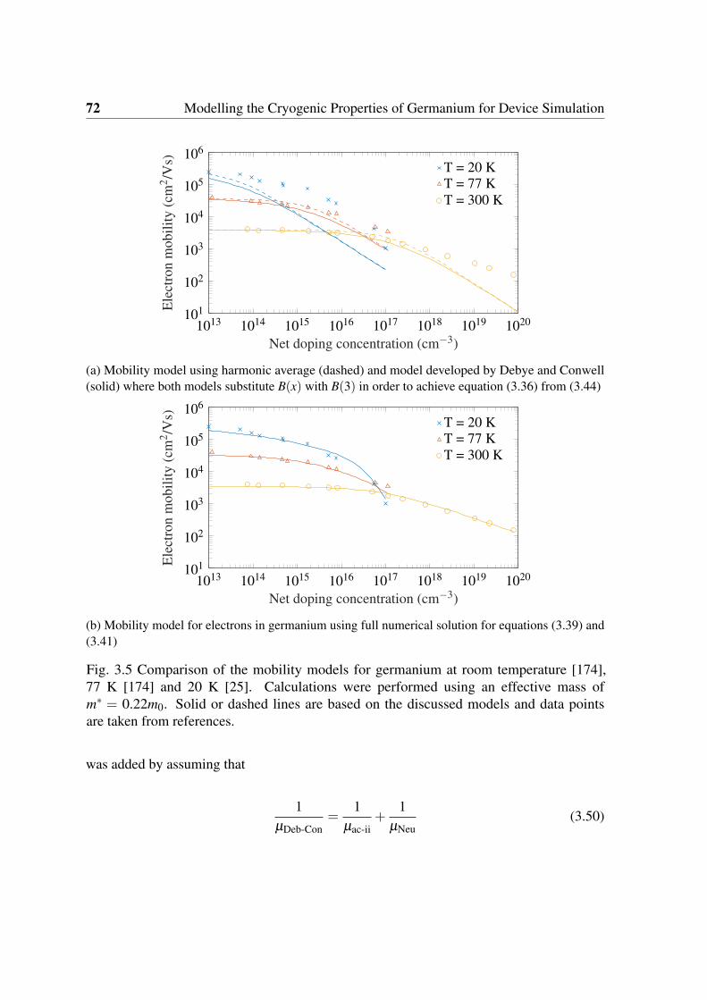
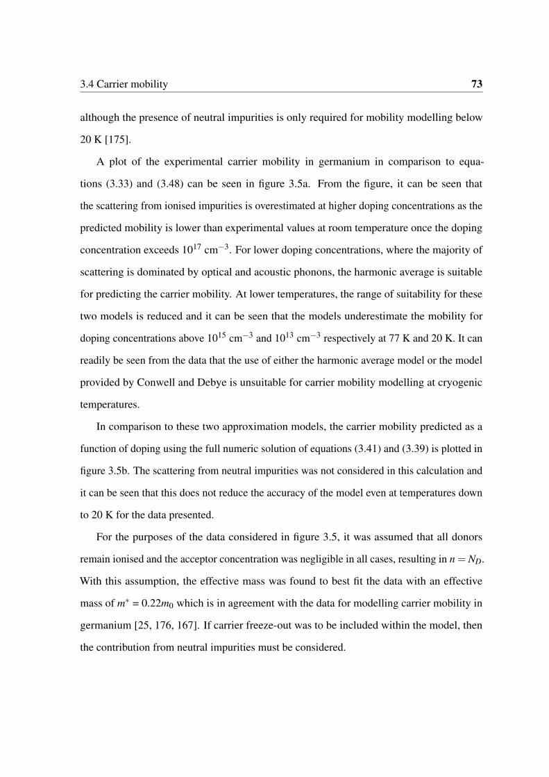
Transcript
Modelling the Cryogenic Properties of
Germanium for Emerging Liquid
Hydrogen Power Applications
Luke Bradley
Supervisor: Dr. Angela Dyson
Advisor: Dr. Glynn Atkinson
School of Engineering
Newcastle University
This dissertation is submitted for the degree of
Doctor of Philosophy
May 2020
Acknowledgements
Firstly, I would like to thank my family and all my friends for the work completed whom
I could not have completed this work without. During all the hard times, I have always
received great support from all these people who have encouraged me through every stage of
this process.
I must also give thanks to the Engineering and Physical Sciences Research Council for
providing with this grant to conduct and complete this research. As well as this, I would like
to thank Andrea Dawson and Thomas Coulson for allowing me to use the equipment and
facilities within the Physics department and Newcastle University to measure my devices.
For the measurements of my ZrO2/Ge MOS capacitors, I must also thank Andrew Stokes
of the INEX company within Newcastle for his advice on MOS capacitor fabrication and
wire bonding expertise without which I would not be able to have measured my devices
within cryogenic environments.
I would also like to personally thank my supervisors Angela Dyson, Glynn Atkinson and
Alton Horsfall for all of their contributions, advice and direction towards the completion of
this work. As well as these people, I would like to thank Anthony O’Neill, Nick Wright,
Jonathon Goss, Dan Naylor and all others academics within the research group here at
Newcastle university for their advise and expertise.
Abstract
In recent years, there has been an increase in research focused towards the reduction and/or
elimination of greenhouse emissions from applications used in everyday life. In addressing
this, liquid hydrogen has been highlighted as an attractive alternative fuel source for commer-
cial vehicles due to it’s lower weight, higher power density and zero greenhouse emissions in
comparison to petrol and diesel fuels. Incorporating such a fuel source however introduces
a cryogenic environment of 20 K affecting the power electronics used to deliver the power
from source to load.
Herein, the physical properties of semiconductors influencing the overall efficiency of
devices within an H-bridge circuit are considered. From this, germanium is hypothesised to
be the most suitable semiconductor for power devices at or near temperatures of 20 K.
Closed-loop models are developed for the carrier concentration, carrier mobility, carrier
velocity, for both electrons and holes as a function of doping concentration and temperature
with critical analysis of the range of suitability for each. Multiple models are also developed
for both carrier concentration and carrier mobility which offer a trade off depending on
whether one requires accuracy or simplicity in calculation.
A significant influence on the device characteristics of MOSFETs is that of the oxide/sem-
iconductor interface. For the first time, ZrO2 is fabricated directly on germanium substrates
through the thermal oxidation of zirconium on germanium. The interface state density of
these capacitors are comparable to literature values offering a much cheaper and simpler
fabrication method for high-κ dielectric formation on germanium substrates. The leakage
vi
current density of the ZrO2 MOS capacitors are low in comparison to reported values and
are shown to decrease with decreasing temperature.
With the physical models of both bulk and interfacial germanium, multiple PiN germa-
nium diodes are simulated using technology computer aided design (TCAD) that show the
potential for germanium power devices with breakdown voltages in excess of 800 V at room
temperature and 400 V at 20 K. Simulations of vertical power MOSFETs incorporating
a ZrO2 interlayer show great promise for low temperature power electronics at or near
20 K where other commercial devices experience significant resistive losses. With the work
conducted here, vertical power MOSFETs fabricated using germanium and ZrO2 open the
gateway for low voltage applications incorporating liquid hydrogen fuel cells.
Table of contents
List of figures x
List of tables xvii
Nomenclature xviii
1 Introduction 1
1.1 Motivation: Highly efficient commercial vehicles with a H2 based fuel source 2
suitable semiconducting materials for cryogenic power electronics, The Journal of
Engineering, 2019(17):4475-4479, Jun 2019.
1.3 Key contributions 7
As well as this, at least two papers are expected to be submitted based on the modelling
work conducted in chapter 3 and experimental data in chapter 4. The modelling work in
chapter 3 highlights the importance of using the correct mobility and ionisation model
at low temperatures in order to accurately recreate experimental data for germanium at
low temperatures, whilst the experimental data from chapter 4 explores the temperature
dependence of leakage currents within ZrO2 on germanium in addition to the development
of a model that predicts the leakage current as a function of temperature, voltage and oxide
thickness.
Chapter 2
Literature Review: Properties of
cryogenic power electronics and
semiconductors at cryogenic
temperatures
2.1 Introduction
The area of electronics for high power applications has received a lot of attention in recent
years as one of the major limiting factors of the overall efficiency in motor and generator
systems is limited by the maximum switching frequency and resistive losses of the control
electronics. Maintaining a lower operating temperature using proper thermal management
reduces the overall resistive losses of power devices whilst choosing a highly conductive
semiconducting material for device fabrication will also serve to reduce the on-state losses.
This chapter aims to address the requirement for semiconducting transistor switches and
10Literature Review: Properties of cryogenic power electronics and semiconductors at
cryogenic temperatures
diodes in high power switching circuits with focus towards motor applications incorporating
liquid hydrogen fuel cells.
2.2 Power electronics in DC control circuits
In drive applications, motors can be powered using an AC or DC power source. Both types of
machines offer disadvantages and advantages in comparison to the other and manufacturers
often prioritise one depending on the application. In terms of control, DC machines are far
more favourable than AC motors as they have a higher speed, greater ease of control and
low starting torque compared to AC motors. As such, DC motors are typically used for
low voltage motors that require quick response time and precise control that is more easily
achieved in comparison to AC motors [30–32].
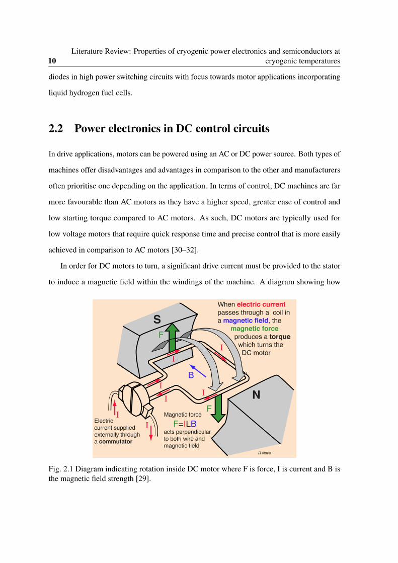
In order for DC motors to turn, a significant drive current must be provided to the stator
to induce a magnetic field within the windings of the machine. A diagram showing how
Fig. 2.1 Diagram indicating rotation inside DC motor where F is force, I is current and B isthe magnetic field strength [29].
2.2 Power electronics in DC control circuits 11
rotation is achieved in a DC machine can be seen in figure 2.1. A rotor is placed between two
stationary magnets providing a continuous magnetic field. If a DC current is passed through
the rotor, the rotor will experience a force given by
Force = BIL (2.1)
where B is the magnetic field strength, I is the current and L is the distance between the
rotor and magnet resulting in rotation. By increasing the current, the force acting on the wire
can be increased, although the rotation of the motor can only be reversed by reversing the
direction of the current. In order to allow for directional and speed control of the motor, a
switching circuit must be employed to control the direction of current through the motor.
A commonly used method by which to control the direction and speed of a DC motor
is to use an H-bridge circuit [33, 34] in which a DC motor is placed at the centre of 4 high
power switches as shown in figure 2.2. When switches F1 and F2 are pressed, current can
flow from left to right through the motor leading to rotation, similarly, by pressing switches
B1 and B2, the direction of the current can be reversed. By replacing the switches with
transistors and a subsequent transistor switching circuit, the direction and speed of the motor
can be controlled.
M
F1
F2
B1
B2 Vsup
(a) H-bridge diagram using 4 push to makeswitches and DC motor
M
F1
F2
B1
B2 Vsup
(b) Motor rotates forward when switches F1 andF2 are pressed
Fig. 2.2 H-bridge using push to make switches and a DC motor.
12Literature Review: Properties of cryogenic power electronics and semiconductors at
cryogenic temperatures
2.2.1 MOSFETs as a switch for current control
A transistor is used as a switch within an electronic circuit to control the flow of current
through the application of a voltage on a gate contact. A diagram of a lateral and vertical
MOSFET can be seen in figure 2.3 along with an example of the switching characteristics of
a commercial 25 V n-type silicon MOSFET [35] and a commercial high power 1.2 kV SiC
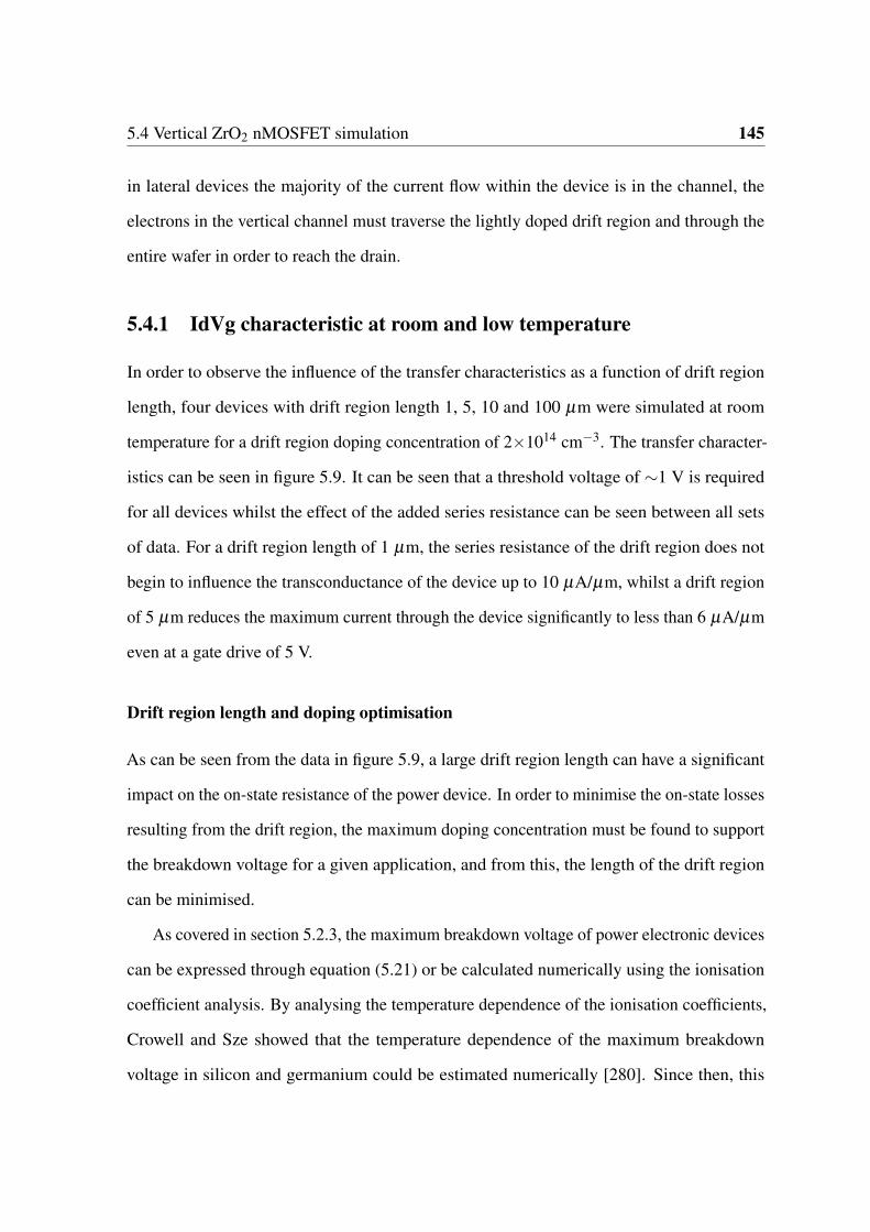
MOSFET [36].
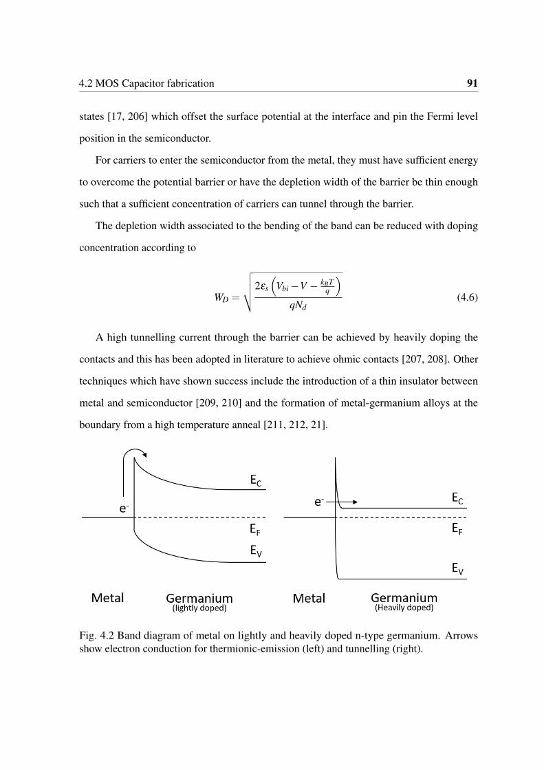
For both MOSFETs, electron conduction cannot occur from source to drain unless a
sufficient gate voltage has been achieved. By applying a positive gate bias, minority electrons
within the p-type region of both devices are attracted to the oxide/semiconductor interface
of the device. Once the gate voltage has exceeded the threshold voltage of the device, the
concentration of electrons near the interface will exceed the majority hole concentration
forming an n-type region at the interface. With this n-type region near the interface, electrons
are able to conduct from source to drain. The threshold voltage itself has two common
definitions which include the voltage at which the drain current achieves a certain level or by
taking the voltage intercept of the tangent at the maximum gradient from a drain current-gate
voltage (IDVG) profile.
The transfer characteristics of a low and a high power MOSFET can be seen in figures 2.3c
and 2.3e. As can be seen for both devices, beyond a certain threshold voltage, the drain
current increases exponentially. At higher temperatures, the threshold voltage of both devices
decreases. For the power device, it can be seen that at high gate voltages, the gradient begins
to decrease which is due to an increase in the resistance of the lightly doped drift region of
the device [37, 38].
As shown in figures 2.3d and 2.3f, following the application of a gate bias exceeding the
threshold voltage, the drain current can be increased linearly with drain to source voltage. As
the drain voltage increases, the difference in the gate voltage with respect to the substrate
decreases and the concentration of carriers near the drain end begins to decrease. At this point,
2.2 Power electronics in DC control circuits 13
N+
P-
Drain Source Gate
Substrate
e-
(a) Lateral n-type MOSFET
P+ P+
N-
N++ N++
N+
Source Source Gate
Drain
e- e-
(b) Vertical n-type MOSFET
(c) IdVg of commerical FDV303N MOSFET (d) IdVd of commerical FDV303N MOSFET
(e) IdVg of commerical SCT50N120 MOSFET (f) IdVd of commerical SCT50N120 MOSFET
Fig. 2.3 Structure of standard n-type lateral (a) and vertical power MOSFET (b) where arrowsindicate direction of electron flow. Transfer and output characteristics of low power MOSFET(c,d) and vertical power MOSFET (e,f) are taken from commercial data sheets [35, 36].
14Literature Review: Properties of cryogenic power electronics and semiconductors at
cryogenic temperatures
the drain current becomes sub-linear before eventually saturating to a drain independent
value know as the saturation current. Once the drain current has saturated it can only be
increased by increasing the gate voltage.
By including a large lightly doped drift region, the vertical power MOSFET is capable of
supporting blocking voltages in excess of 1 kV [39, 40] but also results in larger threshold
voltages and saturation voltages. Despite this, high power transistors are commonly used in
high voltage motor applications for both DC and AC applications [41–43].
2.2.2 Power MOSFETs and Diodes in H-bridge circuits
An example of a switching circuit incorporating 4 n-type MOSFETs can be seen in figure 2.4.
Similarly to the circuit in figure 2.2, by switching transistors F1 and F2, a current will
flow through the motor from left to right driving the motor and the direction of the current
can be switched by turning off transistors F1 and F2 and switching on B1 and B2. The
switching of the transistors within the H-bridge circuit is performed through a control gate
drive microprocessor that controls the signals sent to the gate contacts of each transistor. An
example of the gate drive switching characteristics can be seen in figure 2.5.
For a duty cycle of 50%, both sets of transistors are switched on and off for the same
period of time and the average current through the motor is zero. For a duty cycle above
or below 50%, the average current through the motor will either flow in one direction or
the other and the speed of the motor can be controlled by defining the duty ratio of each
MOSFET.
As can be seen from the switching characteristics, there exists a short period of time
where switching of the current and voltage from on to off or off to on results in a significant
increase in power loss. As well as these losses, on-state and off-state losses are also present
due to the ohmic losses of the transistor in steady-state conditions. As will be shown later,
2.2 Power electronics in DC control circuits 15
these losses can be minimised by choosing a device with a low on-state resistance, low
switching time and low parasitic capacitances.
Free-wheeling diode
Within the H-bridge circuit, 4 diodes are connected in reverse bias with the drain and source
of each MOSFET. The purposes of these diodes are to protect each MOSFET from voltage
breakdown resulting from current switching. Considering a circuit with parasitic inductances,
or solely considering the motor which acts as an inductor and resistor in series within a
M
F1
F2
B1
B2 Vsup
(a) H-bridge circuit for DC motor (b) Parasitic components of n-typeMOSFET
(c) Wave forms acting on the gate of MOSFETs F1,2 and B1,2. Different timing ratios for the MOSFETpairs allows for control of the current density through the motor.
Fig. 2.4 Circuit diagram of H-bridge circuit including pin out diagram of n-type MOSFETwith parasitic capacitances. Duty cycle of 50% is achieved when both t1 and t2 are equal,altering this ratio results in a driving current and rotation of motor.
16Literature Review: Properties of cryogenic power electronics and semiconductors at
cryogenic temperatures
circuit, the voltage induced from an inductor is given by
V (t) = L∂ i∂ t
(2.2)
where L is the inductance of either the motor or the parasitic components within the circuit
and t is time. As the transistor switches from positive to negative current, the voltage induced
over the drain and source of the motor will induce a large voltage in the reverse direction as
charge is built up on the source contact of the MOSFET. In order to eliminate this charge, the
freewheeling diode creates a loop of current through the source and drain of the MOSFET
and the charge is dissipated through resistive losses.
As well as the resistive losses, extra losses in the diode can come from the reverse
switching, that is, when the transistor is switched on, the diode becomes subjected to a
sudden large reverse bias. As can be seen in figure 2.5, the switching of a diode from forward
current to reverse current results in a large reverse current. At t1, the current through the diode
is switched from positive to negative. For a small period of time, the current through the
diode in reverse direction can achieve current levels within the same order of magnitude as
the current levels of the forward direction as there is a concentration of charge stored within
the diode from the forward conduction. At time t2, the voltage of the diode approaches zero
Ploss
t
Vds
Ids
Ioff
Ion
Von
Voff
toff ton
t
Idiode
Vdiode
t1 t2 t3
Fig. 2.5 Voltage and current switching characteristics of MOSFET and diode in H-bridgecircuit. Ringing due to parasitics not included.
2.2 Power electronics in DC control circuits 17
and the current in the reverse direction reaches the peak reverse current. At this point, the
current begins to decay to the leakage current value whilst the voltage decays to the reverse
of the bias applied to MOSFET drain to source. The losses incurred from the switching are
dependent on the maximum recovery current and reverse recovery time equal to t3 - t1 and
can be reduced by selecting a diode with a high carrier mobility and high carrier lifetime [44].
2.2.3 Power loss
Due to the high current densities and large supply voltages, power electronic devices ex-
perience significant power loss and must be thermally managed in order to remain within
specific operating temperatures. An example of a heat map of a SiC MOSFET and a silicon
isolated gate bipolar transistor (IGBT) can be seen in figure 2.6. As can be seen, during
device operation, the temperature of both devices has risen to over 120 °C and is common
for high-temperature power devices fabricated from silicon, SiC and GaN [45–47].
The resistive power loss of an electronic device with a time unvarying on-state current
Ion is given by
Pcond = I2onR (2.3)
(a) Infared image of SiC module (b) Junction temperature vs time
Fig. 2.6 Infared heat map of 1.7 kV, 450 A SiC module and junction temperature of devicecompared to a high power silicon IGBT [48].
18Literature Review: Properties of cryogenic power electronics and semiconductors at
cryogenic temperatures
where R is the device resistance. The switching loss of a transistor switch is given by
Pswitch = 0.5I2onR fsw(ton + to f f ) (2.4)
where fsw is the switching frequency, and ton and to f f are the on and off switching times
given by
ton = tri + t f v (2.5a)
to f f = t f i + trv (2.5b)
where, respectively, tri and t f v are the rise time of the current and fall time of the voltage
and t f i and trv are the fall time of the current and rise time of the voltage. The total loss of a
transistor in a switching circuit is finally
PTotal = PcondD+Pswitch (2.6)
where D is the duty cycle equal to ton/to f f . By considering the individual power loss
components, it can be seen that the power loss can be minimised through minimising the
series resistance.
In reducing switching losses, it has been found that the total rise time and fall time of the
transistor increases with the parasitic capacitances of the device. As charge is stored at the
gate and drain with respect to the ground potential at the source, parasitic capacitances will
exist between the three terminals as illustrated in figure 2.4b.
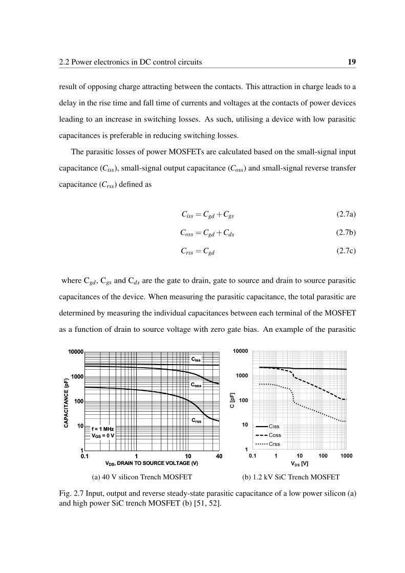
Parasitic capacitance components
The influence of the parasitic capacitances on the total rise time and fall time of the devices has
been shown to be directly correlated to the switching losses in power MOSFETs [49, 50, 11].
The parasitic capacitances of a device are present between the contacts of a device and are the
2.2 Power electronics in DC control circuits 19
result of opposing charge attracting between the contacts. This attraction in charge leads to a
delay in the rise time and fall time of currents and voltages at the contacts of power devices
leading to an increase in switching losses. As such, utilising a device with low parasitic
capacitances is preferable in reducing switching losses.
The parasitic losses of power MOSFETs are calculated based on the small-signal input
capacitance (Ciss), small-signal output capacitance (Coss) and small-signal reverse transfer
capacitance (Crss) defined as
Ciss =Cgd +Cgs (2.7a)
Coss =Cgd +Cds (2.7b)
Crss =Cgd (2.7c)
where Cgd , Cgs and Cds are the gate to drain, gate to source and drain to source parasitic
capacitances of the device. When measuring the parasitic capacitance, the total parasitic are
determined by measuring the individual capacitances between each terminal of the MOSFET
as a function of drain to source voltage with zero gate bias. An example of the parasitic
(a) 40 V silicon Trench MOSFET (b) 1.2 kV SiC Trench MOSFET
Fig. 2.7 Input, output and reverse steady-state parasitic capacitance of a low power silicon (a)and high power SiC trench MOSFET (b) [51, 52].
20Literature Review: Properties of cryogenic power electronics and semiconductors at
cryogenic temperatures
components measured for a silicon and SiC power Trench MOSFETs can be seen in figure 2.7.
As can be seen, as the drain to source voltage increases, the output and reverse steady-state
capacitance decreases monotonically. The cause of this is due to an increase in device leakage
resulting in a reduction in accumulated charge at the drain contact. For the input steady-state
capacitance, it can be seen that for both devices, it remains essentially voltage independent
whilst also remaining the largest parasitic component of both devices.
The reason for the high input steady-state capacitance in comparison to the output and
reverse steady-state is due to the close proximity of the gate and source contacts. For two
parallel plates, the capacitance generating between the two plates is given by
C =ε0εrA
d(2.8)
where ε0 and εr are the dielectric constant of the vacuum and the relative dielectric constant
of the medium, A is the area and d is the distance between the two plates. For air, εr is unity
whilst it takes a value of 11.7 in silicon. Although the geometry of the contacts of the trench
MOSFETs is not that of two parallel plates, the capacitance between the contacts will be
greater for contacts that are within close proximity of one another in comparison to contacts
that are far apart. As such, the Ciss, which is the only component that relies on the Cds will
be much greater than that of Coss and Crss.
For diodes, the reverse polarity of the diode when placed in parallel with any power MOS-
FET results in a large capacitance that contributes to an increase in the off-state switching
of the MOSFET but does not affect the on-state switching. Typically, the capacitance of
power diodes varies in a similar manner to that of Coss and Crss of the power MOSFET with
a significant contribution resulting from the length of the drift region. By incorporating a
device with a large drift region, a large blocking voltage and low capacitance can be achieved;
although this does result in an increased on-state resistance.
2.3 Performance of Power Electronic Devices at Cryogenic Temperatures 21
By minimising the parasitic capacitances of the power devices, the on and off times of
the MOSFETs will reduce; resulting in lower switching losses. As well as this, the switching
loss can be further minimised by selecting a material with a high carrier mobility as it will
take less time for charge to enter/leave the device during a switching cycle.
2.3 Performance of Power Electronic Devices at Cryogenic
Temperatures
With the recent development and incorporation of liquid hydrogen fuel cells in automotive
vehicles, the suitability of commonly used devices and commercial power electronics has
recently received a lot of attention for extreme environments [55, 56, 54, 57–59].
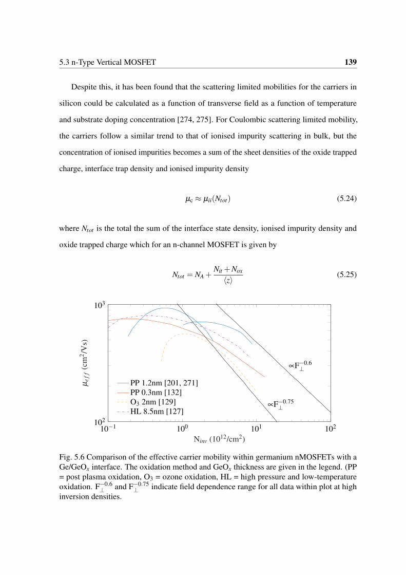
A plot of the on-state resistance for a SiC and GaN power MOSFETs can be seen
in figure 2.8. For GaN (and also silicon) devices, the on-state resistance and thermal
management of devices decreases with a reduction in temperature due to an increase in
carrier mobility and thermal conductivity. For SiC devices, due to the greater breakdown
field in comparison to silicon, power devices with breakdown voltages in the kV range can be
(a) 200 V GaN MOSFET from Efficient Power Conversion(EPC)
(b) 5 1.2 kV SiC MOSFETs from differentmanufacturers
Fig. 2.8 Temperature dependence of the on-state resistance of a high power 200 V GaN (a)and 5 different 1.2 kV SiC MOSFETs (b) [53, 54].
22Literature Review: Properties of cryogenic power electronics and semiconductors at
cryogenic temperatures
fabricated with drift region doping concentrations exceeding 1015, although this high doping
concentration results in a negative temperature coefficient for the on-state resistance as the
increased scattering from dopants reduces the carrier mobility with reducing temperature.
As a result of the different temperature coefficients for the resistance of the SiC and GaN,
GaN is proposed as a more suitable material for low-temperature electronics in comparison
to SiC which is primarily considered for high-temperature applications.
For the majority of commercial MOSFETs, an increase in the threshold voltage of the
device is experienced with a reduction in temperature. The temperature characteristics of
the measured threshold voltage within selected GaN, SiC, and silicon devices can be seen
in figure 2.9. The increase in threshold voltage is attributed to the reduction in minority
carrier concentration within the p-region of enhancement mode devices. For GaN devices,
this increase in threshold voltage is typically negligible, but for the silicon and SiC devices,
the threshold voltage increases by more than 2 and 3 times respectively. Whilst this could be
a problem for complimentary-MOS applications which aim to use lower driving voltages,
the gate driving voltage used in the on-state regime of power electronic devices is typically
of the order of 10-15 V and so this difference in threshold voltage can be neglected.
(a) 200 V GaN MOSFET from Efficient Power Conver-sion (EPC)
(b) Threshold voltage of two 1.2 kV SiCMOSFETs and a 1.2 kV silicon IGBT
Fig. 2.9 Measured threshold voltage in a 200 V GaN (a) and SiC and Si power FETs(b) [53, 60].
2.3 Performance of Power Electronic Devices at Cryogenic Temperatures 23
Device switching
In measuring the switching characteristics, it has been found that the losses reduce with
reducing temperature for silicon and GaN devices whilst they increase for SiC [62, 60, 63].
Whilst the capacitance at high drain biases remains essentially temperature independent [58],
the reduction in device switching comes from the reduced switching times due to a lower
series resistance resulting in faster charging/discharging.
As a result of this, it has been found that for the majority of power electronic circuits, SiC
MOSFETs are commonly deemed less suitable as the increase in switching losses and on-
state losses results in a lower circuit efficiency whilst GaN and silicon increase in efficiency
with reduction in temperature down to 77 K.
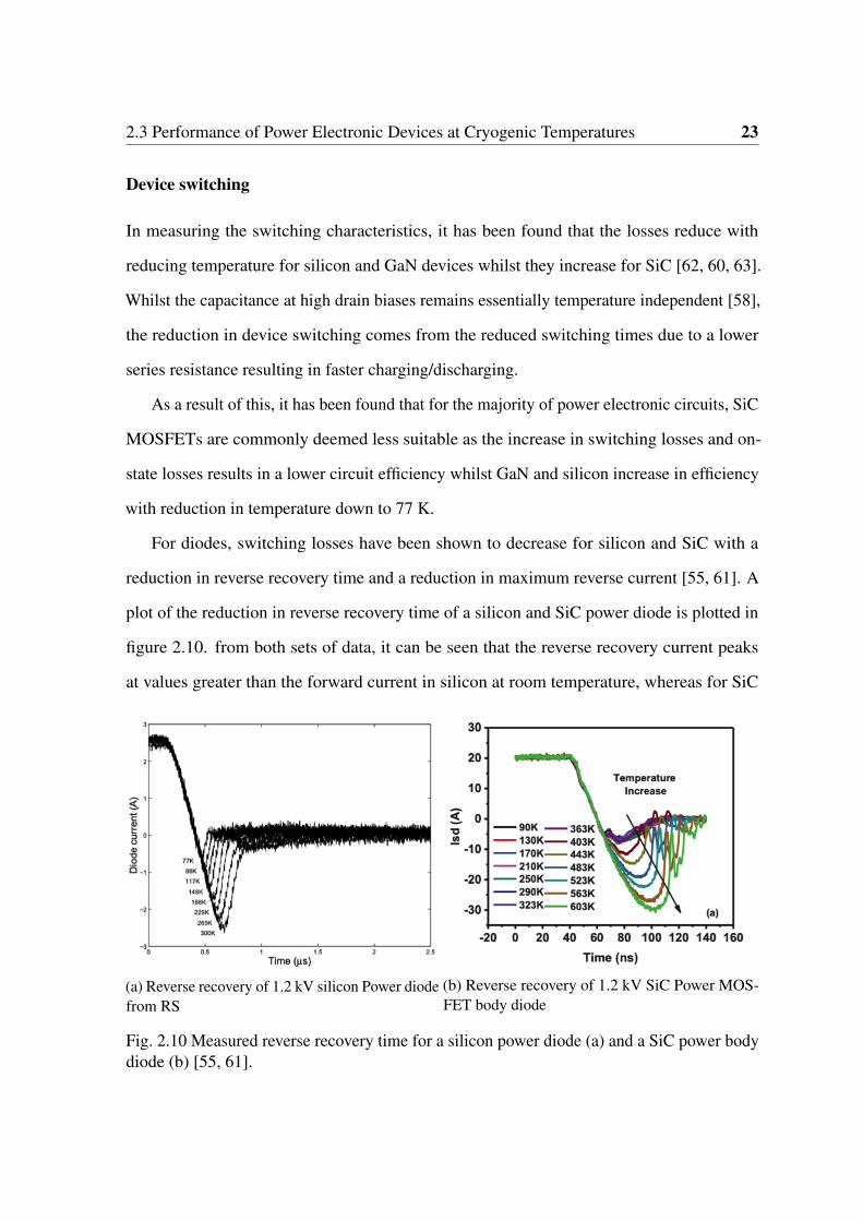
For diodes, switching losses have been shown to decrease for silicon and SiC with a
reduction in reverse recovery time and a reduction in maximum reverse current [55, 61]. A
plot of the reduction in reverse recovery time of a silicon and SiC power diode is plotted in
figure 2.10. from both sets of data, it can be seen that the reverse recovery current peaks
at values greater than the forward current in silicon at room temperature, whereas for SiC
(a) Reverse recovery of 1.2 kV silicon Power diodefrom RS
(b) Reverse recovery of 1.2 kV SiC Power MOS-FET body diode
Fig. 2.10 Measured reverse recovery time for a silicon power diode (a) and a SiC power bodydiode (b) [55, 61].
24Literature Review: Properties of cryogenic power electronics and semiconductors at
cryogenic temperatures
this only occurs when the temperature exceeds 450 K. For GaN devices, there is a negligible
change in the reverse recovery characteristics of measured high power diodes [64], with
quicker recovery rates than silicon although slower when compared to SiC [65–67].
Breakdown voltage
The breakdown voltage of power devices is dependent on the ionisation coefficients for
electrons and holes and the distribution of the electric field within the device [70–72]. It has
been shown that for low and high power devices, the ionisation factors for electrons and
holes gradually increases with reducing temperature. A plot of the measured breakdown
voltage for a silicon and SiC power MOSFET can be seen in figure 2.11. As can be seen
for the silicon device, the breakdown voltage decreases gradually to approximately 80 %
of the room temperature value. For the SiC device, the breakdown voltage can be seen to
reduce gradually from 1700 to 1600 V from room temperature to 150 K for both devices.
Below 150 K, the breakdown voltage reduces significantly in device (b) to 1325 V at 77 K
whilst device (a) only reduces to 1550 V. The difference in breakdown voltage trend at low
temperatures was not investigated further and was determined to be related to packaging
(a) silicon 650 V power MOSFET (b) 4H-SiC 1200V power MOSFET
Fig. 2.11 Temperature dependence of the breakdown voltage within high power silicon (a)and SiC (b) power MOSFETs [68, 69].
2.3 Performance of Power Electronic Devices at Cryogenic Temperatures 25
issues [68]. The gradual reduction in breakdown voltage with reducing temperature must be
taken into consideration when designing a power device for low-temperature applications.
2.3.1 Operation of vertical power MOSFETs
As the name implies, a vertical MOSFET is simply a linear MOSFET that has been fabricated
such that the conduction of carriers is vertical rather than lateral. By doing so, it is possible
for manufactures to add a thick lightly doped drift region that is essential to ensure a large
breakdown voltage for power electronic devices. The two common device structures for
vertical power MOSFETs are the double-diffused and trench MOSFETs both of which can
be seen in figure 2.12.
Similar to the operation of the lateral MOSFET, the total current through a vertical
MOSFET is limited by the gate bias and the total resistance of each region. Considering an
n-type double-diffused MOSFET, conduction of electrons from source to drain cannot occur
as there is a p-type region blocking conduction from the n+ region near the source and the
n− body. In order for a current to flow, an n-type inversion channel must be created at the
oxide/p-type region interface through the application of a positive gate bias. The bias required
to create a sufficient channel for conduction is known as the threshold voltage which typically
ranges from 1-3 V depending on the operating temperature, channel doping concentration
and oxide capacitance. Once a sufficient gate bias has been achieved, electrons can conduct
from source to drain. Initially, the current increases linearly with drain to source voltage.
As the drain to source voltage increases, the relative difference in the gate voltage and the
voltage at the oxide/p-type region near the drain decreases leading to a gradual reduction in
current until eventually the current saturates to a voltage independent value.
The functionality of the trench MOSFET (or sometimes referred to as the UMOS) is
equivalent to that of the double-diffused MOSFET. The key difference between the two
FET designs are the direction of the current conduction in the channel and the total on-state
26Literature Review: Properties of cryogenic power electronics and semiconductors at
cryogenic temperatures
resistance. When considering the conduction path of electrons in double-diffused MOSFETs,
it can be seen that carriers are confined between two PN regions once they pass through the
channel. These carriers are scattered due to the close proximity of the current path to the
Fig. 2.12 Structure and electron conduction path in n-type double-diffused MOSFET (a) andtench MOSFET (b).
2.3 Performance of Power Electronic Devices at Cryogenic Temperatures 27
bias generated at the p-type/n-type regions reducing the total effective current area in the
body. This effect is known as the parasitic JFET resistance that is observed in both n-type
and p-type double-diffused MOSFETs but is not observed in trench MOSFETs due to the
removal of carrier conduction in-between two diffused p-type regions.
Despite the reduced on-state resistance, trench MOSFETs are harder to fabricate due to
the optimisation of the oxide trench depth and semiconductor side wall oxidation and, as
such, both transistor types can be found commercially and in literature. Here, we will be
considering the on-state resistance of vertical n-type trench MOSFETs as we are aiming to
determine the minimum achievable on-state resistance for power electronic devices fabricated
from germanium.
2.3.2 Alternative high power transistors
As well as high power MOSFETs, other transistor structures include bipolar junction tran-
sistors (BJTs), IGBTs and high electron mobility transistors (HEMTs) and are shown in
figure 2.13. In the on-state, the transfer characteristics of each of these transistors is similar
to that of a power MOSFET but fundamentally works on a different current conduction
mechanism for each device.
For BJTs, the total emitter current is a sum of the collector current (IC) and base current
(IB)
IE = IC + IB = β IB + IB (2.9)
where β is the DC current gain. The DC current gain of the bipolar transistor is based on the
minority carrier diffusion current from emitter to drain which increases due to the injection
of carriers at the base resulting in a magnification of the collector current. As a result of
the current magnification, the on-state resistance of power BJTs are low in comparison to
power MOSFETs but suffer in switching losses due to the long transport times of minority
carriers within the device as well as requiring both electron and holes to traverse the length
28Literature Review: Properties of cryogenic power electronics and semiconductors at
cryogenic temperatures
P+
N-
N++ N++
N+
Emitter Emitter Base
Collector
e- e-
h+
P+ P+
N-
N++ N++
P+
Emitter Emitter Gate
Collector
e- e- h+ h+
n-AlGaN
Bulk GaN or sapphire
Drain Source Gate
Substrate
i-GaN e-
Fig. 2.13 Typical power transistor structure for a BJT (top), IGBT (middle) and HEMT(bottom) where arrows indicate electron and hole conduction.
2.3 Performance of Power Electronic Devices at Cryogenic Temperatures 29
of the device. As well is this, measurements at cryogenic temperatures show a significant
reduction by nearly two orders of magnitude for the current gain at 77 K in comparison to
room temperature and an increase in switching time [73–75].
The IGBT merges the current gain of the BJT with the gate control of the MOSFET and
is often used for high current medium voltage applications. The current conduction of the
IGBT is highlighted in figure 2.13. For an n-type IGBT, the hole conduction is based on
the characteristics of a PNP bipolar transistor whilst the electron conduction is based on the
MOSFET conduction through the gate and must also diffuse through the P+ layer. Down to
77 K, the on-state and switching losses reduce compared to the room temperature value but
increase for the majority of commercial devices at temperature below 77 K [60, 76].
Finally, the recent advances in GaN fabrication has lead to the commercialisation of
lateral high power HEMTs with breakdown voltages in excess of 600 V [38]. At the interface,
a 2-dimensional electron gas (2DEG) is formed through the polarisation of carriers generated
from surface states into the channel. Due to the high carrier concentration, the carriers are
effectively screened from impurities within the AlGaN layer which, when coupled with the
low doping concentration of the GaN layer, results in a much greater carrier mobility in
comparison to bulk GaN [77]. As a result of the high electron mobility, GaN devices have
much faster switching times and higher conductivity’s than the majority of commercial power
devices in the same voltage range but suffer from quick degradation [78, 79].
Comparative studies [80–82, 37] on the performance of power transistors at cryogenic
temperatures have shown that for temperatures below 20 K, unipolar and HEMT devices
exhibit the greatest reduction in on-state resistance and switching losses of all fabricated
devices. A more physical insight into the temperature dependence of the on-state and
switching losses of power electronic devices shows that the main contribution to a low
resistance device is a high carrier mobility and high carrier concentration which is dependant
on both device structure and semiconducting material.
30Literature Review: Properties of cryogenic power electronics and semiconductors at
cryogenic temperatures
2.4 Determination of optimal material for cryogenic appli-
cations
The choice of semiconducting material for power devices depends largely on the application
of use. For low power applications, such as logic devices, manufacturers are primarily
focused towards the maximum operating frequency of a device which is dependant on
the speed of charge transfer through a material. For high power applications, such as the
control of driving current through an electrical actuator, the conductivity and power transfer
characteristics are the key parameters which determine the suitability of a material for devices.
Regardless of the application, the key figures of merit for each material are dependant on
their physical properties and must be considered for all applications.
In cryogenic environments, the physical properties of semiconducting materials vary
greatly from their room temperature values and is the cause of the difference in temperature
dependence of the on-state resistance of SiC, GaN, and silicon power devices [80, 72, 83].
By taking into consideration the material dependant mechanisms that lead to an improvement
of power electronic devices with reducing temperature, the optimal material for high power
devices can be determined. In this chapter, commercially available semiconducting Si, Ge,
GaAs, 4H-SiC and GaN devices are compared in order to identify the optimal semiconducting
material for cryogenic power electronic applications.
2.4.1 The Requirement for highly efficient power electronics at temper-
atures below 77 K
A number of applications are examining the possibility of using superconducting cables
for the transfer of electrical power, in an effort to increase the efficiency of circuits used to
deliver power from source to load [84]. This is being driven by on-going research to identify
more efficient designs for air travel, which are being pursued by organisations including
2.4 Determination of optimal material for cryogenic applications 31
NASA and ATI [85, 10, 86]. In the last decade, NASA has proposed a hybrid-electric
propulsion system, that in conjunction with a new aircraft design, is estimated to be around
70% more efficient than the conventional airliners that are in use today [87] that is based
on the combustion of liquid hydrogen as a fuel source. As well as this, recently emerging
applications are looking at incorporating liquid hydrogen fuel cells for low voltage DC
motors [3] and standalone wind-hydrogen plants [2]. In order to provide control over the
behaviour of the machine and provide isolation in the case of failure, a control circuit will
be required that comprises of power electronics devices that can operate when cooled by
liquid hydrogen. In an attempt to maximise the efficiency of these cryogenic power systems,
the power distribution network will incorporate superconducting cables that will eliminate
resistive losses [88]. The boiling point of liquid hydrogen is 20.28 K and this enables both
the machine and the power distribution system to be fabricated using magnesium diboride,
MgB2 which has a superconducting transition temperature of 40 K [12].
Because of the high currents within a superconducting system, the on-state resistance
of a power electronic circuit will be the most significant source of inefficiency in a cryo-
genic circuit. In order for a power electronic MOSFET to be suitable for liquid hydrogen
applications, it must demonstrate a:
1. Reduced on-state resistance at 20 K in comparison to 300 K
2. Fast switching speeds with low parasitic capacitances
3. High thermal conductivity for good thermal management
In order to determine the ideal semiconducting material to reach these requirements, the
temperature dependence of the physical properties of each material must be considered.
32Literature Review: Properties of cryogenic power electronics and semiconductors at
cryogenic temperatures
2.5 Temperature Dependence of Bulk Semiconducting Prop-
erties
The choice of semiconductor for the realisation of power electronics circuits is dependent on
the range of operating temperatures the circuit will encounter. For high-temperature applica-
tions (T> 400 K), the superlative material properties and silicon like process technologies of
the numerous polytypes of SiC have resulted in them becoming the material of choice for
power electronic devices. At intermediate temperatures (123 K<T< 400 K), the significant
knowledge of Si characteristics, coupled with the financial benefits of using such an abun-
dant material has lead to it being the most technologically advanced and commonly used
semiconductor, despite the presence of materials that offer more beneficial characteristics.
2.5.1 Carrier mobility as a function of temperature and doping
When considering the maximum device switching speed, the mobility and length of the
device are the key figures of merit. During the charging/discharging of a device contact such
as the drain, the rise time and fall time of the current is dependent on the capacitance and
resistance of the device. For example, the switching and on-state losses of power MOSFETs
have been shown to be directly proportional to the series resistance of the device [89, 90]
which can be minimised through maximising the carrier mobility.
As the operating temperature is reduced, the physical properties of a semiconductor
change, resulting in a change in how electronic devices fabricated from these semiconductors
behave. For example, a comparison of the electron and hole mobilities in Ge, Si, 4H-SiC
and GaAs as a function of temperature for low and intermediate doping concentrations is
shown in figure 2.14. From the data, it can be seen that as the temperature reduces, the carrier
mobility within all semiconductors increases although the rate of change with temperature is
different for all materials.
2.5 Temperature Dependence of Bulk Semiconducting Properties 33
For low doping concentrations where the net doping concentration is of the order of
1014 cm−3, the mobility at intermediate to high temperatures is limited by the scattering from
optical and acoustic phonons. Theoretically, the lattice scattering limited mobility resulting
from acoustic phonons is expected to follow a T−1.5 temperature dependence [26], although
the combination of acoustic and optical phonon scattering lead to results that deviate from
this form [101, 92, 98].
0 100 200 300102
103
104
105
106
Temperature (K)
Ele
ctro
nm
obili
ty(c
m2 /V
s) Si Ge GaAs 4H-SiC
(a) ND - NA ≤ 1014 cm−3 [91, 25, 92, 93]
0 100 200 300102
103
104
105
106
Temperature (K)
Ele
ctro
nm
obili
ty(c
m2 /V
s) Si Ge GaAs 4H-SiC
(b) ND - NA ≈ 1016 cm−3 [26, 25, 92, 94]
0 100 200 300102
103
104
105
106
Temperature (K)
Hol
em
obili
ty(c
m2 /V
s) Si Ge GaAs 4H-SiC
(c) NA - ND ≤ 1014 cm−3 [95–98]
0 100 200 300102
103
104
105
106
Temperature (K)
Hol
em
obili
ty(c
m2 /V
s) Si Ge GaAs 4H-SiC
(d) NA - ND ≈ 1016 cm−3 [99, 100, 97, 98]
Fig. 2.14 Electron and Hole hall mobility for Si, Ge, GaAs, and 4H-SiC for highly pure (a,c)and doping concentrations close to 1016 cm−3 (b,d).
34Literature Review: Properties of cryogenic power electronics and semiconductors at
cryogenic temperatures
At low temperatures, or as the doping level is increased, scattering from ionised impurities
reduces the mobility in each material. The cause of the increased scattering is due to the
charged centres that are introduced into the lattice from ionised dopant atoms. For pure
elements such as silicon and germanium with a low doping concentration, this effect is not
observed but as will be shown later, this effect becomes prominent for doping concentrations
above 1016 cm−3.
The reduction of carrier mobility from ionised impurities can be mitigated by using
a HEMT structure as shown in figure 2.15 for GaN. For GaN HEMT devices, the 2DEG
screens carriers in the channel from ionised impurities within the AlGaN layer resulting
in ultrahigh carrier mobilities at low temperatures in comparison to bulk. This can also be
achieved in GaAs when creating an interface with AlGaAs [102]. Despite the low resistive
losses from switching, the issues with device longevity and gate leakage have lead to GaN
power HEMTs being preferred for high power electronics [78, 65, 103].
Fig. 2.15 2D electron mobility within a GaAs/AlGaAs (left) and a GaN/AlGaN HEMT(right) [102, 77]. Highly-doped and Low-doped GaN refer to bulk GaN mobilities.
2.5 Temperature Dependence of Bulk Semiconducting Properties 35
2.5.2 Device resistance and breakdown voltage trade off
As well as the carrier mobility, the resistance of any semiconducting material is dependant
on the carrier concentration and dimensions given through
R =ρLA
(2.10)
where L is the material length and ρ is the resistivity given by
ρ =1
nqµe + pqµh(2.11)
where n and p are the free electron and hole concentrations and µe, µh are the electron and
hole mobilities and q is the electronic charge. Whilst material lengths and areas are limited
by the pitch and size of device density on a chip, the device resistance for a unipolar device
can be minimised by maximising both the carrier mobilities and concentrations.
For a non-doped or intrinsic semiconductor, the electron and hole concentrations are
equal and are given by the intrinsic carrier concentration (ni) which is approximately 1010
and 5×10⁻⁹ cm−3 for silicon and 4H-SiC respectively. By doping regions of semiconducting
materials, the carrier concentration of either electrons or holes can be increased. Assuming
all dopants are ionised, the resistivity of a p-type and n-type semiconductor can be expressed
as
ρp =1
pqµh≈ 1
NAqµh(2.12a)
ρn =1
nqµe≈ 1
NDqµe(2.12b)
where NA and ND are the acceptor and donor concentrations. It can be seen that the resistance
of these regions is inversely proportional to the doping concentrations, but as shown in
figure 2.14 and 2.15, the mobility can be maximised by minimising the doping concentration,
and so a trade off is generated between the two. Studies into the resistivity of semiconducting
36Literature Review: Properties of cryogenic power electronics and semiconductors at
cryogenic temperatures
materials with different doping densities from near intrinsic up to 1017 cm−3 have shown
that a decrease in a doping concentration by an order of magnitude only results in an increase
in carrier mobility by a factor of 2-5 [25, 26, 93] and this can also be observed in figures 2.14
and 2.15. As such, it is common for manufacturers to heavily dope the semiconductors at
contact regions to minimise contact region losses.
Maximum doping concentration and minimum breakdown voltage
In order for a semiconducting material to be suitable for fabricating a power electronic device,
a PN diode fabricated from the material must be capable of blocking the supply voltage
in reverse bias. In reverse bias, a depletion width is formed at the PN junction of a power
electronic device equal to
WD =
√2ε(Vbi −Va)
q
(1
NA+
1ND
)(2.13)
where ε = εrε0 is the permittivity, Vbi is the built-in potential and Va is the applied bias. The
field generated within the semiconductor is then given by
F =2(−Va)
WD(2.14)
when the applied voltage is in reverse. As the applied voltage increases, the electric field
increases within the device. As the electric field increases, carriers generated within the PN
depletion region are forced apart due to the high electric field. If the carriers have enough
kinetic energy, they are capable of ionising other carriers before exiting the depletion region
leading to an avalanche effect resulting in breakdown and an exponential increase in reverse
current. The voltage at which breakdown occurs is given by
VB =FMWD
2(2.15)
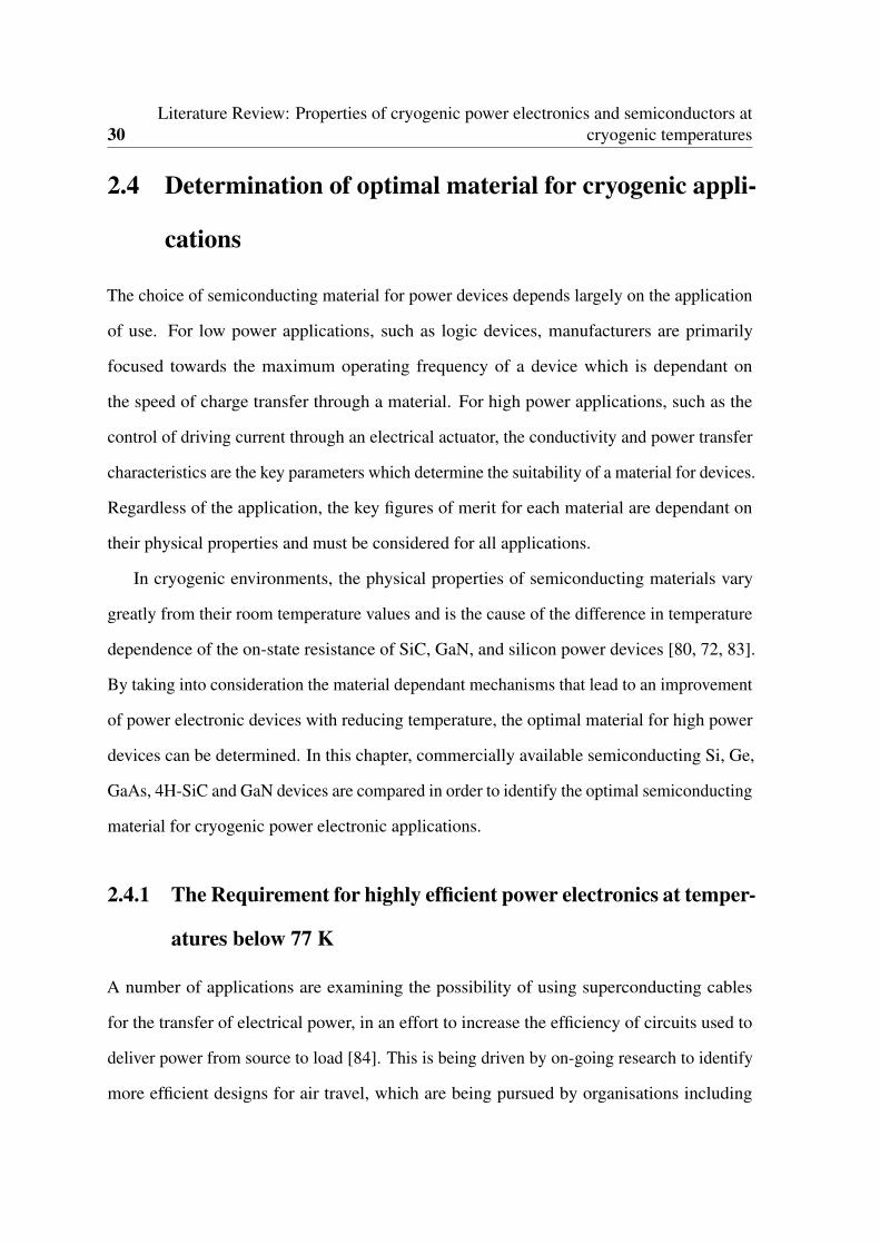
2.5 Temperature Dependence of Bulk Semiconducting Properties 37
where FM is the breakdown field of the material. Assuming a one-sided abrupt junction, the
breakdown voltage for an abrupt PN junction is then given by
VB =εF2
M2qN
(2.16)
where N is the doping concentration of the lightly doped region. The breakdown voltage for
power applications is thus dependent on the ratio of the square of the breakdown field to the
doping concentration. The breakdown field and resulting breakdown voltage as a function
of doping concentration for germanium, silicon, GaAs, 4H-SiC and GaN can be seen in
figure 2.16. The breakdown field for all semiconductors can be seen to increases gradually
by a total factor of two to three times from near intrinsic to heavy doping concentrations. The
breakdown voltage, however, can be seen to decrease near linearly with doping concentration.
The breakdown voltage of germanium is the lowest in comparison to all other materials
whilst the breakdown voltage for SiC and GaN is over a magnitude greater than all other
semiconductors at all doping concentrations. As can be seen from the data, GaN and 4H-SiC
are capable of having a breakdown voltage in excess of 1 kV for doping concentrations at
1014 1015 1016 1017105
106
107
GeSi
GaAs
4H-SiC
GaN
Doping concentration (cm−3)
Bre
akdo
wn
field
(MV
/cm
)
1014 1015 1016 1017101
102
103
104
Doping concentration (cm−3)
Bre
akdo
wn
volta
ge(V
)
Fig. 2.16 Breakdown field (left) and resultant breakdown voltage (right) of Ge [104], Si [23],GaAs [104], 4H-SiC [105] and GaN [106]. Materials for coloured trends on left sub-figurematch that of the right sub-figure.
38Literature Review: Properties of cryogenic power electronics and semiconductors at
cryogenic temperatures
1016 cm−3 whilst PN junctions fabricated from germanium, silicon and GaAs require doping
concentrations well below 1015 cm−3 to achieve a breakdown voltage close to 1 kV.
2.5.3 Drift region resistance at low-temperature
The breakdown voltages illustrated in figure 2.16 assume that the depletion width is free
to extend within the lightly doped drift region indefinitely. In order to allow for this,
manufacturers must add a lightly doped drift region to the all power devices comprising
of typically a lightly doped n-type region that can be seen for all vertical device structures
shown in figures 2.3 and 2.13. In modelling the source of resistive losses within a power
device, it has been shown that the inclusion of this lightly doped drift region contributes
between 50% to over 90% of the total resistive losses within power devices [80, 107, 108].
For the majority of power electronic devices, as the temperature is reduced, the carrier
mobility increases and the total on-state resistance of power electronic devices initially
increases. As the temperature is reduced below 100 K however, materials such as silicon
and SiC experience an exponential increase in resistivity whilst the same does not occur for
germanium and GaAs devices until the temperature is reduced below 20 K.
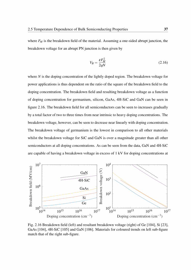
A plot of the resistivity (or the conductivity which is the inverse of resistivity) can be
seen in figure 2.17. As can be seen from the data, the conductivity of the silicon samples
initially increases with decreasing temperature but begins to decrease rapidly for the majority
of samples below 100 K. Below 40 K, the resistivity is two orders of magnitude greater than
that of the room temperature values. In contrast, for germanium, the resistivity continues to
decrease for the majority of samples down to 77 K and even as low as 20 K for the lightly
doped samples. For the majority of samples, the resistivity at 20 K is better or close to the
room temperature value.
For sample 58 in germanium and sample 140 in silicon, the doping concentration exceeds
the degenerate limit and it can be seen that the resistivity remains essentially constant from
2.5 Temperature Dependence of Bulk Semiconducting Properties 39
78 to 10 K. For degenerately doped semiconductors the concentration remains constant as
dopants no longer require energy to be ionised [25]. For all other samples, below 100 K in
silicon and below 20 K in germanium, the exponential increase in resistivity is due to the
freezing out of carriers as the thermal energy of the system in no longer sufficient to ionise all
dopants. The cause in the differing trends of resistivity with reducing temperature is due to
Fig. 2.17 Conductivity of n-type silicon (left) and resistivity of n-type germanium (right)[99, 25] for doping concentrations ranging from <1014 to 1019 cm−3 in silicon and <1014 to5.5×1016 cm−3 in germanium. Doping concentrations are provided for each sample in therespective references based on sample number.
40Literature Review: Properties of cryogenic power electronics and semiconductors at
cryogenic temperatures
the material and dopant type dependence of the carrier freeze out effect. This effect is more
prevalent in materials where dopants have higher ionisation energies such as SiC and GaN.
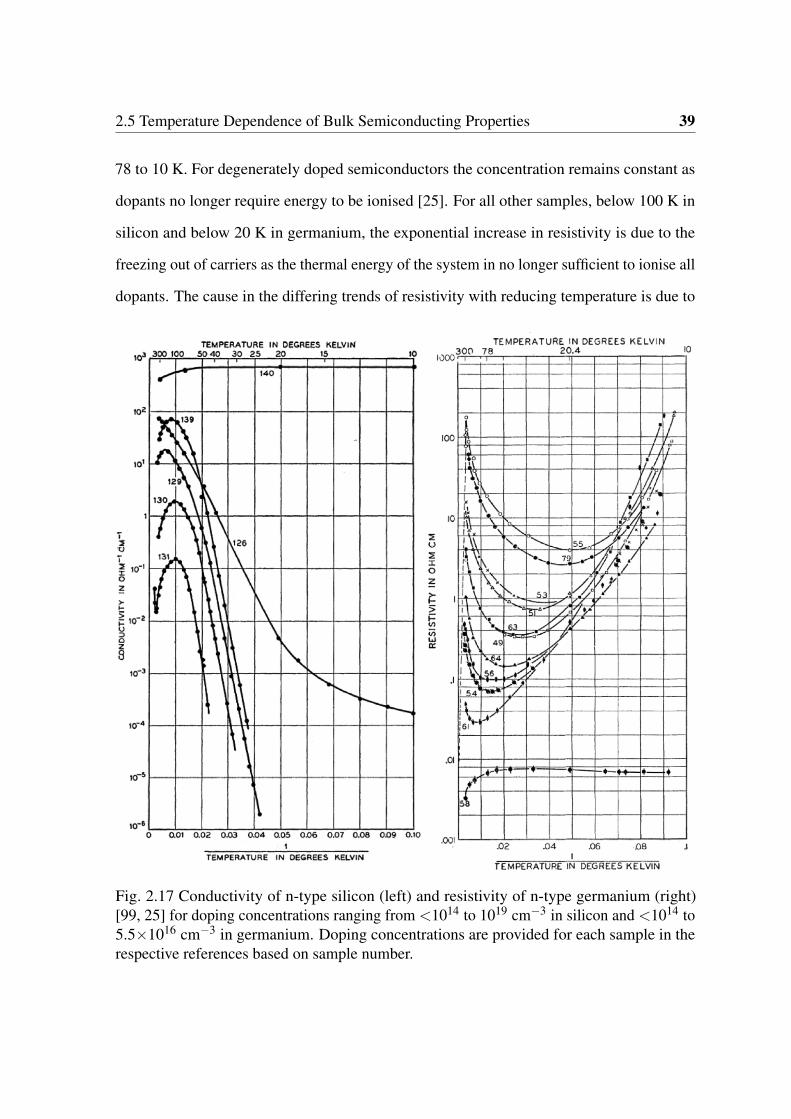
A plot of the measured carrier concentration in 4H-SiC and GaN can be seen in figure 2.18.
For the higher doped samples in SiC, the room temperature carrier concentration is slightly
less than the high-temperature carrier concentration. For highly doped samples above
1017 cm−3 in GaN, the carrier concentration becomes independent of temperature below
50 K which is the result of impurity conduction. Although a high carrier concentration that
is temperature independent is favourable, doping concentrations of this magnitude result in
ultra-low carrier mobilities and a low breakdown voltage.
Analysing data in literature, it can be seen that of all the materials considered here
Germanium and GaAs are the only materials that retain low resistivities and high carrier
mobilities at cryogenic temperatures near 20 K. Of these two materials, GaAs has sufficient
issues involving a high wafer cost, extremely low hole mobility, and critically an inability
to produce native oxides requiring deposition of oxides [111]. Reports on high quality
MOSFETs fabricated from GaAs show issues with gate leakage resulting in low breakdown
voltages and low on-off ratios [112, 113].
Fig. 2.18 Measured free carrier concentration in SiC (left) and GaN (right) as a functionof temperature [109, 110]. Net doping concentrations range from ND - NA = 1.7×10¹⁵ to3.8×1017 cm−3 for SiC and 8×10¹⁶ to 1.8×1017 cm−3 for GaN.
2.5 Temperature Dependence of Bulk Semiconducting Properties 41
On the other hand, germanium has equally high carrier concentrations and mobilities
at low temperatures and also boasts the ability to create a high quality native oxide to the
interface through oxidation of the germanium surface [114, 115, 114]. As far as research
has currently highlighted, the only issue with germanium is that of a low breakdown voltage
that is essential for high power electronics. From this, it can be concluded that although
germanium may not be able to provide power electronics for high voltage applications above
1 kV, it shows the potential to provide high current devices at the lower end of the voltage
scale while still retaining an ultra low on-state resistance.
Thermal conductivity
In highlighting germanium as a superior candidate for low-temperature power electronics,
the issue of thermal management must be analysed. As shown in figure 2.6, during device
operation, the device temperature can exceed the ambient room temperature by more than
100 K if there is poor thermal management. From the transient data, it can be seen that the
silicon devices reached a higher temperature than that of the SiC devices and whilst this may
be simply due to excess resistive losses in the IGBT, it is also due to the thermal conductivity
of the materials used.
The thermal conductivity of a material is a measure of the materials ability to transfer
heat. If the thermal conductivity is high, then a material can cool down quickly after being
heated up in contrast to materials with a low thermal conductivity. At room temperature,
the thermal conductivity of germanium (0.58 W/cmK [116]) is on par with that of GaAs
(0.55 W/cmK [117]) but is low in comparison to silicon, 4H-SiC and GaN (1.3, 3.7 and
1.3 W/cmK respectively [116, 118, 119]) but all increase with reducing temperature.
The thermal conductivity of semiconductors is dependant on the conductivity of phonons
within the material [121]. Phonons are akin to electrons and holes within semiconductors
although they transfer thermal energy as opposed to electrical charge. By eliminating material
42Literature Review: Properties of cryogenic power electronics and semiconductors at
cryogenic temperatures
defects and impurities, the thermal conductivity of the material can be increased. A plot of
the thermal conductivity of germanium and GaN can be seen in figure 2.19 as a function of
temperature. At high temperatures, the main scattering mechanism is that of the Umklapp
process that is inversely proportional to temperature and so by reducing the temperature, the
thermal conductivity of the material increases. At sufficiently low temperatures however,
the thermal conductivity begins to decrease due to a reduction in the thermal capacity of the
material [121, 117]. Aside from these two processes however, the thermal conductivity at
any temperature is reduced following any fabrication process that leads to a dislocation or an
increased impurity concentration as highlighted by the data for GaN.
For power electronic devices, the majority of the heat will be generated in the lightly
doped drift region and so it is the thermal conductivity of this region that is key in maintaining
a low device temperature in operation. Comparing the lightly doped germanium data with
the doped GaN data (labelled 2 in figure 2.19), it can be seen that the thermal conductivity
near 20 K is ∼13 W/cmK for germanium and ∼3 W/cmK for GaN. Silicon and GaAs are
also found to have similar thermal conductivities at 20 K to that of germanium [116, 117]
Fig. 2.19 Thermal conductivity in lightly doped germanium (left) and pure and lightly dopedGaN (right) [116, 120].
2.6 Germanium lateral MOSFETs 43
whilst 4H-SiC is found to reduce with temperature below 100 K resulting in a low thermal
conductivity of ∼0.9 W/cmK at 20 K [118].
2.6 Germanium lateral MOSFETs
As a potential replacement for silicon in CMOS applications owing to it’s superior electron
and hole mobilities, almost all of the published literature on fabricated germanium MOS
devices has been that of a lateral structure with long channels and a heavily doped source and
drain [122–124]. The key issues that have prevented the integration of germanium MOSFETs
into CMOS technology is the quality and longevity of the oxide. Like silicon, germanium
has a native oxide [125] that can be easily fabricated through wet or dry oxidation of the
germanium surface [126, 127]. Unlike SiO2 however, GeO2 is water soluble resulting in
difficulty in fabrication and also requires passivation to protect the device from moisture
within the air.
Recent developments in germanium MOS technology however, have been promising
resulting in germanium p-type and n-type MOSFETs with carrier mobilities that exceed that
of silicon [128, 129]. As well as this, in efforts to increase the current density of the devices,
high-κ dielectrics that incorporate alternative oxides such as Al2O3 and HfO2 have shown
that the native oxide can be successfully encapsulated while also providing a much higher
oxide capacitance [130–132]. As such, the use of germanium in MOS technology is far more
suitable for emerging applications in comparison to years ago than previously thought.
2.6.1 Channel resistance
As the second greatest contributor to overall power device resistance, the resistance of the
channel region at the semiconductor/oxide interface within power MOSFETs must also be
considered [133, 107]. At low drain biases for a long channel device, the drain current of a
44Literature Review: Properties of cryogenic power electronics and semiconductors at
cryogenic temperatures
lateral MOSFET is given by
ID =WL
µeCox
(VG −VT − VD
2
)VD (2.17)
where W/L is the width to length ratio of the gate, Cox is the oxide capacitance and VG, VD
and VT are the gate, drain and threshold voltage respectively. For high drain biases, where the
drain current saturates due to pinch off in the channel, the saturation drain current is given by
ID,sat =WL
µeCox
2(VG −VT )
2 (2.18)
and remains independent of the gate bias assuming that the channel length is greater than
1 µm [134, 135]. From equations (2.17) and (2.18), it can be seen that the drain current is
proportional to the mobility and oxide capacitance of the device and so by maximising their
product the optimal channel resistance can be achieved.
When transistors are in the on-state, the majority of carriers are confined to within 5-
10 nm of the oxide/semiconductor interface [136, 137] and so the effective area of the channel
is extremely thin in comparison to the depth of the p-type region. As well as a reduced
effective area, the mobility of the carriers within the channel is reduced due to increased
scattering from the surface roughness of the oxide/semiconductor interface, trapped charge
at the interface and remote phonons originating from the oxide [138, 139]. As such, a lot of
attention has been focused on maximising the mobility of carriers within the channel whilst
also maximising the oxide capacitance [130, 140].
Of the two parameters, it has been found that the carrier mobility can be increased through
fabrication optimisation but the key parameter is that of the oxide capacitance. The oxide
capacitance for a lateral MOSFET is given by
Cox =εoxAtox
(2.19)
2.6 Germanium lateral MOSFETs 45
where εox is the oxide permittivity and tox is the oxide thickness. For ultrathin oxides, current
leakage from the gate contact becomes a significant issue if the oxide thickness drops below
1 nm [145, 146]. In an attempt to combat the leakage current density through the gate oxides,
alternative gate oxides with higher dielectric constants have been used that offer a thicker
oxide while maintaining an equivalent SiO2 oxide capacitance [147]. The effective oxide
thickness through using alternative high-κ materials is given by
EOT = toxεr,SiO2
εr,high−κ
(2.20)
where εr,SiO2 is the relative dielectric constant of SiO2 (3.9) and εr,high−κ is the relative
dielectric constant of the alternative high-κ material.
An example of the published leakage current density within germanium MOS capacitors
as a function of effective oxide thickness can be seen in figure 2.20. As can be seen from
the data, the reduction in the effective oxide thickness of all gate dielectrics leads to an
exponential increase in leakage current density through the oxide. Comparing the materials
0 0.5 1 1.5 210−9
10−6
10−3
100
103
EOT (nm)
J G@
VF
B+
1V
(A/c
m2 ) [132]
[132][141][142][143][144]
Fig. 2.20 Comparison of leakage current density of germanium MOS capacitors where theGeO2 interlayer has been formed using Pre high-κ O2 plasma (x), post high-κ O2 oxidation(⋄) and Pre high-κ rapid thermal oxidation (). high-κ dielectrics used for germanium MOScapacitors include Al2O3 (Blue), Al2O3/HfO2 (Orange), and ZrO2 (purple).
46Literature Review: Properties of cryogenic power electronics and semiconductors at
cryogenic temperatures
directly, it can be seen that the leakage current density of the ZrO2 dielectrics is much lower
than that of Al2O3 and HfO2 oxide or stacks incorporating Al2O3 and HfO2.
In order for complete control of the gate switching of the device, the leakage through the
gate must be minimised. From the results, it can be seen that ZrO2 with a dielectric constant
of 17-45 [148–150] provides the minimum leakage current density in comparison to Al2O3
and HfO2 devices. There is very little literature available for devices fabricated using ZrO2 in
recent years due to the familiarity of Al2O3 and HfO2 and so here we explore the feasibility
of fabricating high quality ZrO2 through the thermal oxidation of germanium.
2.7 Conclusion
Following this review of power electronic devices at cryogenic temperatures, despite the
initial increase in conductivity of silicon and GaN below room temperature, the exponential
increase in device resistance fabricated from these materials at temperatures below 77 K
warrants them unsuitable for emerging liquid hydrogen applications. It can be seen that,
despite the superior characteristics at room and higher temperatures, the resistance of 4H-SiC
devices increases with decreasing temperature at all temperatures below 300 K. Silicon and
GaN power electronic devices do show improvement below 100 K but this is only true for
MOS and HEMT based devices. Excluding HEMT devices due to longevity issues and high
fabrication costs, the unipolar vertical power MOSFET is the most suitable device for power
electronic applications. Of all the power devices, it has been shown that the resistance of the
lightly doped drift region is the single greatest source of resistive losses in power devices due
to the length and low doping concentration. In order to minimise the resistive losses owing to
this region, a semiconducting material with a high carrier mobility should be chosen. Of the
materials readily available for commercial use, germanium appears to be the most suitable
due to an extremely high carrier mobility at 20 K of over 106 cm2/Vs which far exceeds
the bulk carrier mobilities of silicon, 4H-SiC and GaN at the same temperature. Recent
2.7 Conclusion 47
developments in germanium MOS technology also show promise for incorporating high-κ
gate dielectrics to maximise the current density within germanium devices while retaining a
simple fabrication approach that can be readily be achieved using an atomic layer deposition
(ALD) or thermal oxidation approach.
As such, germanium appears as a promising candidate for low resistance, fast switch-
ing, power electronics for liquid hydrogen applications. Despite this, a significant lack of
experimental or modelling work on the physical properties of germanium have prevented a
conclusive study on the viability of germanium power electronics at low temperatures. In
order to correct for this, the experimental data reported for germanium must be analysed
and modelled in order to allow for a device simulation of a high power vertical germanium
MOSFET at 20 K.
Chapter 3
Modelling the Cryogenic Properties of
Germanium for Device Simulation
3.1 Introduction
The choice of semiconducting material for power devices critically depends on the intended
application. For low power applications, such as logic devices, manufacturers are primarily
focused on maximising the operating frequency of a device, which is dependent on the rate
of charge transfer through a material. For high power applications, such as the control of
driving an electrical actuator, the conductivity and carrier lifetimes are the key parameters
which must also be considered when determining the suitability of a material for devices.
In cryogenic environments, the physical properties of semiconducting materials vary
greatly from their room temperature values. Despite the maturity and development of
commercially available silicon and more recently SiC and GaN, electrical characterisation
at cryogenic temperatures below 100 K shows that devices fabricated from these materials
are unsuitable for cryogenic applications due to the exponential increase in the resistance of
these devices. Unlike silicon, SiC and GaN, semiconducting germanium does not experience
the same increase in resistance until the temperature is reduced below 20 K and devices
50 Modelling the Cryogenic Properties of Germanium for Device Simulation
fabricated from germanium have even been shown to function at 4.2 K with similar electrical
characteristics to that at room temperature.
Despite this benefit, the electrical properties of germanium and germanium devices
have yet to be modelled and the only benchmark for considering germanium devices for
applications is by analysing characteristics from literature. As such, this chapter will focus on
modelling the physical characteristics of germanium from literature and analysing the impact
of its properties including carrier mobility, velocity saturation, free carrier concentration and
minority carrier lifetime.
3.2 Closed-loop analytical model
The closed-loop analytical model which is developed in this chapter is based on the de-
termination of the total carrier concentration and carrier mobility for a range of dopant
concentrations that are relevant to power electronic devices over a range of temperatures.
The total current density J through a semiconducting material can be expressed as
J = σF (3.1)
where F is the applied electric field and σ is the conductivity. The conductivity is related to
the free carrier concentration and carrier mobility according to
σ = nqµe + pqµh (3.2)
In certain regions of semiconductor devices, the concentration of electrons may be many
orders of magnitudes greater than the concentration of holes or vice versa. In such instances,
3.3 Carrier concentration 51
the conductivity can be approximated to
σn = nqµe|n>p (3.3a)
σp = pqµh|p>n (3.3b)
for n-type and p-type material respectively.
For unipolar devices such as junction field effect transistors (JFETs) and MOSFETs, the
total current given by equation 3.1 can be calculated using the conductivity given by either
equation 3.3a or 3.3b as only electrons or holes contribute to the total current density for
unipolar n-type or p-type FETs. As such, the temperature, doping and field dependence
of electrons and holes will be considered independently when modelling experimental
results for unipolar devices. For bipolar devices such as PiN diodes and IGBTs, the total
current of the devices is dependent on the sum of the electron and hole currents and so
both equation 3.3a and 3.3b must be combined. For these devices, it is the conductivity
of the minority carrier concentration which dominates the overall device conductivity and
so generation and recombination effects must be taken into consideration when simulating
device behaviour.
3.3 Carrier concentration
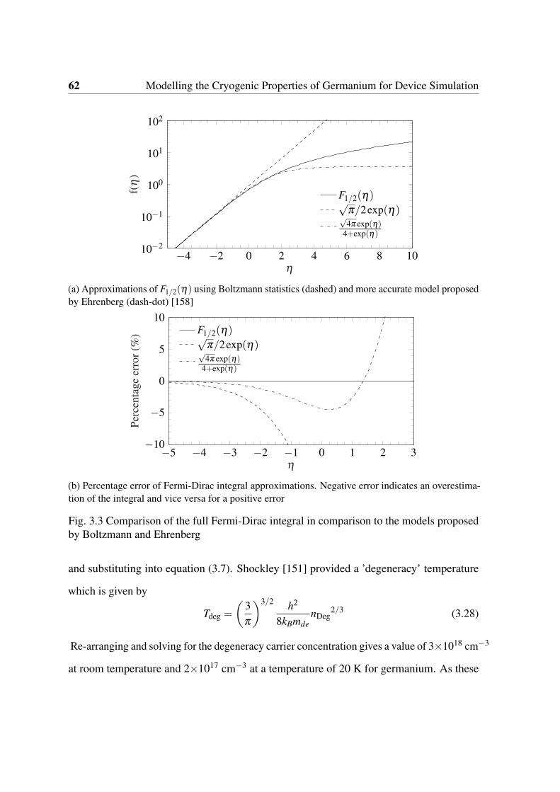
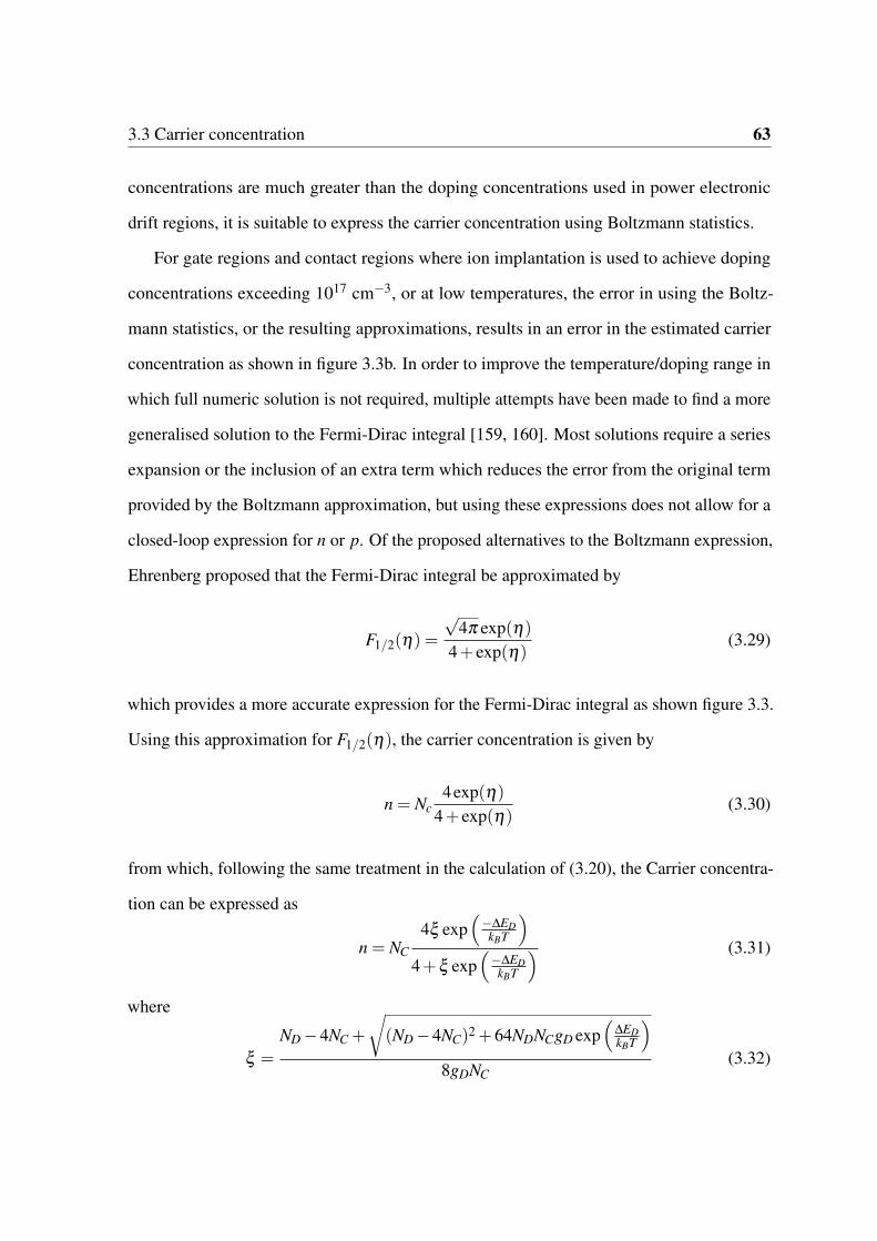
At temperatures above absolute zero, the concentration of free carriers that are available for
conduction is given by [151]
n(T ) =∫
∞
EC
N (E) f (E,T )dE (3.4)
52 Modelling the Cryogenic Properties of Germanium for Device Simulation
where T is the absolute temperature, N (E) is the density of states and f (E,T ) is the Fermi-
Dirac occupational probability which is given by
f (E,T ) =1
1+ exp(
E−EFkBT
) (3.5)
where E is the energy, EF is the Fermi energy and kB is Boltzmann’s constant. The Fermi-
Dirac occupational probability describes the probability of an energy level being occupied
by an electron. At the energy denoted by EF , the probability of occupation is 50%. For
cryogenic applications, where the free carrier density is low as a result of the temperature,
the parabolic-band approximation can be applied [152] as the majority of carriers are located
at the conduction band edge. As such, the density of states is given by
N (E) = MC
√2
π2m1.5
de (E −EC)0.5
ℏ3 (3.6)
where MC is the number of equivalent minima in the conduction band, mde is the electron
density of states effective mass, EC is the energy of the conduction band edge and ℏ= h/2π
is the reduced Planck’s constant.
Through the use of the parabolic band approximation, the total carrier concentration can
be expressed as
n = NC2√π
F1/2
(EF −EC
kBT
)(3.7)
where NC is the density of states in the conduction band given by
NC = 2(
2πmdekBTh2
)3/2
MC (3.8)
F1/2 is the Fermi-Dirac integral of order 12 which is given by
F1/2(η) =∫
∞
0
α1/2
1+ exp(α −η)dα (3.9)
3.3 Carrier concentration 53
where in η is the reduced Fermi-energy equal to (EF −EC)/kBT and α is (E −EC)/kBT .
No closed-loop solutions of equation (3.9) exist and a closed-loop approximation can only
be generated when the Fermi energy in a semiconductor is several kBT below the conduction
band edge. In such instances, Fermi-Dirac integral of order 12 can be approximated to an
exponential of the form
F1/2(η) =
√π
2exp(η) (3.10)
and so equation (3.7) can be expressed as
n = NC exp(−EC −EF
kBT
)(3.11)
The hole concentration in a semiconductor can be described in a similar manner with
p(T ) =∫ EV
∞
N (E)(1− f (E,T ))dE (3.12)
where EV is the valence band energy and the term (1− f (E,T )) is the probability of the
energy level E being occupied by a hole. Solving equation (3.12) using the same Boltzmann
approximation leads to
p = NV exp(−EF −EV
kBT
)(3.13)
where NV is the density of states in the valence band given by
NV = 2(
2πmdhkBTh2
)3/2
(3.14)
where mdh is the density of states effective mass of the valence band.
At cryogenic temperatures, the functionality of devices crucially depends on the con-
centration of extrinsic carriers that are available for conduction. Doping a semiconductor
with an impurity atom produces an energy level within the band gap of the material from
which carriers can be excited from or decay to. For impurities such as antimony or arsenic in
54 Modelling the Cryogenic Properties of Germanium for Device Simulation
germanium, the donor energy ED is a single energy level below the conduction band and the
concentration of electrons at the energy level is
n = N(ED) f (ED,T ) (3.15)
For a single donor level, the density of states at the energy ED is equal to the doping
concentration and the carrier concentration at the donor level is given by
n = ND1
1+g−1D exp
(ED−EF
kBT
) (3.16)
where gD is the electron degeneracy factor of the donor energy level given by ED. The
concentration of ionised donors is therefore given by
n(ED) = N(ED)(1− f (ED,T )) (3.17)
which is equal to
N+D = ND
1
1+gD exp(−ED−EF
kBT
) (3.18)
At cryogenic temperatures where the intrinsic carrier concentration is negligible in
comparison to the donor concentration, it can be assumed that the free electron and ionised
donor concentrations given by equations (3.11) and (3.18) are equal. By equating these two
expressions, the Fermi-level can algebraically be expressed as
exp(
EF
kBT
)=
−1+√
1+4NDNC
gD exp(
EC−EDkBT
)2gD exp
(−EDkBT
) (3.19)
3.3 Carrier concentration 55
Substituting this expression for the Fermi-energy into equation (3.11) gives a Fermi-energy
independent electron concentration equal to
n =
NC
(√1+4ND
NCgD exp
(∆EDkBT
)−1)
2gD exp(
∆EDkBT
) (3.20)
where ∆ED is the difference between the conduction band minimum and donor energy level.
For the free hole concentration, the same treatment results in
p =
NV
(√1+4 NA
NVgA exp
(∆EAkBT
)−1)
2gA exp(
∆EAkBT
) (3.21)
where ∆EA is the difference between the acceptor energy level and the valence band and gA
is the hole degeneracy factor.
At temperatures where the thermal energy is lower than the energy required to ionise an
electron from the donor energy level to the conduction band, the free electron concentration
exponentially decreases and can be approximated by
n =
√NDNC
gDexp(− ∆ED
2kBT
)(3.22)
A plot of log(n) against 1/T results in a linear freeze-out region with a gradient equal to
ED/2. Knowing this, it is possible to extract the ionisation energy of impurities in the
semiconductor which was used to obtain an ionisation energy of 12.5 meV for antimony in
germanium.
In the instance that multiple impurity atoms are present within the semiconductor, it
is possible for the carrier concentration to be equal to the sum of all ionised impurities
present within the material. If the semiconductor contains impurities with different ionisation
energies, equation (3.18) must be modified to take into consideration the presence of multiple
56 Modelling the Cryogenic Properties of Germanium for Device Simulation
impurity atoms. Doing so results in the transcendental equation
NC exp(−EC −EF
kBT
)= ∑
x
ND,x
1+gD exp(−ED,x−EF
kBT
) (3.23)
where x is equal to the number of donor levels and ND,x and ED,x represent the concentration
and energy level of impurity x. In the presence of multiple energy levels, the Fermi energy
must be solved numerically using equation (3.23) and the carrier concentration can be
calculated via substitution of EF into equation (3.11). Commonly used dopants such as
antimony for n-type germanium and boron for p-type germanium have a single shallow
ionisation energy close to the conduction and valence band edge respectively, and so the
approximation for the carrier concentration given by equation (3.20) can be used. In regions
close to contacts, or oxide/semiconductor interfaces, the presence of oxygen, or metallic
impurities such as chromium, gold, or silver can introduce multiple ionisation energies within
the band gap and so the calculation of the carrier concentration must be completed through
solving for EF using equation (3.23).
3.3.1 Model comparison to experimental measurements
At cryogenic temperatures, the primary cause of device failure is related to the reduction of
thermal energy in the system, resulting in a reduction in the number of ionised donors. An
example of the ionised dopant concentration for germanium, silicon and 4H-SiC is plotted
in figure 3.1. From the figure, it can be seen that the total ionised dopant concentration
tends towards equation (3.22) (in the temperature range where the thermal energy becomes
insufficient to ionise all dopants). The rate of decay is inversely proportional to the ionisation
energy which is high for 4H-SiC and low for germanium. As such, although nitrogen in
4H-SiC has a high ionisation energy in comparison to antimony in germanium, the reduction
of ionised donors can be seen to decrease gradually in comparison.
3.3 Carrier concentration 57
0 20 40 60 80 100 120 140 160 180 2001012
1013
1014
1015
1016
Temperature (K)
Ele
ctro
nco
ncen
trat
ion
(cm
−3 )
7.5×1015 cm−3
1.5×1015 cm−3
9.3×1014 cm−3
1.2×1014 cm−3
(a) Calculated electron concentration for different net acceptor concentrations compared to experi-mental data [25, 153].
0 20 40 60 80 100 120 140 160 180 2001012
1013
1014
1015
1016
1017
Temperature (K)
Hol
eco
ncen
trat
ion
(cm
−3 )
2.4×1016 cm−3
9.0×1015 cm−3
1.4×1015 cm−3
7.5×1014 cm−3
(b) Calculated hole concentration for different net acceptor concentrations compared to experimentaldata [154]
Fig. 3.1 Comparison of the free electron and hole concentration models to experimental datain n-type (a) and p-type (b) germanium using equations (3.25) and (3.26) in equations (3.20)and (3.21) with density of states effective masses of 0.22 and 0.34 for electrons and holesrespectively.
58 Modelling the Cryogenic Properties of Germanium for Device Simulation
At doping concentrations greater than 1016 cm−3, an impurity band centred at the donor
energy begins to form which results in a reduction of the ionisation effective energy [155, 25].
For silicon and 4H-SiC [155, 98, 156, 157], the effective ionisation energy for both acceptors
and donors energy can be modelled using
EA/D,eff = EA/D,0 −αN1/3net (3.24)
where EA/D,0 is the ionisation energy for acceptors/donors at low doping concentrations,
α is a fitting constant and Nnet is the sum of the acceptor and doping concentration [155].
Based on fitting the electron concentration to experimental data, Eq. (3.26) overestimates the
reduction in ionisation energy and the ionisation energy of antimony doped Ge was found to
(a) Comparison of uncompensated model for different ionisation energies where the increasingionisation energy reduces carrier concentration at low temperatures
(b) Comparison of uncompensated model (solid) to compensated extrinsic model (dashed)
Fig. 3.2 Richardson plot of carrier concentration in floatzone grown germanium of low andmoderate doping concentrations [25].
comparing the samples, it can be seen that samples with higher doping concentrations are
less affected by the presence of compensating carriers. The error in the freeze-out rate of
the sample with a net doping concentration of 5.5×1016 cm−3 can be corrected by assuming
3.3 Carrier concentration 61
the ionisation varies from 10 to 11 meV as the temperature decreases. For the lightly doped
sample however, the variation in ionisation is larger rising from 14 to 16 meV.
In order to accurately model the carrier concentration for doping concentrations with com-
pensation ratios greater than 10%, in the carrier freeze-out region, the carrier concentration
must be related to the temperature through
n(NA +n)ND −NA −n
=NC
gDexp(−∆ED
kBT
)(3.27)
from which, the carrier concentration can be solved numerically using the acceptor concen-
tration and the density of states effective mass as a fitting parameter. Using a density of
states effective mass of mde = 0.3m0 gives an acceptor concentration of 1×1013 cm−3 and
1.3×1014 cm−3 which correspond to compensation ratios of ND/NA ≈ 0.1 for both samples.
It can be seen that the presence of compensating acceptor impurities results in a carrier
freeze-out temperature slope that deviates from that predicted from equation (3.20). In the
case where NA is negligible in comparison to both n and ND, the expression for the carrier
concentration in equation (3.27) collapses to equation (3.22).
3.3.3 Degeneracy
The models for the carrier concentration given by equations (3.11), (3.20) and (3.27) assume
that the application of Boltzmann statistics is suitable for simulating device behaviour.
Boltzmann statistics apply in the assumption that Fermi energy within the band gap is at
least several kBT below the conduction or above the valence band edge, from which, the
Fermi-Dirac integral can be approximated by equation (3.10) as shown in figure 3.3a. If the
doping concentration is great enough, or if the temperature is low enough, this approximation
no longer holds and the carrier concentration will deviate from equation (3.11). In such an
instance, the carrier concentration must be calculated numerically by solving equation (3.9)
62 Modelling the Cryogenic Properties of Germanium for Device Simulation
−4 −2 0 2 4 6 8 1010−2
10−1
100
101
102
η
f(η
)
F1/2(η)√π/2exp(η)
√4π exp(η)
4+exp(η)
(a) Approximations of F1/2(η) using Boltzmann statistics (dashed) and more accurate model proposedby Ehrenberg (dash-dot) [158]
−5 −4 −3 −2 −1 0 1 2 3−10
−5
0
5
10
η
Perc
enta
geer
ror(
%) F1/2(η)√
π/2exp(η)√
4π exp(η)4+exp(η)
(b) Percentage error of Fermi-Dirac integral approximations. Negative error indicates an overestima-tion of the integral and vice versa for a positive error
Fig. 3.3 Comparison of the full Fermi-Dirac integral in comparison to the models proposedby Boltzmann and Ehrenberg
and substituting into equation (3.7). Shockley [151] provided a ’degeneracy’ temperature
which is given by
Tdeg =
(3π
)3/2 h2
8kBmdenDeg
2/3 (3.28)
Re-arranging and solving for the degeneracy carrier concentration gives a value of 3×1018 cm−3
at room temperature and 2×1017 cm−3 at a temperature of 20 K for germanium. As these
3.3 Carrier concentration 63
concentrations are much greater than the doping concentrations used in power electronic
drift regions, it is suitable to express the carrier concentration using Boltzmann statistics.
For gate regions and contact regions where ion implantation is used to achieve doping
concentrations exceeding 1017 cm−3, or at low temperatures, the error in using the Boltz-
mann statistics, or the resulting approximations, results in an error in the estimated carrier
concentration as shown in figure 3.3b. In order to improve the temperature/doping range in
which full numeric solution is not required, multiple attempts have been made to find a more
generalised solution to the Fermi-Dirac integral [159, 160]. Most solutions require a series
expansion or the inclusion of an extra term which reduces the error from the original term
provided by the Boltzmann approximation, but using these expressions does not allow for a
closed-loop expression for n or p. Of the proposed alternatives to the Boltzmann expression,
Ehrenberg proposed that the Fermi-Dirac integral be approximated by
F1/2(η) =
√4π exp(η)
4+ exp(η)(3.29)
which provides a more accurate expression for the Fermi-Dirac integral as shown figure 3.3.
Using this approximation for F1/2(η), the carrier concentration is given by
n = Nc4exp(η)
4+ exp(η)(3.30)
from which, following the same treatment in the calculation of (3.20), the Carrier concentra-
tion can be expressed as
n = NC
4ξ exp(−∆EDkBT
)4+ξ exp
(−∆EDkBT
) (3.31)
where
ξ =
ND −4NC +
√(ND −4NC)2 +64NDNCgD exp
(∆EDkBT
)8gDNC
(3.32)
64 Modelling the Cryogenic Properties of Germanium for Device Simulation
Using this form for calculating the carrier density increases the estimated carrier concentration
at low temperatures for highly doped samples but still underestimates the carrier density by
over an order of magnitude at cryogenic temperatures.
As the majority of power electronic devices have lightly doped regions for high breakdown
voltages, the majority of the device can be modelled using equation (3.20). The use of
equation (3.31) scarcely improves the accuracy of the carrier concentration. As a result of
this, Fermi statistics must be applied, or it must be assumed that all carriers are ionised for
regions where the carrier density is in excess of 1017 cm−3.
3.4 Carrier mobility
The mobility of electrons and holes in semiconductors greatly differs from room tempera-
ture values at cryogenic temperatures. At cryogenic temperatures, there is a reduction of
scattering from phonons which results in an increase in carrier mobility for lightly doped
semiconductors. This reduction in scattering increases the mobility of carriers leading to
an increase in conductivity and the maximum switching frequency of devices. Combined
with the knowledge of the conductivity from equation (3.2), the importance of a high carrier
mobility cannot be understated as this ensures a fast device with low resistive losses.
The mobility of carriers in a material with multiple scattering mechanisms can be calcu-
lated using Matthiessen’s rule [161]
1µtot
=j
∑1
1µ1
+1µ2
+ ...+1µ j
(3.33)
where each µ j represents a different mobility mechanism.
At room temperature, the dominant scattering for unintentionally doped germanium is
that of lattice scattering from acoustic phonons which for non-polar semiconductors is given
3.4 Carrier mobility 65
by [162, 163]
µac =2√
2πqℏ4Cl
3E2dsm
∗5/2 (kBT )3/2 (3.34)
where Cl is the longitudinal elastic constant and Eds is the displacement of the band edge per
unit dilation of the lattice which is induced by the acoustic phonon and m∗ is the effective
mass.
The scattering rate resulting from optical phonons becomes considerable for carriers with
higher energy and can be approximated to [164]
µop =
√2qℏ3Cl
m∗5/2E2opωop
[exp[
θop
T
]−1][√
E + kBθop + exp[
θop
T
]√E − kBθop
]−1
(3.35)
where E is the carrier energy, Eop is the optical phonon deformation potential, ωop is the
angular frequency of the optical phonons and θop is equivalent optical phonon temperature.
Following work by Debye [25], it can be shown that the scattering of carriers due to optical
phonons is greatest for carriers with energies close to 3kBT and so an approximation of
the optical phonon limited carrier mobility can be taken by assuming E = 3kBT . Making
this substitution for the carrier energy and performing a best fit between the model and the
experimental data gives a value of 0.42 eV for the optical phonon deformation potential and
is in agreement with previously published results in germanium [164].
For doped regions at cryogenic temperatures, the dominant scattering mechanisms are
ionised and neutral impurity scattering. The potential generated by an ionised impurity
generates a charged region which scatters carriers that come within its vicinity during
conduction. The carrier mobility for ionised impurity dominated transport is given by [165]
µii =27/2ε2 (kBT )3/2
π3/2m∗1/2(n+2NA)Z2q3
(ln(
1+3εkBTn′1/3q2
))−1
(3.36)
66 Modelling the Cryogenic Properties of Germanium for Device Simulation
where Z is the charge of the impurity atom in units of q, n+2NA the concentration of ionised
impurities and n′ represents the ionised donor screening concentration given by
n′ = n+(ND −NA −n)(n+ND)
ND(3.37)
The 2NA term in the total concentration of ionised impurities arises from the fact that, in a
compensated material, electrons from an energy level of ED will be trapped by a compensating
energy level EA. The transfer of an electron from a donor atom to an acceptor atom will leave
both impurities ionised with an opposite net charge. It is assumed that the polarity of this
charge does not affect the overall scattering rate and the total number of ionised impurities
from this compensation will be equal to 2NA.
During the fabrication process, it is possible for small concentration of unintentional
impurities such as oxygen and nitrogen to enter the lattice leading to a perturbation of the
lattice periodicity. These impurities tend to remain uncharged as they require much larger
ionisation energies. As well as unintentional impurities, at temperatures where carriers begin
to freeze out, the resulting dopant atoms have a resultant neutral charge. Despite the neutral
charge, the perturbation of the lattice scatters carriers that come into close proximity of
the impurity. Commonly, the mobility of carriers limited by neutral impurity scattering is
expressed using the model developed by Erginsoy [166, 167]
µneu =1
A(E)m∗q3
εNneuℏ3 (3.38)
where Nneu is the concentration of neutral impurities, taken to be equal to ND −NA −n, and
A(E) is a function which takes into consideration the interaction of neutral impurities with
carriers of varying energy [168]. Although fabricated devices do contain a concentration of
unintentional impurities such as nitrogen and/or oxygen, these will not be considered in Nneu
as the concentration of neutral dopants resulting from carrier freeze-out greatly exceeds the
3.4 Carrier mobility 67
concentration of unintentional impurities that are present from the fabrication process [169].
In determining A(E), Erginsoy proposed that the interaction of neutral impurities with carriers
could be assumed to be independent of the energy of the carriers and replaced this function
with the modal value of 20 [166]. For higher temperatures, this assumption has shown to be
more than satisfactory in silicon and 4H-SiC [101, 156, 170] where the majority of carriers
have a lower kinetic energy. For germanium at temperatures below 20 K however, it has
been shown [167] that energy dependence of the neutral impurity scattering rate must be
taken into consideration as the value for A(E) reduces monotonically with increasing carrier
energy. This has also been shown to be the case for highly doped silicon [168, 171].
For modelling the mobility of carriers in germanium at temperatures below 20 K, the
scattering from neutral impurities must be considered [167]. However, it shall be shown in
the forthcoming section that the influence from neutral impurities can be neglected if it is
assumed that all dopants remained ionised from 20 K to room temperature.
3.4.1 Model comparison to experimental results
Combining equations (3.34) to (3.38) using equation (3.33) allows a computational model
for the electron mobility of a non-degenerate semiconductor to be determined from room
temperature down to 20 K. At temperatures above room temperature, additional scattering
mechanisms such as carrier-carrier scattering must be considered [26]. This mechanism may
Table 3.1 Parameters used to calculate the electron mobility for intrinsic and n-type germa-nium in figure 3.4
68 Modelling the Cryogenic Properties of Germanium for Device Simulation
be safely ignored for the temperature range that is the focus of this study. During device
fabrication, unintentional defects and impurities lead to excess scattering and hence carrier
mobilities that are lower than theoretical predictions and cannot be predicted with high levels
of certainty until device fabrication has been completed.
The experimental electron mobility as a function of temperature for intrinsic and n-type
germanium is plotted in figure 3.4 where the reported values for ND −NA are 1013 and
5.6×1016 cm−3 based on hall measurements. Calculating the total mobility for both of these
materials results in the solid line shown in the figures.
From the data in figure 3.4a, it can be seen that the total carrier mobility in lightly
doped germanium is dominated by the harmonic average of the acoustic and optical phonon
limited mobilities. The harmonic average of the acoustic and optical phonon scattering using
equation (3.33) is more than satisfactory for modelling electrons in intrinsic germanium.
For the moderately doped sample, it can be seen that scattering from ionised impurities is
grossly overestimated by over an order of magnitude at 20 K although the error is negligible
for temperatures above 200 K. It should also be noted that the scattering from neutral
impurities has not been considered for these calculations as has previously been shown
that the presence of neutral impurities is only required for modelling at temperatures below
20 K [173, 167]. Despite the neglect of neutral impurity scattering, which would only serve
to further lower the predicted mobility, the overestimation of the scattering from ionised
impurities makes the harmonic average approximation unsuitable for modelling of carriers at
cryogenic temperatures.
3.4.2 Higher accuracy mobility modelling
As shown, the harmonic averaging of the carrier mobility provides a satisfactory fit for
mobility data for doping concentrations at and below 5.5×1016 cm−3 for temperatures
above 200 K. For higher doping concentrations however and lower temperatures, the model
3.4 Carrier mobility 69
0 50 100 150 200 250 300103
104
105
106
µii
µop
µac
Temperature (K)
Mob
ility
(cm
2 /Vs)
µtoti-Ge [172]
(a) ND −NA = 1×1013 cm−3
0 50 100 150 200 250 300102
103
104
105
µac µop
µii
Temperature (K)
Mob
ility
(cm
2 /Vs)
µtotn-Ge [25]
(b) ND −NA = 5.5×1016 cm−3
Fig. 3.4 Calculated electron mobility in intrinsic (a) and n-type (b) germanium comparedto experimental data. Dashed lines indicate individual scattering mobilities and solid linerepresent to the harmonic average of these mobilities.
begins to underestimate the carrier mobility compared to experimental data as can be seen
in figure 3.4b. The mobilities provided through equations (3.34) to (3.38) were derived
assuming all carriers have an energy of 3kBT for reasons which shall be explained herein.
70 Modelling the Cryogenic Properties of Germanium for Device Simulation
The carrier mobility of a semiconductor is given by
µ =q⟨τ⟩
m(3.39)
where τ is the energy relaxation time of carriers which can be solved for through
1τ(x)
= ∑n
1τn(x)
(3.40)
in a similar to manner the calculation of the carrier mobility through the harmonic average
model. The expectation values for τ can be found through the numerical solving of
⟨τ⟩=∫
∞
0 τ(x)e−xx3/2dx∫∞
0 e−xx3/2dx=
43√
π
∫∞
0τ(x)e−xx3/2 (3.41)
where x = E/kBT is the normalised carrier energy.
For temperatures below 150 K, the majority of scattering arises from acoustic phonons
and ionised impurities. Assuming neutral impurities and optical phonons can be neglected
from the calculation of τ , the expectation value becomes
⟨τ⟩= 43√
π
∫∞
0
e−xx3/2
τ−1ac (x)+ τ
−1ii (x)
dx (3.42)
where the scattering rates are given by
τac =ll
vtx1/2 (3.43)
and
τii = B(x)v3t x3/2 (3.44)
where vt is given by
vt =
√2kBTm∗ , (3.45)
3.4 Carrier mobility 71
ll is acoustic scattering length given by
ll =πℏ4Cl
m∗2E2dskBT
(3.46)
and
B(x) =m∗ε2
2π(n+2NA)q31
ln(
1+(
εxq2n′1/3
)2) (3.47)
In order for a closed-loop model for (3.42) to be determined, the B(x) term must be substituted
with a constant which is independent of x. Originally, it was found that if the expectation
value for τ was calculated at temperatures where ionised impurity scattering dominates, that
is assuming τ ≈ τii, then the integrand of equation (3.41) has a maximum at x = 3. As a
result, it became common practice to calculate the relaxation time was through substituting
B(x) with B(3). Through the substitution of B(x)≈ B(3), a closed-loop expression for the
acoustic phonon and ionised impurity limited relaxation time was found to be [25]
τac-ii = τac[1+ z2(Ci(z)cos(z)+Si(z)sin(z)− π
2sin(z))] (3.48)
where
z2 =6τac
τii(3.49)
where the mobility was calculated through multiplying the previously calculated relaxation
time by q/m∗.
Debye and Conwell showed that the approximation of B(x) ≈ B(3) allowed for the
resistivity of germanium to be modelled in the temperature range of 77 to 300 K with doping
concentrations ranging from 1014 to 5.5×1016 cm−3 when only considering acoustic and
ionised impurity scattering. At low temperatures, the consideration from neutral impurities
72 Modelling the Cryogenic Properties of Germanium for Device Simulation
1013 1014 1015 1016 1017 1018 1019 1020101
102
103
104
105
106
Net doping concentration (cm−3)
Ele
ctro
nm
obili
ty(c
m2 /V
s) T = 20 KT = 77 KT = 300 K
(a) Mobility model using harmonic average (dashed) and model developed by Debye and Conwell(solid) where both models substitute B(x) with B(3) in order to achieve equation (3.36) from (3.44)
1013 1014 1015 1016 1017 1018 1019 1020101
102
103
104
105
106
Net doping concentration (cm−3)
Ele
ctro
nm
obili
ty(c
m2 /V
s) T = 20 KT = 77 KT = 300 K
(b) Mobility model for electrons in germanium using full numerical solution for equations (3.39) and(3.41)
Fig. 3.5 Comparison of the mobility models for germanium at room temperature [174],77 K [174] and 20 K [25]. Calculations were performed using an effective mass ofm∗ = 0.22m0. Solid or dashed lines are based on the discussed models and data pointsare taken from references.
was added by assuming that
1µDeb-Con
=1
µac-ii+
1µNeu
(3.50)
3.4 Carrier mobility 73
although the presence of neutral impurities is only required for mobility modelling below
20 K [175].
A plot of the experimental carrier mobility in germanium in comparison to equa-
tions (3.33) and (3.48) can be seen in figure 3.5a. From the figure, it can be seen that
the scattering from ionised impurities is overestimated at higher doping concentrations as the
predicted mobility is lower than experimental values at room temperature once the doping
concentration exceeds 1017 cm−3. For lower doping concentrations, where the majority of
scattering is dominated by optical and acoustic phonons, the harmonic average is suitable
for predicting the carrier mobility. At lower temperatures, the range of suitability for these
two models is reduced and it can be seen that the models underestimate the mobility for
doping concentrations above 1015 cm−3 and 1013 cm−3 respectively at 77 K and 20 K. It can
readily be seen from the data that the use of either the harmonic average model or the model
provided by Conwell and Debye is unsuitable for carrier mobility modelling at cryogenic
temperatures.
In comparison to these two approximation models, the carrier mobility predicted as a
function of doping using the full numeric solution of equations (3.41) and (3.39) is plotted in
figure 3.5b. The scattering from neutral impurities was not considered in this calculation and
it can be seen that this does not reduce the accuracy of the model even at temperatures down
to 20 K for the data presented.
For the purposes of the data considered in figure 3.5, it was assumed that all donors
remain ionised and the acceptor concentration was negligible in all cases, resulting in n = ND.
With this assumption, the effective mass was found to best fit the data with an effective
mass of m∗ = 0.22m0 which is in agreement with the data for modelling carrier mobility in
germanium [25, 176, 167]. If carrier freeze-out was to be included within the model, then
the contribution from neutral impurities must be considered.
74 Modelling the Cryogenic Properties of Germanium for Device Simulation
Comparing the full numerical solution to the approximations, it can be seen that all
three models converge to the same value for lattice scattering limited mobility at low doping
concentrations. Where the full numeric solution has an advantage in terms of accuracy,
the simplicity of equations (3.33) and (3.48) is attractive for reducing computation time in
simulations. In order to find the range of suitability of both equation (3.33) and (3.48), the
error in comparison to model has been calculated using
%Error = 100(
µnum −µapp
µapp
)= 100
(⟨τ⟩− τapp
τapp
)(3.51)
where τapp is the approximation of the scattering rate given by equation (3.40) or (3.42) and
is plotted in figure 3.6 as a function of temperature. It can be seen that for room temperature
modelling, there is less than a 1% deviation between the full numeric model for doping
concentrations less than 1014 cm−3 although the error is increased to over 10% at 20 K. Of
0 50 100 150 200 250 3001010
1011
1012
1013
1014
1015
1016
1017
1018
Temperature (K)
Dop
ing
conc
entr
atio
n(c
m−
3 )
1% Error5% Error10% Error
Fig. 3.6 Comparison of percentage error between approximations of the harmonic average(blue) and the model prepared by Debye and Conwell (orange) with respect to the fullnumerical solution for the carrier mobility. The error lines indicate doping concentration atwhich there is a 1% (solid), 5% (dashed) and 10% (dash-dot). Above the percentage errorlines, the full numeric solution must be performed to calculate the carrier mobility.
3.4 Carrier mobility 75
the two models, it can be seen that the harmonic average model follows the full numeric
solution for a higher range of doping compared to the Debye-Conwell model. For accurate
modelling of carrier mobility at 20 K, a full numeric solution must be applied.
3.4.3 Empirical mobility model
Neglecting oxide/semiconductor interfaces which shall be considered later, computation
of the carrier concentration and mobility in order to determine the conductivity, and the
resulting current density can be quickly achieved for a single piece of material using the
aforementioned models. However, simulating the current density at specific regions of a
device where carrier densities and electric field vary as a function of position requires far
more numerical effort. TCAD is a family of finite element modelling software that is capable
of performing such a task but in order for this to be achieved, the built-in models must first
be adapted in order to model germanium characteristics.
Within TCAD, there exists a mobility model which includes the aforementioned scattering
mobilities for majority and minority carriers in semiconductors as a function of temperature
and both ionised acceptor and donor concentrations [177]. The mobility model, known as
the Philips unified mobility model, is given by
1µi
=1
µi,L+
1µi,A
(3.52)
where µi,L represents the doping independent lattice scattering mobility equal to
µi,L = µi,max
(T
300
)−θi
(3.53)
where µi,max and θ are fitting constants and the subscript ’i’ is altered to ’e’ for electrons or
’h’ for holes. µi,A is the mobility calculated from a model which takes into account all the
76 Modelling the Cryogenic Properties of Germanium for Device Simulation
0 50 100 150 200 250 300102
103
104
105
Temperature (K)
Ele
ctro
nm
obili
ty(c
m2 /V
s)
1014 cm−3
1015 cm−3
1016 cm−3
1017 cm−3
Fig. 3.7 Mobility model used in TCAD simulation of devices for n-type silicon (solid lines)and p-type silicon (dashed lines) as a function of for doping concentrations ranging from1014 to 1017 cm−3.
scattering mechanisms using an empirical formula given by
µi,A = µi,N
(Ni,sc
Ni,sc,e f f
)(Ni,re f
Ni,sc
)αi
+µi,c
(n+ p
Nis,sc,e f f
)(3.54)
where
µi,N =µ2
i,max
µi,max −µi,min
(T
300
)3αi−1.5
(3.55a)
µi,c =µi,maxµi,min
µi,max −µi,min
(300T
)0.5
(3.55b)
are used as fitting terms when comparing the model to experimental data. The term Ni,sc
is used to describe the scattering from ionised impurities for majority carriers and Ni,sc,e f f
represents the concentrations of carriers involved in the scattering of minority carriers as
well as electron-hole scattering.
The model was originally developed for calculating the carrier mobility in silicon devices
at a given temperature assuming that the donor, acceptor, electron and hole concentrations
3.4 Carrier mobility 77
were all known [177, 178] and can be adapted to model the carrier mobility of germanium
using experimental data. An example of equation (3.52) for uncompensated n- and p-type
silicon is plotted in figure 3.7. As can be seen from the data, the increased scattering from
neutral and ionised impurities increases as the dopant concentration increases for both p-
and n-type silicon. This model can be adapted to fit the experimental data for p- and n-type
germanium as shown in figure 3.8.
For modelling the carrier mobility in germanium, the values for µmin and µmax were taken
from the maximum and minimum carrier mobilities at room temperature as a function of
doping concentration. Considering experimental mobilities, the maximum and minimum
values obtained are 3900 and 120 cm2/Vs for electrons [174] and 2250 and 100 cm2/Vs for
holes [179]. In order to determine the temperature dependence of lattice scattering limited
mobility, the exponent θ must be taken from the average of the optical and acoustic scattering
limited carrier mobility for both electrons and holes, that is
µi,L = µi,max
(T
300
)−θi
≈[
1µac
+1
µop
]−1
(3.56)
where the optical phonon and acoustic phonon limited mobilities are given by equations
(3.34) and (3.35). The lattice scattering limited mobility assumes the mobility is dominated by
a single temperature-dependent term which follows a power law through the implementation
of θi. Observing the equations for both the acoustic and optical phonon limited mobilities,
the lattice scattering limited mobility can be modelled using a value of 1.5 for θ . In the case
of the optical phonon scattering however, the temperature dependence is exponential and so a
Table 3.2 Constants used for calculating carrier mobility in germanium for electrons andholes using Eq. (3.53) to (3.55)
78 Modelling the Cryogenic Properties of Germanium for Device Simulation
0 50 100 150 200 250 300103
104
105
106
Temperature (K)
Ele
ctro
nm
obili
ty(c
m2 /V
s)
1.4×1014 cm−3
1.7×1015 cm−3
7.5×1015 cm−3
5.0×1016 cm−3
(a) n-type germanium TCAD mobility model compared to experimental data [25]
0 50 100 150 200 250 300103
104
105
106
Temperature (K)
Hol
em
obili
ty(c
m2 /V
s)
1.2×1013 cm−3
3.0×1015 cm−3
1.6×1016 cm−3
(b) p-type germanium TCAD mobility model compared to experimental data [96, 100]
Fig. 3.8 Mobility model used in TCAD simulations for germanium as a function of tempera-ture and doping compared to experimental data.
numerical fit can only be used to approximate the mobility using the Philips unified mobility
model. Using a non linear least square fitting method, it was found that µi,max for electrons
and holes is 3500 and 2100 cm2/Vs respectively and value for θ was calculated as 1.65 and
3.5 Velocity saturation 79
2 for electrons and holes respectively. The other constants used for fitting the data are listed
in Table 3.2.
A comparison of the Philips unified mobility model, which has been adapted for modelling
the carrier mobility in n- and p-type germanium as a function of both temperature and doping
concentration is plotted in figure 3.8. From the figure, it can be seen that the model has been
successfully adapted in order to take into account the temperature and doping dependence of
the electron and hole mobilities in germanium. Consistent with what is found with the full
numerical model, the temperature dependence of the carrier mobility reduces with increasing
doping concentration whilst samples with low doping concentrations are dominated by the
lattice scattering mobility given by equation (3.53). At temperatures below 20 K, the electron
mobility for samples doped at 1.7×10¹⁵ and 7.5×1015 cm−3 continues to increase in contrast
to what is predicted by the model. As the focus of this work was on the modelling of devices
at 20 K and above, this inconsistency was not explored further. Despite this, the pre-built
mobility within TCAD is suitable for predicting the carrier mobility within the drift region
and doped regions of electronic devices from room temperature down to 20 K in germanium.
3.5 Velocity saturation
For low fields, the velocity of a carrier has a linear relation with the applied field according to
v = µF (3.57)
where µ is given by equation (3.39) or it can be approximated by (3.52).
Following the application of an electric field, the carriers gain kinetic energy and are
no longer in thermal equilibrium with the lattice. In order for thermal equilibrium to be
reestablished, carriers in motion begin to emit phonons. The emission of phonons at low
fields can be neglected and does not reduce the carrier mobility. At high fields, the emission
80 Modelling the Cryogenic Properties of Germanium for Device Simulation
of phonons begins to result in increased optical phonon scattering emission and reduces the
carrier mobility. The emission of phonons increases considerably and at a certain field the
emission of phonons generated from the carriers becomes too great and the carriers saturate
to a constant velocity as shown by experimental data in figure 3.9.
At cryogenic temperatures, this effect occurs at lower fields as the increase in carrier
mobility results in a greater kinetic energy at low fields than compared to room temperature.
As such, the carriers reach the saturation velocity at much lower fields than compared to
room temperature. As well as this, carriers deviate from the linear velocity field relationship
given by equation (3.57) at much lower fields.
As well as velocity saturation, another effect can occur in which the velocity of carriers
begins to decrease with increasing field. This can be seen from the experimental data for
n-type germanium in the ⟨100⟩ direction at temperatures below 130 K [180]. The origin
of this effect is due to the transition of carriers from the conduction band minimum to a
higher band with a lower effective mass [180]. Normally, this effect does not occur at room
temperature in germanium and has only been considered in compound semiconductors such
as GaAs and GaN for room temperature device modelling [181, 182]. As such, a model is yet
to be developed to take into account this effect at cryogenic temperatures. The implications
of this effect results in a negative differential resistance in devices at cryogenic temperatures
in which the current will begin to decrease with increasing voltage. This must also be
considered in order to accurately model the electrical characteristics of germanium devices
at cryogenic temperatures.
The field dependence of the carrier mobility can be modelled empirically using the
models that are pre-built into TCAD. For the majority of mobility cases, the carrier velocity
can be modelled using the extended Canali model [186]
µ(F) =(α +1)µlow
α +
[1+((α+1)µlowF
vsat
)β]1/β
(3.58)
3.5 Velocity saturation 81
100 101 102 103 104106
107
2×10⁷
Field (V/cm)
Ele
ctro
nve
loci
ty(c
m/s
)20 K77 K300 K
(a) Electron velocity saturation [180]
100 101 102 103 104106
107
2×10⁷
Field (V/cm)
Hol
eve
loci
ty(c
m/s
)
20 K77 K300 K
(b) Hole velocity saturation [183–185]
Fig. 3.9 Comparison of experimental velocity saturation for electrons and holes in the ⟨100⟩(solid lines) and ⟨111⟩ (dashed lines) direction of germanium to empirical model. Crossesand open triangles indicate experimental data for the ⟨100⟩ and ⟨111⟩ directions respectively.
where F is the applied electric field, µlow is the low field mobility given by Eq. (3.39) or
(3.52) and β is a temperature dependant fitting parameter given as
β = β0
(T
300K
)βexp
(3.59)
82 Modelling the Cryogenic Properties of Germanium for Device Simulation
where β0 and βexp are fitting constants. The saturation velocity for electrons and holes in all
cases were found to decrease linearly with temperature according to
vsat(T ) =
Av,sat −Bv,sat
( T300K
)vsat > vsat,min
vsat,min otherwise(3.60)
where Av,sat and Bv,sat are fitting constants that are given in Table 3.3.
When considering the electron mobility within the ⟨100⟩ direction, the average carrier
velocity can be modelled using [187]
µ(F) =
µlow + vsatFβ−1
Fβ
T
1+ γFFT
α+ F
FT
β(3.61)
where α , β and γ are all fitting constants and FT is the field at which the transfer of electrons
begins.
Computing the correct parameters to fit the experimental data provided shows that the
temperature dependence of the transfer electron effect in the ⟨100⟩ direction of n-type
germanium can be modelled when the transfer field and the value for γ are given by
FT = 23.8T +956 (3.62)
and
γ = 262T−0.796 (3.63)
Using the equations (3.58), (3.60) and (3.61), the field dependence of the carrier mobility
can be modelled when simulating devices as shown in figure 3.9. All constants used for
modelling the carrier velocity are listed in table 3.3.
Comparing the data to the model, a good agreement between the experimental data for
holes in p-type germanium is observed at all temperatures. For the modelling of electrons
3.6 Conclusion 83
Table 3.3 Constants used for calculating field dependent carrier mobility for electrons andholes in the ⟨100⟩ and ⟨111⟩ direction
in germanium n-type germanium, it can be seen that the model underestimates the carrier
velocity in the ⟨111⟩ direction at 77 K and overestimates the carrier velocity in the ⟨100⟩
direction at 20 K. The result of these errors is due to the assumption in both models that
the carrier velocity remains linear at low fields and deviates abruptly at a certain threshold
field as opposed to a gradual deviation which is observed experimentally. The models can be
adapted in order to take into account this gradual reduction in carrier mobility with increasing
field, although this greatly increases the error in the model when considering the rest of the
experimental data. The models accurately predict the low and high field velocity of electrons
and holes in germanium including the transfer electron effect within a reasonable degree of
accuracy for the temperature range considered within this work.
3.6 Conclusion
The models developed within this section predict the temperature dependence of the free
carrier concentration for uncompensated and compensated germanium. For both cases, as
well as the degeneracy case, a complete set of equations have been provided that are capable
of determining the total carrier concentrations as a function of temperature and doping
84 Modelling the Cryogenic Properties of Germanium for Device Simulation
concentration. For the mobility of carriers, the harmonic average model has been shown to
be suitable for room temperature samples in n-type germanium for doping concentrations
up to 1017 cm−3 although the overestimation in ionised impurity scattering results in an
underestimate of carrier mobility above this doping concentration. This is also the case
when considering the electron mobility at doping concentration above 1015 and 1013 cm−3 at
temperatures of 77 and 20 K. Above these doping concentrations, a full numeric solution
of the carrier mobility must be performed if the scattering rates are considered. In tackling
this, the Philips unified mobility model was adapted and a full set of coefficients have
been provided allowing for the carrier mobility to be calculated within germanium for both
electrons and holes as a function of temperature and doping concentration. The reduction of
the carrier mobility at high fields has been modelled based on experimental data considering
the transfer electron effect which occurs for electrons in germanium at temperatures below
130 K.
With the results reported in this chapter, a full set of models that calculate the concentra-
tion, mobility, and velocity of carriers within germanium has been presented for the first time.
The models here can be used to determine the on- and off-state characteristics of germanium
photodetectors and JFETs using TCAD which allows manufacturers to predict and optimise
device behaviour prior to fabrication. In order to predict the performance of germanium MOS
based devices, the characteristic of germanium/oxide interfaces must also be considered.
Chapter 4
Metal Oxide Germanium Capacitor
Fabrication and Temperature Analysis
4.1 Introduction
The fabrication of power electronic devices necessitates the inclusion of a thick lightly doped
drift region in order to withstand a large blocking voltage. The resistance of this region can
contribute from 50 to 90% of the total device resistance and so modelling this region through
knowledge of the carrier concentration and mobility is essential in determining the total
on-state resistance of a vertical germanium power device. Following the lightly doped drift
region, the semiconductor/oxide interface in MOSFET and IGBT power devices is the second
largest contributor to the total device resistance due to its thin channel and low carrier mobility
at the oxide/semiconductor interface [188]. In order to determine the total contribution of the
channel resistance to the total power device resistance, the oxide capacitance and interface
state density must be determined. Analysis of metal oxide semiconductor (MOS) leakage and
CV profiles provides insight into the transfer characteristics of MOSFET and IGBT devices
at the oxide interface.
86 Metal Oxide Germanium Capacitor Fabrication and Temperature Analysis
Analysis into the interface properties of Si and SiC MOS based devices has been well
documented in literature whereas the water solubility of native GeO2 has generally limited
analysis of germanium based MOS devices. As well as this, ohmic contacts are required
for back contacts to MOS capacitors which has historically been a challenge to achieve for
n-type germanium. Although, as it shall be shown within this chapter, these issues have
been alleviated through recent research into alternative high-κ dielectrics and ohmic contact
studies.
As discussed in the literature review, recent advancements in ohmic contacts on germa-
nium as well as superior stable high-κ dielectrics have introduced the possibility of vertical
MOS power devices using germanium. In fabricating silicon and SiC vertical MOS power
devices, a lot of time and post fabrication analysis is required in order to achieve the optimal
device structure when considering diffusion profiles, etch rates, trench oxidation and so on.
Here, the oxide capacitance and interface quality has been extracted from newly fabricated
in-situ ZrO2 on germanium for the first time. Through the extraction of these parameters,
simulations of the transfer characteristics of an optimised vertical power device using ZrO2
as a gate dielectric can be performed.
4.1.1 Surface defects and their impact on device performance
The formation of semiconductor/oxide surfaces for MOSFET and IGBT devices is non
trivial and poor oxide formation/deposition can lead to the formation of dangling bonds and
interface states which serve to reduce carrier lifetime and lower carrier mobility leading to
an increase in device resistance [189, 133]. Experimental modelling and characterisation of
MOS based devices has shown that following the resistance of the lightly doped drift region,
the resistance of the channel is the second greatest contributor to the total on state resistance
of devices [189, 133, 80]. Considering the structure given in figure 4.1 the total resistance of
4.1 Introduction 87
a MOSFET is given by
R = RS +2Raccumulation +Rchannel +Rdri f t +RD (4.1)
where RS/D is the source/drain resistance, Raccumulation is the accumulation resistance, Rchannel
is the channel resistance and Rdri f t is the drift region resistance. The main contribution to the
resistance in power electronic devices is that of the drift region resistance due to its length
and near intrinsic doping concentration. The extra drift region is essential to ensure a large
blocking voltage from source to drain although this contributes anywhere from 50 to 90 % of
the total resistance for devices reported in literature [189, 190, 80]. Due to the high doping
concentrations, exceeding 1019 cm−3 for source and drains contacts, the resistance of these
regions are negligible in comparison to the other components. As a result, the other main
Ldrift
LG
N+
N+
P
N- Rdrift
RD
RS + Raccumulation
Rchannel
Raccumulation
Source
Drain
Gate
Fig. 4.1 Structure of Trench etched MOSFET with resistances highlighted.
88 Metal Oxide Germanium Capacitor Fabrication and Temperature Analysis
contribution to overall device resistance is the channel and accumulation resistances at the
semiconductor/oxide interface.
The channel region resistance is determined by the carrier density and mobility at the
oxide/semiconductor interface. Considering the structure in figure 4.1, the electron channel
is formed through the application of a sufficient gate bias which attracts minority electrons
within the p-type region to the semiconductor/oxide interface in order to form an inversion
channel. As the width of this channel is of the order of nanometers, and as the concentration
of carriers decreases exponentially with distance from the surface, the mobility of carriers
in this region is much lower than compared to the bulk due to the increased scattering from
the oxide surface and interface traps. As well as the channel region, carriers near the oxide
interface in the source and drift region are attracted to the oxide resulting in a reduced
carrier mobility near the semiconductor/oxide interface. Considering these resistive losses
in a silicon power MOSFET, Baliga [189] showed that the resistance of the channel and
accumulation regions can be modelled using
Rchannel =xinvLG
2µinvCox(VG −Vt)(4.2a)
Raccumulation =Cxacc(Lox −LG)
µaccCox(VG −Vt)(4.2b)
where xinv and xacc are the diffusion depths of the charge in the channel and accumulation
regions, Lox is the total length of the oxide, LG is the gate length, µinv and µacc are the
inversion and accumulation layer mobilities, Cox is the oxide capacitance and VG −Vt is the
difference between the gate voltage and the threshold voltage which is assumed to be positive.
C is a correction factor for the accumulation layer resistance which considers the spreading
of the current away from the oxide surface near the ends of the channel. For silicon power
devices, a value of 0.3 was found when fitting to experimental data [191].
4.1 Introduction 89
Equation 4.2a shows that the channel resistance can be reduced by reducing the gate
length and maximising the oxide capacitance and carrier mobility. As the oxide capacitance
is given by
Cox =εAtox
(4.3)
where tox is the oxide thickness, the resistance of the channel and accumulation region can
be lowered by reducing the oxide thickness or by increasing the oxide permittivity. In order
to ensure a low leakage current in the off-state, there is a limit to how short the gate length
can become and so the majority of research focused on minimising channel/accumulation
resistance is targeted towards maximising the oxide capacitance. Aside from the physical
dimensions of the device, the channel and accumulation resistances can also be reduced by
maximising the carrier mobility in these two regions.
At the oxide semiconductor interface, the mobility of carriers is taken as the harmonic
average between the bulk and surface limited mobilities
1µ=
1µbulk
+1
µsur f ace(4.4)
where the bulk mobility is given by the models presented in section 3.4 and the surface
mobility is given by1
µsur f ace=
1µc
+1
µrp+
1µsr
(4.5)
where respectively µc, µrp and µsr and are the Coulomb, remote phonon and surface rough-
ness limited mobilities.
Defects that are present at the oxide/semiconductor scatter carriers in the channel due
to the charge they introduce at the interface. The charged centres can come from various
types of defects. Impurity atoms in the semiconductor or oxide disturb the charge neutrality
leading to charged regions which scatter carriers. The three scattering methods are dependent
on the concentration of impurities at the interface at high electric fields [192] as well as the
90 Metal Oxide Germanium Capacitor Fabrication and Temperature Analysis
concentration of inversion charge and interface trap density [193–195]. As well as carrier
conduction, the presence of interface traps lead to an increase in leakage current and gate
leakage as the traps act as hopping centres for conduction [196–198].
Due to gate control constraints, there is also a limit to how thin the oxide thickness can
become. Once the EOT reduces below 1 nm, there is a non-negligible exponential increase
in gate leakage that can lead to a loss of gate control of the MOSFET [199, 200, 145]. The
main mechanisms by which conduction occurs within oxides is dependant on the trap density,
temperature and electric field all of which must be considered in order to predict MOS based
device behaviour. Unfortunately, due to focus towards CMOS applications, germanium
MOS devices are usually characterised at room temperature [143, 201, 114]. Research of
leakage in germanium MOS capacitors at cryogenic temperatures is scarce [202] with only
one publication on leakage in Al2O3 MOS capacitors at cryogenic temperatures despite the
popularity of current research in HfO2 [124, 203] and ZrO2 [204, 205] dielectrics. Here, we
fabricate, measure and model the capacitance and leakage characteristics of ZrO2 on n-type
germanium from room temperature down to 20 K for the first time which, when combined
with the models developed in chapter 3, the IV characteristics of a vertical germanium ZrO2
MOSFET can be simulated.
4.2 MOS Capacitor fabrication
4.2.1 Ohmic back contact formation
Ohmic contacts have historically been an issue for n-type germanium. The presence of
surface states at the boundary between metal and the germanium surface pins the Fermi level
approximately 0.1 eV above the valence band edge as shown in figure 4.2. The cause of
the pinned Fermi level has yet to be agreed upon in literature. One commonly used theory
is that the change in the Fermi level position is due to the presence of metal-induced gap
4.2 MOS Capacitor fabrication 91
states [17, 206] which offset the surface potential at the interface and pin the Fermi level
position in the semiconductor.
For carriers to enter the semiconductor from the metal, they must have sufficient energy
to overcome the potential barrier or have the depletion width of the barrier be thin enough
such that a sufficient concentration of carriers can tunnel through the barrier.
The depletion width associated to the bending of the band can be reduced with doping
concentration according to
WD =
√√√√2εs
(Vbi −V − kBT
q
)qNd
(4.6)
A high tunnelling current through the barrier can be achieved by heavily doping the
contacts and this has been adopted in literature to achieve ohmic contacts [207, 208]. Other
techniques which have shown success include the introduction of a thin insulator between
metal and semiconductor [209, 210] and the formation of metal-germanium alloys at the
boundary from a high temperature anneal [211, 212, 21].
Fig. 4.2 Band diagram of metal on lightly and heavily doped n-type germanium. Arrowsshow electron conduction for thermionic-emission (left) and tunnelling (right).
92 Metal Oxide Germanium Capacitor Fabrication and Temperature Analysis
Despite the ohmic n-type germanium results, all of these methods result in a Schottky
contact to p-type germanium. Recently, a new technique has been demonstrated which
involves the generation of highly energetic carriers at the semiconductor surface resulting in
ohmic contacts for both n- and p-type germanium [18].
The formation of metal nano-structures trap carriers that self-heat due to the atomic
size of the nano-structure. If the diameter of the nano-structure is below the Debye length,
the phonons generated by the electrons cannot interact with the surrounding lattice and are
trapped within the nano-structure. Electron emission spectroscopy showed the temperature
of these carriers can exceed 3000 K [213] corresponding to an energy of 0.26 eV which
significantly reduces the potential energy which is required in order to excite carriers over
the barrier.
Gold nano-structures at the Ge interface can be fabricated by annealing a Ge/Cr/Au
structure for a period of 5-10 seconds. The mismatch in the crystal lattice of the Au and Cr
results in the formation of individual islands following the application of a high temperature
anneal. If the annealing process is performed for too long then the nano-structures will
coalesce and form a continuous gold film. In order for self-heating of electrons in the
nano-structures to occur, the diameter of the nano-islands must be less than 100nm and so
care must be taken when annealing the interface.
4.2.2 Ohmic back contact formation
Here, gold nano-structures were fabricated through annealing Ge/Cr/Au at the gold-germanium
eutectic temperature of 360 °C [18]. Firstly, gallium and antimony doped germanium wafers
with doping concentrations of ≤1015 cm−3 were organically cleaned through 10 minutes of
acetone sonication at 80 °C followed by a further 10 minutes of sonication in isopropanol
(IPA) before being rinsed with deionised (DI) water (ρ > 1018 Ωcm). AZ5214 photoresist
was spun onto the samples and exposed to ultraviolet light in order to pattern the device
4.2 MOS Capacitor fabrication 93
surface. Following patterning, the samples were placed into buffer hydrofluoric acid (BHF)
for 3 minutes to remove any native GeO2 and GeOx and were subsequently rinsed in DI water
before being dried with an N2 gun. Following this, the samples were immediately placed into
an e-beam chamber were the pressure was reduced to 10−6 mBarr. Once the pressure was
achieved, 5 nm of Cr was deposited onto the bare germanium substrate at a rate of 0.2 nm/s
that was fallow by Au at a deposition rate 0.25 nm/s until a thickness of 200 nm had been
achieved. Following contact formation, the samples were rapidly thermally processed in
nitrogen at 360 °C for 5, 10 and 15 seconds. The IV characteristics were finally obtained
using a Keithley 4200 probing station at room temperature.
The IV characteristics of Cr/Au nano-structure contacts onto n- and p-type Ge are plotted
in figure 4.4. For the as-grown devices, the p-type germanium shows linear ohmic type
conductivity whilst there is more than a 4 order magnitude difference between the forward
Fig. 4.3 Process flow for ohmic contacts on germanium using gold nanostrcutures.
94 Metal Oxide Germanium Capacitor Fabrication and Temperature Analysis
−5 −2.5 0 2.5 5
10−1
10−2
10−3
10−4
10−5
10−6
Voltage (V)
Cur
rent
(A)
As grown5 seconds10 seconds15 seconds
(a) P-type NA ≈ 1015 cm−3
−5 −2.5 0 2.5 5
10−1
10−2
10−3
10−4
10−5
10−6
Voltage (V)C
urre
nt(A
)
As grown5 seconds10 seconds15 seconds
(b) N-type ND ≈ 1015 cm−3
−5 −2.5 0 2.5 5-0.1
-0.05
0
0.05
0.1
Voltage (V)
Cur
rent
(A)
As grown5 seconds10 seconds15 seconds
(c) P-type NA ≈ 1015 cm−3
−5 −2.5 0 2.5 5-0.1
-0.05
0
0.05
0.1
Voltage (V)
Cur
rent
(A)
As grown5 seconds10 seconds15 seconds
(d) N-type ND ≈ 1015 cm−3
Fig. 4.4 IV characteristics showing ohmic contact formation on both n- and p-type germaniumfollowing a 450 °C anneal.
and reverse direction of the current for n-type germanium. The large difference in the
current magnitude based on the bias direction clearly indicates Schottky like conduction
in the as-grown Cr/Au contact on n-type germanium [17]. It can be seen that ohmic like
conduction was achieved for Cr/Au on n-type germanium as the difference in forward and
reverse current becomes negligible following the N2 anneal. As well as this, unlike other
ohmic contact fabrication methods, the p-type IV characteristics remain ohmic both before
4.2 MOS Capacitor fabrication 95
and after annealing. Due to the non-linear nature of the IV characteristics, extraction of the
specific contact resistivity cannot be achieved.
4.2.3 Fabrication of Al2O3/GeO2/Ge MOS capacitors
As a control for the ZrO2/Ge MOS capacitors, n- and p-type Al2O3/GeO2/Ge MOS capac-
itors were fabricated. Al2O3 is an attractive alternative to native oxides that are used in
industry due to its high melting point, high thermal conductivity and low diffusivity into the
semiconducting substrate at high temperatures [214, 147]. As well as these benefits, the first
alternative oxide for MOS capacitor fabrication aside from the native SiO2 on silicon was
Al2O3 and showed a greater ability to retain its electrical characteristics following electron
bombardment in comparison to SiO2 based capacitors [215].
A process flow of the fabrication of Al2O3/GeO2/Ge MOS capacitors can be seen in
figure 4.5. Firstly, in order to form a high quality Ge/GeO2 interface, the native oxide was
stripped to form a high quality oxide through thermal oxidation. For all devices, ohmic
back contacts were fabricated using the method described previously. Following this, the
top surface of the devices were organically cleaned before rinsing with DI water and drying
with an N2 gun. The residual native oxide was stripped using BHF for 2 minutes before
rinsing with DI water. Samples were placed into a quartz glass boat before being placed
into an oxidation furnace. A steady flow of O2 was maintained through the chamber at
600 sccm. The gas was allowed to flow for 1 hour before heating to allow any atmospheric
contamination to be evacuated. Following purging, the samples were heated at a rate of
20 °C/min and were left at the oxidation temperature for 10 minutes before being left to cool
down to room temperature. Based on published literature [216], the germanium oxidation
temperatures were chosen to be 475, 500, and 550 °C as this was shown to be the optimal
temperature range in order to achieve a high quality GeO2 with the low concentration of
96 Metal Oxide Germanium Capacitor Fabrication and Temperature Analysis
Fig. 4.5 Process flow for fabricating n-type and p-type Al2O3 MOS capacitors with a GeO2interlayer. Note, samples were cleaned a second time before forming GeO2 interlayer.
interface traps. Once the samples were oxidised, they were placed into the ALD chamber
and were pumped down to a pressure of 10−6 mBarr before deposition.
For the samples used here, 10 nm of Al2O3 was grown using atomic layer deposition.
The deposition was performed by first placing the samples in a high vacuum chamber and
evacuating the chamber of atmosphere until a pressure of 600 mTorr was achieved. Once a
suitable vacuum had been achieved, the samples were heated up to 200 °C. The precursors
used for the reaction in the chamber were Adduct-grade trimethylaluminium and H2O which
were transported using N2 as a carrier gas. The pulse/purge cycles for each reactant were
0.1/4 s and 0.1/6 s for TMA and H2O respectively following on from the recipe used in [147].
Following multiple runs, it was found that 111 cycles achieved an optimal thickness of 10
nm.
4.2 MOS Capacitor fabrication 97
In order to determine the thickness of ALD films, X-ray refraction (XRR) was used to
give the oxide thickness. In measuring the reflected X-ray intensity, as the tilt angle θ of
the incident X-ray is increased, the intensity of light will begin to oscillate. The density of
oscillations gives the film thickness and density through the relation
sin2(θn) = θ2c +
λ 2
4T 2ox(n+∆n)2 (4.7)
0 2 4 6 8 10101
102
103
104
105
106
2θ
Inte
nsity
(a.u
)
Raw dataMax/min
(a) X-ray refraction of Al2O3/Si
0 20 40 60 80 1000
1
2
3
4
5
Tox = 10.7+/- 0.269nm
(n + ∆n)2
sin2 (θ
n)×
103
(b) sin2(θn) against (n+δn)2 for SiO2/Si
0 2 4 6103
104
105
106
107
2θ
Inte
nsity
(a.u
)
Raw dataMax/min
(c) X-ray refraction of GeO2/Ge
0 10 20 30 40 500
0.5
1
1.5
Tox = 14.4+/- 0.36nm
(n + ∆n)2
sin2 (θ
n)×
103
(d) sin2(θn) against (n+δn)2 for GeO2/Ge
Fig. 4.6 X-ray refraction of Al2O3 on Si (a) and GeO2 on Ge (c). The thickness of the oxideswere calculated using equation 4.7 giving 10.7 +/- 0.269 and 14.4 +/- 0.36 nm for the Al2O3and GeO2 respectively.
98 Metal Oxide Germanium Capacitor Fabrication and Temperature Analysis
where θn is the angle of the observed maximum or minimum, θc is the critical angle, λ is the
wavelength of the incident x-ray equal to 0.145 nm, n is an integer equal to the fringe number
(1, 2, 3...) and ∆n is equal to 0.5 for a maximum and 0 for a minimum [217]. The peak and
trough positions for the XRR response from an Al2O3 sample can be seen in figure 4.6a. As
can be seen from the figure, there is little variation in the angle position of the maxima and
minima. As illustrated in figure 4.6b and 4.6d, by plotting sin2(θn) against (n+δn)2, the
gradient
m =λ 2
4T 2ox
(4.8)
can be used to find the oxide thickness. Using this relation, the thickness of the Al2O3 layer
was determined to be 10.7 nm. Applying the same technique, the thickness of the GeO2
on germanium was confirmed to be 14.4 nm following an oxidation time of 10 minutes at
500 °C. The thickness of the grown layer is approximately 1.5 times thicker than samples
reported in literature grown in similar conditions [216]. The reason for the increased oxide
thickness is a result of the increased oxidation due to the ramping and cooling stages of the
furnace before and after the 10 minute dwell period.
Once the oxide thickness were calculated, top contacts were fabricated using photolithog-
raphy patterning and deposition of 5 nm of chromium followed by 100 nm of gold. Chromium
was deposited to ensure good adhesive contact between the gate metal and the oxide. Follow-
ing gate contact formation, samples were annealed in forming gas with a composition of 5%
hydrogen and 95% nitrogen to improve the interface quality [218].
4.2.4 Fabrication of ZrO2/GeO2/Ge MOS capacitors
As previously discussed, the introduction of Al2O3 as a gate dielectric has allowed for silicon
MOS devices with lower gate leakage currents but greater oxide capacitances due to the
higher dielectric constant of Al2O3. Similarly, ZrO2 offers the same benefits, but to an even
higher order of magnitude due to the much higher dielectric constant of ∼30 [143].
4.2 MOS Capacitor fabrication 99
One of the key drawbacks of high-κ dielectrics in device fabrication is the higher leakage
currents resulting from a greater rate of thermionic emission [219]. Generally, for lower κ
dielectrics such as SiO2, the main sources of oxide leakage are due to traps within the
oxide or tunnelling through the barrier of the oxide when it is sufficiently thin. For high-κ
dielectrics however, the band offset between the conduction band of the semiconductor and
the oxide typically reduces with oxide permittivity leading to an increase in thermionic
emission over the oxide barrier [219]. To minimise thermionic emission whilst maximising
the dielectric constant, Al2O3 is typically used as a best of both worlds approach. At
cryogenic temperatures however, the current density resulting from thermionic emission over
the barrier decreases exponentially and so this issue can be neglected [17].
Previously, ZrO2 has only been fabricated through atomic layer deposition directly onto
germanium. These approaches require a GeO2 interlayer to achieve a low Dit similar to
Al2O3 MOS devices. As it will be shown in section 4.4.3, the interface state density of the
GeO2/Al2O3 interface reduces with increased oxidation temperature although this results
in a thicker GeO2 that reduces the oxide capacitance. In an effort to reduce the total oxide
thickness, we look at the thermal oxidation of the germanium surface following zirconium
deposition.
A process flow of the fabrication of the ZrO2/GeO2/Ge MOS capacitors can be seen in
figure 4.7. Prior to zirconium deposition, several n-type germanium samples were prepared
using the same method for the Al2O3 devices before thermal oxidation. Following this,
the samples were placed into an electronic-beam chamber and were pumped down to a
pressure of 10−6 mBarr. 50 nm of zirconium was deposited at a rate of 0.2 nm/s onto the
top surface of the samples which were thermally oxidised at 550 °C for 10 minutes. As the
zirconium layer is thin, the germanium/zirconium interface will still be oxidised leading to
the formation of a germanium oxide interlayer although the total thickness will be reduced
significantly due to the diffusion barrier provided by the zirconium. Post-dielectric oxidation
100 Metal Oxide Germanium Capacitor Fabrication and Temperature Analysis
Fig. 4.7 Process flow for fabricating n-type and p-type ZrO2 MOS capacitors with a GeO2interlayer. Note, samples were cleaned a second time before depositing Zr layer.
of the germanium surface has been explored previously [205, 122], although these methods
lead to a degradation of the crystallinity of the deposited high-κ dielectrics, whilst here, we
fabricate the GeO2 in-situ with ZrO2 during the same oxidation process. Following this, the
ZrO2 was patterned using photolithography from which 50 nm of Cr and 300 nm of Au was
deposited using electron-beam deposition at rates of 0.2 and 0.3 nm/s respectively.
4.3 Theoretical MOS capacitance and leakage
As is required for simulating silicon MOS devices in TCAD, the capacitance and leakage
characteristics of the germanium MOS capacitors incorporating a ZrO2 gate dielectric must
first be measured and modelled to simulate germanium MOS based devices. The key figures
4.3 Theoretical MOS capacitance and leakage 101
of merit that are required for device simulation are that of the interface trap density, effective
oxide thickness and leakage current density. Here, all of these figures of merit have been
measured and modelled from the ZrO2/GeO2 MOS capacitors and are compared to the more
conventional Al2O3/GeO2 where possible.
4.3.1 Interface trap density extraction
A high concentration of defects at the semiconductor/oxide interface serves to reduce the
carrier mobility in the channel of MOS devices, increasing the overall device resistance. As
well as this, these defects can act as traps which can result in an increased leakage current
through the oxide. The extraction of the density of traps at the semiconductor interface
is essential in determining the suitability of alternative high-κ dielectrics for high power
applications.
For reasons that shall be explained herein, we have used the Terman method as this
allows for the interface trap density to be determined near the centre of the band gap as
opposed to the low-temperature conductance method which only allows for Dit mapping
near the band edges [220, 221, 127]. Other methods such as the high-low method allow for
accurate determination of Dit although the energy range within the band gap is of the order
of 0.05-0.1 eV which is unsuitable for modelling purposes as the total interface trap charge
concentration must be calculated using the entire energy distribution of the Dit within the
band gap.
One of the commonly used methods [222–224] for determining the density of interface
traps was developed by L. M. Terman for a Si/SiO2 MOS capacitor [225]. The method takes
advantage of the slow response times of interface traps in comparison to high-frequency
capacitance-voltage (CV) curves. At sufficiently high frequencies, the traps are unable to
respond to the high-frequency AC signal and do not affect the measured capacitance but do
102 Metal Oxide Germanium Capacitor Fabrication and Temperature Analysis
respond to the slowly varying DC gate bias. As a result, the CV curve stretches in the voltage
axis in comparison to a CV curve with no interface states.
At high frequencies, assuming the capacitance from interface traps do not contribute to
the total the capacitance, the high-frequency capacitance is given by
CHF =CSCox
Cox +CS(4.9)
where CS is the semiconductor capacitance and Cox is the oxide capacitance. For a given
gate bias, the surface energy ψs at the oxide/semiconductor surface will bend leading to a
equivalent Terman capacitance equal to [226]
CT,n =sgn(β )CsFB[exp(β )−1]√
2(exp(β )−β −1)(4.10a)
CT,p =sgn(β )CsFB[1− exp(−β )]√
2(exp(−β )+β −1)(4.10b)
where β is given by
β =qψs
kBT(4.11)
and CsFB is the semiconductor flat band capacitance given by
CsFB =εALD
(4.12)
where LD is the debye length given by
LD =
√kBT ε
q2N(4.13)
where N is the majority doping concentration. A plot of the theoretical capacitance given
by equation 4.10 results in a high-frequency CV curve that is not affected by the presence
of interface traps. A plot of the measured CV and the theoretical C-ψs can then be used
4.3 Theoretical MOS capacitance and leakage 103
−1 −0.5 0 0.5 10
0.2
0.4
0.6
0.8
1
V = 0.17 V
Gate voltage (V)
Mea
sure
dC
apac
itanc
e/C
ox
(a) Measured CV at 1MHz
−0.6 −0.4 −0.2 0 0.2 0.40
0.2
0.4
0.6
0.8
1
ψs = 0.1091 eV
Band bending (eV)
Term
anC
apac
itanc
e/C
ox(b) Theoretical capacitance using equation 4.10
Fig. 4.8 Comparison of measured and theoretical high-frequency capacitance.
to determine the resulting band bending in the fabricated device as a function gate bias as
illustrated in figure 4.8. A full plot of the band bending vs experimental gate voltage can
be obtained using the capacitance matching technique illustrated in the figure 4.9. The data
plotted in figure 4.9 is measured from an Al2O3 MOS capacitor with no germanium oxide
interlayer using the ALD recipe covered in section 4.2.3. From the ψsV relationship, the
interface trap density can be found using
Dit =
(Cox
[dVdψs
−1]−CT
)/q (4.14)
where CT is the equivalent Terman capacitance for a given band bending value. The position
of the interface trap within the band gap is given by
EC −ET
q=
EG
2q+ψs −φB (4.15)
where φB is the bulk potential given by
φB =kBT
qln(
Nni
)(4.16)
104 Metal Oxide Germanium Capacitor Fabrication and Temperature Analysis
−1 −0.5 0 0.5 1−0.75
−0.5
−0.25
0
0.25
0.5
Voltage (V)
ψs
(eV
)
0 0.1 0.2 0.3 0.4 0.50
1
2
3
4
5
EC - ET (eV)D
it(1
012/(
evcm
2 ))Fig. 4.9 Interface trap density for n-Ge/Al2O3 based on the Terman method.
The interface trap density within the band gap based on the experimental data in figure 4.8
can be seen in figure 4.9. From the figure, it can be seen that the interface trap density
increases towards the conduction band edge. As well as this, a second peak can be located
close to the band gap centre at ∼0.33 eV. The peak here is attributed to the defects on the
germanium surfaces due to dangling bonds. As shown in literature and the work conducted
here [224], the surface must first be treated to reduce/remove this peak.
4.4 Ge/GeO2/Al2O3 and Ge/GeO2/ZrO2 characterisation
Following analysis of Al2O3 capacitors without an GeO2 interlayer, Ge/GeO2/Al2O3 MOS
capacitors were fabricated on n- and p-type germanium. Samples were placed into a Keithley
4200A parameter analyser in order to perform capacitance-voltage (CV), conductance-
voltage (GV) and gate leakage IV measurements. Both the CV and GV measurements were
performed by first applying a DC bias to the top gate of the MOS capacitor while the back
contact is forced to ground. On top of the DC bias, an AC voltage signal was applied to the
gate with an amplitude of 25 mV. Following the application of the AC bias, the capacitance
was measured at incremental DC biases using a dual sweep function to observe any hysteresis
4.4 Ge/GeO2/Al2O3 and Ge/GeO2/ZrO2 characterisation 105
effects. Following the MOS CV characterisation, a DC sweep was performed in order to
observe the gate leakage characteristics of the MOS capacitors.
4.4.1 CV and GV series resistance correction
In order for parameters such as minority carrier lifetime and interface trap density to be
determined, the measured capacitance and conductance must be corrected in order to remove
the effects of series resistance from the analysis. The combination of cables, probes and
contacts lead to a series resistance in the extracted conductance and capacitance equal to
Rs =Gma
G2ma +ω2C2
ma(4.17)
where Gma and Cma is the conductance and capacitance in accumulation and ω is the angular
frequency equal to 2π f . Once the series resistance has been calculated, the corrected
capacitance and conductance can be calculated using
Cc =(G2
m +ω2C2m)Cm
a2 +ω2C2m
(4.18a)
−2 −1 0 1 210
15
20
25
30
Voltage (V)
Cap
acita
nce
(pF)
1 MHz0.3 MHz0.1 MHz
−2 −1 0 1 20
20
40
60
Voltage (V)
Con
duct
ance
(µS)
1 MHz0.3 MHz0.1 MHz
Fig. 4.10 Example of capacitance and conductance correction for a p-type germanium MOScapacitor with 14nm Al2O3 and 10nm GeO2. Measured data are represented as dashed lineswhilst the corrected data are solid.
106 Metal Oxide Germanium Capacitor Fabrication and Temperature Analysis
Gc =(G2
m +ω2C2m)a
a2 +ω2C2m
(4.18b)
where
a = Gm − (G2m +ω
2C2m)Rs (4.19)
and Gm and Cm are the measured conductance and capacitance. An example of a CV and GV
curve before and after correction can be seen in figure 4.10. As can be seen from the figure,
the series resistance is crucial for high-frequency CV and GV measurements in order to
ensure the accumulation capacitance and conductance become inline with the low-frequency
accumulation values. Using equations 4.17 through to 4.18 will ensure the effects of series
resistance do not affect the extracted interface trap density and minority carrier lifetime.
4.4.2 Ge/Al2O3 with no interlayer
In order to observe the trend in interface trap density and leakage current density for Al2O3
on germanium with and without a germanium oxide interlayer, the CV and leakage character-
istics of Ge/Al2O3 MOS capacitors were examined. A plot of the measured capacitance from
a deposited Al2O3 MOS capacitor on n- and p-type germanium can be seen in figure 4.11.
For both n- and p-type devices, a large hysteresis can be seen in the measured capacitance
−1 −0.5 0 0.5 10
50
100
150
200
Voltage (V)
Mea
sure
dca
paci
tanc
e(p
F) 10 kHz100 kHz1 MHz
−1 −0.5 0 0.5 10
100
200
300
Voltage (V)
Mea
sure
dca
paci
tanc
e(p
F) 10 kHz100 kHz1 MHz
Fig. 4.11 CV characteristics of an as-deposited Al2O3 on n- and p-type germanium.
4.4 Ge/GeO2/Al2O3 and Ge/GeO2/ZrO2 characterisation 107
for the forward and reverse voltage sweep. Comparing the frequency response, it can be
seen that the electrons in p-type germanium have a faster response to the AC signal than
holes in n-type germanium at 10 kHz. This can be seen in the CV characteristics as the
capacitance for the p-type MOS begins to shown weak inversion at 10 kHz unlike holes in the
n-type MOS which only produce a small knee in the CV profile at -0.2 V. In comparing the
accumulation capacitance however, it can be seen that the n-type MOS reaches accumulation
whereas the p-type MOS still has not achieved accumulation indicating a high concentration
of interface traps near the band edge [226].
In order to reduce the hysteresis and interface trap density, a forming gas anneal (FGA)
was performed on the as-deposited Al2O3 capacitors at 400 °C for 5 minutes. A comparison
of the CV and Dit for pre and post FGA can be seen in figure 4.12. It can be seen that the
hysteresis is almost removed from the CV profile. As well as this, the minimum capacitance
in depletion has increased by ∼4 times following the FGA. As shall be covered later in
section 4.4.3 when observing the ZrO2 characteristics, the increase in capacitance in depletion
can be attributed to diffusion of impurities from the Al2O3 into the surface of the germanium.
−1 −0.5 0 0.5 10
50
100
150
200
Voltage (V)
Cap
acita
nce
(pF)
As grown400 °C FGA
0.15 0.25 0.35 0.450
2
4
6
8
10
EC - ET (eV)
Dit
(1012
cm2 /V
s)
As grown400 °C FGA
Fig. 4.12 Comparison of the CV ad interface trap density profile the n-type Al2O3 MOScapacitor before and after a 400 °C FGA.
108 Metal Oxide Germanium Capacitor Fabrication and Temperature Analysis
Using the Terman method, the interface state density as a function of position near the
centre of the band gap is also plotted in figure 4.12. Following the FGA, the interface
state density decreases by ∼2 times at mid gap. This indicates that the majority of charge
contributing to the hysteresis in the CV profile was due to the presence of oxide trapped
charge [226] which is evaporated from the oxide following a high temperature anneal [227,
228].
A comparison of the leakage current density pre- and post-FGA anneal can be seen in
figure 4.13. From the data, it can be seen that the oxide leakage is more predominant in
the forward bias regime for the n-type devices than the p-type devices, whereas the current
density for the negative bias is greater for the as-deposited p-type MOS than the as-deposited
n-type MOS. Annealing the n-type MOS results in an increase in current density for forward
and reverse bias as well as a reduction in hysteresis consistent with the CV characteristics.
The increase in current density could be attributed to multiple effects including an increase in
oxide pin-hole density [229], Fermi level de-pinning at the semiconductor surface [230], or
an increase in tunnelling current [231, 130] due to an increased carrier concentration at the
interface. The de-pinning of the Fermi-level at the semiconductor surface appears to be the
−1 −0.5 0 0.5 10
10
20
30
40
Voltage (V)
Cur
rent
(µA
)
NPN w/ FGA
−1 −0.5 0 0.5 110−9
10−8
10−7
10−6
10−5
10−4
Voltage (V)
Cur
rent
(A)
NPN w/ FGA
Fig. 4.13 Leakage comparison of Al2O3 capacitors on n- and p-type germanium. Also plottedis n-type germanium after a 400 °C FGA for comparison.
4.4 Ge/GeO2/Al2O3 and Ge/GeO2/ZrO2 characterisation 109
most probable cause as the ratio in positive and negative current density decreases following
the FGA from 10 to 1.9. As the focus of this work is to model the characteristics of high-κ
dielectrics incorporating a GeO2 interlayer, this was not considered further.
4.4.3 Ge/Al2O3 and Ge/ZrO2 characteristics
The corrected CV characteristics of both n- and p-type germanium MOS capacitors with
a germanium oxide interlayer grown prior to Al2O3 deposition can be seen in figure 4.14
as well as this the characteristics of the ZrO2 for comparison. Comparing the Al2O3 and
ZrO2 devices directly, it can be seen that the oxide capacitances of the ZrO2 device are much
greater than that of any Al2O3 device which is due to the greater dielectric constant of ZrO2.
Unfortunately, despite this, it can be seen that a much higher voltage of +3/-3 is required
in order to achieve accumulation/inversion for the ZrO2 device in comparison to the Al2O3
devices. As covered in section 4.4.3, this is due to the considerably greater interface density
which results from the formation of low quality GeOx following oxidation of zirconium films
on germanium.
Unlike the Al2O3 devices deposited with no GeO2 interlayer, the Al2O3 devices with
a GeO2 interlayer are capable of achieving weak inversion at frequencies below 1 MHz,
indicating a greater surface quality and higher minority carrier lifetime [226]. Comparing
the frequency response of the Al2O3/GeO2 devices directly, it can be seen that the MOS
capacitors grown on p-type germanium fully invert at a frequency of 10 kHz whereas only
two-thirds of the oxide capacitance is achieved for the same frequency on n-type germanium.
The reason for this is due to the higher mobility of minority electrons in p-type germanium
compared to minority holes in n-type germanium [232]. The lower minority hole mobility
is due to a higher effective mass and higher Coulombic scattering of holes in germanium
from phonons compared to electrons [172, 233]. As a result of this, even if both devices have
identical interfaces, the channel and accumulation resistance of these interfaces would be
110 Metal Oxide Germanium Capacitor Fabrication and Temperature Analysis
−1 −0.5 0 0.5 10
20
40
60
80
100
Voltage (V)
Cap
acita
nce
(pF)
1 MHz100 kHz10 kHz
(a) Al2O3/GeO2/n-Ge
−1 −0.5 0 0.5 10
20
40
60
Voltage (V)C
ondu
ctan
ce(µ
S)
1 MHz100 kHz10 kHz
(b) Al2O3/GeO2/n-Ge
−1 −0.5 0 0.5 10
20
40
60
80
100
Voltage (V)
Cap
acita
nce
(pF)
1 MHz100 kHz10 kHz
(c) Al2O3/GeO2/p-Ge
−1 −0.5 0 0.5 10
20
40
60
Voltage (V)
Con
duct
ance
(µS)
1 MHz100 kHz10 kHz
(d) Al2O3/GeO2/p-Ge
−3 −1.5 0 1.5 30
50
100
150
200
Voltage (V)
Cap
actia
nce
(pF)
1 MHz100 kHz10 kHz1 kHz
(e) ZrO2/GeO2/n-Ge
−3 −1.5 0 1.5 30
20
40
60
Voltage (V)
Con
duct
ance
(µS)
1 MHz100 kHz10 kHz1 kHz
(f) ZrO2/GeO2/n-Ge
Fig. 4.14 (a-d) CV and GV of N and P type germanium with 10nm Al2O3 and a thermalGeO2 oxidised at 475 °C before Al2O3 deposition. (e-f) CV and GV of ZrO2 oxidised ongermanium at 550 °C.
4.4 Ge/GeO2/Al2O3 and Ge/GeO2/ZrO2 characterisation 111
higher in unipolar hole devices compared to unipolar electron devices due to the mobility
term in equation 4.2.
Considering the hysteresis however, it can be seen that the forward/reverse measurement
of the CV data for the n-MOS is lower than the p-MOS device. Hysteresis can indicate traps
at the interface, fixed charge within the oxide, or both. As the hysteresis was consistent over
multiple devices on both n- and p-type germanium, it can be assumed that the concentration
of charge trapped within the oxide is equal for both samples. As a result, the cause of the
difference in hysteresis is due to a difference in minority carrier mobility and response time.
The lifetime of minority carriers within traps decreases exponentially with trap energy [15].
As minority electrons in p-type germanium MOS capacitors are generating greater hysteresis,
it can be assumed that a larger density of traps is located close to the valence band edge in
comparison to holes responding to traps near the conduction band edge. In order to determine
whether the majority of traps were located near the valence band edge, the Terman method
was employed based on the experimental results shown in figure 4.14 as well as samples that
0.1 0.15 0.2 0.25 0.3 0.35 0.4 0.4510−1
100
101
102
EC - ET (eV)
Dit
(1012
eV−
1 cm−
2 )
475 °C 500 °C 550 °C ZrO2
Fig. 4.15 Interface trap density as a function of position in the band gap with mid-band givenas ∼0.3 eV.
112 Metal Oxide Germanium Capacitor Fabrication and Temperature Analysis
were prepared at oxidation temperatures of 500 and 550 °C. The interface density can be
seen in figure 4.15.
It can be seen that the interface density at mid band gap is minimum for the samples
that were oxidised at 550 °C. The interface trap density is lower in all GeO2/Al2O3 samples
compared to the Al2O3 samples without an interlayer. It can be seen that the oxidation of
Zr on germanium produces a high interface state density in comparison to deposited Al2O3
on oxidised germanium, although it is common for ZrO2 devices to have a greater Dit in
comparison to devices incorporating Al2O3 [205]. The thermally oxidised ZrO2 devices
demonstrate a Dit within 2-3 times the best recorded values in literature [27, 28].
X-ray photoelectron spectroscopy scans of ozone oxidised zirconium show the formation
of a GeO2 oxide of approximately 1 nm thickness at the ZrO2/Ge interface [234]. A study
into the effect of germanium concentration in sputtered ZrO2 [235] indicates that no unique
peaks attributed to the possible formation of a ZrGeO alloy are observed, suggesting that
there is no mixing of the ZrO2 and GeO2 oxide layers during the oxidation process. As a
result, the high interface state density is attributed to the formation of a low quality GeOx
sub-oxide at the ZrO2/Ge interface during the thermal oxidation process.
4.5 Oxide leakage in ZrO2/GeO2/Ge
The leakage current density of ultra-thin oxides on semiconductors is a crucial area of
research. As explained in section 4.1.1, the oxide capacitance must be maximised in order to
maximise the conductivity of MOS devices. Originally this was achieved through reducing
the oxide thickness, although this can result in detrimental current leakage through the
oxide leading to a loss of gate control. In order to further increase the oxide capacitance
without reducing the oxide thickness, high-κ dielectrics have been proposed as alternatives
to native oxides although the temperature dependence of the leakage through these has yet
to be documented for germanium MOS capacitors. For silicon MOS devices, the leakage
4.5 Oxide leakage in ZrO2/GeO2/Ge 113
current is shown to reduce by over 3 orders of magnitude in Al2O3 devices [236] from room
temperature down to 77 K, whereas the leakage current reduces by less than an order of
magnitude when using SiO2 and Si3N4 dielectrics [237, 238]. To the authors’ knowledge,
for germanium devices, the leakage current density for Ge/Al2O3 is the only documented
research on the low-temperature leakage characteristics of germanium MOS devices [202].
As a result, the temperature dependence of the ZrO2 was analysed.
The IV characteristics for the ZrO2 devices can be seen in figure 4.16 as a function of
temperature. The IV measurements were performed at multiple temperatures in approximate
steps of 25 K from 77 K to room temperature but only 4 measurements are shown for the
−0.2 −0.1 0 0.1 0.20
50
100
150
200
250
Field (MV/cm)
Cur
rent
dens
ity(m
A/c
m2 )
291.7 K203.6 K124.8 K76.8 K
−0.2 −0.1 0 0.1 0.210−5
10−4
10−3
10−2
10−1
100
Field (MV/cm)
Cur
rent
dens
ity(A
/cm
2 )
291.7 K203.6 K124.8 K76.8 K
2 4 6 8 10 12 1410−6
10−5
10−4
10−3
1000/T (K−1)
J(A
/cm
2 )
40 kV/cm 80 kV/cm 160 kV/cm
Fig. 4.16 Leakage current density as a function of applied field in ZrO2/GeO2/n-Ge devicesand temperature.
114 Metal Oxide Germanium Capacitor Fabrication and Temperature Analysis
sake of clarity. The IV data was converted to current density versus applied field (JF) by
dividing through by the contact metal area and dividing by the oxide thickness respectively.
The JF characteristics in the forward direction are greater than the negative direction by a
factor of ∼25 suggesting a difference in the barrier height of the metal and semiconductor
in comparison to the oxide conduction band. At high fields, the temperature dependence
of the current density decreases suggesting that the current density becomes dominated by
Fowler-Nordheim tunnelling current density at high fields [237, 202].
In order to analyse the temperature dependence of the JF characteristics, the leakage
current density in the forward direction was plotted against the inverse of temperature and
can be seen in figure 4.16. It can be seen that as the electric field increases, the temperature
dependence of the leakage current decreases. At a field of 160 kV/cm, it can be seen that
leakage current density becomes temperature independent with only a slight increase in
the current density at temperatures above 250 K. In contrast to this, the leakage current
density at a field of 40 kV/cm can be seen to first exponentially decrease as function of
temperature from room temperature before reaching a temperature independent value at
temperatures below 125 K. This is consistent with the measurements of leakage current
density in Si3N4 on silicon [237]. The difference in temperature dependence of the leakage
current density suggests that the transition of one current mechanism to another occurs at
different temperatures for different electric fields.
The leakage current density through gate dielectrics of MOSFETs, IGBTs, and MOS
capacitors can occur from one of five mechanisms. These current mechanisms include Ohmic
and direct tunnelling. Each mechanism dominates at different fields and temperatures.
Poole-Frenkel, thermionic emission and ohmic conduction dominate at room to high
temperatures as they are based on the hopping of carriers either over the oxide barrier or
hopping from defects within the oxide [237, 239, 240]. All of these mechanisms dominate at
4.5 Oxide leakage in ZrO2/GeO2/Ge 115
high temperatures and have not been considered for the low-temperature analysis. At low
temperatures, the dominating current mechanisms are that of Fowler-Nordheim and direct
tunnelling [237, 202]. As shown in figure 4.17, at low fields, the current density through the
oxide requires tunnelling of carriers through the oxide barrier which has a width equal to the
oxide thickness. At high fields, the barrier begins to bend down and the shape of the barrier
becomes triangular resulting in a lower width for tunnelling to occur.
The total current density through the oxide can be expressed as
JTun = JDT + JFN (4.20)
where JDN and JFN are the direct tunnelling and Fowler-Nordheim tunnelling current density
respectively. When modelling tunnelling currents, the transmission probability of carriers
from the semiconductor to metal must be considered. For low fields, the calculation of the
tunnelling coefficient for all carriers at all energies near the oxide interface is non-trivial
requiring precise knowledge of the Fermi-level of the metal [135]. For degenerate carrier
qV
EC
EF EV qV
EC
EF EV
JDT JFN
Fig. 4.17 Band diagram illustration of direct (JDT ) and Fowler-Nordheim (JFN) tunnelling ina MOS system.
116 Metal Oxide Germanium Capacitor Fabrication and Temperature Analysis
concentrations at the interface, the direct tunnelling current can be approximated as [241–243]
JDT =AF2
ox(1−√
φs+qVoxφs
)2 exp
(− B
Fox
φ3/2s −qVox
φ3/2s
)(4.21)
and the Fowler-Nordheim current density can similarly be approximated to
JFN = AF2ox exp
(− B
Fox
)(4.22)
0 0.1 0.2 0.3 0.4 0.5 0.6 0.7 0.8 0.9 1−37
−36
−35
−34
−33
1/Fox (cm/MV)
ln(J
/F2 ox)
291.7 K203.6 K124.8 K76.8 K
50 100 150 200 250 3000
0.5
1
1.5
2
2.5
Temperature (K)
A/T
(1013
/ΩV
K)
50 100 150 200 250 300
0
−0.5
−1
−1.5
Temperature (K)
B/T
(kV
/cm
K)
Fig. 4.18 Temperature dependence of coefficients A and B determined from ZrO2 leakagedata.
4.5 Oxide leakage in ZrO2/GeO2/Ge 117
where Fox is the oxide field, Vox is the applied potential, and φs is the energy difference
between the semiconductor at the oxide interface to the oxide. The constants A and B are
dependent on the energy barrier from carriers tunnelling from the semiconductor to the
metal. Although the tunnelling probability is temperature independent, the temperature
dependence of the tunnelling current densities is due to the change in carrier concentration at
the oxide/semiconductor interface and semiconductor barrier height. In plotting ln(J/F2ox)
against the reciprocal of the field, the coefficients A and B can be found from the slope and
fit of the data [243, 241].
A plot of the ln(J/F2ox) vs 1/Fox for the ZrO2/n-Ge devices can be seen in figure 4.18.
From the data, it can be seen that at high fields, current densities at low temperatures appear
temperature independent. As the electric field decreases, the difference in ln(J/F2ox) at low
temperatures compared to room temperature increases. In order to model the temperature
dependence of the coefficients for simulation, it was found that the coefficients could be
modelled usingAT
= 3.71×10⁻¹⁴T−1.46 (4.23)
2 4 6 8 10 12 1410−5
10−4
10−3
10−2
10−1
100
1000/T (K−1)
Cur
rent
dens
ity(A
/cm
2 )
20 kV/cm 40 kV/cm 70 kV/cm 100 kV/cm
Fig. 4.19 Comparison of the current density based on Fowler-Nordheim tunnelling to leakagecurrent measured in the ZrO2/GeO2/n-Ge MOS capacitor.
118 Metal Oxide Germanium Capacitor Fabrication and Temperature Analysis
andBT
=−1.81×10⁴ exp(− T
89.2
)(4.24)
based on a best fit to the data points in figure 4.18. In order to check the validity of the models,
the theoretical current density based on the Fowler-Nordheim current density was compared
with the measured experimental current density as a function temperature in figure 4.19. As
the thickness of the ZrO2 oxide is of the order of 50 nm, it was assumed that the majority
of the current density was a result of tunnelling from the reduced barrier width following
the applied field given by the Fowler-Nordheim model. A good fit can be seen between
the Fowler-Nordheim model and the measured data for fields at and above 40 kV/cm. For
low fields however, the model underestimates the current density and this is believed to be
due to the omission of ohmic conduction at high temperatures and direct tunnelling at low
temperatures/low fields. As the devices in this study are to be operated in strong inversion or
strong accumulation at low temperatures, this discrepancy in the model is not detrimental to
the overall model of germanium MOS devices at cryogenic temperatures.
4.6 Conclusion
The theoretical and experimental CV, GV and leakage characteristics of fabricated germa-
nium MOS capacitors were measured as a function of temperature with oxide stacks of
Al2O3, Al2O3/GeO2 and ZrO2/GeO2. Al2O3 MOS capacitors with no GeO2 have the lowest
hysteresis of all devices fabricated within this work although CV characteristics show that
these devices cannot achieve inversion even at frequencies as low as 10 kHz. In comparison,
Al2O3/GeO2 and thermally oxidised ZrO2/GeO2 devices are capable of complete inversion
at frequencies of 10 kHz for all devices. It was shown for the first time that ZrO2 devices
can be fabricated through the thermal oxidation of zirconium on germanium although this
does lead to the formation a GeOx sub-oxide which results in a high Dit in comparison to the
4.6 Conclusion 119
Al2O3/GeO2 devices. Despite this, the thermal oxidation method for fabricating ZrO2 from
Zr on germanium has resulted in Dit values that are within 2-3 times the best reported values
in literature without a post deposition anneal. Further reading into literature shows that for
all MOS device fabrication, the Dit can be reduced through fabrication optimisation and post
oxidation annealing leading to a potential reduction by over an order of magnitude. Despite
this, the oxide capacitance of the ZrO2 was more than twice that of the Al2O3 devices whilst
also having a much greater oxide thickness of 50 nm compared to the Al2O3/GeO2 which
have a thickness of ∼20 nm. The leakage current density of ZrO2 as a function of temperature
was observed for the first time on germanium where the Fowler-Nordheim current density
model was able to accurately model the temperature dependence of the current density for
fields above 40 kV/cm. The benefits of the results here show that thermal oxidation of
ZrO2 can produce MOS capacitors with comparable quality to ALD deposited Al2O3 MOS
capacitors.
Chapter 5
TCAD simulation of germanium power
diode and vertical ZrO2 n-type
MOSFETs
5.1 Drift-diffusion model for TCAD simulation
The closed-loop equations provided in the previous chapters may model each component
of a device, but that is not to say that a combination of all of these effects may lead to
unexpected characteristics at cryogenic temperatures. Technology computer aided design
(TCAD) allows the characteristics of electronic devices to be simulated through modelling
the physical properties of the materials and techniques used during fabrication.
Device simulations are performed by first defining a set of coordinates within a defined
device structure that is then used to calculate the current density
−→J =
−→J n +
−→J p (5.1)
122 TCAD simulation of germanium power diode and vertical ZrO2 n-type MOSFETs
where−→J n and
−→J p are the electron and hole current densities that must be solved numerically
through the electron-hole continuity equations
∇ ·−→J n = qRnet +q∂n∂ t
(5.2a)
−∇ ·−→J p = qRnet +q∂ p∂ t
(5.2b)
where t is time and Rnet is the net recombination rate. The recombination rate is only present
within regions of a device where the electron-hole product is greater than the intrinsic carrier
concentration (np > n2i ). Using the Shockley-Read-Hall model, the net recombination rate
can be expressed as [244, 15, 245]
Rnet =np−n2
iτp (n+n1)+ τn (p+ p1)
(5.3)
where ni is the intrinsic carrier concentration, τn/p is the minority carrier lifetime for minority
electrons/holes and n1 and p1 are given by
n1 = ni exp(
Etrap
kBT
)(5.4a)
p1 = ni exp(−Etrap
kBT
)(5.4b)
where Etrap is the energy level of traps within the band gap which act as recombination
centres.
In the instance that the recombination rate is negligible and the current density is perpen-
dicular to the direction of the applied electric field, the current density given by equation (5.2)
will simplify to a one-dimensional drift current which has a closed-loop form for simpler
devices such as PiN diodes. The structure of PiN diodes allows for a one-dimensional
analysis, whereas a two-dimensional analysis must be taken into consideration for power
MOSFETs.
5.2 Germanium PiN diode simulation and characterisation 123
5.2 Germanium PiN diode simulation and characterisation
As covered in section 2.2, when using MOSFETs (or any type of FETs) in a high power
switching circuit, a free-wheeling diode must be placed in parallel with each MOSFET to en-
sure that the diode can discharge the large potential generated during device switching [246].
The diode must have a significant breakdown voltage in excess of the supply voltage and
must also have sufficiently low resistance to allow the current to free-wheel during the
MOSFET switching phase. As germanium was initially considered for high current BJTs
and low-temperature thermometers [19, 247], there has yet to be any documented results for
germanium PiN diodes with breakdown voltages in excess of 100 V as devices with doping
concentrations in the region of 1014 cm−3 are primarily PiN photodetectors which commonly
have drift region lengths in the order of microns. As such, the on-state characteristics of
germanium PiN diodes for free-wheeling applications with breakdown voltages in excess of
100 V at cryogenic temperatures must be considered.
5.2.1 Minority carrier concentration and lifetime
For majority carrier devices, such as MOSFETs, the dominant current mechanism is that of
the drift current from majority carriers. The material-dependent parameters that determine
the overall current density for these type of devices is the majority carrier mobility and carrier
concentrations that were covered in chapter 3. In minority carrier devices such as PiN diodes,
or in regions of a device where the conduction from minority carriers is non-negligible,
modelling of the total concentration of minority carriers and their lifetime must be taken into
account in order to accurately predict the total current density.
The total concentration of carriers in a semiconductor in thermal equilibrium is given by
n2i = pn (5.5)
124 TCAD simulation of germanium power diode and vertical ZrO2 n-type MOSFETs
where ni is the intrinsic carrier concentration and the free electron and hole concentrations
can be computed using the models discussed in chapter 3. Considering the n-type region
within a PN diode, at room temperature this can be approximated as
n2i = pn0nn0 (5.6)
where the subscript n denotes the region and 0 denotes equilibrium conditions. From this,
the concentration of holes within the n-type region equilibrium conditions is
pn0 =n2
inn0
(5.7)
Using the same logic, the electron concentration can be calculated in the p-type region based
on the ni and p0. Following the application of a bias, the concentration of minority carriers at
the edge of the depletion region increases according to
pn = pn0 exp(
qVkBT
)(5.8)
where V is the applied bias.
The increase in minority carrier concentration at the edge of the depletion region results
in the formation of a carrier concentration gradient resulting in the diffusion of carriers.
Assuming that the concentration of carriers is uniform in the y- and z-direction, the diffusion
current will only flow in the x-direction. The contribution from the hole and electron
concentration gradients can therefore be given by
Jp =qDp pn0
Lp
[exp(
qVkBT
)−1]
(5.9a)
Jn =qDnnp0
Ln
[exp(
qVkBT
)−1]
(5.9b)
5.2 Germanium PiN diode simulation and characterisation 125
where Dn and Dp is the diffusivity of minority electrons and holes which can be calculated
from the Einstein relation
Dn =kBT
qµe and Dp =
kBTq
µh (5.10)
and L is the diffusion length given by
Ln =√
Dnτn and Lp =√
Dpτp (5.11)
where τ is the minority carrier lifetime.
Combining Jn and JP results in the total current density for a PN diode as
J = Jn + Jp = J0
[exp(
qVkBT
)−1]
(5.12)
with
J0 =qDnnp0
Ln+
qDp pn0
Lp= qn2
i
[Dn
Ln pp0+
Dp
Lpnn0
](5.13)
expressing this in terms of the material-dependent properties results in the expression
J0 = n2i
√kBT q
[1
pp0
õe
τn+
1nn0
õh
τp
](5.14)
ignoring the influence of a series of resistance and field-dependent mobility. Although the
field dependence of the carrier mobility has not been considered in the derivation, it can be
seen that the total current density within a PN diode is dependent on both the electron and
hole minority carrier concentrations and lifetimes. In order to simulate the current density of
PiN diodes at cryogenic temperatures, the minority carrier lifetime and the variation with
temperature must be considered.
126 TCAD simulation of germanium power diode and vertical ZrO2 n-type MOSFETs
The temperature dependent terms in equation (5.13) are the diffusivity, diffusion length,
free carrier concentration and minority carrier concentration. The diffusivity can be modelled
using equation (5.10) in tandem with the Philips unified mobility model and saturation
velocity model derived in Chapter 3. As well as the carrier mobility, the majority carrier
concentration can be modelled through equations 3.20 and 3.21 assuming dopants with single
energy levels.
In a similar manner to the scattering mobilities described in section 3.4, the minority
carrier lifetime cannot be accurately determined from first principles and must be extracted
from experimental data. Experimental results for the minority carrier lifetime have been
published for the majority of semiconductors [248, 245, 249, 250] and the temperature
dependence of the minority lifetime can be modelled using [251]
f (T ) =τT
τ0= exp
[c((
T300
)−1)]
(5.15)
where τ0 is the room temperature carrier lifetime, c if a fitting constant and τdop takes into
account the doping dependence according to [248]
τdop = τmin +τmax − τmin
1+(
NA+NDNre f
)γ (5.16)
where τmin, τmax and Nre f are all fitting parameters. Once τT and τdop have been determined,
the total minority carrier lifetime can be calculated using
τi = τdopf (T )
1+gc(F)(5.17)
where the subscript ’i’ is altered to ’e’ for electrons or ’h’, the factor 1 + gc(F) takes
into account the field dependence of the minority carrier lifetime [252]. Initially, the field
5.2 Germanium PiN diode simulation and characterisation 127
1014 1015 1016 1017 1018 1019 102010−7
10−6
10−5
10−4
10−3
Acceptor concentration (cm−3)
τn
(s)
[253][254][255]τdop fit
(a) Doping dependence of electron lifetime in p-Ge.
0 100 200 3000
50
100
150
200
Temperature (K)τ
n(µ
s)
[256]f (T ) fit
(b) Temperature dependence of electron lifetime.
Fig. 5.1 Doping and temperature dependence of the electron minority lifetime in germaniumas a function of doping and temperature.
dependence of the minority carrier lifetime will be assumed to be negligible (gc(F) = 0) and
will only be considered if there is a considerable discrepancy generated from this.
Data for the minority carrier lifetime of Si [248, 245, 249] and 4H-SiC [250] has already
been well documented and is ready built into TCAD but this has yet to be performed for
Ge. The minority carrier lifetime of electrons in p-Ge is plotted in figure 5.1a along with
the relevant experimental data. Unfortunately, despite a range of experimental results for
the lifetime of holes in n-Ge, no data can be found for hole lifetime in n-Ge with doping
concentrations exceeding 1016 cm−3. The experimental values of hole lifetime in n-Ge
ranges from 10 to 200 µs [253, 257–259] and for the purposes of the work here, a dopant
independent value of 100 µs was used.
The temperature dependence of the minority carrier lifetime for electrons is plotted in
figure 5.1b with values of 136.9 µs for τ0 and 4.85 for the constant c in equation (5.15). As
with the doping dependence, experimental measurements of the temperature dependence of
128 TCAD simulation of germanium power diode and vertical ZrO2 n-type MOSFETs
the hole minority lifetime cannot be found and so it will be assumed to follow the same trend
as the electron minority lifetime.
5.2.2 PiN diode structure
The structure of the simulated germanium PiN diode and meshing can be seen in figure 5.2.
The doping profile at the anode and cathode contacts were used to generate an ohmic contact
similar to the methods commonly used for silicon and 4H-SiC PiN diodes. The doping profile
peaks at 1019 cm−3 for boron and antimony at the anode and cathode respectively which
decay exponentially from the surface to match the doping profile values for ohmic contacts
in literature [260, 261]. The doping concentration in the drift region is held at a constant
value of Ndri f t for a length of Ldri f t which are both parameters that must be optimised in
order to minimise the on-state resistance.
5.2.3 Effect of dopant geometry on device characteristics
Before optimising the drift region length and doping concentration for cryogenic applications,
the structure of the doping profile must be considered. Typically, when fabricating PiN
diodes, it is common to deposit a lightly doped epitaxial layer onto a highly doped N+ wafer
before creating the highly doped p-type region through ion implantation. During the ion
implantation phase, it is common for a curved p-type profile to be produced during the
fabrication process as shown in figure 5.3. It has been shown experimentally that a curved
profile reduces the breakdown voltage of devices due to an abrupt increase in the electric
field near these regions and is more severe for profiles with a sharper profile [262].
Firstly, in order to analyse the effect of dopant profile on device characteristics, the effect
of the p-type region junction curvature was considered by simulating three devices with
acceptor radii of ∞, 0.5 and 0.05 µm where the drift region length and doping concentration
for the three devices were 100 µm and 2×1015 cm−3 respectively. In order to determine the
5.2 Germanium PiN diode simulation and characterisation 129
1013 1014 1015 1016 1017 1018 1019 1020
Anode
Driftregion
Cathode
Doping concentration (cm−3)
|ND - NA|NDNA
Fig. 5.2 Germanium PiN diode structure, meshing and doping profile. Dashed line on devicestructure gives doping profile. For each device the doping profile for the anode and cathoderegions remained constant and the length and doping concentration of the drift region werevaried during simulations.
130 TCAD simulation of germanium power diode and vertical ZrO2 n-type MOSFETs
breakdown voltage for the 3 devices, the commonly used multiplication factor method was
employed [263, 264] in which avalanche is said to occur when
∫ WD
0αp exp
[−∫ x
0(αp −αn)dx′
]dx = 1 (5.18)
where αn/p is the ionisation coefficients for electrons and holes which for germanium have
been experimentally determined to be [265]
αn = 8.04×10⁶ exp(−1.40×10⁶
F
)(5.19)
and
αp = 6.39×10⁶ exp(−1.27×10⁶
F
)(5.20)
where F is the electric field. Each device was simulated from 0 to -1000 V at room tempera-
ture where the ionisation coefficients and resulting ionisation integral were determined at
each voltage step. As well as the reverse characteristics, the forward characteristics were sim-
ulated from 0 to 1 V at room temperature in order to determine if there were any considerable
effects on the device characteristics owing to the p-type region geometry.
The electric field distribution, forward and reverse characteristics of the germanium PiN
diodes with varying p-type doping profiles can be seen in figure 5.3. Comparing the electric
field distribution of the devices, it can be seen that at breakdown, the electric field is uniform
in the x-direction for the p-region with no curvature (rA = ∞) whereas the electric field peaks
for the device with a curvature of 0.5 µm near the curve in the dopant profile. Comparing the
two curved devices IV characteristics in the reverse direction, it can be seen that a sharper
p-type profile results in a significant reduction in the breakdown voltage which is consistent
with what has been found in literature. For shallow curvatures however, the reduction in
breakdown voltage is not significant, reducing from 84 to 81 V, whilst a reduction to a
curvature of 0.05 µm results in a significant drop in breakdown voltage to 53 V. Comparing
5.2 Germanium PiN diode simulation and characterisation 131
the forward characteristics, it can be seen that there is no significant alteration in the forward
characteristics when considering alternative p-region geometries.
When considering the geometry of the p-region in the PiN diode, manufacturers often
add guard rings to increase the breakdown voltage by reducing the crowding of the electric
field near the curve of the p-region. The addition of these guard rings adds complexity to
the device structure and simulation results. As the alteration in forward characteristics with
different p-type region geometries is negligible, the effect of the region curvature at PN
junction interfaces was not considered in subsequent simulations.
0 0.1 0.2 0.3 0.4 0.50
2
4
6
8
10
12
Forward voltage (V)
Cur
rent
(A)
rA = ∞
rA = 0.5 µmrA = 0.05 µm
0 20 40 60 80 10010−7
10−6
10−5
10−4
10−3
Reverse voltage (V)
Cur
rent
(A)
rA = ∞
rA = 0.5 µmrA = 0.05 µm
Fig. 5.3 Electric field for a continuous (top left) and a curved (top right) boron profile andresulting IV characteristics.
132 TCAD simulation of germanium power diode and vertical ZrO2 n-type MOSFETs
Drift region doping and length optimisation
In order for the on-state resistance of the PiN diodes to be minimised whilst also maintain-
ing a suitably high breakdown voltage, the minimum drift length and maximum doping
concentration for the drift region must be determined.
In order to determine the optimal length and doping concentration of the drift region, the
breakdown voltage of multiple germanium diodes were simulated at room temperature with
drift region lengths ranging from 3 to 250 µm and drift region doping concentrations ranging
from 1014 to 1016 cm. Similar to the previous simulations considering p-region geometry,
the device voltage was ramped from 0 to -1000 V and the ionisation integral was calculated
at each voltage step using the ionisation coefficients formulas given by equation (5.19) and
(5.20).
The extracted breakdown voltages for each simulation can be seen in figure 5.4 as a func-
tion of drift region doping concentration and length. By reducing the doping concentration,
the breakdown voltage can be seen to increase for all devices below a doping concentration
of 1016 cm−3 although this is eventually limited by the drift region length. The cause of the
capped breakdown voltage is due to the punch-through effect from which, the depletion re-
gion extends to the heavily doped N+ region and can extend no further resulting in a dramatic
increase in electric field with decreasing voltage. The increased field leads to a premature
electrical breakdown and limits the breakdown voltage of devices below a threshold doping
concentration.
Also plotted in figure 5.4a is the approximation given by Sze and Gibbons. Based on
calculated ionisation coefficients from germanium bipolar transistors [19] and other published
data, Sze and Gibbons [23] developed an approximate expression for the breakdown voltage
of germanium, silicon, GaAs and GaP to be
VB = 60(
Eg
1.1
)3/2( N1016
)−3/4
(5.21)
5.2 Germanium PiN diode simulation and characterisation 133
which when evaluated for germanium gives
VB = 2.79×10¹³N−3/4 (5.22)
where N is the drift region doping concentration. From the figure, it can be seen that there is
excellent agreement between the simulated breakdown voltages for all doping concentrations
for devices that do not suffer from the punch-through effect and the theoretical trend. As
well as this, the simulated breakdown voltages in the doping concentration range of 1015 to
1016 cm−3 match well with experimental data [19].
For the power applications considered in this work, devices are required which can support
breakdown voltages in excess of 270 V, as a result, the maximum doping concentration for
germanium PiN diodes is 5×1014 cm−3. This will result in a high resistivity section of both
power MOSFETs and PiN diodes although the results in figure 5.4b show that this can be
1014 1015 1016101
102
103
Ndrift (cm−3)
Bre
akdo
wn
volta
ge(V
) Eq. (5.22)Simulated VB[19]
(a) Variation of breakdown voltage with drift re-gion doping concentration. Dashed lines showcapping due to Ldri f t .
100 101 102
102
103
Ldrift (µm)
Bre
akdo
wn
volta
ge(V
) 1×10¹⁴
2×10¹⁴
5×10¹⁴
1×10¹⁵
5×10¹⁵
(b) Variation of breakdown voltage with driftregion length. Doping concentrations given inlegend are in cm−3.
Fig. 5.4 Breakdown voltage of germanium PiN diodes where the drift region length anddoping concentration were varied. Both contacts were assumed to be ohmic with a 1 µmjunction depth and a peak concentration of 1019 cm−3.
134 TCAD simulation of germanium power diode and vertical ZrO2 n-type MOSFETs
minimised by using a drift length of 20 µm. Beyond this length, it will be possible to use a
highly doped substrate to reduce the total resistance of the device.
Temperature dependence of ionisation coefficients
The ionisation coefficients for germanium have been determined at room temperature and
when used in device simulations, they result in breakdown voltages that are in agreement
with experimentally determined values. At cryogenic temperatures however, the ionisation
coefficients of electron and holes increases leading to a reduction in breakdown voltage
in power electronic devices [246, 266, 68]. Unfortunately, the experimental temperature
dependence of the ionisation coefficients in germanium has not been published. Despite
this, simulation results show that the breakdown voltage for germanium is expected to fall
to 50% of the room temperature value for a doping concentration of 1014 cm−3 and 65%
for doping concentrations of 1015 cm−3 [104, 263]. This reduction in breakdown voltage
necessitates a lower drift region doping concentration of 2×1014 cm−3 and an increased drift
region length to 45 µm in order to allow for the breakdown voltage to be in excess of 270 V
at a temperature of 20 K. As the devices are primarily expected to work at 20 K, the effects
of punch-through will cap the breakdown voltage at room temperature to 270 V although
this is still acceptable for the application.
Forward characteristic
Following the drift region length and doping optimisation, a germanium PiN diode was
simulated from room temperature down to 15 K with a drift region doping concentration of
2×1014 cm−3 and length of 45 µm. In order to perform an additional check on the results,
the forward voltage was compared to experimental data for low voltage germanium PiN
diodes [70]. In order to observe the effect of the drift region length on the series resistance,
the PiN diode was also simulated with drift region lengths of 100 and 250 µm.
5.2 Germanium PiN diode simulation and characterisation 135
0 0.5 1 1.5 20
2
4
6
8
10
Forward voltage (V)
Cur
rent
(A)
250 µm100 µm45 µm
(a) Forward PiN diode IV at room temperature(solid) and 20 K (dashed)
0 0.5 1 1.5 210−2
10−1
100
101
Forward voltage (V)
Cur
rent
(A)
250 µm100 µm45 µm
(b) Forward PiN diode IV at room temperature(solid) and 20 K (dashed)
0 20 40 60 80 1000.4
0.6
0.8
1
Temperature (K)
Forw
ard
volta
ge(V
)
250 µm100 µm45 µm
(c) Forward voltage of PiN diode at 0.2 A com-pared to experimental data for a germaniumpower diodes [70]
0 20 40 60 80 1000.4
0.8
1.2
1.6
Temperature (K)
Forw
ard
volta
ge(V
) 250 µm100 µm45 µm
(d) Forward voltage of PiN diode at 4 A com-pared to experimental data for a germaniumpower diodes [70]
Fig. 5.5 Comparison of IV profile for germanium PiN diode for a drift region antimonyconcentration of 2×1014 cm−3 and varying drift region lengths (a,b). Forward voltage as afunction of temperature is then compared to experimental data for germanium power diodes(c,d). Solid black line indicates experimental data for a a germanium power diode that wasdeveloped for cryogenic applications whilst dashed black lines show experimental data forcommercial germanium power diodes. The drift region doping concentration and length havenot been provided for the power devices [70].
136 TCAD simulation of germanium power diode and vertical ZrO2 n-type MOSFETs
The IV characteristics of the simulated germanium PiN diodes can be seen in figure 5.5a
and 5.5b. For all devices, the reduction in temperate results in an increase in forward
voltage at any current which is consistent with what is observed in commercial power
devices [107, 103, 267]. As well as this, the leakage current can be seen to decrease for
all devices as the temperature is reduced which is consistent with the reduction in intrinsic
carrier concentration in equation (5.13). For a drift region length of 250 µm, it can be seen
that there is an exponential increase in the forward voltage below 100 K in comparison
to the near linear increases for the 100 and 45 µm devices. In order to analyse this trend
further, the temperature dependence of the forward voltage at a forward current of 0.2 and
4 A was simulated for each device and can be seen in figure 5.5c and 5.5d in comparison to
experimental data obtained by Ward [70].
From the data, it can be seen that the 45 µm device has an almost linear temperature
dependence consistent with commercial power devices although the forward voltage at room
temperature is around 0.1 V greater. At temperatures below 25 K, the cryogenic germanium
PiN diode developed by Ward and the 100 and 250 µm devices exhibit an increase in the
forward voltage due to the freezing out of carriers. The difference in the temperature gradient
of the trends obtained from Ward and the devices simulated here are believed to be due to a
difference in doping concentration in the drift and contact regions. As the trends presented
by Ward closely resemble the trends simulated here, this was not studied further. From the
TCAD simulation results, it can be seen that germanium PiN diodes with an intrinsic doping
concentration of 2×1014 cm−3 are capable of supporting currents within the same order of
magnitude of the room temperature characteristics with a breakdown voltage in excess of
270 V at 20 K. Further to this, these results show that a vertical germanium power transistors
with breakdown voltages exceeding 250 V at a temperature of 20 K are achievable.
5.3 n-Type Vertical MOSFET 137
5.3 n-Type Vertical MOSFET
Although germanium based power MOSFETs are yet to be fabricated and measured, many
reports on the transfer characteristics of lateral germanium MOSFETs have been published
with native GeO2 and high-κ gate oxides including Al2O3 and ZrO2 [129, 198, 268]. As
discussed in chapter 4, the benefits of a high-κ gate dielectric allows for a higher drain
current density which can be seen through the MOSFET current equation which for an n-type
MOSFET is given by
ID,sat =W µeCox
2L(VG −VT )
2 (5.23)
where W/L is the width to length ratio of the MOSFET gate oxide, VG is the gate voltage
and Vth is the threshold voltage of the MOSFET which is the minimum voltage required on
the gate in order for the device to turn on. As discussed in section 4.1, in order to maximise
the conductivity of the channel, the mobility and oxide capacitance must be maximised.
Whereas the oxide capacitance can be maximised through the placement of an oxide with a
high dielectric constant, the carrier mobility within the channel can only be improved through
pre- and post-treatment of the oxide/semiconductor interface.
5.3.1 Interface carrier mobility
Unlike carriers in the bulk region of a device, carriers at the oxide/semiconductor interface of
MOS devices experience increased scattering from interface traps, surface phonon scattering
and surface roughness [269]. A plot of the experimental effective carrier mobility within
germanium n-type MOSFETs can be seen in figure 5.6 as a function of the reported inversion
carrier density. From the data, it can be seen that the mobility peaks for inversion densities
close to 1012 cm−2 and at densities above 5×1012 cm−2 the mobility decreases for all sets of
data. The rate of decay for the electron mobility is dependent on the interface roughness and
138 TCAD simulation of germanium power diode and vertical ZrO2 n-type MOSFETs
temperature [192]. At low inversion carrier densities, the carrier mobility is dominated by
the Coulombic scattering from interface and oxide trapped charge and ionised impurities.
By improving the interface quality, the Coulombic scattering resulting from interface and
oxide trapped charge can be reduced increasing the low field mobility. By increasing the low
field mobility, the device switching speed can be increased and as well as this, the leakage
current of the MOSFET is reduced as the reduction of the interface trap density reduces the
number of hopping sites for carriers. As a result, the mobility of carriers limited from surface
roughness is not commonly considered as a high mobility at low transverse fields is a good
indication of a low interface trap density [270, 188].
Despite this, it can be seen that the majority of devices follow a similar transverse
field dependence within in the power range of -0.6 to -0.75 differing in a small range of
∼200 to ∼400 (cm2/Vs) at an inversion concentration of 1013 cm−2. In order to predict the
performance of a vertical germanium power device, the best and worst case scenario of the
surface roughness scattering must be considered from the reported experimental data.
Effective field mobility modelling
The theory for the scattering limited mobilities in the inversion layer of a MOSFET is
non-trivial. For the scattering limited mobilities in the bulk regions of the device, the
scattering rates that were derived in chapter 3 assumed an infinitely long semiconductor
with constant impurity and defect concentrations. At the semiconductor/oxide interface,
the majority of carriers are located within the first 5-10 nm of the interface with a carrier
density that decays exponentially with increasing distance from the surface. As well as this,
mobility modelling has shown that the quantisation of carriers within the first 5-10 nm of the
semiconductor/oxide interface must be considered in order to model the mobility of carriers
effectively [272, 273]. As a result, a universal model for describing the scattering rates of
carriers at the semiconductor/oxide interface in MOS devices has yet to be adopted.
5.3 n-Type Vertical MOSFET 139
Despite this, it has been found that the scattering limited mobilities for the carriers in
silicon could be calculated as a function of transverse field as a function of temperature
and substrate doping concentration [274, 275]. For Coulombic scattering limited mobility,
the carriers follow a similar trend to that of ionised impurity scattering in bulk, but the
concentration of ionised impurities becomes a sum of the sheet densities of the oxide trapped
charge, interface trap density and ionised impurity density
µc ≈ µii(Ntot) (5.24)
where Ntot is the total the sum of the interface state density, ionised impurity density and
oxide trapped charge which for an n-channel MOSFET is given by
Fig. 5.6 Comparison of the effective carrier mobility within germanium nMOSFETs with aGe/GeOx interface. The oxidation method and GeOx thickness are given in the legend. (PP= post plasma oxidation, O3 = ozone oxidation, HL = high pressure and low-temperatureoxidation. F−0.6
⊥ and F−0.75⊥ indicate field dependence range for all data within plot at high
inversion densities.
140 TCAD simulation of germanium power diode and vertical ZrO2 n-type MOSFETs
where the interface trap concentration is given by
Nit =∫ EC
EV
DitdE (5.26)
and ⟨z⟩ is the average carrier-interface distance given as [275, 276]
⟨z⟩= qtox
εox(VG −Vth)
∫ WD
0zn(z)dz (5.27)
The average carrier distance from the interface will reduce slowly with increasing bias
leading to a field dependence of the Coulombic scattering mobility. In order to calculate
the average carrier distance, the electron concentration as a function of distance from the
oxide surface must be calculated. Classically, assuming the carriers can occupy an infinite
selection of energy levels, the carrier concentration at the interface will decay monotonically
with distance from the surface.
For accurate modelling of the carrier mobility at high fields however, the majority of
carriers involved in lateral conduction are within the first few nm’s of the surface and so
the energy distribution of the carriers must be calculated using quantum mechanics. Using
the quantum mechanical approach, the carrier density at the semiconductor/oxide interface
becomes equal to zero and peaks within 1-2 nm of the oxide/semiconductor interface [136,
272]. When taking into consideration all carriers from the surface to z = WD, one would
assume that this difference would be negligible, but modelling of Coulombic scattering rates
within silicon show that the quantum mechanical nature of carriers at the interface must be
considered when modelling carrier mobility in MOS inversion layers [273]. As well as this,
the screening of carriers from one another must be considered. As the carrier concentration
increases, the scattering from impurities within the semiconductor decreases as the high
electron concentration results in the screening of impurities from the majority of carriers in
the channel [277]. Considering the quantum mechanical nature of the carriers at the interface
5.3 n-Type Vertical MOSFET 141
is cumbersome requiring significant numerical effort. The influence of Coulombic scattering
can be calculated via1
µCoulombic=
1µe f f
− 1µrp
− 1µsr
(5.28)
assuming the contribution of Coulombic scattering is non-negligible.
For the remote phonon scattering and surface roughness scattering, the carrier limited
mobilities have been shown to follow [275]
µrp =CrpT−1F−1/3e f f (5.29)
and
µsr =CsrF−2e f f (5.30)
where Crp and Csr are fitting constants and Fe f f is the effective field given by
Fe f f = qNdep +0.5Ninv
εrε0(5.31)
where Ndep and Ninv are the depletion and inversion sheet charge densities respectively given
by
Ninv =Cox(VG −Vth) (5.32)
and
Ndep =
√4εφBNA
q(5.33)
where φB is the bulk potential given by
φB =kBT
qln(
NA
ni
)(5.34)
where it is assumed that the dopant concentration is completely ionised.
142 TCAD simulation of germanium power diode and vertical ZrO2 n-type MOSFETs
In modelling the carrier mobility within germanium, it has recently been shown for holes
in pMOSFETs [278] that the additive scattering mechanisms at the interface can be accounted
for through the adaptation of the Lombardi model [269]. The Lombardi model takes into
consideration the added scattering from surface roughness and remote phonons generated
from the oxide through the use of Matthiessen’s rule, that is to say, that the effective mobility
can be expressed as1
µe f f=
1µb
+1
µsr+
1µrp
(5.35)
where respectively, µb, µsr and µrp are the bulk, surface roughness and remote phonon
limited mobilities. The model assumes that the field dependence of the Coulomb scattering
will automatically be determined through the bulk carrier mobility model at the surface. The
surface roughness and remote phonon limited mobilities are then given by
µsr =
((F⊥/Fre f )
A
δ+
F3⊥
η
)−1
(5.36)
and
µrp =B
F⊥+
C((NA +ND +N2)/N0)λ
F⊥(T/300)k (5.37)
where the constants A, δ , η , B, C, N2, N0, λ and k are all fitting parameters. The model was
initially developed to fit the experimental data for silicon and was adapted in order to fit the
experimental data in germanium as shown in figure 5.7.
Firstly, the remote phonon scattering was reduced from the silicon default value by
modifying the constant C from 580 to 220 cm5/3/V2/3s. For the surface roughness scattering,
as the reported mobility data was not consistent within literature, the model was adapted
for the best case and worst case scenario based on the range of mobility data in the high
field range as shown in figure 5.7. For both sets of experimental data, the exponent A was
modified from 2 to 1.2 and the constant δ was modified from 5.82×10¹⁴ to 2.1×10¹⁰ and
2.1×109 cm2/Vs for the best and worst case scenario respectively. The influence of the bulk
5.3 n-Type Vertical MOSFET 143
carrier mobility which is dominated through couloumbic scattering was calculated using
1µc
=1
µe f f− 1
µsr− 1
µrp(5.38)
from which, the bulk scattering limited mobility was found to be
µc = 1.095×10⁻⁶F−0.75⊥ (5.39)
and was used to calculate the total effective carrier mobility for both sets of experimental data
plotted in figure 5.7. Using equations (5.36), (5.37) and (5.39) for with the two values for
δ in equation (5.36), it can be seen that the predicted effective mobility closely follows the
reported experimental data for that mid to high field range. It can be seen that the scattering
limited mobility does not accurately follow the experimental data from [129] at the lowest
fields of measurement, but further correction of this model was not considered as the bulk
carrier mobility will be device dependent and will rely on the interface state density, impurity
concentration and oxide trapped charge density and so this bulk scattering rate is assumed to
be suitable for the experimental data considered here but does not ensure it will match all
10−2 10−1 100 101101
102
103
104
µc
µrp µsr,δ=2.1×10¹⁰
δ=2.1×10⁹
Transverse field (MV/cm)
Eff
ectiv
em
obili
ty(c
m2 /V
s)
[201][129]µtot
Fig. 5.7 Fitting of experimental electron mobility in germanium MOSFETs [129, 201] as afunction of effective field using the adapted Lombardi model [269].
144 TCAD simulation of germanium power diode and vertical ZrO2 n-type MOSFETs
experimental data at low fields. In order for the bulk scattering mobility at low fields to be
modelled, the effect of dopant concentration and interface density must be simulated in order
to analyse the effect on bulk scattering limited mobility.
5.4 Vertical ZrO2 nMOSFET simulation
Using the germanium model developed in chapter 3, coupled with the interface density and
oxide capacitance extracted from chapter 4, it is possible to simulate the transfer characteris-
tics of a vertical germanium power MOSFET incorporating a ZrO2 gate dielectric.
Firstly, for comparative purposes, the transfer characteristics of the vertical power MOS-
FET were simulated with multiple drift region lengths in order to observe the dependence of
the on-state resistance on the length of the lightly doped drift region at room temperature and
20 K. The structure of the ZrO2/GeO2/germanium power device with a drift region length of
5 µm can be seen in figure 5.8. It can be seen that the source contact of the vertical MOSFET
is shorted with the P-region and this is done for all vertical MOSFET devices. This is done
in order to eliminate the body effect in which the threshold voltage increases if a positive
bias is applied to the source with respect to the body region of the device [279]. For lateral
devices, the body and source contact are often shorted together but for vertical power devices,
manufacturers short these regions together with the source contact in vertical devices.
Similarly to the PiN diode, the vertical MOSFET structure has been meshed in order
to solve for the drift-diffusion equations. For the MOSFET simulation, the mesh density
has been increased near the oxide/semiconductor interface to within a step size of 0.5 nm
that gradually increases with distance from the interface. This must be done in order to
compensate for the high carrier concentration and gradient near the interface.
The structure and operation of these devices are determined by both the drain and
gate voltage with respect to the source. Following the formation of a channel at the ox-
ide/semiconductor interface, electrons can flow from source contact to the drain. Whereas
5.4 Vertical ZrO2 nMOSFET simulation 145
in lateral devices the majority of the current flow within the device is in the channel, the
electrons in the vertical channel must traverse the lightly doped drift region and through the
entire wafer in order to reach the drain.
5.4.1 IdVg characteristic at room and low temperature
In order to observe the influence of the transfer characteristics as a function of drift region
length, four devices with drift region length 1, 5, 10 and 100 µm were simulated at room
temperature for a drift region doping concentration of 2×1014 cm−3. The transfer character-
istics can be seen in figure 5.9. It can be seen that a threshold voltage of ∼1 V is required
for all devices whilst the effect of the added series resistance can be seen between all sets
of data. For a drift region length of 1 µm, the series resistance of the drift region does not
begin to influence the transconductance of the device up to 10 µA/µm, whilst a drift region
of 5 µm reduces the maximum current through the device significantly to less than 6 µA/µm
even at a gate drive of 5 V.
Drift region length and doping optimisation
As can be seen from the data in figure 5.9, a large drift region length can have a significant
impact on the on-state resistance of the power device. In order to minimise the on-state losses
resulting from the drift region, the maximum doping concentration must be found to support
the breakdown voltage for a given application, and from this, the length of the drift region
can be minimised.
As covered in section 5.2.3, the maximum breakdown voltage of power electronic devices
can be expressed through equation (5.21) or be calculated numerically using the ionisation
coefficient analysis. By analysing the temperature dependence of the ionisation coefficients,
Crowell and Sze showed that the temperature dependence of the maximum breakdown
voltage in silicon and germanium could be estimated numerically [280]. Since then, this
146 TCAD simulation of germanium power diode and vertical ZrO2 n-type MOSFETs
0 2 4 6 8 10 12 14 16 18 20 22 241012
1013
1014
1015
1016
1017
1018
1019
Y (µm)
Dop
ing
conc
entr
atio
n(c
m−
3 )
|ND - NA |NDNA
Fig. 5.8 Vertical germanium power nMOSFET with active doping concentration as a functionof depth from the source. Regions from top to bottom of structure are source, channel, driftand wafer for the N++, P+, N− and N++ regions respectively. Dashed line on device givesthe doping concentration profile shown in the plot.
5.4 Vertical ZrO2 nMOSFET simulation 147
expression has been shown to accurately predict the breakdown voltage of silicon power
devices at cryogenic temperatures and has even been shown to be consistent with what has
been found in 4H-SiC [281–284]. Based on their data for germanium, it was found that the
breakdown voltage data could modelled through
VB =9.6×10¹¹
N0.67 exp(
0.19TN0.13
)(5.40)
where N is the doping concentration of the lightly doped region of the PN junction. Assign-
ing a breakdown voltage for a device enables the maximum doping concentration for the
lightly doped drift region to be solved numerically from equation (5.40). Once the doping
concentration is determined, the optimal length of the drift region can be found using
Ld,min =WD =2VB
FM(5.41)
where FM for lightly doped germanium is 1.1×10⁵ V/cm and gradually rises to 2×10⁵ V/cm
for doping concentrations of 1014 to 1016 cm−3 [104]. A summary of the maximum doping
concentration and minimum drift region length can be seen in table 5.1 for devices with
0 1 2 3 4 50
2
4
6
8
10
Gate voltage (V)
Dra
incu
rren
t(µ
A/µ
m) Ld = 1 µm
Ld = 5 µmLd = 10 µmLd = 100 µm
0 1 2 3 4 510−3
10−2
10−1
100
101
102
Gate voltage (V)
Dra
incu
rren
t(µ
A/µ
m)
Ld = 1 µmLd = 5 µmLd = 10 µmLd = 100 µm
Fig. 5.9 IdVg profile of ZrO2 vertical MOSFET with a varying drift region length with anantimony concentration of 2×1014 cm.
148 TCAD simulation of germanium power diode and vertical ZrO2 n-type MOSFETs
Table 5.1 Maximum doping concentration and minimum length of light doped drift region ingermanium power electronic devices based equations (5.40) and (5.41). Doping concentrationis in cm−3 and drift region length is in µm
breakdown voltages of 270, 100, and 25 V at a temperature of 20 K. As can be seen from the
table, a lower breakdown voltage allows for a device with a lower drift region length and
larger doping concentration in comparison to devices with larger breakdown voltages.
5.4.2 IdVg characteristics of optimised structure
The vertical ZrO2 nMOSFETS were simulated using the optimised parameters from table 5.1
for three devices with breakdown voltages of 270 V, 100 V and 25 V at a temperature of
20 K. Firstly, the IdVg characteristics of the devices for a constant drain to source voltage of
1 V were simulated at room temperature, 77 and 20 K and can be seen in figure 5.10.
It can be seen that at all temperatures, the 270 V device is limited by the series resistance
in the drift region resulting in a pseudo saturation effect similar to what is seen at high drain
biases in IdVd characteristics. Despite a current density that is between 8 to 9 times higher at
all temperatures, the effect of series resistance can also be seen in the 100 V device and is
common at high gate biases for high power MOSFETs [285, 286]. For the 25 V device, the
drain current can be seen to increase monotonically with gate voltage even up to a bias of
5 V with current densities near two orders of magnitude greater than the 270 V device.
The increase in current density can be attributed to a reduction in series resistance of the
lightly doped drift region as well as the channel resistance due to a higher carrier mobility for
carriers in both of these regions at lower temperatures [278, 53]. The trend is also consistent
with the model predicted in chapter 3 which predicts an increase in carrier mobility at low
5.4 Vertical ZrO2 nMOSFET simulation 149
0 1 2 3 4 50
1
2
3
Gate voltage (V)
Dra
incu
rren
t(µ
A/µ
m) T = 300 K
T = 77 KT = 20 K
(a) 270 V IdVg
0.8 1 1.2 1.4 1.60
5
10
15
20
25
30
35
Gate voltage (V)
g m(µ
S/µ
m)
T = 300 KT = 77 KT = 20 K
(b) 270 V transconductance
0 1 2 3 4 50
5
10
15
20
25
Gate voltage (V)
Dra
incu
rren
t(µ
A/µ
m) T = 300 K
T = 77 KT = 20 K
(c) 100 V IdVg
0.5 1 1.5 2 2.50
20
40
60
Gate voltage (V)
g m(µ
S/µ
m)
T = 300 KT = 77 KT = 20 K
(d) 100 V transconductance
0 1 2 3 4 50
75
150
225
300
Gate voltage (V)
Dra
incu
rren
t(µ
A/µ
m) T = 300 K
T = 77 KT = 20 K
(e) 25 V IdVg
0 1 2 3 4 50
50
100
150
Gate voltage (V)
g m(µ
S/µ
m)
T = 300 KT = 77 KT = 20 K
(f) 25 V transconductance
Fig. 5.10 Transfer characteristics and transconductance of vertical ZrO2 nMOSET withbreakdown voltage of 270 (a-b), 100 (c-d) and 25 V (e-f) at room temperature, 77 and 20 K.
150 TCAD simulation of germanium power diode and vertical ZrO2 n-type MOSFETs
temperatures for lightly doped germanium indicating the dominance of the lightly doped
drift region on the device resistance.
In order to extract the threshold voltage for IdVd simulations, the maximum conductance
method was used. The maximum conductance takes use of the conductance defined as
gm =∂ ID
∂VG(5.42)
and determines the peak value as the turn-on voltage for the device. The partial derivative
of drain current with respect to gate voltage for all devices was calculated using the finite
difference method and can be seen in figure 5.10. For all devices at temperatures of 77 and
20 K, two distinct peaks can be seen in the transconductance as a function of gate bias. A
gradual increase in transconductance, as well as the height of the second peak, can be seen
when moving from a device with a higher breakdown voltage to a lower breakdown voltage.
Commonly, the transconductance is related to the field-effect mobility of MOSFETs
through
uFE =Lgm
WCoxVds(5.43)
where gm is calculated through equation (5.42) [287]. As the transconductance spectrum
contains two peaks at lower temperatures, the electron mobility within the device appears
to peak for two gate voltages. Normally, the carrier mobility which is limited through the
harmonic average of the bulk, surface phonon and surface roughness mobilities, reaches a
single peak which is determined through knowledge of the transverse field normal to the
gate [135].
Use of equation (5.43) however is unsuitable for power MOSFETs as the derivation
assumes that the heavily doped N-regions of the device are placed near the edges of the
gate oxide. As well as this, the derivation for the drain current from a MOSFET given by
equation (5.23) assumes that the electric field distribution in the y-direction (source to drain)
5.4 Vertical ZrO2 nMOSFET simulation 151
is for a flat geometry, whereas the curved nature of the oxide in the lightly doped drift region
leaves the determination of the carrier mobility using equation (5.43) unsuitable.
A plot of the voltage at which the peaks occur as a function of temperature can be seen in
figure 5.11. As can be seen from the data, the threshold voltage remains almost unchanged
in comparison to the room temperature value which is a requirement for power electronic
devices working in extreme environments [288]. For the 270 V device, a greater shift can be
seen in both peaks when moving from room temperature down to 20 K whilst the 100 V and
25 V devices have a negligible shift. The cause of this shift for the 270 V device is believed
to be due to the greater temperature dependence of the electron mobility within the lightly
doped drift region that will ultimately impact the transconductance. As the 100 and 25 V
devices have a greater doping concentration in the drift region, the temperature dependence
of the electron mobility is reduced and remains within an order of magnitude of the room
temperature value, as covered in section 3.3.
0 50 100 150 200 250 3000.8
1.2
1.6
2
2.4
Temperature (K)
Thr
esho
ldvo
ltage
(V)
VB = 270 V VB = 100 V VB = 25 V
Fig. 5.11 Comparison of threshold voltage for each device using maximum conductancemethod. Initial peak is given by solid lines (solid) whilst the secondary peaks are given bythe dashed lines (dashed).
152 TCAD simulation of germanium power diode and vertical ZrO2 n-type MOSFETs
The influence of the double peak characteristics does not negatively impact the forward
characterises of all devices and so this was not considered further. As for the threshold
voltage, the voltage of the first peak was taken as the threshold voltage for all devices.
5.4.3 IdVd characteristics of optimised structure
Following the threshold voltage extraction, the devices were simulated at gate overdrive (VG
- VT ) voltages of 0, 0.2, 0.4, 0.6, 0.8 and 1 V in order to observe the IdVd characteristics.
Following this, in order to make a comparison with devices in literature, the devices were
simulated from 0 to 21 V with a gate voltage of 15 V in order to compare the temperature
dependence of the on-state resistance.
The IdVd characteristics for the 270 and 100 V devices can be seen in figure 5.12 and the
25 V device can be seen in figure 5.13. For comparative purposes, the drain current density
at a voltage of 10 V is also plotted in figure 5.13 for gate overdrive voltages of 0.6 and 1 V.
For the 25 V device, it can be seen that the saturation voltage for all devices remains low;
at or below 2 V at all temperatures. The drain current density can be seen to increase by near
an order of magnitude from room temperature to 20 K. A similar trend can be observed for
all devices. In comparison to the 25 V device however, the 100 V and 270 V devices require
much larger drain voltages of near 6 and 20 V respectively in order to achieve saturation.
The increase in saturation voltage for each device is a result of the electric field reduction
at the drain end of the gate oxide resulting from the resistive losses from the drift region.
By reducing the drift region resistance through a reduced length and/or increased doping,
the electric field at the drain end of the oxide will increase and so the voltage at which the
channel saturates decreases.
For the 270 and 100 V devices, a gradual increase in the drain current with drain bias can
be seen beyond the saturation voltage at room temperature. The cause of this can be attributed
to either increased leakage from the reverse biased PN body-diode or can be attributed to
5.4 Vertical ZrO2 nMOSFET simulation 153
0 20 40 60 80 1000
1
2
3
4
5
6
7
Drain voltage (V)
Dra
incu
rren
t(µ
A/µ
m)
(a) VT = 0.99 V, T = 300 K
0 2 4 6 8 100
2
4
6
8
Drain voltage (V)
Dra
incu
rren
t(µ
A/µ
m)
(b) VT = 1.05 V, T = 300 K
0 20 40 60 80 1000
5
10
15
20
25
Drain voltage (V)
Dra
incu
rren
t(µ
A/µ
m)
(c) VT = 1.10 V, T = 77 K
0 2 4 6 8 100
10
20
30
Drain voltage (V)
Dra
incu
rren
t(µ
A/µ
m)
(d) VT = 1.14 V, T = 77 K
0 20 40 60 80 1000
10
20
30
40
50
60
70
Drain voltage (V)
Dra
incu
rren
t(µ
A/µ
m)
(e) VT = 1.10 V, T = 20 K
0 2 4 6 8 100
20
40
60
80
Drain voltage (V)
Dra
incu
rren
t(µ
A/µ
m)
(f) VT = 1.14 V, T = 20 K
Fig. 5.12 IdVd Characteristics of 270 V (left) and 100 V (right) devices at 300, 77, and 20 Kfor gate overdrive (VG - VT ) voltages of 0, 0.2, 0.4, 0.6, 0.8 and 1 V.
154 TCAD simulation of germanium power diode and vertical ZrO2 n-type MOSFETs
0 2 4 6 8 100
2
4
6
8
10
12
14
Drain voltage (V)
Dra
incu
rren
t(µ
A/µ
m)
(a) VT = 1.22 V, T = 300 K
0 2 4 6 8 100
10
20
30
40
50
Drain voltage (V)D
rain
curr
ent(
µA
/µm
)(b) VT = 1.34 V, T = 77 K
0 2 4 6 8 100
50
100
150
Drain voltage (V)
Dra
incu
rren
t(µ
A/µ
m)
(c) VT = 1.32 V, T = 20 K
0 100 200 300100
101
102
Temperature (K)
Dra
incu
rren
t(µ
A/µ
m) VB = 270
VB = 100VB = 25
(d) VG - VT = 1 V(solid), VG - VT = 0.6 V(dashed)
Fig. 5.13 IdVd profile for the 25 V device (a-c) for gate overdrive (VG - VT ) voltages of 0,0.2, 0.4, 0.6, 0.8 and 1 V and a comparison of the drain current density at a drain voltage of10 V.
drain induced barrier lowering (DIBL). DIBL is caused by the lowering of the conduction
band near the source from the high field resulting from the drain. As DIBL is caused by a
high-field effect in sub-micron devices, it can be assumed that this effect is not the source of
the increase in drain current beyond saturation. By lowering the temperature, it can be seen
that the gradient of the drain current in all devices decreases significantly with no readily
[81] [72] [37] [72] [83] [56][72] [72] [38] 270 V 100 V 25 V
(a) blue = Silicon 500 - 600 V [37, 72, 81], red = 4H-SiC 650 - 1200 V [72, 83, 56], yellow= GaN 200 - 650 V [72, 38], black = Ge, 25 - 250 V (20 K rated VB).
(b) Comparison of ’identical’ 200 V silicon (B1 and A1-5 [80]) measured in identicalconditions compared to simulation results for vertical ZrO2 germanium nMOSFET.
Fig. 5.14 Temperature dependence of the on-state resistance of the simulated germaniumpower devices in comparison to experimentally measured data from commercial powerdevices (a) and 200 V rated silicon HEXFETs (b). All resistances are normalised to theresistance values at or nearest to 300 K.
156 TCAD simulation of germanium power diode and vertical ZrO2 n-type MOSFETs
In order to compare the on-state resistance of the power electronic devices to commercial
power devices, the active area of the devices must be known. As well as this, in order for
a fair comparison to be made, the on-state resistance should be compared to devices with
similar geometries including channel length, trench depth, accumulation length and so on. As
this information is not readily available, the temperature dependence of the germanium ZrO2
nMOSFETS simulated here were compared to the temperature dependence of commercial
power devices and can be seen in figure 5.14.
Following normalisation of the reported literature values near room temperature, it
can be seen that the germanium power MOSFETs have a positive temperature coefficient
similar to silicon and GaN devices whilst all reported 4H-SiC devices show a negative
temperature gradient. For SiC and GaN devices, a marginal difference in the temperature
dependence of the on-state resistance can be seen when comparing devices with different
breakdown voltages, whilst the silicon and germanium devices shown have very similar
trends between devices. At liquid nitrogen temperature, it can be seen that the on-state
resistance of commercial silicon devices drops to around 10-20% of the room temperature
value whilst the germanium devices only drop to 30%. At temperatures below 77 K, reported
data for SiC and GaN power MOSFETs is scarce and no fair comparison can be made. For
silicon devices, the temperature dependence of a 550 V high power silicon MOSFET down
to 20 K showed that the effect of carrier freeze-out did not affect the on-state resistance of
the device even at a temperature of 20 K. This result is contradictory to what has been shown
experimentally for other silicon devices which experience a dramatic increase in on-state
resistance below 50 K through ionised impurity scattering and/or carrier freeze-out [289].
An in depth study on the cryogenic properties of 200 V silicon high power nMOSFETs
was performed from 20 K to room temperature by Leong [80] et. al. and can be seen in
figure 5.14b. From the data, it can be seen that even for ’identical’ devices, there is a great
variation in resistance below 40 K with 2 devices (B1 and A1) having a greater resistance
5.5 Conclusion 157
at 20 K than at room temperature. The difference in the device resistance could be due
to variations in dopant concentrations resulting in different scattering rates from ionised
impurities or due to the ionisation of carriers at low temperatures through impact ionisation
both of which are dependent on material doping concentration [290–292].
As such, the small variation in doping concentration of the lightly doped drift region
of silicon power MOSFETs is believed to be the cause of the large variation in on-state
resistance at 20 K. In contrast, it can be seen that the germanium power MOSFETs show
similar trends and vary by less than 10% at 20 K in the temperature dependence of their
on-state resistance at 20 K.
5.5 Conclusion
The IV characteristics of germanium PiN diodes and vertical ZrO2 nMOSFETs with varying
doping concentrations and drift region lengths have been simulated at room temperature,
77 and 20 K. All germanium PiN diodes showed an increase in turn-on voltage from 0.4 to
0.7 V when simulated from room temperature to 20 K. Diodes with large drift region lengths
of 100 and 250 µm exhibited an exponential increase in on-state resistance below 30 K with
reducing temperature at higher current densities whilst diodes with short drift region lengths
showed a linear relationship with decreasing temperature.
The experimental data for the breakdown voltage within germanium was adapted in
order to calculate the optimal length of the lightly doped drift region within power devices
in order to achieve breakdown voltages of 270, 100 and 25 V. All vertical ZrO2 power
nMOSFET devices showed an increase in conductivity close to an order of magnitude when
operating at 20 K in comparison to room temperature. The germanium PiN diodes and
vertical ZrO2 power nMOSFETs with a breakdown voltage in excess of 270 V experience
a similar reduction in the on-state resistance with reducing temperature to the same degree
158 TCAD simulation of germanium power diode and vertical ZrO2 n-type MOSFETs
of commercial silicon and GaN devices with a resistance up to 10 times lower than that of
commercial silicon power MOSFETs at a temperature 20 K.
Comparison of the data to commercial silicon power devices with the same breakdown
voltage shows that germanium has the potential to have on-state resistance up to an order of
magnitude lower at liquid hydrogen temperatures. As a low on-state resistance for control
electronics is imperative for emerging cryogenic applications incorporating superconducting
networks, this difference cannot be overlooked.
Chapter 6
Conclusions
The semiconducting properties of germanium in the temperature range of 20 to 300 K have
been analysed for emerging power electronic applications. Firstly, the electron and hole
carrier concentrations and mobilities as a function of temperature and doping concentration
were considered. For acceptor or donor concentrations below 1017 cm−3, it has been shown
that the total carrier concentration within germanium from room temperature down to 10 K
can be calculated based on a closed loop model derived using Boltzmann statistics and
ionisation energy modelling. If the compensation ratio or the concentration of unintentional
impurities such as oxygen is non-negligible, the carrier concentration in the freeze-out regime
must be calculated numerically.
In determining the carrier mobility, the suitability of the harmonic average approxima-
tion for the electron mobility was explored for the first time at cryogenic temperatures in
germanium. Through using this common approximation, it was found that that total carrier
mobility is grossly underestimated by over an order of magnitude at a temperature of 20 K
for doping concentrations at or greater than 1014 cm−3 due to an overestimation in ionised
impurity scattering. In order for the carrier mobility to be accurately determined, a numerical
solution based on the energy dependence of the scattering rates must be employed below
160 Conclusions
20 K. Using an effective mass of 0.22m0, the experimental data and the numerical model
agree to within 5% at all temperatures.
In modelling the carrier mobility, it was found that a builtin TCAD model, defined as
the Philips Unified mobility model, could be adapted to provide a satisfactory estimation of
the temperature dependence of the electron and hole mobility in the temperature range of 20
to 300 K for all doping concentrations to within 5% of the experimental values. The field
dependence of the electron and hole mobilities in germanium has also been modelled for
simulation purposes for the first time. For temperatures below 130 K, the transferred electron
effect must be taken into account in order to predict carrier mobility; although this model
requires further development to predict the mobility at intermediate fields at 20 K.
In situ fabrication of ZrO2 on germanium was developed for the first time. The charac-
teristics were compared to that of Al2O3 as a control. The fabricated ZrO2 MOS capacitors
showed a higher interface density in comparison to the Al2O3 devices which was found to
be a result of sub-oxide formation during the oxidation process. The fabricated ZrO2/Ge
MOS capacitors demonstrated interface densities of near 1013 cm−2eV−1 which is within
2-3 times of the best recorded data for ZrO2 on germanium in literature. As well as this, the
fabrication method for in-situ fabrication of the GeOx interlayer during Zr oxidation is the
first demonstrated in literature and shows that a much simpler and cheaper method can be
used to fabricate ZrO2 devices on germanium in comparison to other methods that use ALD
for the ZrO2 layer and separate formation of the interlayer. This can also be further improved
through fabrication optimisation and post process annealing but this has not been explored
here. The leakage characteristics of ZrO2/Ge MOS capacitor as a function of temperature
down to 77 K was measured for the first time. The Fowler-Nordheim tunnelling mechanism
was shown to be suitable to accurately predict the field dependence of the leakage current
density within the oxide as a function of temperature.
6.1 Future work 161
The physical models developed in chapter 3 were combined with the experimental
ZrO2 oxide data in chapter 4 to simulate the on-state resistance of a vertical trench n-type
germanium power MOSFET with simulated breakdown voltages of 25, 100 and 270 V as
well as a high power vertical PiN diode. The simulated breakdown voltages as a function
of drift region doping concentration were found to be in good agreement with experimental
data. The on-state resistance of simulated germanium PiN diodes with breakdown voltages
in excess of 550 V were found to match the temperature dependence of reported high power
germanium PN diodes. The on-state resistance of the zirconium power MOSFETs was found
to decrease at a similar rate to that of silicon and GaN power devices but demonstrated that
the effect of carrier freeze out does not affect the on-state resistance until below 20 K whilst
reported silicon devices below 77 K vary in resistance due to this mechanism.
Through the results here, it has been demonstrated that high power PiN diodes and vertical
ZrO2 MOSFETs fabricated from germanium are predicted to be capable of supporting 270 V
applications incorporating liquid hydrogen as a fuel source without the requirement of
thermal shielding that current commercial power devices require. As well as this, the models
developed within this work allow for manufacturers and researchers to simulate low to high
power germanium devices including CMOS applications. As such, the work here provides
a crucial step towards the development and implementation of high power germanium
electronics for emerging liquid hydrogen applications.
6.1 Future work
Following on from this work, there are a few key areas that require attention in order to
achieve the optimal germanium power diode and n-type trench MOSFET. For both the PiN
diode and trench power MOSFET, the optimal drift region length and doping concentration
are dependant on the operating temperature of the application. As covered in section 5.2.3,
due to the reduction in maximum breakdown voltage with decreasing temperature, the
162 Conclusions
optimal drift region length and doping concentration will be determined by the operating
temperature. A summary of the required drift region doping concentration and minimum
drift region length for 20 K and room temperature applications are summarised in table 5.1
for 270 V, 100 V and 25 V devices. Before these devices can be realised however, more work
must be carried out during fabrication of both the PiN diodes and trench MOSFETs.
Firstly, when fabricating germanium PiN diodes, as covered in the literature review and
section 5.2.3, a lot of care must be taken to ensure high breakdown voltages are achieved.
During PiN diode fabrication, guard rings must be added to the device to ensure that a
premature breakdown does not occur. The number of guard rings required for germanium
power diodes, their relative spacing, and doping concentration all need to be determined in
order to ensure the breakdown voltage is determined by the drift region concentration.
Secondly, for the n-type ZrO2 trench MOSFET, work must be conducted in order to
maximise the inversion layer carrier mobility at the germanium/GeO2 interface when using a
ZrO2 dielectric. Here, we achieved a comparable Dit to the best reported values in literature
but this was for a later structure, no work has been conducted on zirconium side wall oxidation
rates. As well as this, the oxidation rate of germanium on the side wall of the etch trench will
differ from the surface and so the oxidation recipe must be optimised to achieve a minimal
GeO2 thickness when using high-κ dielectrics.
As well as fabrication, the interface mobility model for the trench MOSFET requires
validation through low temperature measurements. The temperature dependence of the bulk
and remote phonon scattering mechanisms are based off of a silicon model and there has yet
to be any reported data for the temperature dependence of the inversion layer mobility of
electrons or holes in germanium MOSFETs down to 20 K. In order to validate or improve
the simulations completed here, the inversion layer mobility of ZrO2 MOS capacitors must
be analysed from room temperature down to 20 K.
6.1 Future work 163
Although these three areas of work have yet to be fully addressed, it has been shown here
that it is possible to fabricate germanium PiN diode and power MOSFETs that are capable of
operating at 20 K with room temperature like conductivity and breakdown voltage in excess
of 270 V.
References
[1] M. Gurz, E. Baltacioglu, Y. Hames, and K. Kaya, “The meeting of hydrogen andautomotive: A review,” International Journal of Hydrogen Energy, vol. 42, pp. 23334–23346, Sep 2017.
[2] E. Solomin, I. Kirpichnikova, R. Amerkhanov, D. Korobatov, M. Lutovats, andA. Martyanov, “Wind-hydrogen standalone uninterrupted power supply plant forall-climate application,” International Journal of Hydrogen Energy, vol. 44, pp. 3433–3449, Feb 2019.
[3] Z. Pan, L. An, and C. Wen, “Recent advances in fuel cells based propulsion systemsfor unmanned aerial vehicles,” Applied Energy, vol. 240, pp. 473–485, Apr 2019.
[4] C. Winnefeld, T. Kadyk, B. Bensmann, U. Krewer, and R. Hanke-Rauschenbach,“Modelling and Designing Cryogenic Hydrogen Tanks for Future Aircraft Applica-tions,” Energies, vol. 11, p. 105, Jan 2018.
[5] S. Dutta, “A review on production, storage of hydrogen and its utilization as an energyresource,” Journal of Industrial and Engineering Chemistry, vol. 20, pp. 1148–1156,Jul 2014.
[6] K. Stehlík, M. Tkác, and K. Bouzek, “Recent advances in hydrogen technologies inthe Czech Republic,” International Journal of Hydrogen Energy, vol. 44, pp. 19055–19060, Jul 2019.
[7] J. Felder, H. Kim, and G. Brown, “Turboelectric Distributed Propulsion Engine CycleAnalysis for Hybrid-Wing-Body Aircraft,” in 47th AIAA Aerospace Sciences Meetingincluding The New Horizons Forum and Aerospace Exposition, (Reston, Virigina),American Institute of Aeronautics and Astronautics, Jan 2009.
[8] B. B. Choi, “Propulsion Powertrain Simulator: Future turboelectric distributed-propulsion aircraft.,” IEEE Electrification Magazine, vol. 2, pp. 23–34, Dec 2014.
[9] L. Ravasio, S. Ravelli, and M. Mustafa, “Thermal Efficiency of On-site, Small-scaleHydrogen Production Technologies using Liquid Hydrocarbon Fuels in Comparisonto Electrolysis: a Case Study in Norway,” Energy Procedia, vol. 148, pp. 1002–1009,Aug 2018.
[10] J. Kim, J. McVittie, K. Saraswat, Y. Nishi, S. Liu, and S. Tan, “Germanium SurfaceCleaning with Hydrochloric Acid,” in ECS Transactions, vol. 3, pp. 1191–1196, ECS,Nov 2006.
166 References
[11] T. Liu, R. Ning, T. Wong, and Z. J. Shen, “Modeling and Analysis of SiC MOSFETSwitching Oscillations,” IEEE Journal of Emerging and Selected Topics in PowerElectronics, vol. 4, pp. 747–756, Sep 2016.
[12] C. Buzea and T. Yamashita, “Review of the superconducting properties of MgB2,”Superconductor Science and Technology, vol. 14, p. R115, Nov 2001.
[13] L. Bradley, C. Donaghy-Spargo, G. Atkinson, and A. Horsfall, “Evaluating suitablesemiconducting materials for cryogenic power electronics,” The Journal of Engineer-ing, vol. 2019, pp. 4475–4479, Jun 2019.
[14] W. Shockley, “Hot Electrons in Germanium and Ohm’s Law,” Bell System TechnicalJournal, vol. 30, pp. 990–1034, Oct 1951.
[15] W. Shockley and W. T. Read, “Statistics of the Recombinations of Holes and Electrons,”Physical Review, vol. 87, pp. 835–842, Sep 1952.
[16] S. Rivillon, Y. J. Chabal, F. Amy, and A. Kahn, “Hydrogen passivation of germanium(100) surface using wet chemical preparation,” Applied Physics Letters, vol. 87,p. 253101, Dec 2005.
[17] T. Nishimura, T. Yajima, and A. Toriumi, “Reexamination of Fermi level pinning forcontrolling Schottky barrier height at metal/Ge interface,” Applied Physics Express,vol. 9, p. 081201, Aug 2016.
[18] S. Ganti, P. J. King, E. Arac, K. Dawson, M. J. Heikkilä, J. H. Quilter, B. Murdoch,P. Cumpson, and A. O’Neill, “Voltage Controlled Hot Carrier Injection Enables OhmicContacts Using Au Island Metal Films on Ge,” ACS Applied Materials & Interfaces,vol. 9, pp. 27357–27364, Aug 2017.
[19] S. Miller, “Avalanche Breakdown in Germanium,” Physical Review, vol. 99, pp. 1234–1241, Aug 1955.
[20] H. Li, K. Potty, Z. Ke, J. Pan, Y. Chen, F. Zhang, M. A. Sabbagh, W. Perdikakis,G. Li, X. Ye, R. Na, J. Zhang, L. Xu, and J. Wang, “Hardware design of a 1.7 kVSiC MOSFET based MMC for medium voltage motor drives,” in 2018 IEEE AppliedPower Electronics Conference and Exposition (APEC), pp. 1649–1655, IEEE, Mar2018.
[21] K. Gallacher, P. Velha, D. J. Paul, I. MacLaren, M. Myronov, and D. R. Leadley,“Ohmic contacts to n-type germanium with low specific contact resistivity,” AppliedPhysics Letters, vol. 100, p. 022113, Jan 2012.
[22] S. Iwauchi and T. Tanaka, “Interface Properties of Al2O3-Ge Structure and Character-istics of Al2O3-Ge MOS Transistors,” Japanese Journal of Applied Physics, vol. 10,pp. 260–265, Feb 1971.
[23] S. M. Sze and G. Gibbons, “Avalanche Breakdown Voltages of Abrupt and LinearlyGraded p-n Junctions in Ge, Si, GaAs, and GaP,” Applied Physics Letters, vol. 8,pp. 111–113, Mar 1966.
References 167
[24] B. J. Baliga, “Semiconductors for high-voltage, vertical channel field-effect transistors,”Journal of Applied Physics, vol. 53, pp. 1759–1764, Mar 1982.
[25] P. P. Debye and E. M. Conwell, “Electrical Properties of N-Type Germanium,” PhysicalReview, vol. 93, pp. 693–706, Feb 1954.
[26] F. J. Morin and J. P. Maita, “Conductivity and Hall Effect in the Intrinsic Range ofGermanium,” Physical Review, vol. 94, pp. 1525–1529, Jun 1954.
[27] M. Botzakaki, N. Xanthopoulos, E. Makarona, C. Tsamis, S. Kennou, S. Ladas,S. Georga, and C. Krontiras, “ALD deposited ZrO2 ultrathin layers on Si and Gesubstrates: A multiple technique characterization,” Microelectronic Engineering,vol. 112, pp. 208–212, Dec 2013.
[28] S. Mandal, S. Chakraborty, and C. Maiti, “Ge-channel p-MOSFETs with ZrO2 gatedielectrics,” Microelectronic Engineering, vol. 81, pp. 206–211, Aug 2005.
[29] “HyperPhysics - DC Motor Operation, (10-09-2019), Retrieved fromhttp://hyperphysics.phy-astr.gsu.edu/hbase/magnetic/motdc.html.”
[30] V. Grijalva, Edwin and Lopez Martinez, Jose and Flores, M and del Pozo, “Designand Simulation of a Powertrain System for a Fuel Cell Extended Range Electric GolfCar,” Energies, vol. 11, no. 7, p. 1766, 2018.
[31] A. Gong, R. MacNeill, and D. Verstraete, “Performance Testing and Modeling ofa Brushless DC Motor, Electronic Speed Controller and Propeller for a Small UAVApplication,” in 2018 Joint Propulsion Conference, vol. 13, (Reston, Virginia), pp. 693–698, American Institute of Aeronautics and Astronautics, Jul 2018.
[32] M. M. Albarghot, M. T. Iqbal, K. Pope, and L. Rolland, “Sizing and Dynamic Model-ing of a Power System for the MUN Explorer Autonomous Underwater Vehicle Usinga Fuel Cell and Batteries,” Journal of Energy, vol. 2019, pp. 1–17, Apr 2019.
[33] H. Mhiesan, J. Umuhoza, K. Mordi, C. Farnell, and H. A. Mantooth, “Evaluationof 1.2 kV SiC MOSFETs in multilevel cascaded H-bridge three-phase inverter formedium-voltage grid applications,” Chinese Journal of Electrical Engineering, vol. 5,pp. 1–13, Jun 2019.
[34] T. Gajowik, K. Mozdzynski, M. Malinowski, K. Ghazi, and H. Abu-Rub, “SiCMosfet versus Si IGBT based H-bridge quasi-Z-source converter,” in 2018 IEEE 12thInternational Conference on Compatibility, Power Electronics and Power Engineering(CPE-POWERENG 2018), pp. 1–5, IEEE, Apr 2018.
[35] “FDV303N - Digitial FET N-Channel (10/09/2019), Retrieved fromhttps://uk.farnell.com/on-semiconductor/fdv303n/mosfet-n-25v-680ma-sot-23/dp/9845020,”
[36] “SCT50N120 - Silicon carbide Power MOSFET (10/09/2019), Retrievedfrom https://uk.farnell.com/stmicroelectronics/sct50n120/mosfet-n-ch-1-2kv-65a-hip247/dp/2849642,”
168 References
[37] J. M. Avalos and L. Tolbert, “"MOSFET Characteristics at Cryogenic Temper-ature", (01-09-2019), Retrieved from https://pdfs.semanticscholar.org/3af1/2117a-a95df242dc47605ad93f7be68e25120.pdf,”
[38] R. Ren, H. Gui, Z. Zhang, R. Chen, J. Niu, F. Wang, L. M. Tolbert, B. J. Blalock,D. J. Costinett, and B. B. Choi, “Characterization of 650 V Enhancement-mode GaNHEMT at Cryogenic Temperatures,” in 2018 IEEE Energy Conversion Congress andExposition (ECCE), pp. 891–897, IEEE, Sep 2018.
[39] X. She, P. Losee, H. Hu, W. Earls, and R. Datta, “Performance Evaluation of 1.5 kVSolar Inverter with 2.5 kV Silicon Carbide MOSFET,” IEEE Transactions on IndustryApplications, pp. 1–1, 2019.
[40] A. L. Ganga, P. Guglielmi, and E. Armando, “Auxiliary circuit design for soft switch-ing in medium voltage application using 1.7 kV SiC MOSFET,” in 2018 IEEE In-ternational Telecommunications Energy Conference (INTELEC), pp. 1–5, IEEE, Oct2018.
[41] A. K. Morya, M. C. Gardner, B. Anvari, L. Liu, A. G. Yepes, J. Doval-Gandoy, andH. A. Toliyat, “Wide Bandgap Devices in AC Electric Drives: Opportunities andChallenges,” IEEE Transactions on Transportation Electrification, vol. 5, pp. 3–20,Mar 2019.
[42] A. Marzoughi, R. Burgos, and D. Boroyevich, “Investigating Impact of EmergingMedium-Voltage SiC MOSFETs on Medium-Voltage High-Power Industrial MotorDrives,” IEEE Journal of Emerging and Selected Topics in Power Electronics, vol. 7,pp. 1371–1387, Jun 2019.
[43] J. Wang, R. Burgos, D. Boroyevich, and Z. Liu, “Design and Testing of 1 kV H-bridge Power Electronics Building Block Based on 1.7 kV SiC MOSFET Module,” in2018 International Power Electronics Conference (IPEC-Niigata 2018 -ECCE Asia),pp. 3749–3756, IEEE, May 2018.
[44] H. Kuno, “Analysis and characterization of P-N junction diode switching,” IEEETransactions on Electron Devices, vol. 11, pp. 8–14, Jan 1964.
[45] A. Schmidt, Ralf and Werner, Ronny and Casady, Jeffrey and Hull, Brett and Barkley,“Power cycle testing of sintered SiC-MOSFETs,” in PCIM Europe 2017; InternationalExhibition and Conference for Power Electronics, Intelligent Motion, RenewableEnergy and Energy Management, pp. 1–8, 2017.
[46] S. She, W. Zhang, Z. Liu, F. C. Lee, X. Huang, W. Du, and Q. Li, “Thermal analysisand improvement of cascode GaN device package for totem-pole bridgeless PFCrectifier,” Applied Thermal Engineering, vol. 90, pp. 413–423, Nov 2015.
[47] C. Xu, F. Yang, E. Ugur, S. Pu, and B. Akin, “Performance Degradation of GaNHEMTs Under Accelerated Power Cycling Tests,” CPSS Transactions on PowerElectronics and Applications, vol. 3, pp. 269–277, Dec 2018.
References 169
[48] S. Acharya, X. She, M. H. Todorovic, R. Datta, and G. Mandrusiak, “Thermal Per-formance Evaluation of a 1.7-kV, 450-A SiC-MOSFET Based Modular Three-PhasePower Block With Wide Fundamental Frequency Operations,” IEEE Transactions onIndustry Applications, vol. 55, pp. 1795–1806, Mar 2019.
[49] Y. Xiong, S. Sun, H. Jia, P. Shea, and Z. John Shen, “New Physical Insights onPower MOSFET Switching Losses,” IEEE Transactions on Power Electronics, vol. 24,pp. 525–531, Feb 2009.
[50] Yuancheng Ren, Ming Xu, Jinghai Zhou, and F. Lee, “Analytical loss model of powerMOSFET,” IEEE Transactions on Power Electronics, vol. 21, pp. 310–319, Mar 2006.
[51] “FDMD8240LET40 - Dual N-Channel Power Trench MOSFET (12/09/2019), Re-trieved from https://uk.farnell.com/on-semiconductor/fdmd8240let40/mosfet-dual-n-ch-40v-103a-pqfn/dp/2565203RL,”
[52] “IMZ120R045M1 - CoolSiC 1200V SiC Trench MOSFET (12/09/2019),Retrieved from https://www.infineon.com/cms/en/product/power/wide-band-gap-semiconductors-sic-gan/silicon-carbide-sic/coolsic-mosfet/imz120r045m1/,”
[53] J. Colmenares, T. Foulkes, C. Barth, T. Modeert, and R. C. N. Pilawa-Podgurski,“Experimental characterization of enhancement mode gallium-nitride power field-effect transistors at cryogenic temperatures,” in 2016 IEEE 4th Workshop on WideBandgap Power Devices and Applications (WiPDA), pp. 129–134, IEEE, Nov 2016.
[54] K. Hong, X.-Y. Chen, Y. Chen, M.-S. Zhang, J.-L. Wang, S. Jiang, Z. Pang, H.-M.Yang, N. Xue, H.-Y. Gou, and L. Zeng, “Experimental Investigations into Temperatureand Current Dependent On-State Resistance Behaviors of 1.2 kV SiC MOSFETs,”IEEE Journal of the Electron Devices Society, pp. 1–1, 2019.
[55] J. Qi, K. Tian, Z. Mao, S. Yang, W. Song, and A. Zhang, “Dynamic Characterizationof 1.2 kV SiC Power MOSFET Body Diode at Cryogenic and High Temperatures,” in2018 1st Workshop on Wide Bandgap Power Devices and Applications in Asia (WiPDAAsia), pp. 179–183, IEEE, May 2018.
[56] H. Gui, R. Ren, Z. Zhang, R. Chen, J. Niu, F. Wang, L. M. Tolbert, B. J. Blalock,D. J. Costinett, and B. B. Choi, “Characterization of 1.2 kV SiC Power MOSFETs atCryogenic Temperatures,” in 2018 IEEE Energy Conversion Congress and Exposition(ECCE), pp. 7010–7015, IEEE, Sep 2018.
[57] D. Keum and H. Kim, “Low-temperature characteristics of normally-off AlGaN/GaN-on-Si gate-recessed MOSHFETs,” Cryogenics, vol. 93, pp. 51–55, Jul 2018.
[58] S. Ji, S. Zheng, F. Wang, and L. M. Tolbert, “Temperature-Dependent Characterization,Modeling, and Switching Speed-Limitation Analysis of Third-Generation 10-kV SiCMOSFET,” IEEE Transactions on Power Electronics, vol. 33, pp. 4317–4327, May2018.
[59] E. O. Blair, D. K. Corrigan, H. J. Levene, I. Schmueser, J. G. Terry, S. Smith, A. R.Mount, and A. J. Walton, “Improving the Yield and Lifetime of Microfabricated Sen-sors for Harsh Environments,” IEEE Transactions on Semiconductor Manufacturing,vol. 30, pp. 192–200, Aug 2017.
170 References
[60] K. Tian, J. Qi, Z. Mao, S. Yang, W. Song, M. Yang, and A. Zhang, “Characterizationof 1.2 kV 4H-SiC power MOSFETs and Si IGBTs at cryogenic and high temperatures,”in 2017 14th China International Forum on Solid State Lighting: International Forumon Wide Bandgap Semiconductors China (SSLChina: IFWS), pp. 140–143, IEEE, Nov2017.
[61] M. D. Reid, S. D. Round, and R. M. Duke, “Modelling the temperature dependentreverse recovery behaviour of power diodes,” University of Canterbury. Electrical andComputer Engineering., 2000.
[62] J. Qi, X. Yang, X. Li, K. Tian, Z. Mao, S. Yang, and W. Song, “Temperature De-pendence of Dynamic Performance Characterization of 1.2-kV SiC Power mosfetsCompared With Si IGBTs for Wide Temperature Applications,” IEEE Transactionson Power Electronics, vol. 34, pp. 9105–9117, Sep 2019.
[63] S. Hazra, A. De, L. Cheng, J. Palmour, M. Schupbach, B. Hull, S. Allen, and S. Bhat-tacharya, “High Switching Performance of 1700V, 50A SiC Power MOSFET over SiIGBT/BiMOSFET for Advanced Power Conversion Applications,” IEEE Transactionson Power Electronics, pp. 1–1, 2015.
[64] J.-H. Lee, C. Park, K.-S. Im, and J.-H. Lee, “AlGaN/GaN-Based Lateral-Type SchottkyBarrier Diode With Very Low Reverse Recovery Charge at High Temperature,” IEEETransactions on Electron Devices, vol. 60, pp. 3032–3039, Oct 2013.
[65] I. C. Kizilyalli, A. P. Edwards, H. Nie, D. Disney, and D. Bour, “High Voltage VerticalGaN p-n Diodes With Avalanche Capability,” IEEE Transactions on Electron Devices,vol. 60, pp. 3067–3070, Oct 2013.
[66] R. Mitova, R. Ghosh, U. Mhaskar, D. Klikic, M.-X. Wang, and A. Dentella, “Inves-tigations of 600-V GaN HEMT and GaN Diode for Power Converter Applications,”IEEE Transactions on Power Electronics, vol. 29, pp. 2441–2452, May 2014.
[67] L. Efthymiou, G. Camuso, G. Longobardi, F. Udrea, E. Lin, T. Chien, and M. Chen,“Zero reverse recovery in SiC and GaN Schottky diodes: A comparison,” in 201628th International Symposium on Power Semiconductor Devices and ICs (ISPSD),pp. 71–74, IEEE, Jun 2016.
[68] S. Chen, C. Cai, T. Wang, Q. Guo, and K. Sheng, “Cryogenic and high temperatureperformance of 4H-SiC power MOSFETs,” in 2013 Twenty-Eighth Annual IEEEApplied Power Electronics Conference and Exposition (APEC), pp. 207–210, IEEE,Mar 2013.
[69] Y. Chen, X.-Y. Chen, T. Li, Y.-J. Feng, Y. Liu, Q. Huang, M.-Y. Li, and L. Zeng,“Experimental Investigations of State-of-the-Art 650-V Class Power MOSFETs forCryogenic Power Conversion at 77K,” IEEE Journal of the Electron Devices Society,vol. 6, pp. 8–18, 2018.
[70] R. Ward, W. Dawson, L. Zhu, R. Kirschman, O. Mueller, M. Hennessy, E. Mueller,R. Patterson, J. Dickman, and A. Hammoud, “Power diodes for cryogenic operation,”in IEEE 34th Annual Conference on Power Electronics Specialist, 2003. PESC ’03.,vol. 4, pp. 1891–1896, IEEE, Jun 2003.
References 171
[71] A. K. Jonscher, “pn junctions at very low temperatures,” British Journal of AplliedPhysics, vol. 12, no. March, pp. 363–371, 1961.
[72] M. C. Gonzalez, L. W. Kohlman, and A. J. Trunek, “Cryogenic Parametric Charac-terization of Gallium Nitride Switches,” tech. rep., NASA Glenn Research Center,Cleveland, Oct 2018.
[73] R. Singh and B. Baliga, “Cryogenic operation of power bipolar transistors,” in Pro-ceedings of the 6th International Symposium on Power Semiconductor Devices andIcs, pp. 243–248, Hartung-Gorre Verlag, 2002.
[74] S. El-Ghanam and W. Abdel Basit, “Performance of electronic switching circuits basedon bipolar power transistors at low temperature,” Cryogenics, vol. 51, pp. 117–123,Mar 2011.
[75] L. Song, H. Homulle, E. Charbon, and F. Sebastiano, “Characterization of bipolartransistors for cryogenic temperature sensors in standard CMOS,” in 2016 IEEESENSORS, pp. 1–3, IEEE, Oct 2016.
[76] A. Caiafa, X. Wang, J. Hudgins, E. Santi, and P. Palmer, “Cryogenic study andmodeling of IGBTs,” in IEEE 34th Annual Conference on Power Electronics Specialist,2003. PESC ’03., vol. 4, pp. 1897–1903, IEEE, 2003.
[77] Z. Dziuba, J. Antoszewski, J. M. Dell, L. Faraone, P. Kozodoy, S. Keller, B. Keller,S. P. DenBaars, and U. K. Mishra, “Magnetic field dependent Hall data analysis ofelectron transport in modulation-doped AlGaN/GaN heterostructures,” Journal ofApplied Physics, vol. 82, pp. 2996–3002, Sep 1997.
[78] M. Ruzzarin, M. Meneghini, C. De Santi, G. Meneghesso, E. Zanoni, M. Sun, andT. Palacios, “Degradation of vertical GaN FETs under gate and drain stress,” in 2018IEEE International Reliability Physics Symposium (IRPS), pp. 4B.1–1–4B.1–5, IEEE,Mar 2018.
[79] R. Jiang, X. Shen, J. Fang, P. Wang, E. X. Zhang, J. Chen, D. M. Fleetwood, R. D.Schrimpf, S. W. Kaun, E. C. Kyle, J. S. Speck, and S. T. Pantelides, “MultipleDefects Cause Degradation After High Field Stress in AlGaN/GaN HEMTs,” IEEETransactions on Device and Materials Reliability, vol. 18, pp. 364–376, Sep 2018.
[80] K. Leong, Utilising Power Devices Below 100 K to Achieve Ultra-Low Power Losses.PhD thesis, University of Warwick, Aug 2011.
[81] K. K. Leong, A. T. Bryant, and P. A. Mawby, “Power MOSFET operation at cryo-genic temperatures: Comparison between HEXFET®, MDMesh™ and CoolMOS™,”Proceedings of the International Symposium on Power Semiconductor Devices andICs, pp. 209–212, Jun 2010.
[82] T. Chailloux, C. Calvez, D. Tournier, and D. Planson, “Characterization and Compari-son of 1.2kV SiC Power Devices from Cryogenic to High Temperature,” MaterialsScience Forum, vol. 821-823, pp. 814–817, Jun 2015.
172 References
[83] K. Tian, J. Qi, Z. Mao, S. Yang, W. Song, M. Yang, and A. Zhang, “Characterizationof 1.2 kV 4H-SiC power MOSFETs and Si IGBTs at cryogenic and high temperatures,”in 2017 14th China International Forum on Solid State Lighting: International Forumon Wide Bandgap Semiconductors China (SSLChina: IFWS), vol. 2018-Janua, pp. 140–143, IEEE, Nov 2017.
[84] C. Wen and X. Sun, “Research on a Superconducting Synchronous Generator forWind Power,” Progress In Electromagnetics Research M, vol. 67, pp. 95–104, 2018.
[85] H. D. Kim, G. V. Brown, and J. L. Felder, “Distributed Turboelectric Propulsion forHybrid Wing Body Aircraft,” in International Powered Lift Conference, (London),pp. 0–11, 2008.
[86] B. J. Brelje and J. R. Martins, “Electric, hybrid, and turboelectric fixed-wing aircraft: Areview of concepts, models, and design approaches,” Progress in Aerospace Sciences,vol. 104, pp. 1–19, Jan 2019.
[87] C. Liu, G. Doulgeris, P. Laskaridis, and R. Singh, “Thermal cycle analysis of tur-boelectric distributed propulsion system with boundary layer ingestion,” AerospaceScience and Technology, vol. 27, pp. 163–170, Jun 2013.
[88] Y. Terao, W. Kong, H. Ohsaki, H. Oyori, and N. Morioka, “Electromagnetic Designof Superconducting Synchronous Motors for Electric Aircraft Propulsion,” IEEETransactions on Applied Superconductivity, vol. 28, pp. 1–5, Jun 2018.
[89] M. R. Ahmed, R. Todd, and A. J. Forsyth, “Analysis of SiC MOSFETs under hard andsoft-switching,” in 2015 IEEE Energy Conversion Congress and Exposition (ECCE),pp. 2231–2238, IEEE, Sep 2015.
[90] X. Li, J. Jiang, A. Q. Huang, S. Guo, X. Deng, B. Zhang, and X. She, “A SiC PowerMOSFET Loss Model Suitable for High-Frequency Applications,” IEEE Transactionson Industrial Electronics, vol. 64, pp. 8268–8276, Oct 2017.
[91] E. M. Conwell, “Mobility in High Electric Fields,” Physical Review, vol. 88, pp. 1379–1380, Dec 1952.
[92] C. M. Wolfe, G. E. Stillman, and W. T. Lindley, “Electron Mobility in High-PurityGaAs,” Journal of Applied Physics, vol. 41, pp. 3088–3091, Jun 1970.
[93] W. Choyke and G. Pensl, “Physical Properties of SiC,” MRS Bulletin, vol. 22, pp. 25–29, Mar 1997.
[94] W. J. Schaffer, G. H. Negley, K. G. Irvine, and J. W. Palmour, “ConductivityAnisotropy in Epitaxial 6H and 4H Sic,” MRS Proceedings, vol. 339, p. 595, Feb 1994.
[95] R. A. Logan and A. J. Peters, “Impurity Effects upon Mobility in Silicon,” Journal ofApplied Physics, vol. 31, pp. 122–124, Jan 1960.
[96] D. M. Brown and R. Bray, “Analysis of Lattice and Ionized Impurity Scattering inp-Type Germanium,” Physical Review, vol. 127, pp. 1593–1602, Sep 1962.
References 173
[97] M. H. Kim, M. A. Plano, M. A. Haase, G. E. Stillman, and W. I. Wang, “Photo-Hallstudies of high-purity GaAs,” Journal of Applied Physics, vol. 70, pp. 7425–7433,Dec 1991.
[98] H. Matsuura, M. Komeda, S. Kagamihara, H. Iwata, R. Ishihara, T. Hatakeyama,T. Watanabe, K. Kojima, T. Shinohe, and K. Arai, “Dependence of acceptor levelsand hole mobility on acceptor density and temperature in Al-doped p-type 4H-SiCepilayers,” Journal of Applied Physics, vol. 96, pp. 2708–2715, Sep 2004.
[99] F. J. Morin and J. P. Maita, “Electrical Properties of Silicon Containing Arsenic andBoron,” Physical Review, vol. 96, pp. 28–35, Oct 1954.
[100] B.-l. Ho, Microwave Hall mobilities of holes in germanium. PhD thesis, Iowa StateUniversity, Jan 1966.
[101] P. Norton, T. Braggins, and H. Levinstein, “Impurity and Lattice Scattering Parametersas Determined from Hall and Mobility Analysis in n-Type Silicon,” Physical ReviewB, vol. 8, pp. 5632–5653, Dec 1973.
[102] Y. Saku, Tadashi and Hirayama, Yoshiro and Horikoshi, “High electron mobility inAlGaAs/GaAs modulation-doped structures,” Japanese journal of applied physics,vol. 30, no. 5R, p. 902, 1991.
[103] J. Kizilyalli, Isik C and Kaplar, Robert J and Aktas, O and Armstrong, AM andKing, MP and Dickerson, “Vertical GaN Devices for Power Electronics in ExtremeEnvironments,” tech. rep., Avogy Inc. San Jose United States, Mar 2016.
[104] A. Kyuregyan and S. Yurkov, “Room-temperature avalanche breakdown voltagesof p-n junctions made of Si, Ge, SiC, GaAs, GaP, and InP,” Soviet Physics–Semiconductors(English Translation), vol. 23, no. 10, pp. 1126–31, 1989.
[105] A. O. Konstantinov, Q. Wahab, N. Nordell, and U. Lindefelt, “Ionization rates andcritical fields in 4H silicon carbide,” Applied Physics Letters, vol. 71, pp. 90–92, Jul1997.
[106] Z. Li, V. Pala, and T. P. Chow, “Avalanche breakdown design parameters in GaN,”Japanese Journal of Applied Physics, vol. 52, p. 08JN05, Aug 2013.
[107] R. Singh and B. J. Baliga, Cryogenic Operation of Silicon Power Devices. Boston,MA: Springer US, 1998.
[108] R. K. Williams, M. N. Darwish, R. A. Blanchard, R. Siemieniec, P. Rutter, andY. Kawaguchi, “The Trench Power MOSFET: Part I—History, Technology, andProspects,” IEEE Transactions on Electron Devices, vol. 64, pp. 674–691, Mar 2017.
[109] J. Pernot, W. Zawadzki, S. Contreras, J. L. Robert, E. Neyret, and L. Di Cioccio,“Electrical transport in n-type 4H silicon carbide,” Journal of Applied Physics, vol. 90,pp. 1869–1878, Aug 2001.
[110] D. K. Gaskill, A. E. Wickenden, K. Doverspike, B. Tadayon, and L. B. Rowland, “Theeffect of organometallic vapor phase epitaxial growth conditions on wurtzite GaNelectron transport properties,” Journal of Electronic Materials, vol. 24, pp. 1525–1530,Nov 1995.
174 References
[111] T. Itoh and H. Yanai, “Stability of performance and interfacial problems in GaAsMESFET’s,” IEEE Transactions on Electron Devices, vol. 27, pp. 1037–1045, Jun1980.
[112] K. Rajagopalan, J. Abrokwah, R. Droopad, and M. Passlack, “Enhancement-ModeGaAs n-Channel MOSFET,” IEEE Electron Device Letters, vol. 27, pp. 959–962, Dec2006.
[113] P. Ye, G. Wilk, J. Kwo, B. Yang, H.-J. Gossmann, M. Frei, S. Chu, J. Mannaerts,M. Sergent, M. Hong, K. Ng, and J. Bude, “GaAs MOSFET with oxide gate dielectricgrown by atomic layer deposition,” IEEE Electron Device Letters, vol. 24, pp. 209–211,Apr 2003.
[114] C.-I. Wang, T.-J. Chang, C.-Y. Wang, Y.-T. Yin, J.-J. Shyue, H.-C. Lin, and M.-J. Chen, “Suppression of GeOx interfacial layer and enhancement of the electricalperformance of the high-K gate stack by the atomic-layer-deposited AlN buffer layeron Ge metal-oxide-semiconductor devices,” RSC Advances, vol. 9, pp. 592–598, Jan2019.
[115] X. Liu, J. Xu, L. Liu, Z. Cheng, Y. Huang, and J. Gong, “Investigation on interfacialand electrical properties of Ge MOS capacitor with different NH3-plasma treatmentprocedure,” Journal of Semiconductors, vol. 38, p. 084004, Aug 2017.
[116] C. J. Glassbrenner and G. A. Slack, “Thermal Conductivity of Silicon and Germaniumfrom 3°K to the Melting Point,” Physical Review, vol. 134, pp. A1058–A1069, May1964.
[117] R. O. Carlson, G. A. Slack, and S. J. Silverman, “Thermal Conductivity of GaAs andGaAs1−xPx Laser Semiconductors,” Journal of Applied Physics, vol. 36, pp. 505–507,Feb 1965.
[118] C. Morelli, D and Heremans, J and Beetz, C and Woo, WS and Harris, G and Taylor,“Carrier concentration dependence of the thermal conductivity of silicon carbide,” inInstitute of Physics Conference Series, vol. 137, pp. 313–316, 1994.
[119] E. Sichel and J. Pankove, “Thermal Conductivity of GaN, 25-360 K,” Phys. Chem.Solids, vol. 38, no. 3, pp. 330–330, 1977.
[120] A. Jezowski, B. Danilchenko, M. Bockowski, I. Grzegory, S. Krukowski, T. Suski,and T. Paszkiewicz, “Thermal conductivity of GaN crystals in 4.2–300 K range,” SolidState Communications, vol. 128, pp. 69–73, Oct 2003.
[121] H. M. Rosenberg, The Solid State. Oxford Physics Series, New York, USA: OxfordUniversity Press, 3 ed., 1988.
[122] R. Zhang, X. Yu, M. Takenaka, and S. Takagi, “Physical origins of high normalfield mobility degradation in Ge p- and n-MOSFETs with GeOx/Ge MOS interfacesfabricated by plasma postoxidation,” IEEE Transactions on Electron Devices, vol. 61,no. 7, pp. 2316–2323, 2014.
References 175
[123] J. Sun and J. Lu, “Interface Engineering and Gate Dielectric Engineering for HighPerformance Ge MOSFETs,” Advances in Condensed Matter Physics, vol. 2015,pp. 1–9, 2015.
[124] G. Venkata Rao, M. Kumar, T. Rajesh, D. Rama Koti Reddy, D. Anjaneyulu,B. Sainath, and S. Jagadeesh Chandra, “Investigations on the Nitride Interface Engi-neering at HfO2/Ge stacks for MOS devices,” Materials Today: Proceedings, vol. 5,no. 1, pp. 650–656, 2018.
[125] S. K. Sahari, H. Murakami, T. Fujioka, T. Bando, A. Ohta, K. Makihara, S. Higashi,and S. Miyazaki, “Native oxidation growth on Ge(111) and (100) surfaces,” JapaneseJournal of Applied Physics, vol. 50, no. 4S, 2011.
[126] B. Onsia, T. Conard, S. De Gendt, M. Heyns, I. Hoflijk, P. Mertens, M. Meuris,G. Raskin, S. Sioncke, I. Teerlinck, and A. Others, “A study of the influence of typicalwet chemical treatments on the germanium wafer surface,” Solid State Phenomena,vol. 103, no. 104, pp. 27–30, 2005.
[127] C. H. Lee, T. Nishimura, K. Nagashio, K. Kita, and A. Toriumi, “High-electron-mobility Ge/GeO2 n-MOSFETs with two-step oxidation,” IEEE Transactions onElectron Devices, vol. 58, pp. 1295–1301, May 2011.
[128] R. Xie, T. H. Phung, W. He, M. Yu, and C. Zhu, “Interface-engineered high-mobilityhigh-κ /Ge pMOSFETs with 1-nm equivalent oxide thickness,” IEEE Transactions onElectron Devices, vol. 56, no. 6, pp. 1330–1337, 2009.
[129] D. Kuzum, Jin-Hong Park, T. Krishnamohan, H.-S. P. Wong, and K. C. Saraswat, “TheEffect of Donor/Acceptor Nature of Interface Traps on Ge MOSFET Characteristics,”IEEE Transactions on Electron Devices, vol. 58, pp. 1015–1022, Apr 2011.
[130] G. He, W. Li, H. Wei, S. Jiang, X. Xiao, P. Jin, and J. Gao, “Modulation of electricalproperties and current conduction mechanism of HfAlO/Ge gate stack by ALD-derivedAl2O3 passivation layer,” Journal of Alloys and Compounds, vol. 695, pp. 1591–1599,Feb 2017.
[131] W. Bai, N. Lu, A. P. Ritenour, M. L. Lee, D. A. Antoniadis, and D. L. Kwong, “Theelectrical properties of HfO2 dielectric on germanium and the substrate doping effect,”IEEE Transactions on Electron Devices, vol. 53, no. 10, pp. 2551–2558, 2006.
[132] R. Zhang, P.-c. Huang, J.-c. Lin, N. Taoka, and M. Takenaka, “High-Mobility Gep- and n-MOSFETs With 0.7-nm EOT Using HfO2/Al2O3/GeOx/Ge Gate StacksFabricated by Plasma Postoxidation,” IEEE Transactions on Electron Devices, vol. 60,pp. 927–934, Mar 2013.
[133] R. Singh and B. Baliga, “Power MOSFET Analysis/Optimization for CryogenicOperation including the Effect of Degradation in Breakdown Voltage,” in Proceedingsof the 4th International Symposium on Power Semiconductor Devices and Ics, pp. 339–344, IEEE, May 1992.
[134] J.-C. Sun, Yuan Taur, R. Dennard, and S. Klepner, “Submicrometer-channel CMOSfor low-temperature operation,” IEEE Transactions on Electron Devices, vol. 34,pp. 19–27, Jan 1987.
176 References
[135] S. Sze and K. Ng, Physics of Semiconductor Devices. Hoboken, NJ, USA: Wiley,3 ed., 2007.
[136] R. Bose and J. N. Roy, “Classical and quantum charge density model of nano scaledoped DG MOSFETs below onset of strong inversion,” Materials Research Express,vol. 6, p. 055909, Feb 2019.
[137] Y. Taur and H.-H. Lin, “Modeling of DG MOSFET I-V Characteristics in the Satura-tion Region,” IEEE Transactions on Electron Devices, vol. 65, pp. 1714–1720, May2018.
[138] M. Darwish, J. Lentz, M. Pinto, P. Zeitzoff, T. Krutsick, and Hong Ha Vuong, “Animproved electron and hole mobility model for general purpose device simulation,”IEEE Transactions on Electron Devices, vol. 44, no. 9, pp. 1529–1538, 1997.
[139] K. Han, X. Wang, J. Xiang, L. Zhou, J. Zhang, Y. Wang, X. Ma, H. Yang, J. Zhang,C. Zhao, T. Ye, and W. Wang, “Evaluation of hole mobility degradation by remoteCoulomb scattering in Ge pMOSFETs,” Semiconductor Science and Technology,vol. 34, p. 075009, Jul 2019.
[140] L. Zhang, M. Gunji, S. Thombare, and P. C. McIntyre, “EOT Scaling of TiO2/Al2O3on Germanium pMOSFETs and Impact of Gate Metal Selection,” IEEE ElectronDevice Letters, vol. 34, pp. 732–734, Jun 2013.
[141] Y. X. Zheng, S. Datta, G. B. Rayner, R. Engel-Herbert, A. Agrawal, M. J. Barth, andK. Ahmed, “In Situ Process Control of Trilayer Gate-Stacks on p-Germanium With0.85-nm EOT,” IEEE Electron Device Letters, vol. 36, no. 9, pp. 881–883, 2015.
[142] C.-h. Fu, S. Member, L.-j. Liu, C.-c. Li, T.-c. Chen, J.-w. Cheng, and C.-c. Lu, “AnUltralow EOT Ge MOS Device With Tetragonal HfO2 and High Quality HfxGeyOInterfacial Layer,” IEEE Transactions on Electron Devices, vol. 61, no. 8, pp. 2662–2667, 2014.
[143] C.-H. Chou, H.-H. Chang, C.-C. Hsu, W.-K. Yeh, and C.-H. Chien, “Low-LeakageTetragonal ZrO2 (EOT < 1 nm) With In Situ Plasma Interfacial Passivation on Germa-nium,” IEEE Electron Device Letters, vol. 37, pp. 138–141, Feb 2016.
[144] Y. H. Tsai, C. H. Chou, A. S. Shih, Y. H. Jau, W. K. Yeh, Y. H. Lin, F. H. Ko, and C. H.Chien, “Improving Thermal Stability and Interface State Density of High-κ Stacks byIncorporating Hf into an Interfacial Layer on p-Germanium,” IEEE Electron DeviceLetters, vol. 37, no. 11, pp. 1379–1382, 2016.
[145] S.-H. Lo, D. Buchanan, Y. Taur, and W. Wang, “Quantum-mechanical modeling ofelectron tunneling current from the inversion layer of ultra-thin-oxide nMOSFET’s,”IEEE Electron Device Letters, vol. 18, pp. 209–211, May 1997.
[146] K. F. Schuegraf and C. Hu, “Reliability of thin SiO2,” Semiconductor Science andTechnology, vol. 9, pp. 989–1004, May 1994.
[147] F. Arith, J. Urresti, K. Vasilevskiy, S. Olsen, N. Wright, and A. O’Neill, “IncreasedMobility in Enhancement Mode 4H-SiC MOSFET Using a Thin SiO2/Al2O3 GateStack,” IEEE Electron Device Letters, vol. 39, pp. 564–567, Apr 2018.
References 177
[148] O. Bethge, S. Abermann, C. Henkel, C. J. Straif, H. Hutter, and E. Bertagnolli, “Impactof Germanium Surface Conditioning and ALD-growth Temperature on Al2O3/ZrO2High-κ Dielectric Stacks,” Journal of The Electrochemical Society, vol. 156, no. 10,p. G168, 2009.
[149] Y. Huang, J.-P. Xu, L. Liu, Z.-X. Cheng, P.-T. Lai, and W.-M. Tang, “Improvedinterfacial and electrical properties of Ge MOS capacitor with ZrON/TaON multilayercomposite gate dielectric by using fluorinated Si passivation layer,” Applied PhysicsLetters, vol. 111, p. 053501, Jul 2017.
[150] C. M. Lin, H. C. Chang, I. H. Wong, S. J. Luo, C. W. Liu, and C. Hu, “Interfacial layerreduction and high permittivity tetragonal ZrO2 on germanium reaching ultrathin 0.39nm equivalent oxide thickness,” Applied Physics Letters, vol. 102, no. 23, pp. 2–5,2013.
[151] W. Shockley, Electrons and Holes in Semiconductors: With Applications to TransistorElectronics. New York, USA: D. Van Nostrand Company, 7 ed., 1959.
[152] “Approximations for Fermi-Dirac integrals, especially the function used to describeelectron density in a semiconductor,” Solid-State Electronics, vol. 25, pp. 1067–1076,Nov 1982.
[153] H. Fritzsche, “Resistivity and Hall Coefficient of Antimony-Doped Germanium atLow Temperatures,” Journal of Physics and Chemistry of Solids, vol. 6, pp. 69–80, Jul1958.
[154] H. Fritzsche and M. Cuevas, “Impurity Conduction in Transmutation-Doped p-TypeGermanium,” Physical Review, vol. 119, no. 4, pp. 1238–1245, 1960.
[155] G. L. Pearson and J. Bardeen, “Electrical Properties of Pure Silicon and Silicon AlloysContaining Boron and Phosphorus,” Physical Review, vol. 75, pp. 865–883, Mar 1949.
[156] A. Koizumi, J. Suda, and T. Kimoto, “Temperature and doping dependencies ofelectrical properties in Al-doped 4H-SiC epitaxial layers,” Journal of Applied Physics,vol. 106, p. 013716, Jul 2009.
[157] S. Kagamihara, H. Matsuura, T. Hatakeyama, T. Watanabe, M. Kushibe, T. Shinohe,and K. Arai, “Parameters required to simulate electric characteristics of SiC devicesfor n-type 4H–SiC,” Journal of Applied Physics, vol. 96, pp. 5601–5606, Nov 2004.
[158] W. Ehrenberg, “The electric conductivity of simple semiconductors,” Proceedings ofthe Physical Society. Section A, vol. 63, no. 1, p. 75, 1950.
[159] D. Bednarczyk and J. Bednarczyk, “The Approximation of the Fermi-Dirac IntegralF1/2(η),” Physics Letters A, vol. 64, pp. 409–410, Jan 1978.
[160] O. N. Koroleva, A. V. Mazhukin, V. I. Mazhukin, and P. V. Breslavskiy, “Analyti-cal approximation of the Fermi-Dirac integrals of half-integer and integer orders,”Mathematical Models and Computer Simulations, vol. 9, pp. 383–389, May 2017.
[161] C. Matthiessen, A and Vogt, “The electrical resistivity of alloys,” Ann. Phys.Chem.(Pogg. Folge), vol. 122, pp. 19–31, 1864.
178 References
[162] J. Bardeen and W. Shockley, “Deformation Potentials and Mobilities in Non-PolarCrystals,” Physical Review, vol. 80, pp. 72–80, Oct 1950.
[163] W. L. Bond, W. P. Mason, H. J. McSkimin, K. M. Olsen, and G. K. Teal, “The ElasticConstants of Germanium Single Crystals,” Physical Review, vol. 78, pp. 176–176, Apr1950.
[164] E. Conwell, “Lattice mobility of hot carriers,” Journal of Physics and Chemistry ofSolids, vol. 8, pp. 234–239, Jan 1959.
[165] E. Conwell and V. F. Weisskopf, “Theory of Impurity Scattering in Semiconductors,”Physical Review, vol. 77, pp. 388–390, Feb 1950.
[166] C. Erginsoy, “Neutral Impurity Scattering in Semiconductors,” Physical Review,vol. 79, pp. 1013–1014, Sep 1950.
[167] K. M. Itoh, W. Walukiewicz, H. D. Fuchs, J. W. Beeman, E. E. Haller, J. W. Farmer, andV. I. Ozhogin, “Neutral-impurity scattering in isotopically engineered Ge,” PhysicalReview B, vol. 50, pp. 16995–17000, Dec 1994.
[168] N. Sclar, “Neutral impurity scattering in semiconductors,” Physical Review, vol. 104,pp. 1559–1561, Dec 1956.
[169] D. Yang, R. Fan, L. Li, D. Que, and K. Sumino, “Effect of nitrogen–oxygen complexon electrical properties of Czochralski silicon,” Applied Physics Letters, vol. 68,pp. 487–489, Jan 1996.
[170] H. Iwata and K. M. Itoh, “Donor and acceptor concentration dependence of the electronHall mobility and the Hall scattering factor in n-type 4H– and 6H–SiC,” Journal ofApplied Physics, vol. 89, pp. 6228–6234, Jun 2001.
[171] J. Lin, S. Li, L. Linares, and K. Teng, “Theoretical analysis of hall factor and hallmobility in p-type silicon,” Solid-State Electronics, vol. 24, pp. 827–833, Sep 1981.
[172] F. Morin, “Lattice-Scattering Mobility in Germanium,” Physical Review, vol. 93,pp. 62–63, Jan 1953.
[173] J. R. Meyer and F. J. Bartoli, “Phase-shift calculation of electron mobility in n-typesilicon at low temperatures,” Physical Review B, vol. 24, pp. 2089–2100, Aug 1981.
[174] E. Fistul, VI and Iglitsyn, MI and Omelyanovskii, “Mobility of electrons in germaniumstrongly doped with arsenic,” Soviet Physics-Solid State, vol. 4, no. 4, pp. 784–785,1962.
[175] H. D. Fuchs, K. M. Itoh, and E. E. Haller, “Isotopically controlled germanium: Anew medium for the study of carrier scattering by neutral impurities,” PhilosophicalMagazine B, vol. 70, pp. 661–670, Sep 1994.
[176] E. G. S. Paige, “The Drift Mobility of Electrons and Holes in Germanium at LowTemperatures,” Journal of Physics and Chemistry of Solids, vol. 16, pp. 207–219, Nov1960.
References 179
[177] D. Klaassen, “A unified mobility model for device simulation—I. Model equationsand concentration dependence,” Solid-State Electronics, vol. 35, pp. 953–959, Jul1992.
[178] D. Klaassen, “A unified mobility model for device simulation—II. Temperaturedependence of carrier mobility and lifetime,” Solid-State Electronics, vol. 35, pp. 961–967, Jul 1992.
[179] L. Golikova, OA and Moizhes, B Ya and Stilbans, “Hole mobility of germanium as afunction of concentration and temperature,” Soviet Physics-Solid State, vol. 3, no. 10,pp. 2259–2265, 1962.
[180] C. Jacoboni, F. Nava, C. Canali, and G. Ottaviani, “Electron drift velocity and diffu-sivity in germanium,” Physical Review B, vol. 24, pp. 1014–1026, Jul 1981.
[181] B. K. Ridley, “Anatomy of the transferred-electron effect in III-V semiconductors,”Journal of Applied Physics, vol. 48, pp. 754–764, Feb 1977.
[182] J. Albrecht, R. Wang, P. Ruden, M. Farahmand, and K. Brennan, “Electron transportcharacteristics of GaN for high temperature device modeling,” Journal of AppliedPhysics, vol. 83, pp. 4777–4781, May 1998.
[183] E. J. Ryder, “Mobility of Holes and Electrons in High Electric Fields,” PhysicalReview, vol. 90, pp. 766–769, Jun 1953.
[184] G. Ottaviani, C. Canali, F. Nava, and J. W. Mayer, “Hole drift velocity in high-purityGe between 8 and 220 K,” Journal of Applied Physics, vol. 44, pp. 2917–2918, Jun1973.
[185] L. Reggiani, C. Canali, F. Nava, and G. Ottaviani, “Hole drift velocity in germanium,”Physical Review B, vol. 16, pp. 2781–2791, Sep 1977.
[186] C. Canali, G. Majni, R. Minder, and G. Ottaviani, “Electron and hole drift velocitymeasurements in silicon and their empirical relation to electric field and temperature,”IEEE Transactions on Electron Devices, vol. 22, pp. 1045–1047, Nov 1975.
[187] M. Farahmand, C. Garetto, E. Bellotti, K. Brennan, M. Goano, E. Ghillino, G. Ghione,J. Albrecht, and P. Ruden, “Monte Carlo simulation of electron transport in the III-nitride wurtzite phase materials system: binaries and ternaries,” IEEE Transactions onElectron Devices, vol. 48, pp. 535–542, Mar 2001.
[188] W. Van Den Daele, C. Le Royer, E. Augendre, J. Mitard, G. Ghibaudo, andS. Cristoloveanu, “Detailed investigation of effective field, hole mobility and scatteringmechanisms in GeOI and Ge pMOSFETs,” Solid-State Electronics, vol. 59, pp. 25–33,May 2011.
[189] R. Singh and B. Baliga, “Analysis and optimization of power MOSFETs for cryogenicoperation,” Solid-State Electronics, vol. 36, pp. 1203–1211, Aug 1993.
[190] S. Yang, Cryogenic characteristics of IGBTs. PhD thesis, University of Birmingham,Jul 2005.
180 References
[191] S. Sun and J. Plummer, “Modeling of the on-resistance of LDMOS, VDMOS, andVMOS power transistors,” IEEE Transactions on Electron Devices, vol. 27, pp. 356–367, Feb 1980.
[192] Syed Aon Mujtaba, Advanced Mobility Models for Design and Simulation of DeepSubmicrometer Mosfets. PhD thesis, Standford, Dec 1995.
[193] W. Xiao-Yan, X. XiaoBo, and W. Hui-Feng, “An analytical model for the electroneffective mobility in a strained silicon inversion layer,” Chinese Journal of Physics,vol. 56, pp. 2095–2103, Jul 2018.
[194] C. Darmody and N. Goldsman, “The intrinsic atomic-level surface roughness mobilitylimit of 4H-SiC,” Journal of Applied Physics, vol. 124, Sep 2018.
[195] X. Liu, E. H. Hwang, W. J. Yoo, S. Lee, and B. K. Cheong, “High carrier mobility in Si-MOSFETs with a hexagonal boron nitride buffer layer,” Solid State Communications,vol. 209-210, pp. 1–4, May 2015.
[196] A. Nishimura, C. W. Teng, and D. J. Coleman, “Interface-Trap Enhanced Gate-InducedLeakage Current in MOSFET,” IEEE Electron Device Letters, vol. 10, pp. 216–218,May 1989.
[197] S. Sant, P. Aguirre, H. Hahn, V. Deshpande, L. Czornomaz, and A. Schenk, “Im-pact of Floating Body Effect, Back-Gate Traps, and Trap-Assisted Tunneling onScaled In0.53Ga0.47As Ultrathin-Body MOSFETs and Mitigation Measures,” IEEETransactions on Electron Devices, vol. 65, pp. 2578–2584, Apr 2018.
[198] C.-M. Zhang, F. Jazaeri, G. Borghello, F. Faccio, S. Mattiazzo, A. Baschirotto, andC. Enz, “Characterization and Modeling of Gigarad-TID-Induced Drain LeakageCurrent of 28-nm Bulk MOSFETs,” IEEE Transactions on Nuclear Science, vol. 66,pp. 38–47, Jan 2019.
[199] Wen-Chin Lee and Chenming Hu, “Modeling CMOS tunneling currents throughultrathin gate oxide due to conduction- and valence-band electron and hole tunneling,”IEEE Transactions on Electron Devices, vol. 48, pp. 1366–1373, Jul 2001.
[200] J. Maserjian, “Tunneling in thin MOS structures,” Journal of Vacuum Science andTechnology, vol. 11, pp. 996–1003, Nov 1974.
[201] R. Zhang, X. Yu, M. Takenaka, and S. Takagi, “Impact of postdeposition annealingambient on the mobility of Ge nMOSFETs with 1-nm EOT Al2O3/GeOx/Ge gate-stacks,” IEEE Transactions on Electron Devices, vol. 63, pp. 558–564, Feb 2016.
[202] M. Botzakaki, A. Kerasidou, N. Xanthopoulos, D. Skarlatos, S. Kennou, S. Ladas,S. N. Georga, and C. A. Krontiras, “Electrical characteristics of ALD-deposited Al2O3thin films on p-type germanium substrates,” in International Conference on ExtendedDefects in Semiconductors, vol. 140, pp. 137–140, Jan 2013.
[203] V. S. Patil, K. S. Agrawal, A. G. Khairnar, B. J. Thibeault, and A. M. Mahajan,“Interfacial and electrical properties of Al2O3/HfO2 bilayer deposited by atomic layerdeposition on GeON passivated germanium surface,” Materials Research Bulletin,vol. 87, pp. 208–213, Mar 2017.
References 181
[204] H. Liu, G. Han, Y. Xu, Y. Liu, T.-J. K. Liu, and Y. Hao, “High Mobility Ge pMOSFETswith Crystalline ZrO2 Dielectric,” IEEE Electron Device Letters, vol. 40, pp. 371–374,Mar 2019.
[205] L. G. Kolla, Y. Ding, D. Misra, and N. Bhat, “Interface states reduction in atomic layerdeposited TiN/ZrO2/Al2O3/Ge gate stacks,” Journal of Vacuum Science & TechnologyB, Nanotechnology and Microelectronics: Materials, Processing, Measurement, andPhenomena, vol. 36, p. 021201, Jan 2018.
[206] R. T. Tung, “The physics and chemistry of the Schottky barrier height,” AppliedPhysics Reviews, vol. 1, p. 011304, Mar 2014.
[207] F. Chiodi, A. D. Chepelianskii, C. Gardès, G. Hallais, D. Bouchier, and D. Débarre,“Laser doping for ohmic contacts in n-type Ge,” Applied Physics Letters, vol. 105,pp. 1–4, Nov 2014.
[208] D. Meyerhofer, G. A. Brown, and H. S. Sommers, “Degenerate germanium. I. Tunnel,excess, and thermal current in tunnel diodes,” Physical Review, vol. 126, no. 4,pp. 1329–1341, 1962.
[209] D. R. Gajula, P. Baine, M. Modreanu, P. K. Hurley, B. M. Armstrong, and D. W.McNeill, “Fermi level de-pinning of aluminium contacts to n-type germanium usingthin atomic layer deposited layers,” Applied Physics Letters, vol. 104, p. 012102, Jan2014.
[210] S. Dev, N. Remesh, Y. Rawal, P. P. Manik, B. Wood, and S. Lodha, “Low resistivitycontact on n-type Ge using low work-function Yb with a thin TiO2 interfacial layer,”Applied Physics Letters, vol. 108, p. 103507, Mar 2016.
[211] R. R. Lieten, S. Degroote, M. Kuijk, and G. Borghs, “Ohmic contact formation onn-type Ge,” Applied Physics Letters, vol. 92, p. 022106, Jan 2008.
[212] C. C. Hsu, C. H. Chou, S. Y. Wang, W. C. Chi, C. H. Chien, and G. L. Luo, “Fabricatinga n+-Ge contact with ultralow specific contact resistivity by introducing a PtGe alloyas a contact metal,” Applied Physics Letters, vol. 107, p. 113503, Sep 2015.
[213] R. Fedorovich, A. Naumovets, and P. Tomchuk, “Electron and light emission fromisland metal films and generation of hot electrons in nanoparticles,” Physics Reports,vol. 328, pp. 73–179, Apr 2000.
[214] S. Guha, E. P. Gusev, H. Okorn-Schmidt, M. Copel, L. Å. Ragnarsson, N. A. Bojarczuk,and P. Ronsheim, “High temperature stability of Al2O3 dielectrics on Si: Interfacialmetal diffusion and mobility degradation,” Applied Physics Letters, vol. 81, no. 16,pp. 2956–2958, 2002.
[215] A. Waxman and K. H. Zaininger, “Al2O3-silicon insulated gate field effect transistors,”Applied Physics Letters, vol. 12, no. 3, pp. 109–110, 1968.
[216] A. Ohta, S. K. Sahari, M. Ikeda, H. Murakami, S. Higashi, and S. Miyazaki, “DryOxidation of Germanium (100) and (111) Surfaces - Impact of Oxidation Temperatureon Ge Oxide Growth -,” in Extended Abstracts of the 2012 International Conference
182 References
on Solid State Devices and Materials, no. 100, pp. 2–3, The Japan Society of AppliedPhysics, Sep 2012.
[217] T. Huang, R. Gilles, and G. Will, “Thin-film thickness and density determination fromx-ray reflectivity data using a conventional power diffractometer,” Thin Solid Films,vol. 230, pp. 99–101, Aug 1993.
[218] F. Bellenger, C. Merckling, J. Penaud, M. Houssa, M. Caymax, M. Meuris, K. DeMeyer, and M. M. Heyns, “Interface Properties Improvement of Ge/Al2O3 andGe/GeO2/Al2O3 Gate Stacks using Molecular Beam Deposition,” in ECS Transactions,vol. 16, pp. 411–422, ECS, 2008.
[219] J. Robertson, “High dielectric constant gate oxides for metal oxide Si transistors,”Reports on Progress in Physics, vol. 69, no. 2, pp. 327–396, 2006.
[220] K. Martens, R. Bonzom, J. Van Steenbergen, M. Meuris, G. Groeseneken, and H. Maes,“New interface state density extraction method applicable to peaked and high-densitydistributions for Ge MOSFET development,” IEEE Electron Device Letters, vol. 27,no. 5, pp. 405–408, 2006.
[221] H. Matsubara, T. Sasada, M. Takenaka, and S. Takagi, “Evidence of low interfacetrap density in GeO2 Ge metal-oxide-semiconductor structures fabricated by thermaloxidation,” Applied Physics Letters, vol. 93, no. 3, pp. 1–4, 2008.
[222] F. Ji, J. P. Xu, P. T. Lai, C. X. Li, and J. G. Liu, “Improved Interfacial Properties ofGe MOS Capacitor With High-κ Dielectric by Using TaON/GeON Dual Interlayer,”IEEE Electron Device Letters, vol. 32, pp. 122–124, Feb 2011.
[223] Y. Huang, J.-P. Xu, L. Liu, Z.-X. Cheng, P.-T. Lai, and W.-M. Tang, “Improvementsof Interfacial and Electrical Properties for Ge MOS Capacitor by Using TaYONInterfacial Passivation Layer and Fluorine Incorporation,” IEEE Transactions onElectron Devices, vol. 64, pp. 3528–3533, Sep 2017.
[224] F. L. Aguirre, S. M. Pazos, F. Palumbo, S. Fadida, R. Winter, and M. Eizenberg,“Impact of forming gas annealing on the degradation dynamics of Ge-based MOSstacks,” in 2018 IEEE International Reliability Physics Symposium (IRPS), pp. P–GD.3–1–P–GD.3–5, IEEE, Mar 2018.
[225] L. Terman, “An investigation of surface states at a silicon/silicon oxide interfaceemploying metal-oxide-silicon diodes,” Solid-State Electronics, vol. 5, pp. 285–299,Sep 1962.
[226] E. H. Nicollian and J. R. Brews, MOS (metal oxide semiconductor) physics andtechnology. Metal Oxide Semiconductor Physics and Technology, New York, USA:Wiley, 7 ed., 1982.
[227] S. K. Wang, K. Kita, C. H. Lee, T. Tabata, T. Nishimura, K. Nagashio, and A. Toriumi,“Desorption kinetics of GeO from GeO2/Ge structure,” Journal of Applied Physics,vol. 108, Sep 2010.
References 183
[228] J. Oh and J. C. Campbell, “Thermal desorption of Ge native oxides and loss of Ge fromthe surface,” Materials Science in Semiconductor Processing, vol. 13, pp. 185–188,Sep 2010.
[229] S.-i. Kimura, “Leakage-Current Increase in Amorphous Ta2O5 Films Due to PinholeGrowth during Annealing Below 600°C,” Journal of The Electrochemical Society,vol. 130, no. 12, p. 2414, 1983.
[230] H. Liu, P. Wang, D. Qi, X. Li, X. Han, C. Wang, S. Chen, C. Li, and W. Huang,“Ohmic contact formation of metal/amorphous-Ge/n-Ge junctions with an anomalousmodulation of Schottky barrier height,” Applied Physics Letters, vol. 105, p. 192103,Nov 2014.
[231] R. Xie, M. Yu, M. Y. Lai, L. Chan, and C. Zhu, “High-κ gate stack on germaniumsubstrate with fluorine incorporation,” Applied Physics Letters, vol. 92, pp. 2006–2009,Apr 2008.
[232] T. McLean and E. Paige, “Electron-hole scattering and minority carrier mobility ingermanium,” Journal of Physics and Chemistry of Solids, vol. 18, pp. 139–149, Feb1961.
[233] P. C. Eastman, Electron mobility in germanium at high temperatures. PhD thesis,University of British Columbia, Jan 1960.
[234] D. Chi, C. O. Chui, K. C. Saraswat, B. B. Triplett, and P. C. Mclntyre, “Zirconia grownby ultraviolet ozone oxidation on germanium (100) substrates,” Journal of AppliedPhysics, vol. 96, pp. 813–819, Jun 2004.
[235] L. Khomenkova, D. Lehninger, O. Kondratenko, S. Ponomaryov, O. Gudymenko,Z. Tsybrii, V. Yukhymchuk, V. Kladko, J. von Borany, and J. Heitmann, “Effect of GeContent on the Formation of Ge Nanoclusters in Magnetron-Sputtered GeZrOx-BasedStructures,” Nanoscale Research Letters, vol. 12, Mar 2017.
[236] W. C. Johnson, “Study of electronic transport and breakdown in thin insulating films,”tech. rep., Princeton Univ NJ Dept of Electrical Engineering and Computer Science,Jun 1978.
[237] S. M. Sze, “Current transport and maximum dielectric strength of silicon nitride films,”Journal of Applied Physics, vol. 38, pp. 2951–2956, Jun 1967.
[238] M. Av-Ron, M. Shatzkes, T. H. DiStefano, and R. A. Gdula, “Electron tunneling atAl-SiO2 interfaces,” Journal of Applied Physics, vol. 52, pp. 2897–2908, Apr 1981.
[239] N. Mott and W. Twose, “The theory of impurity conduction,” Advances in Physics,vol. 10, pp. 107–163, Apr 1961.
[240] M. Sometani, D. Okamoto, S. Harada, H. Ishimori, S. Takasu, T. Hatakeyama,M. Takei, Y. Yonezawa, K. Fukuda, and H. Okumura, “Temperature-dependent analy-sis of conduction mechanism of leakage current in thermally grown oxide on 4H-SiC,”Journal of Applied Physics, vol. 117, p. 024505, Jan 2015.
184 References
[241] M. Depas, B. Vermeire, P. Mertens, R. Van Meirhaeghe, and M. Heyns, “Determinationof tunnelling parameters in ultra-thin oxide layer poly-Si/SiO2/Si structures,” Solid-State Electronics, vol. 38, pp. 1465–1471, Aug 1995.
[242] D. K. Schroder, Semiconductor Material and Device Characterization. Hoboken, NJ,USA: John Wiley & Sons, Inc., 3 ed., 2006.
[243] M. Lenzlinger and E. H. Snow, “Fowler-nordheim tunneling into thermally grownSiO2,” Journal of Applied Physics, vol. 40, pp. 278–283, Jan 1969.
[244] R. Hall, “Electron-Hole Recombination in Germanium,” Physical Review, vol. 87,pp. 387–387, Jul 1952.
[245] C. Sah, R. Noyce, and W. Shockley, “Carrier Generation and Recombination in P-N Junctions and P-N Junction Characteristics∗,” Proceedings of the IRE, vol. 45,pp. 1228–1243, Sep 1957.
[246] D. M. Nguyen, G. Pâques, N. Dheilly, C. Raynaud, D. Tournier, J. P. Konrath,S. Scharnholz, and D. Planson, “Avalanche Diodes with Low Temperature Dependencein 4H-SiC Suitable for Parallel Protection,” Materials Science Forum, vol. 679-680,pp. 567–570, Mar 2011.
[247] J. S. Blakemore, J. Winstel, and R. V. Edwards, “Computer fitting of germaniumthermometer characteristics,” Review of Scientific Instruments, vol. 41, no. 6, pp. 835–842, 1970.
[248] D. Roulston, N. Arora, and S. Chamberlain, “Modeling and measurement of minority-carrier lifetime versus doping in diffused layers of n+-p silicon diodes,” IEEE Trans-actions on Electron Devices, vol. 29, pp. 284–291, Feb 1982.
[249] G. Bemski, “Recombination in Semiconductors,” Proceedings of the IRE, vol. 46,pp. 990–1004, Jun 1958.
[250] M. Ruff, H. Mitlehner, and R. Helbig, “SiC devices: physics and numerical simulation,”IEEE Transactions on Electron Devices, vol. 41, pp. 1040–1054, Jun 1994.
[251] H. Goebel and K. Hoffmann, “Full dynamic power diode model including tempera-ture behavior for use in circuit simulators,” in Proceedings of the 4th InternationalSymposium on Power Semiconductor Devices and Ics, no. 1, pp. 130–135, IEEE, 1992.
[252] A. Schenk, “A model for the field and temperature dependence of Shockley-Read-Halllifetimes in silicon,” Solid-State Electronics, vol. 35, pp. 1585–1596, Nov 1992.
[253] E. Gaubas and J. Vanhellemont, “Comparative Study of Carrier Lifetime Dependenceon Dopant Concentration in Silicon and Germanium,” Journal of The ElectrochemicalSociety, vol. 154, no. 3, p. H231, 2007.
[254] R. Conradt and J. Aengenheister, “Minority carrier lifetime in highly doped Ge,” SolidState Communications, vol. 10, pp. 321–323, Feb 1972.
[255] I. Karpova and S. Kalashnikov, “Lifetime of electrons and holes in heavily dopedgermanium,” in International conference on the physics of semiconductors, pp. 880–885, 1962.
References 185
[256] E. Pell, “Reverse Current and Carrier Lifetime as a Function of Temperature inGermanium Junction Diodes,” Journal of Applied Physics, vol. 26, pp. 658–665, Jun1955.
[257] J. A. Burton, G. W. Hull, F. J. Morin, and J. C. Severiens, “Effect of Nickel and CopperImpurities on the Recombination of Holes and Electrons in Germanium,” The Journalof Physical Chemistry, vol. 57, pp. 853–859, Aug 1953.
[258] L. Valdes, “Measurement of Minority Carrier Lifetime in Germanium,” Proceedingsof the IRE, vol. 40, pp. 1420–1423, Nov 1952.
[259] O. L. Curtis, J. W. Cleland, J. H. Crawford, and J. C. Pigg, “Effect of Irradiationon the Hole Lifetime of N -Type Germanium,” Journal of Applied Physics, vol. 28,pp. 1161–1165, Oct 1957.
[260] H. Y. Yu, M. Kobayashi, J. H. Park, Y. Nishi, and K. C. Saraswat, “Novel germaniumn-MOSFETs with raised source/drain on selectively grown ge on si for monolithicintegration,” IEEE Electron Device Letters, vol. 32, no. 4, pp. 446–448, 2011.
[261] N. E. Posthuma, J. van der Heide, G. Flamand, and J. Poortmans, “Emitter formationand contact realization by diffusion for germanium photovoltaic devices,” IEEETransactions on Electron Devices, vol. 54, no. 5, pp. 1210–1215, 2007.
[262] S. Sze and G. Gibbons, “Effect of junction curvature on breakdown voltage in semi-conductors,” Solid-State Electronics, vol. 9, pp. 831–845, Sep 1966.
[263] Y. K. Su, C. Y. Chang, and T. S. Wu, “Temperature dependent characteristics of a PINavalanche photodiode (APD) in Ge, Si and GaAs,” Optical and Quantum Electronics,vol. 11, no. 2, pp. 109–117, 1979.
[264] M. Dandin, A. Akturk, B. Nouri, N. Goldsman, and P. Abshire, “Characterizationof Single-Photon Avalanche Diodes in a 0.5 µm Standard CMOS Process-Part 1:Perimeter Breakdown Suppression,” IEEE Sensors Journal, vol. 10, pp. 1682–1690,Nov 2010.
[265] T. Mikawa, S. Kagawa, T. Kaneda, Y. Toyama, and O. Mikami, “Crystal orientationdependence of ionization rates in germanium,” Applied Physics Letters, vol. 37,pp. 387–389, Aug 1980.
[266] I. Kizilyalli and O. Aktas, “Characterization of vertical GaN p-n diodes and junctionfield-effect transistors on bulk GaN down to cryogenic temperatures,” SemiconductorScience and Technology, vol. 30, p. 124001, Dec 2015.
[267] C. D. Matthus, L. Di Benedetto, M. Kocher, A. J. Bauer, G. D. Licciardo, A. Rubino,and T. Erlbacher, “Feasibility of 4H-SiC p-i-n Diode for Sensitive Temperature Mea-surements Between 20.5 K and 802 K,” IEEE Sensors Journal, vol. 19, pp. 2871–2878,Apr 2019.
[268] Chi On Chui, Hyoungsub Kim, D. Chi, B. Triplett, P. McIntyre, and K. Saraswat, “Asub-400°C germanium MOSFET technology with high-κ dielectric and metal gate,”in Digest. International Electron Devices Meeting,, no. 650, pp. 437–440, IEEE, May2003.
186 References
[269] C. Lombardi, S. Manzini, A. Saporito, and M. Vanzi, “A physically based mobil-ity model for numerical simulation of nonplanar devices,” IEEE Transactions onComputer-Aided Design of Integrated Circuits and Systems, vol. 7, pp. 1164–1171,Nov 1988.
[270] Z. Xia, G. Du, X. Liu, J. Kang, and R. Han, “Carrier effective mobilities in germa-nium MOSFET inversion layer investigated by Monte Carlo simulation,” Solid-StateElectronics, vol. 49, pp. 1942–1946, Dec 2005.
[271] R. Zhang, N. Taoka, Po-Chin Huang, M. Takenaka, and S. Takagi, “1-nm-thickEOT high mobility Ge n- and p-MOSFETs with ultrathin GeOx/Ge MOS interfacesfabricated by plasma post oxidation,” in 2011 International Electron Devices Meeting,pp. 28.3.1–28.3.4, IEEE, Dec 2011.
[272] F. Prégaldiny, C. Lallement, and D. Mathiot, “Accounting for quantum mechanicaleffects from accumulation to inversion, in a fully analytical surface-potential-basedMOSFET model,” Solid-State Electronics, vol. 48, pp. 781–787, May 2004.
[273] M. van Dort, P. Woerlee, and A. Walker, “A simple model for quantisation effectsin heavily-doped silicon MOSFETs at inversion conditions,” Solid-State Electronics,vol. 37, pp. 411–414, Mar 1994.
[274] S. Takagi, A. Toriumi, M. Iwase, and H. Tango, “On the universality of inversion layermobility in Si MOSFET’s: Part I-effects of substrate impurity concentration,” IEEETransactions on Electron Devices, vol. 41, pp. 2357–2362, Dec 1994.
[275] A. Walker and P. Woerlee, “A Mobility Model for MOSFET Device Simulation,” inESSDERC ’88: 18th European Solid State Device Research Conference, (Montpellier),IEEE, Sep 1988.
[276] J. Pals, Quantization effects in semiconductor inversion and accumulation layers. PhDthesis, Technische Hogeschool Eindhoven, Dec 1972.
[277] A. Mujtaba, S.-I. Takagi, and R. Dutton, “Accurate modeling of Coulombic scattering,and its impact on scaled MOSFETs,” in 1995 Symposium on VLSI Technology. Digestof Technical Papers, pp. 99–100, Japan Soc. Appl. Phys, Jun 1995.
[278] G. Hellings, G. Eneman, R. Krom, B. De Jaeger, J. Mitard, A. De Keersgieter,T. Hoffmann, M. Meuris, and K. De Meyer, “Electrical TCAD Simulations of aGermanium pMOSFET Technology,” IEEE Transactions on Electron Devices, vol. 57,pp. 2539–2546, Oct 2010.
[279] T. Sakurai and A. Newton, “Delay analysis of series-connected MOSFET circuits,”IEEE Journal of Solid-State Circuits, vol. 26, pp. 122–131, Feb 1991.
[280] C. R. Crowell and S. M. Sze, “Temperature Dependence of Avalanche Multiplicationin Semiconductors,” Applied Physics Letters, vol. 9, pp. 242–244, Sep 1966.
[281] J. Conradi, “The distribution of gains in uniformly multiplying avalanche photodiodes:Experimental,” IEEE Transactions on Electron Devices, vol. 19, pp. 713–718, Jun1972.
References 187
[282] F. Gaensslen, V. Rideout, E. Walker, and J. Walker, “Very small MOSFET’s for low-temperature operation,” IEEE Transactions on Electron Devices, vol. 24, pp. 218–229,Mar 1977.
[283] H. Niwa, J. Suda, and T. Kimoto, “Impact Ionization Coefficients in 4H-SiC TowardUltrahigh-Voltage Power Devices,” IEEE Transactions on Electron Devices, vol. 62,pp. 3326–3333, Oct 2015.
[284] G. Collazuol, M. Bisogni, S. Marcatili, C. Piemonte, and A. Del Guerra, “Studies ofsilicon photomultipliers at cryogenic temperatures,” Nuclear Instruments and Methodsin Physics Research Section A: Accelerators, Spectrometers, Detectors and AssociatedEquipment, vol. 628, pp. 389–392, Feb 2011.
[285] M. Tao, S. Liu, B. Xie, C. P. Wen, J. Wang, Y. Hao, W. Wu, K. Cheng, B. Shen, andM. Wang, “Characterization of 880 V Normally Off GaN MOSHEMT on SiliconSubstrate Fabricated With a Plasma-Free, Self-Terminated Gate Recess Process,” IEEETransactions on Electron Devices, vol. 65, pp. 1453–1457, Apr 2018.
[286] N. Yun, J. Lynch, and W. Sung, “Demonstration and analysis of a 600 V, 10 A, 4H-SiClateral single RESURF MOSFET for power ICs applications,” Applied Physics Letters,vol. 114, p. 192104, May 2019.
[287] W. King, Reliability and Modeling of 32nm SOI Transistors at Cryogenic Temperatures.PhD thesis, Auburn University, Auburn, Aug 2016.
[288] Y. Liu, X. Chen, Z. Zhao, Z. Li, C. Lu, J. Zhang, H. Ye, S. W. Koh, L. Wang, andG. Zhang, “SiC MOSFET Threshold-Voltage Instability Under High TemperatureAging,” in 2018 19th International Conference on Electronic Packaging Technology(ICEPT), pp. 347–350, IEEE, Aug 2018.
[289] A. Kavangary, P. Graf, H. Azazoglu, M. Flebbe, K. Huba, H. Nienhaus, and R. Möller,“Temperature dependent electrical characteristics of a junction field effect transistorfor cryogenic sub-attoampere charge detection,” AIP Advances, vol. 9, p. 025104, Feb2019.
[290] B. Dierickx, L. Warmerdam, E. Simoen, J. Vermeiren, and C. Claeys, “Model for hys-teresis and kink behavior of MOS transistors operating at 4.2 K,” IEEE Transactionson Electron Devices, vol. 35, pp. 1120–1125, Jul 1988.
[291] A. Phipps, B. Sadoulet, and K. M. Sundqvist, “Observation of Impact Ionization ofShallow States in Sub-Kelvin, High-Purity Germanium,” Journal of Low TemperaturePhysics, vol. 184, pp. 336–343, Jul 2016.
[292] V. I. Sankin, A. G. Petrov, and M. Kaliteevski, “Impact ionization of nitrogen in 4H-and 6H-SiC,” Journal of Applied Physics, vol. 114, p. 063704, Aug 2013.