98
Modulation Techniques for Low Voltage Drives and their System Aspects Ioannis Tsoumas Senior Scientist ABB Corporate Research Baden-Dättwil Switzerland
| Date post: | 28-Apr-2019 |
| Category: |
Documents |
| Upload: | phungkhanh |
| View: | 218 times |
| Download: | 0 times |
Slide 1
Modulation Techniques for Low Voltage Drives and
their System Aspects
Ioannis Tsoumas
Senior Scientist
ABB Corporate Research
Baden-Dättwil Switzerland
Slide 2
Variable Speed Drives
Converter Topologies
Modulation Techniques
Evaluation Criteria and Important Drive System Aspects
Conclusion
Outline
Slide 3
Variable Speed Drives
Converter Topologies
Modulation Techniques
Evaluation Criteria and Important Drive System Aspects
Conclusion
Outline
Slide 4
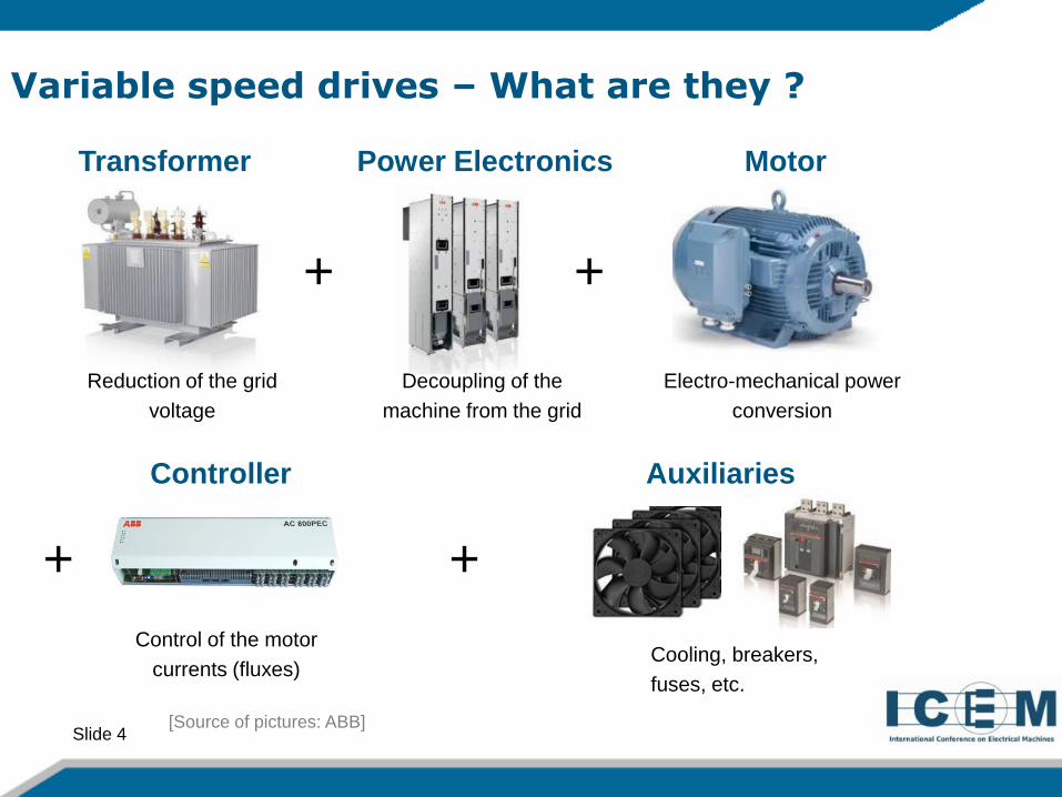
Variable speed drives – What are they ?
+
Transformer
Reduction of the grid
voltage
Power Electronics
+
Motor
Decoupling of the
machine from the grid
Electro-mechanical power
conversion
+
Controller
Control of the motor
currents (fluxes)
+
Auxiliaries
Cooling, breakers,
fuses, etc.
[Source of pictures: ABB]
Slide 5
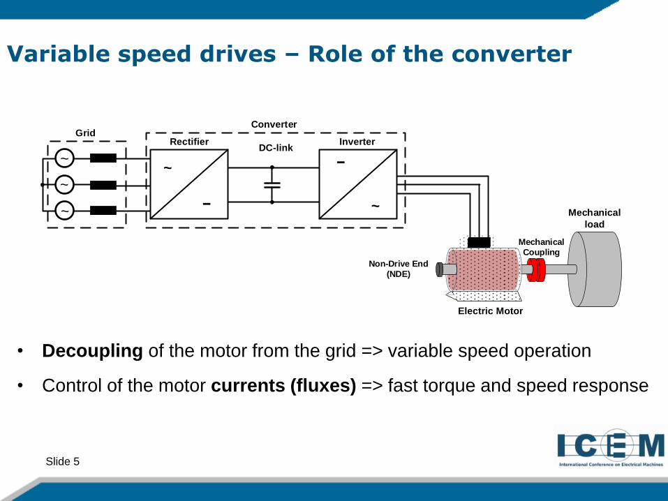
Variable speed drives – Role of the converter
• Decoupling of the motor from the grid => variable speed operation
• Control of the motor currents (fluxes) => fast torque and speed response
Electric Motor
Mechanical
load
Mechanical
Coupling
Non-Drive End
(NDE)
Grid
~
~
~
~
~ −
−
Rectifier InverterDC-link
Converter
Slide 6
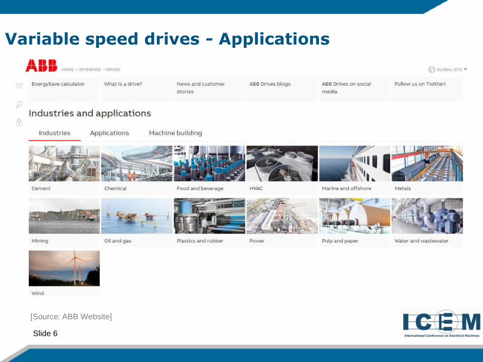
Variable speed drives - Applications
[Source: ABB Website]
Slide 7
Variable Speed Drives
Converter Topologies
Modulation Techniques
Evaluation Criteria and Important System Aspects
Conclusion
Outline
Slide 8
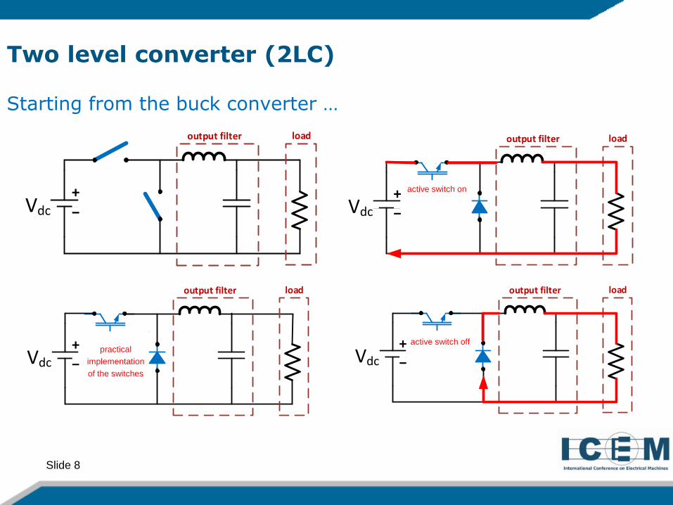
Two level converter (2LC)
Starting from the buck converter …
Vdc
+
−
output filter load
Vdc
+
−
output filter load
Vdc
+
−
output filter load
Vdc
+
−
output filter load
practical
implementation
of the switches
active switch on
active switch off

Slide 9
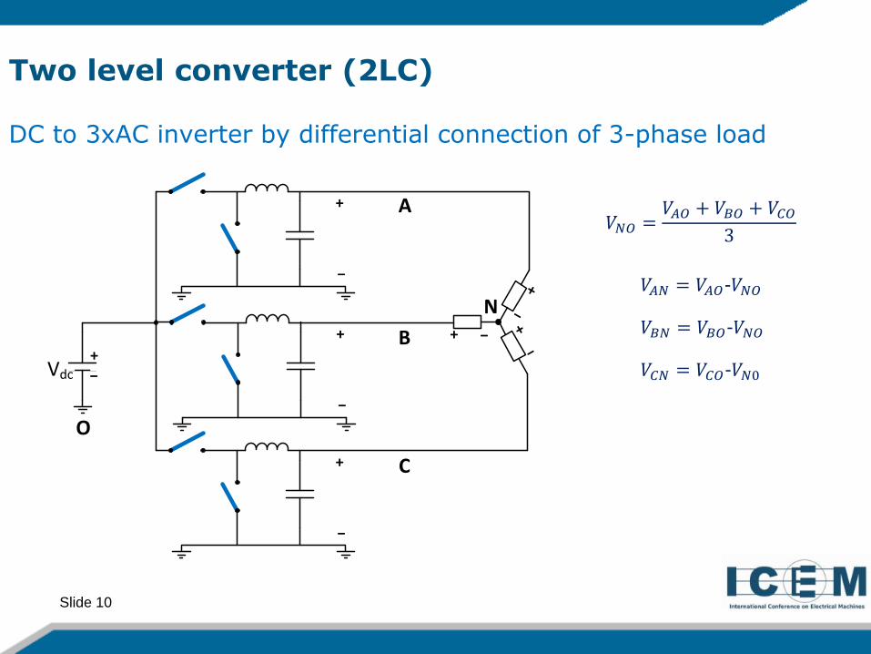
Two level converter (2LC)
DC to 3xAC inverter by differential connection of 3-phase load
A
B
C
+− Vdc
N
+
−
+
−
+
−
+ −
O
Slide 10
Two level converter (2LC)
DC to 3xAC inverter by differential connection of 3-phase load
A
B
C
+− Vdc
N
+
−
+
−
+
−
+ −
O
𝑉𝐴𝑁 = 𝑉𝐴𝑂-𝑉𝑁𝑂
𝑉𝐵𝑁 = 𝑉𝐵𝑂-𝑉𝑁𝑂
𝑉𝐶𝑁 = 𝑉𝐶𝑂-𝑉𝑁0
𝑉𝑁𝑂 =𝑉𝐴𝑂 + 𝑉𝐵𝑂 + 𝑉𝐶𝑂
3

Slide 11
Two level converter (2LC)
DC to 3xAC inverter by differential connection of 3-phase load
A
B
C
+− Vdc N
𝑉𝐴𝑁 = 𝑉𝐴𝑂-𝑉𝑁𝑂
𝑉𝐵𝑁 = 𝑉𝐵𝑂-𝑉𝑁𝑂
𝑉𝐶𝑁 = 𝑉𝐶𝑂-𝑉𝑁0
𝑉𝑁𝑂 =𝑉𝐴𝑂 + 𝑉𝐵𝑂 + 𝑉𝐶𝑂
3
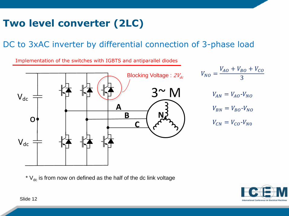
Slide 12
Two level converter (2LC)
DC to 3xAC inverter by differential connection of 3-phase load
3~ M
oA
BC
Vdc
N
Vdc
* Vdc is from now on defined as the half of the dc link voltage
Implementation of the switches with IGBTS and antiparallel diodes
Blocking Voltage : 2Vdc
𝑉𝐴𝑁 = 𝑉𝐴𝑂-𝑉𝑁𝑂
𝑉𝐵𝑁 = 𝑉𝐵𝑂-𝑉𝑁𝑂
𝑉𝐶𝑁 = 𝑉𝐶𝑂-𝑉𝑁0
𝑉𝑁𝑂 =𝑉𝐴𝑂 + 𝑉𝐵𝑂 + 𝑉𝐶𝑂
3
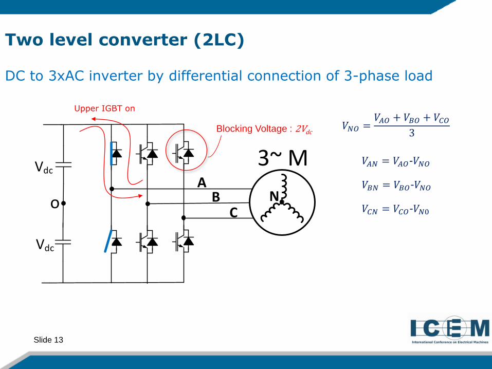
Slide 13
Two level converter (2LC)
DC to 3xAC inverter by differential connection of 3-phase load
Blocking Voltage : 2Vdc
3~ M
oA
BC
N
Vdc
Vdc
𝑉𝐴𝑁 = 𝑉𝐴𝑂-𝑉𝑁𝑂
𝑉𝐵𝑁 = 𝑉𝐵𝑂-𝑉𝑁𝑂
𝑉𝐶𝑁 = 𝑉𝐶𝑂-𝑉𝑁0
𝑉𝑁𝑂 =𝑉𝐴𝑂 + 𝑉𝐵𝑂 + 𝑉𝐶𝑂
3
Upper IGBT on

Slide 14
3~ M
oA
BC
N
Vdc
Vdc
Two level converter (2LC)
DC to 3xAC inverter by differential connection of 3-phase load
Blocking Voltage : 2Vdc
𝑉𝐴𝑁 = 𝑉𝐴𝑂-𝑉𝑁𝑂
𝑉𝐵𝑁 = 𝑉𝐵𝑂-𝑉𝑁𝑂
𝑉𝐶𝑁 = 𝑉𝐶𝑂-𝑉𝑁0
𝑉𝑁𝑂 =𝑉𝐴𝑂 + 𝑉𝐵𝑂 + 𝑉𝐶𝑂
3
Lower IGBT on
Slide 15
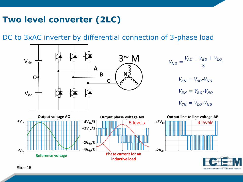
Two level converter (2LC)
DC to 3xAC inverter by differential connection of 3-phase load
𝑉𝐴𝑁 = 𝑉𝐴𝑂-𝑉𝑁𝑂
𝑉𝐵𝑁 = 𝑉𝐵𝑂-𝑉𝑁𝑂
𝑉𝐶𝑁 = 𝑉𝐶𝑂-𝑉𝑁0
𝑉𝑁𝑂 =𝑉𝐴𝑂 + 𝑉𝐵𝑂 + 𝑉𝐶𝑂
3
+Vdc
-Vdc
Output voltage AO Output phase voltage AN Output line to line voltage AB+2Vdc
-2VdcPhase current for an
inductive load
+4Vdc/3
+2Vdc/3
-4Vdc/3
-2Vdc/3
Reference voltage
5 levels 3 levels
3~ M
oA
BC
Vdc
N
Vdc

Slide 16
3-Level Neutral Point Clamped Converter (3LNPC2)
Vdc
Vdc
+
−
+
−
clamping
diodes
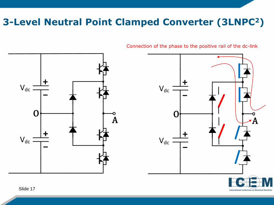
Slide 17
3-Level Neutral Point Clamped Converter (3LNPC2)
Vdc
Vdc
+
−
+
−
+
−
+
−
Vdc
Vdc
AO
AO
Connection of the phase to the positive rail of the dc-link
Slide 18
+
−
+
−
Vdc
Vdc
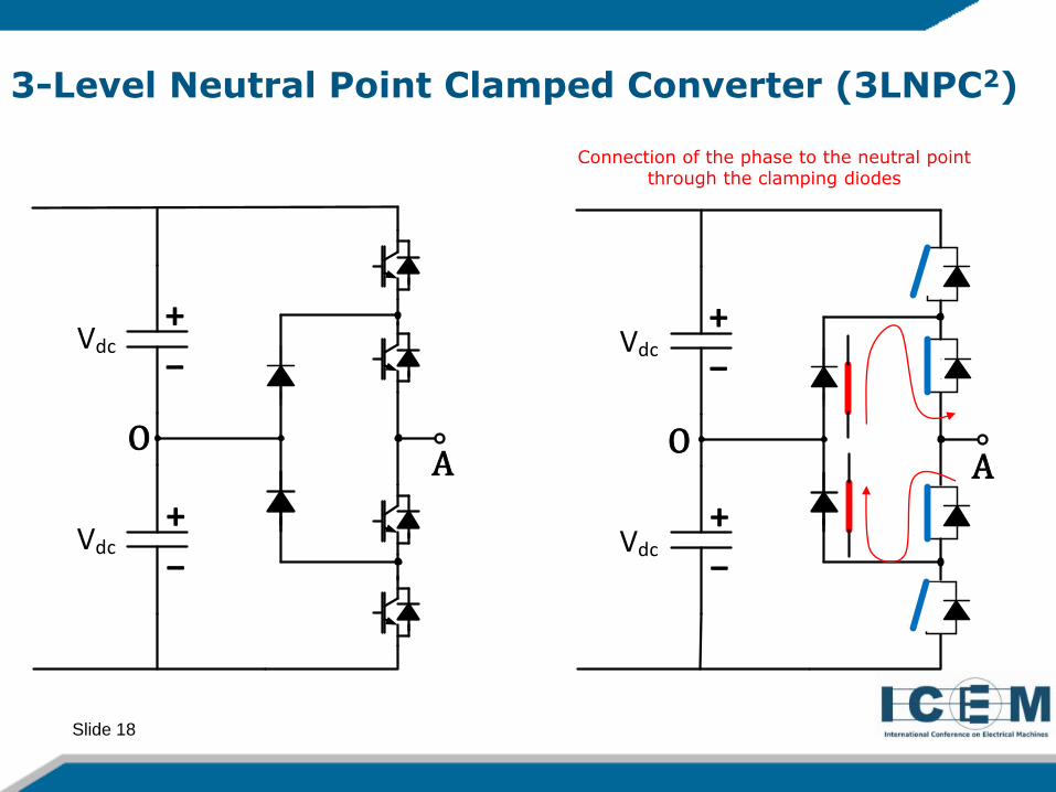
3-Level Neutral Point Clamped Converter (3LNPC2)
Vdc
Vdc
+
−
+
−
AO
AO
Connection of the phase to the neutral point through the clamping diodes
Slide 19
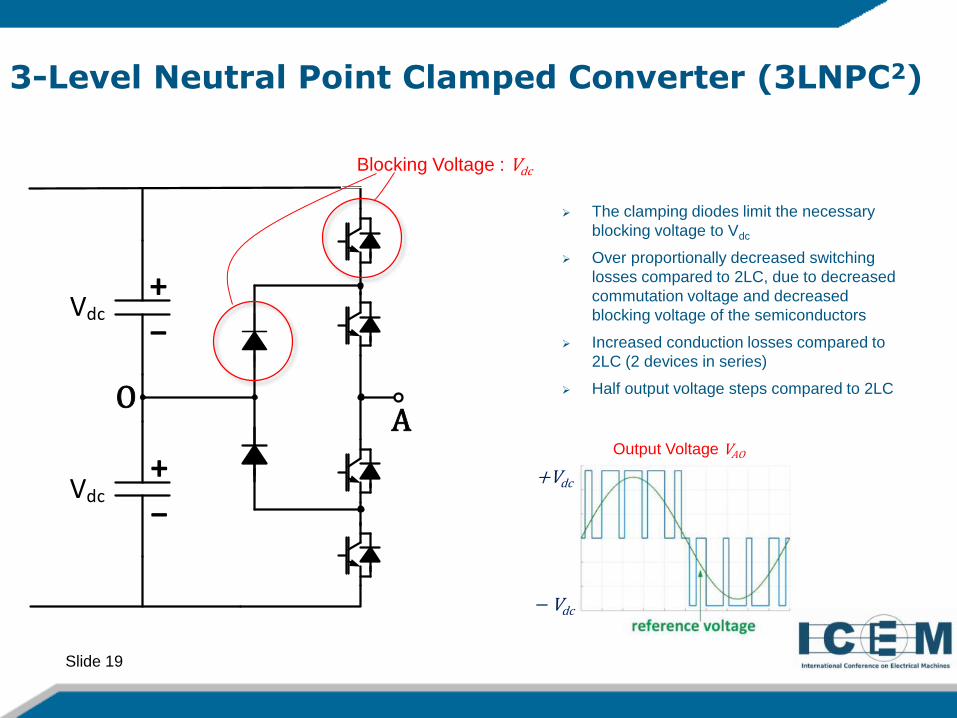
3-Level Neutral Point Clamped Converter (3LNPC2)
The clamping diodes limit the necessary
blocking voltage to Vdc
Over proportionally decreased switching
losses compared to 2LC, due to decreased
commutation voltage and decreased
blocking voltage of the semiconductors
Increased conduction losses compared to
2LC (2 devices in series)
Half output voltage steps compared to 2LC
Vdc
Vdc
+
−
+
−
Blocking Voltage : Vdc
AO
+Vdc
− Vdc
Output Voltage VAO

Slide 20
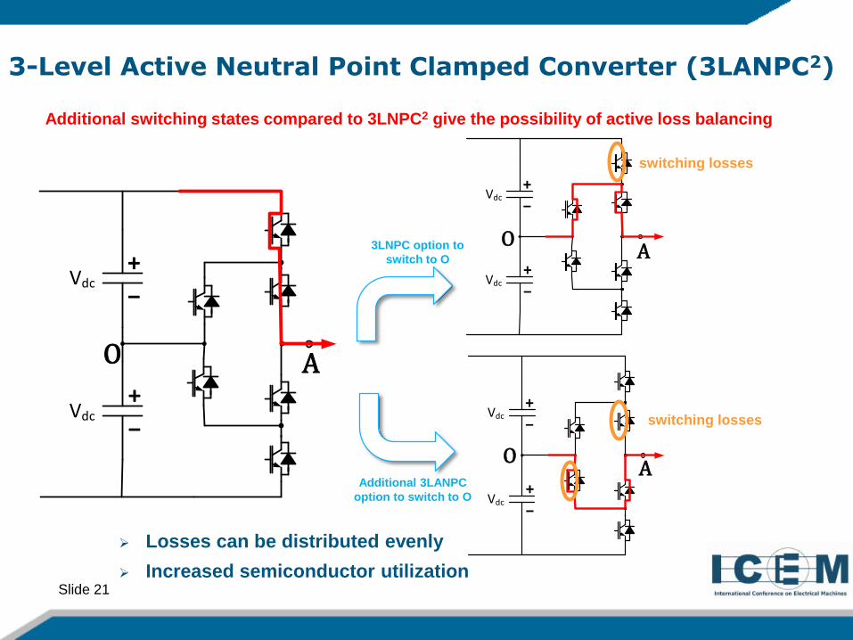
3-Level Active Neutral Point Clamped Converter (3LANPC2)
Vdc
Vdc
+
−
+
−
active
switches
Slide 21
Vdc
Vdc
+
−
+
−
Vdc
Vdc
+
−
+
−
3-Level Active Neutral Point Clamped Converter (3LANPC2)
Additional switching states compared to 3LNPC2 give the possibility of active loss balancing
switching losses
switching losses
Losses can be distributed evenly
Increased semiconductor utilization
Vdc
Vdc
+
−
+
−
3LNPC option to
switch to O
Additional 3LANPC
option to switch to O
O A
OA
OA
Slide 22
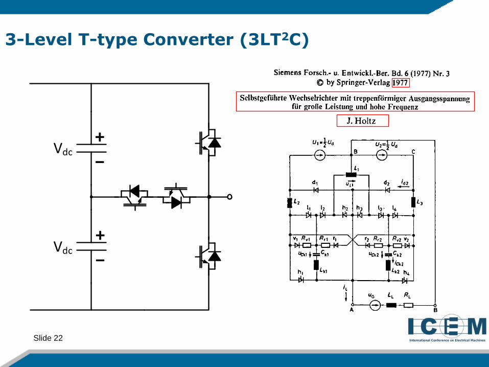
3-Level T-type Converter (3LT2C)
+
−
+
−
Vdc
Vdc

Slide 23
+
−
+
−
Vdc
Vdc
+
−
+
−
Vdc
Vdc
3-Level T-type Converter (3LT2C)
AO
Connection of the phase to the positive rail of the dc-link
AO

Slide 24
3-Level T-type Converter (3LT2C)
Connection of the phase to the neutral point
+
−
+
−
Vdc
Vdc
AO
+
−
+
−
Vdc
Vdc
AO

Slide 25
3-Level T-type Converter (3LT2C)
The conventional 2LC topology is extended
with an active bidirectional switch to the dc-
link neutral point
Due to the reduced blocking voltage the
middle switch has low switching losses and
acceptable conduction losses
Contrary to 3LNPC2 there is no series
connection of devices that have to block the
whole dc-link voltage lower conduction
losses
Half output voltage steps compared to 2LC
+Vdc
− Vdc
Output Voltage VAO
+
−
+
−
Vdc
Vdc
Blocking Voltage : 2Vdc
Blocking Voltage : Vdc
AO
Slide 26
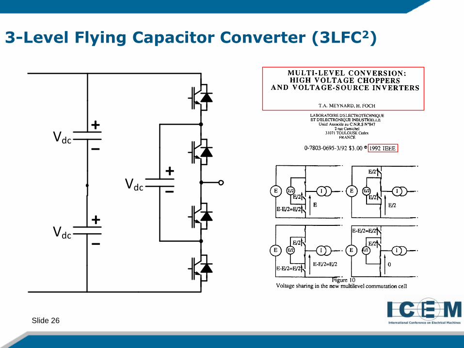
3-Level Flying Capacitor Converter (3LFC2)
+
−
+
−
Vdc
+−
Vdc
Vdc
Slide 27
+
−
+
−
Vdc
+−
Vdc
Vdc
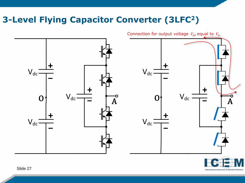
3-Level Flying Capacitor Converter (3LFC2)
AO
Connection for output voltage VAO equal to Vdc
Vdc
Vdc
+
−
+
−
Vdc
+− AO

Slide 28
3-Level Flying Capacitor Converter (3LFC2)
Connection for output voltage VAO equal to zero
+
−
+
−
Vdc
+−
Vdc
Vdc
AO
Vdc
Vdc
+
−
+
−
Vdc
+− AO
Slide 29
+
−
+
−
Vdc
+−
Vdc
Vdc
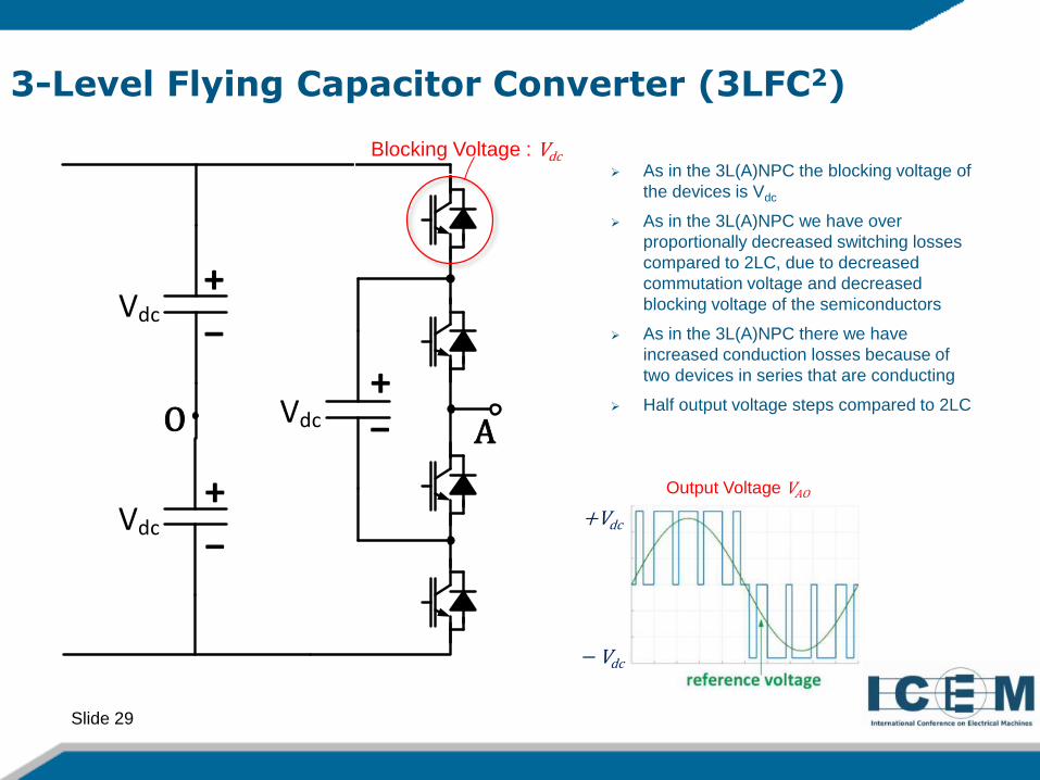
3-Level Flying Capacitor Converter (3LFC2)
Blocking Voltage : Vdc As in the 3L(A)NPC the blocking voltage of
the devices is Vdc
As in the 3L(A)NPC we have over
proportionally decreased switching losses
compared to 2LC, due to decreased
commutation voltage and decreased
blocking voltage of the semiconductors
As in the 3L(A)NPC there we have
increased conduction losses because of
two devices in series that are conducting
Half output voltage steps compared to 2LC
+Vdc
− Vdc
Output Voltage VAO
AO
Slide 30
Variable Speed Drives
Converter Topologies
Modulation Techniques
Evaluation Criteria and Important Drive System Aspects
Conclusion
Outline
Slide 31
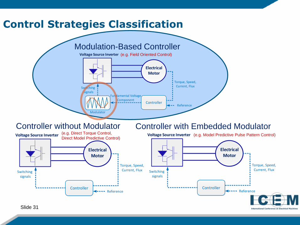
Control Strategies Classification
Voltage Source Inverter
Electrical Motor
Controller
Torque, Speed, Current, Flux
Reference
Switching signals
Fundamental VoltageComponent
Modulator
Modulation-Based Controller
Voltage Source Inverter
Electrical Motor
Controller
Torque, Speed, Current, Flux
Reference
Switching signals
Controller without Modulator
(e.g. Field Oriented Control)
(e.g. Direct Torque Control,
Direct Model Predictive Control)Voltage Source Inverter
Electrical Motor
Controller
Torque, Speed, Current, Flux
Reference
Switching signals
Controller with Embedded Modulator(e.g. Model Predictive Pulse Pattern Control)
Slide 32
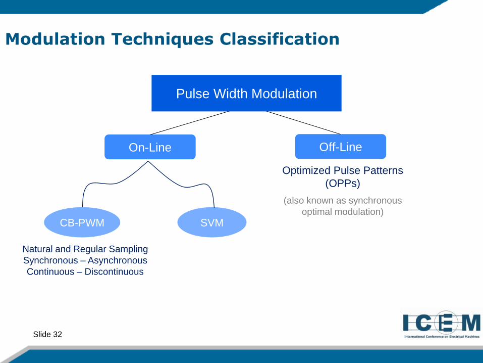
Modulation Techniques Classification
CB-PWM SVM
On-Line
Natural and Regular Sampling
Synchronous – Asynchronous
Continuous – Discontinuous
Off-Line
Pulse Width Modulation
Optimized Pulse Patterns
(OPPs)
(also known as synchronous
optimal modulation)

Slide 33
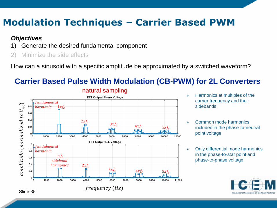
Modulation Techniques – Carrier Based PWM
Objectives
1) Generate the desired fundamental component
2) Minimize the side effects
How can a sinusoid with a specific amplitude be approximated by a switched waveform?
1st approach: Consider only the switching period and calculate the
fundamental component from the volt-second equality
�
𝑇𝑝
𝑣∗𝑑𝑡 = �
𝑡𝑜𝑛
𝑉𝑑𝑐𝑑𝑡 ⇒
𝑇𝑝 � 𝑣∗ 𝑡𝑠 = 𝑡𝑜𝑛 � 𝑉𝑑𝑐 ⇒
𝑣∗ 𝑡𝑠 =𝑡𝑜𝑛
𝑇𝑠� 𝑉𝑑𝑐
time instant of sampling
−𝑉𝑑𝑐
+𝑉𝑑𝑐
𝑣∗ 𝑡
𝑣∗ 𝑡

Slide 34
Modulation Techniques – Carrier Based PWM
Objectives
1) Generate the desired fundamental component
2) Minimize the side effects
How can a sinusoid with a specific amplitude be approximated by a switched waveform?
+𝑉𝑑𝑐
−𝑉𝑑𝑐
𝑣∗ 𝑡
m=�𝑣∗
𝑉𝑑𝑐
𝑚𝑜𝑑𝑢𝑙𝑎𝑡𝑖𝑜𝑛 𝑖𝑛𝑑𝑒𝑥:
Carrier Based Pulse Width Modulation (CB-PWM) for 2L Converters
natural sampling
Slide 35
Modulation Techniques – Carrier Based PWM
Objectives
1) Generate the desired fundamental component
2) Minimize the side effects
How can a sinusoid with a specific amplitude be approximated by a switched waveform?
Carrier Based Pulse Width Modulation (CB-PWM) for 2L Converters
𝑓𝑟𝑒𝑞𝑢𝑒𝑛𝑐𝑦 (𝐻𝑧)
𝑎𝑚
𝑝𝑙𝑖
𝑡𝑢𝑑
𝑒(𝑛
𝑜𝑟𝑚
𝑎𝑙𝑖
𝑧𝑒𝑑
𝑡𝑜𝑉
𝑑𝑐)
𝑓𝑢𝑛𝑑𝑎𝑚𝑒𝑛𝑡𝑎𝑙ℎ𝑎𝑟𝑚𝑜𝑛𝑖𝑐 1𝑥𝑓𝑐
1𝑥𝑓𝑐
𝑠𝑖𝑑𝑒𝑏𝑎𝑛𝑑ℎ𝑎𝑟𝑚𝑜𝑛𝑖𝑐𝑠
2𝑥𝑓𝑐3𝑥𝑓𝑐 4𝑥𝑓𝑐 5𝑥𝑓𝑐
2𝑥𝑓𝑐
3𝑥𝑓𝑐 4𝑥𝑓𝑐 5𝑥𝑓𝑐
𝑓𝑢𝑛𝑑𝑎𝑚𝑒𝑛𝑡𝑎𝑙ℎ𝑎𝑟𝑚𝑜𝑛𝑖𝑐
Harmonics at multiples of the
carrier frequency and their
sidebands
Common mode harmonics
included in the phase-to-neutral
point voltage
Only differential mode harmonics
in the phase-to-star point and
phase-to-phase voltage
natural sampling
Slide 36
Modulation Techniques – Carrier Based PWM
Objectives
1) Generate the desired fundamental component
2) Minimize the side effects
How can a sinusoid with a specific amplitude be approximated by a switched waveform?
Carrier Based Pulse Width Modulation (CB-PWM) for 2L Converters
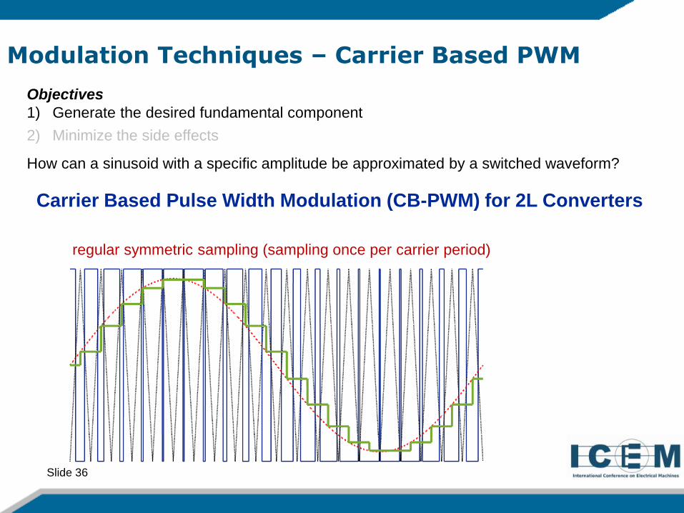
regular symmetric sampling (sampling once per carrier period)
Slide 37
Modulation Techniques – Carrier Based PWM
Objectives
1) Generate the desired fundamental component
2) Minimize the side effects
How can a sinusoid with a specific amplitude be approximated by a switched waveform?
Carrier Based Pulse Width Modulation (CB-PWM) for 2L Converters
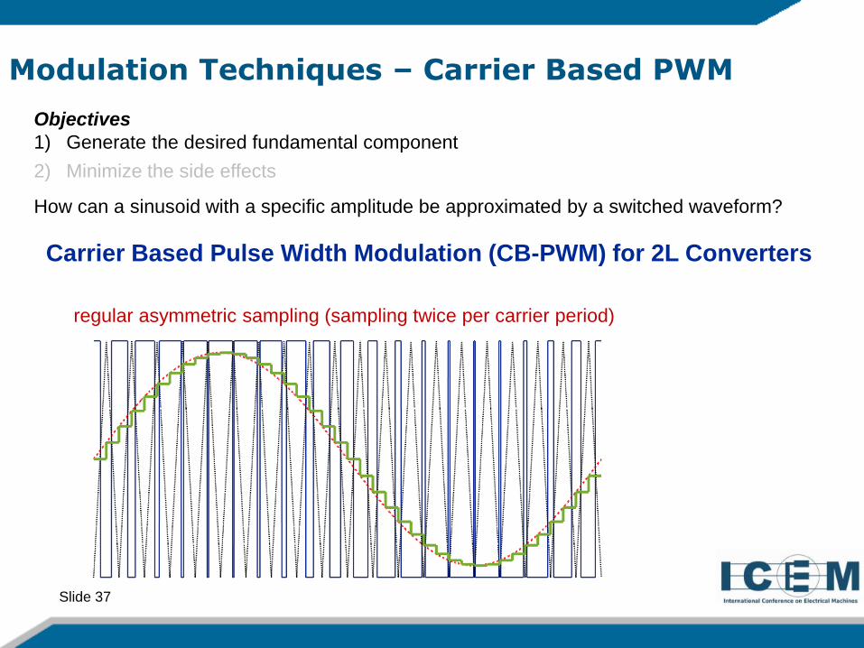
regular asymmetric sampling (sampling twice per carrier period)
Slide 38
Modulation Techniques – Carrier Based PWM
Objectives
1) Generate the desired fundamental component
2) Minimize the side effects
How can a sinusoid with a specific amplitude be approximated by a switched waveform?
Carrier Based Pulse Width Modulation (CB-PWM) for 2L Converters
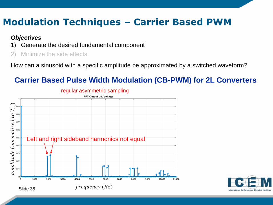
regular asymmetric sampling
𝑓𝑟𝑒𝑞𝑢𝑒𝑛𝑐𝑦 (𝐻𝑧)
𝑎𝑚
𝑝𝑙𝑖
𝑡𝑢𝑑
𝑒(𝑛
𝑜𝑟𝑚
𝑎𝑙𝑖
𝑧𝑒𝑑
𝑡𝑜𝑉
𝑑𝑐)
Left and right sideband harmonics not equal
Slide 39
Modulation Techniques – Carrier Based PWM
Objectives
1) Generate the desired fundamental component
2) Minimize the side effects
How can a sinusoid with a specific amplitude be approximated by a switched waveform?
Carrier Based Pulse Width Modulation (CB-PWM) for 2L Converters
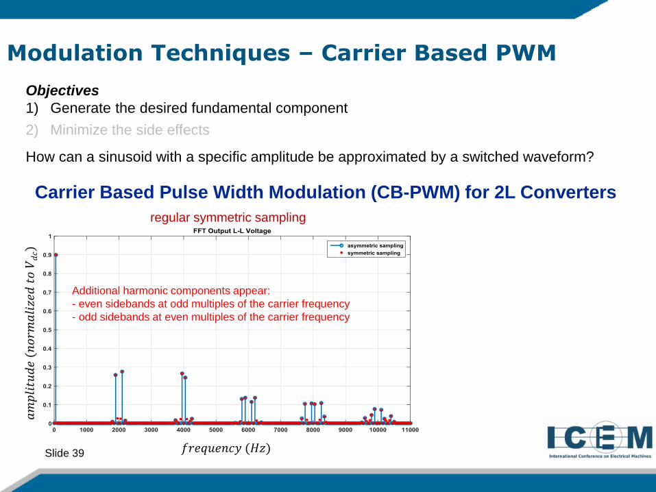
regular symmetric sampling
𝑓𝑟𝑒𝑞𝑢𝑒𝑛𝑐𝑦 (𝐻𝑧)
𝑎𝑚
𝑝𝑙𝑖
𝑡𝑢𝑑
𝑒(𝑛
𝑜𝑟𝑚
𝑎𝑙𝑖
𝑧𝑒𝑑
𝑡𝑜𝑉
𝑑𝑐)
Additional harmonic components appear:
- even sidebands at odd multiples of the carrier frequency
- odd sidebands at even multiples of the carrier frequency

Slide 40
Modulation Techniques – Carrier Based PWM
Objectives
1) Generate the desired fundamental component
2) Minimize the side effects (harmonic current)
o
A
B
CN
~~~
LOAD
If the load star point impedance to the ground is considered
infinite, we have an additional degree of freedom for the
modulation : the Common Mode Voltage (CMV)
Advantages of adding a common mode component:
Increase of the overmodulation limit and thus the inverter
output voltage
Transfer of the harmonic energy to higher frequencies
and thus better filtering and more sinusoidal current for an
inductive load
Addition of a common mode voltage (CMV) to the reference signal
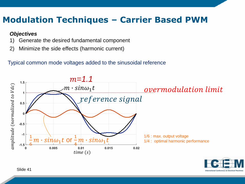
Slide 41
Modulation Techniques – Carrier Based PWM
Objectives
1) Generate the desired fundamental component
2) Minimize the side effects (harmonic current)
𝑚 � 𝑠𝑖𝑛𝜔1𝑡
𝑟𝑒𝑓𝑒𝑟𝑒𝑛𝑐𝑒 𝑠𝑖𝑔𝑛𝑎𝑙
1
6𝑚 � 𝑠𝑖𝑛𝜔1𝑡 or
1
4𝑚 � 𝑠𝑖𝑛𝜔1𝑡
𝑚=1.1
1/6 : max. output voltage
1/4 : optimal harmonic performance
𝑜𝑣𝑒𝑟𝑚𝑜𝑑𝑢𝑙𝑎𝑡𝑖𝑜𝑛 𝑙𝑖𝑚𝑖𝑡
𝑎𝑚
𝑝𝑙𝑖
𝑡𝑢𝑑
𝑒(𝑛
𝑜𝑟𝑚
𝑎𝑙𝑖
𝑧𝑒𝑑
𝑡𝑜𝑉
𝑑𝑐)
𝑡𝑖𝑚𝑒 (𝑠)
Typical common mode voltages added to the sinusoidal reference
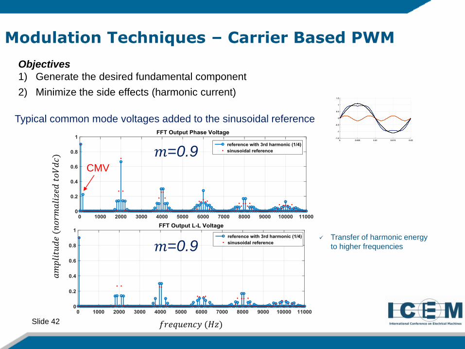
Slide 42
Modulation Techniques – Carrier Based PWM
Objectives
1) Generate the desired fundamental component
2) Minimize the side effects (harmonic current)
Typical common mode voltages added to the sinusoidal reference
𝑓𝑟𝑒𝑞𝑢𝑒𝑛𝑐𝑦 (𝐻𝑧)
𝑎𝑚
𝑝𝑙𝑖
𝑡𝑢𝑑
𝑒(𝑛
𝑜𝑟𝑚
𝑎𝑙𝑖
𝑧𝑒𝑑
𝑡𝑜𝑉
𝑑𝑐)
CMV
𝑚=0.9
𝑚=0.9 Transfer of harmonic energy
to higher frequencies
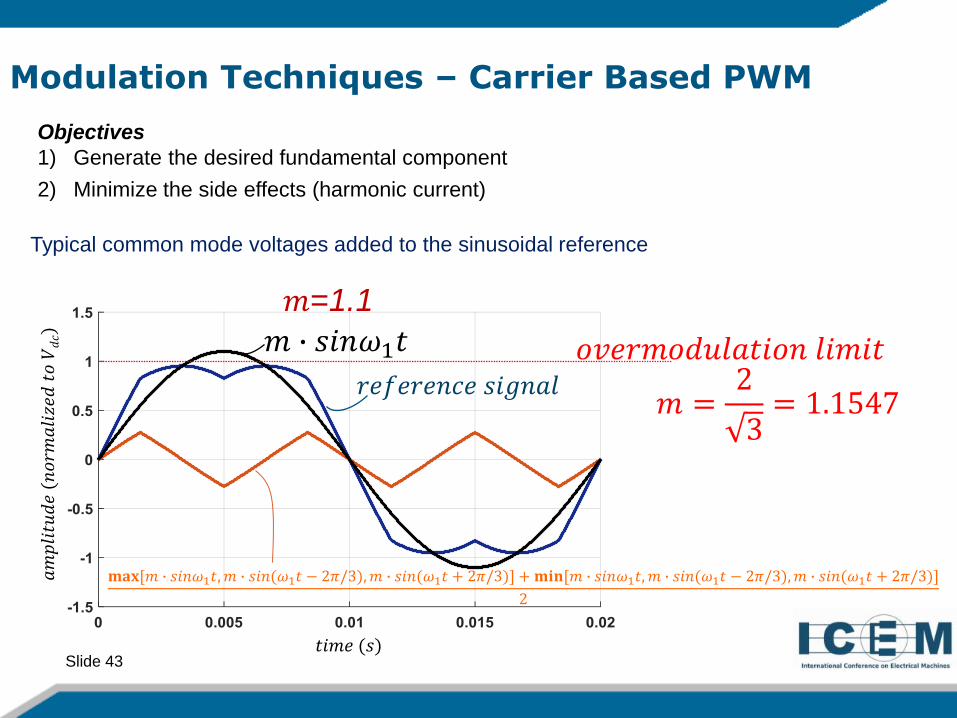
Slide 43
Modulation Techniques – Carrier Based PWM
Objectives
1) Generate the desired fundamental component
2) Minimize the side effects (harmonic current)
Typical common mode voltages added to the sinusoidal reference
𝑚 � 𝑠𝑖𝑛𝜔1𝑡
𝑟𝑒𝑓𝑒𝑟𝑒𝑛𝑐𝑒 𝑠𝑖𝑔𝑛𝑎𝑙
𝐦𝐚𝐱[𝑚 � 𝑠𝑖𝑛𝜔1𝑡, 𝑚 � 𝑠𝑖𝑛(𝜔1𝑡 − 2𝜋/3), 𝑚 � 𝑠𝑖𝑛(𝜔1𝑡 + 2𝜋/3)] + 𝐦𝐢𝐧[𝑚 � 𝑠𝑖𝑛𝜔1𝑡, 𝑚 � 𝑠𝑖𝑛(𝜔1𝑡 − 2𝜋/3), 𝑚 � 𝑠𝑖𝑛(𝜔1𝑡 + 2𝜋/3)]
2
𝑚=1.1
𝑜𝑣𝑒𝑟𝑚𝑜𝑑𝑢𝑙𝑎𝑡𝑖𝑜𝑛 𝑙𝑖𝑚𝑖𝑡
𝑎𝑚
𝑝𝑙𝑖
𝑡𝑢𝑑
𝑒(𝑛
𝑜𝑟𝑚
𝑎𝑙𝑖
𝑧𝑒𝑑
𝑡𝑜𝑉
𝑑𝑐)
𝑡𝑖𝑚𝑒 (𝑠)
𝑚 =2
3= 1.1547

Slide 44
Modulation Techniques – Carrier Based PWM
Objectives
1) Generate the desired fundamental component
2) Minimize the side effects (harmonic current)
Typical common mode voltages added to the sinusoidal reference
𝑎𝑚
𝑝𝑙𝑖
𝑡𝑢𝑑
𝑒(𝑛
𝑜𝑟𝑚
𝑎𝑙𝑖
𝑧𝑒𝑑
𝑡𝑜𝑈
𝑑𝑐)
𝑓𝑟𝑒𝑞𝑢𝑒𝑛𝑐𝑦 (𝐻𝑧)
CMV
𝑚=0.9
𝑚=0.9
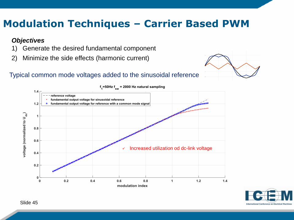
Slide 45
Modulation Techniques – Carrier Based PWM
Objectives
1) Generate the desired fundamental component
2) Minimize the side effects (harmonic current)
Typical common mode voltages added to the sinusoidal reference
Increased utilization od dc-link voltage

Slide 46
Modulation Techniques – Carrier Based PWM
Measurement of the phase current fundamental component
with appropriate sampling only the fundamental current harmonic is measured
fundamental
current harmonic
total current
Slide 47
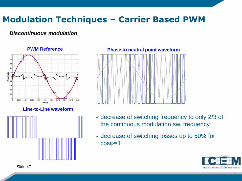
Modulation Techniques – Carrier Based PWM
Discontinuous modulation
PWM Reference Phase to neutral point waveform
Line-to-Line waveform
decrease of switching frequency to only 2/3 of
the continuous modulation sw. frequency
decrease of switching losses up to 50% for
cosφ=1
Slide 48
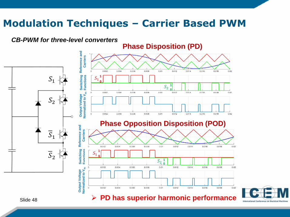
Modulation Techniques – Carrier Based PWM
CB-PWM for three-level converters Phase Disposition (PD)
Phase Opposition Disposition (POD)
𝑆1
𝑆1
𝑆1
𝑆21
0
1
0
𝑆2
𝑆2
Ou
tpu
t V
olt
ag
e
No
rmali
zed
to
Vd
c
Refe
ren
ce a
nd
Carr
iers
Sw
itch
ing
Fu
nc
tio
ns
𝑆1
𝑆210
1
0
Ou
tpu
t V
olt
ag
e
No
rmali
zed
to
Vd
c
Refe
ren
ce a
nd
Carr
iers
Sw
itch
ing
Fu
nc
tio
ns
PD has superior harmonic performance
Slide 49
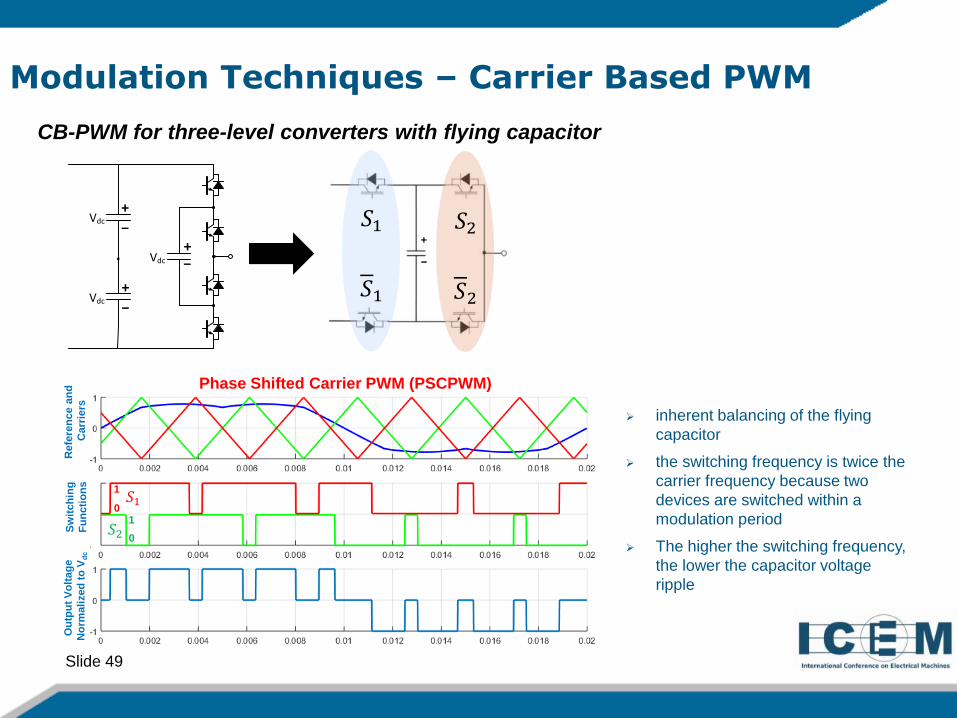
Modulation Techniques – Carrier Based PWM
CB-PWM for three-level converters with flying capacitor
inherent balancing of the flying
capacitor
the switching frequency is twice the
carrier frequency because two
devices are switched within a
modulation period
The higher the switching frequency,
the lower the capacitor voltage
ripple
𝑆1
𝑆1
𝑆2
𝑆2
Phase Shifted Carrier PWM (PSCPWM)
Ou
tpu
t V
olt
ag
e
No
rmali
zed
to
Vd
c
Refe
ren
ce a
nd
Carr
iers
Sw
itch
ing
Fu
nc
tio
ns
𝑆1
𝑆2
+
−
+
−
Vdc
+−
Vdc
Vdc
1
0
1
0
+
−

Slide 50
Modulation Techniques – Optimized Pulse Patterns
Objectives
1) Generate the desired fundamental component
2) Minimize the side effects
How can a sinusoid with a specific amplitude be approximated by a switched waveform?
2nd approach: Consider the fundamental period and calculate the fundamental component from the
Fourier integral
-Vdc
+Vdc
V�𝑣∗ = 𝑉𝑑𝑐 �
2
𝜋�
0
𝜋
𝑓 𝜔𝑡 � sin𝜔1𝑡 � 𝑑𝜔𝑡 ⇒
�𝑣∗ = 𝑉𝑑𝑐 �4
𝜋�
𝑖=1
𝑁
Δu𝑖 � cos𝑎𝑖
N : number of switching angles in a quarter wave
Δu𝑖 : switching function step at switching angle 𝑎𝑖
e.g. for 3-level inverter and quarter wave symmetry
Slide 51
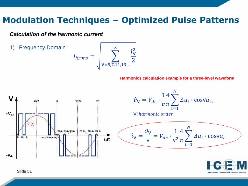
Modulation Techniques – Optimized Pulse Patterns
Calculation of the harmonic current
1) Frequency Domain
𝐼ℎ,𝑟𝑚𝑠 = �
ν=5,7,11,13…
∞𝚤ν2
2
-Vdc
+Vdc
V �𝑣v = 𝑉𝑑𝑐 �1
𝑣
4
𝜋�
𝑖=1
𝑁
𝛥𝑢𝑖 � cosν𝑎𝑖 ,
ν: ℎ𝑎𝑟𝑚𝑜𝑛𝑖𝑐 𝑜𝑟𝑑𝑒𝑟
Harmonics calculation example for a three-level waveform
𝚤ν =�𝑣ν
ν= 𝑉𝑑𝑐 �
1
ν2
4
𝜋�
𝑖=1
𝑁
𝛥𝑢𝑖 � cosν𝑎𝑖
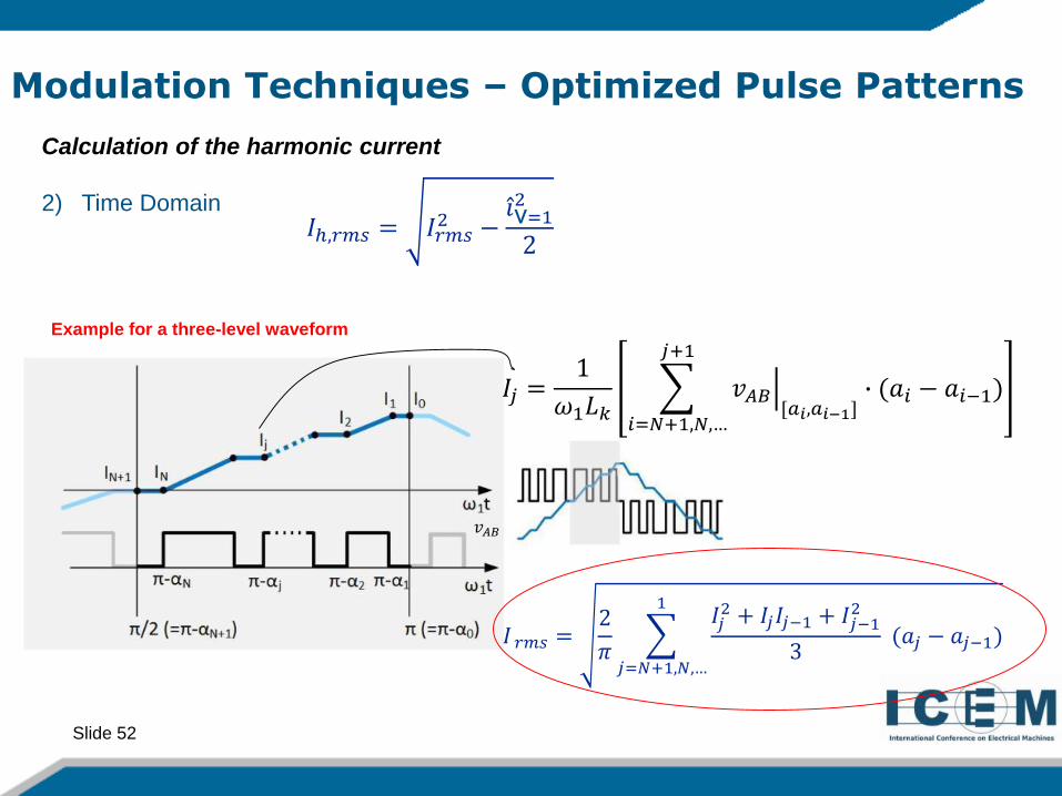
Slide 52
Modulation Techniques – Optimized Pulse Patterns
Calculation of the harmonic current
2) Time Domain𝐼ℎ,𝑟𝑚𝑠 = 𝐼𝑟𝑚𝑠
2 −𝚤ν=12
2
Example for a three-level waveform
𝐼𝑗 =1
𝜔1𝐿𝑘�
𝑖=𝑁+1,𝑁,…
𝑗+1
�𝑣𝐴𝐵[𝑎𝑖,𝑎𝑖−1]
� (𝑎𝑖 − 𝑎𝑖−1)
𝐼 𝑟𝑚𝑠 =2
𝜋�
𝑗=𝑁+1,𝑁,…
1𝐼𝑗
2 + 𝐼𝑗𝐼𝑗−1 + 𝐼𝑗−12
3(𝑎𝑗 − 𝑎𝑗−1)
𝑣𝐴𝐵

Slide 53
Modulation Techniques – Optimized Pulse Patterns
Objectives
1) Generate the desired fundamental component
2) Minimize the side effects
Different optimization criteria (cost functions) can be considered:
- harmonic current
- harmonic motor losses
- motor noise
- common mode voltage
- converter switching losses
Multi-objective optimization also possible
f(α)
α2(0)
α1(0)0 10 20 30 40 50 60 70 80 90
0
9080
7060
5040
30
10
0
2
4
6
10
8
x10-4
20
non-convex cost functions with many local minima!

Slide 54
Optimized Pulse Patterns
Example: 2L waveform when having only 2 switching angles in the range 0-π/2
π/2 π 3π/2 2π
α1 α2 π-α2 π-α1 π+α1 2π-α1 π+α2
ω1t
-Vdc
+Vdc
V
2π-α2
� 𝒊𝝂𝟐
�𝑢𝑣 = 𝑈𝑑𝑐 �1
𝑣
4
𝜋1 + 2 �
𝑖=1
2
𝛥𝑢𝑖 � 𝑐𝑜𝑠𝑣𝑎𝑖 ,
𝑣: ℎ𝑎𝑟𝑚𝑜𝑛𝑖𝑐 𝑜𝑟𝑑𝑒𝑟
��𝑣 =�𝑢𝑣
𝑣= 𝑈𝑑𝑐 �
1
𝑣2
4
𝜋1 + 2 �
𝑖=1
2
𝛥𝑢𝑖 � 𝑐𝑜𝑠𝑣𝑎𝑖
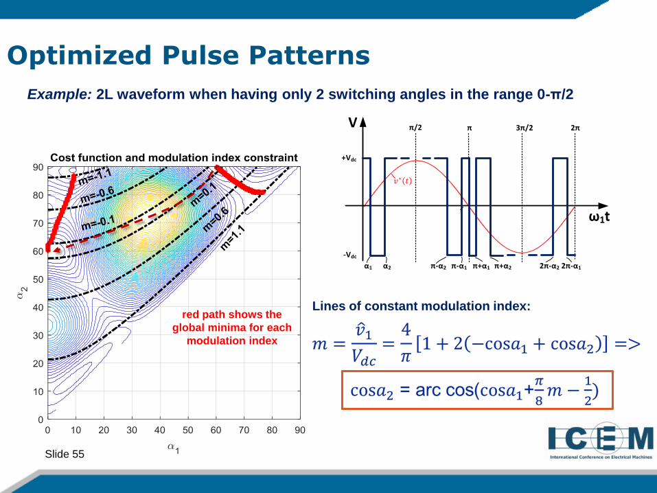
Slide 55
Optimized Pulse Patterns
Example: 2L waveform when having only 2 switching angles in the range 0-π/2
π/2 π 3π/2 2π
α1 α2 π-α2 π-α1 π+α1 2π-α1 π+α2
ω1t
-Vdc
+Vdc
V
2π-α2
red path shows the
global minima for each
modulation index
Lines of constant modulation index:
Slide 56
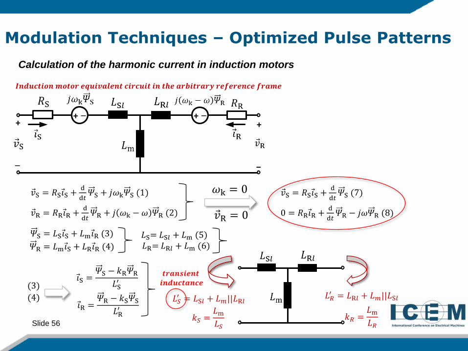
Modulation Techniques – Optimized Pulse Patterns
Calculation of the harmonic current in induction motors
��S = 𝑅S𝚤S +d
d𝑡𝛹S + 𝑗𝜔k𝛹S (1)
��R = 𝑅R𝚤R +d
d𝑡𝛹R + 𝑗 𝜔k − 𝜔 𝛹R (2)
𝛹S = 𝐿S𝚤S + 𝐿m𝚤R (3)
𝛹R = 𝐿m𝚤S + 𝐿R𝚤R (4)
𝑰𝒏𝒅𝒖𝒄𝒕𝒊𝒐𝒏 𝒎𝒐𝒕𝒐𝒓 𝒆𝒒𝒖𝒊𝒗𝒂𝒍𝒆𝒏𝒕 𝒄𝒊𝒓𝒄𝒖𝒊𝒕 𝒊𝒏 𝒕𝒉𝒆 𝒂𝒓𝒃𝒊𝒕𝒓𝒂𝒓𝒚 𝒓𝒆𝒇𝒆𝒓𝒆𝒏𝒄𝒆 𝒇𝒓𝒂𝒎𝒆
𝐿S= 𝐿S𝑙 + 𝐿m (5)𝐿R= 𝐿R𝑙 + 𝐿m (6)
𝚤S =𝛹S − 𝑘R𝛹R
𝐿S′
𝐿𝑆′ = 𝐿S𝑙 + 𝐿𝑚||𝐿R𝑙
(3)
(4)𝚤R =
𝛹R − 𝑘S𝛹S
𝐿R′
𝐿𝑅′ = 𝐿R𝑙 + 𝐿𝑚||𝐿S𝑙
𝑘𝑆 =𝐿m
𝐿𝑆
𝑘𝑅 =𝐿m
𝐿𝑅
𝒕𝒓𝒂𝒏𝒔𝒊𝒆𝒏𝒕𝒊𝒏𝒅𝒖𝒄𝒕𝒂𝒏𝒄𝒆
𝜔k = 0
��R = 0
��S = 𝑅S𝚤S +d
d𝑡𝛹S (7)
0 = 𝑅R𝚤R +d
d𝑡𝛹R − 𝑗𝜔𝛹R (8)
+ ─+
─
+
−
+ ─
Slide 57
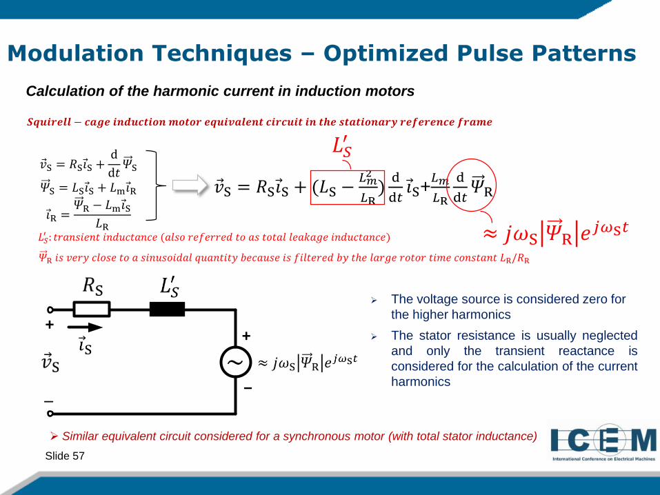
Modulation Techniques – Optimized Pulse Patterns
Calculation of the harmonic current in induction motors
��S = 𝑅S𝚤S +d
d𝑡𝛹S
𝛹S = 𝐿S𝚤S + 𝐿m𝚤R
𝚤R =𝛹R − 𝐿m𝚤S
𝐿R
𝑺𝒒𝒖𝒊𝒓𝒆𝒍𝒍 − 𝒄𝒂𝒈𝒆 𝒊𝒏𝒅𝒖𝒄𝒕𝒊𝒐𝒏 𝒎𝒐𝒕𝒐𝒓 𝒆𝒒𝒖𝒊𝒗𝒂𝒍𝒆𝒏𝒕 𝒄𝒊𝒓𝒄𝒖𝒊𝒕 𝒊𝒏 𝒕𝒉𝒆 𝒔𝒕𝒂𝒕𝒊𝒐𝒏𝒂𝒓𝒚 𝒓𝒆𝒇𝒆𝒓𝒆𝒏𝒄𝒆 𝒇𝒓𝒂𝒎𝒆
��S = 𝑅S𝚤S + (𝐿S −𝐿𝑚
2
𝐿R)
d
d𝑡𝚤S+
𝐿𝑚
𝐿R
d
d𝑡𝛹R
𝐿𝑆′
≈ 𝑗𝜔S 𝛹R 𝑒𝑗𝜔S𝑡𝐿𝑆
′ : 𝑡𝑟𝑎𝑛𝑠𝑖𝑒𝑛𝑡 𝑖𝑛𝑑𝑢𝑐𝑡𝑎𝑛𝑐𝑒 (𝑎𝑙𝑠𝑜 𝑟𝑒𝑓𝑒𝑟𝑟𝑒𝑑 𝑡𝑜 𝑎𝑠 𝑡𝑜𝑡𝑎𝑙 𝑙𝑒𝑎𝑘𝑎𝑔𝑒 𝑖𝑛𝑑𝑢𝑐𝑡𝑎𝑛𝑐𝑒)
𝛹R 𝑖𝑠 𝑣𝑒𝑟𝑦 𝑐𝑙𝑜𝑠𝑒 𝑡𝑜 𝑎 𝑠𝑖𝑛𝑢𝑠𝑜𝑖𝑑𝑎𝑙 𝑞𝑢𝑎𝑛𝑡𝑖𝑡𝑦 𝑏𝑒𝑐𝑎𝑢𝑠𝑒 𝑖𝑠 𝑓𝑖𝑙𝑡𝑒𝑟𝑒𝑑 𝑏𝑦 𝑡ℎ𝑒 𝑙𝑎𝑟𝑔𝑒 𝑟𝑜𝑡𝑜𝑟 𝑡𝑖𝑚𝑒 𝑐𝑜𝑛𝑠𝑡𝑎𝑛𝑡 𝐿R/𝑅R
The voltage source is considered zero for
the higher harmonics
The stator resistance is usually neglected
and only the transient reactance is
considered for the calculation of the current
harmonics
++
─−
Similar equivalent circuit considered for a synchronous motor (with total stator inductance)
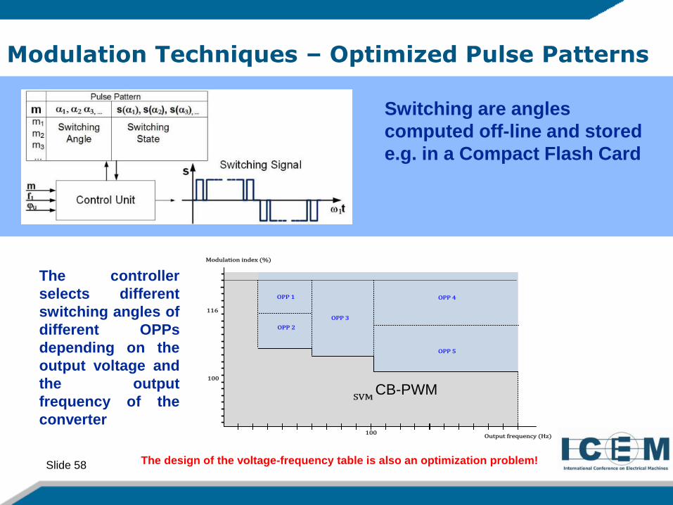
Slide 58
Modulation Techniques – Optimized Pulse Patterns
Switching are angles
computed off-line and stored
e.g. in a Compact Flash Card
The controller
selects different
switching angles of
different OPPs
depending on the
output voltage and
the output
frequency of the
converter
102,3 %
116
100
SVM
OPP 1
Modulation index (%)
Output frequency (Hz)
OPP 2
OPP 3
OPP 4
OPP 5
100
CB-PWM
The design of the voltage-frequency table is also an optimization problem!
Slide 59
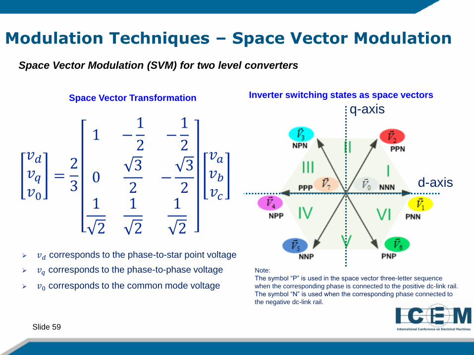
Modulation Techniques – Space Vector Modulation
Space Vector Modulation (SVM) for two level converters
Space Vector Transformation
𝑣𝑑
𝑣𝑞
𝑣0
=2
3
1 −1
2−
1
2
03
2−
3
21
2
1
2
1
2
𝑣𝑎
𝑣𝑏
𝑣𝑐
𝑣𝑑 corresponds to the phase-to-star point voltage
𝑣𝑞 corresponds to the phase-to-phase voltage
𝑣0 corresponds to the common mode voltage
Inverter switching states as space vectors
q-axis
d-axis
Note:
The symbol “P” is used in the space vector three-letter sequence
when the corresponding phase is connected to the positive dc-link rail.
The symbol “N” is used when the corresponding phase connected to
the negative dc-link rail.
Slide 60
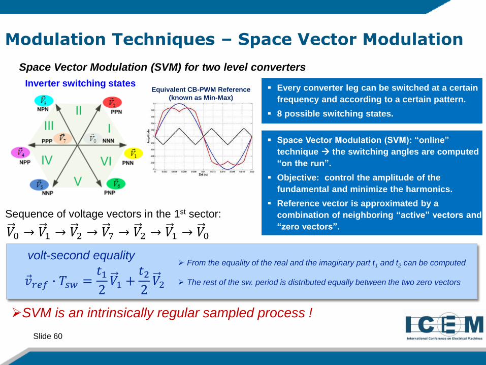
Modulation Techniques – Space Vector Modulation
Space Vector Modulation (SVM) for two level converters
Inverter switching states
Sequence of voltage vectors in the 1st sector:
Every converter leg can be switched at a certain
frequency and according to a certain pattern.
8 possible switching states.
Space Vector Modulation (SVM): “online”
technique the switching angles are computed
“on the run”.
Objective: control the amplitude of the
fundamental and minimize the harmonics.
Reference vector is approximated by a
combination of neighboring “active” vectors and
“zero vectors”.
Equivalent CB-PWM Reference
(known as Min-Max)
��𝑟𝑒𝑓 � 𝑇𝑠𝑤 =𝑡1
2𝑉1 +
𝑡2
2𝑉2
volt-second equality From the equality of the real and the imaginary part t1 and t2 can be computed
The rest of the sw. period is distributed equally between the two zero vectors
𝑉0 → 𝑉1 → 𝑉2 → 𝑉7 → 𝑉2 → 𝑉1 → 𝑉0
SVM is an intrinsically regular sampled process !
Slide 61
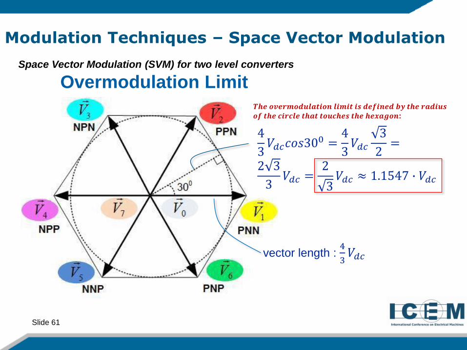
Modulation Techniques – Space Vector Modulation
Space Vector Modulation (SVM) for two level converters
Overmodulation Limit
vector length : 4
3𝑉𝑑𝑐
4
3𝑉𝑑𝑐𝑐𝑜𝑠300 =
4
3𝑉𝑑𝑐
3
2=
2 3
3𝑉𝑑𝑐 =
2
3𝑉𝑑𝑐 ≈ 1.1547 � 𝑉𝑑𝑐
𝑻𝒉𝒆 𝒐𝒗𝒆𝒓𝒎𝒐𝒅𝒖𝒍𝒂𝒕𝒊𝒐𝒏 𝒍𝒊𝒎𝒊𝒕 𝒊𝒔 𝒅𝒆𝒇𝒊𝒏𝒆𝒅 𝒃𝒚 𝒕𝒉𝒆 𝒓𝒂𝒅𝒊𝒖𝒔𝒐𝒇 𝒕𝒉𝒆 𝒄𝒊𝒓𝒄𝒍𝒆 𝒕𝒉𝒂𝒕 𝒕𝒐𝒖𝒄𝒉𝒆𝒔 𝒕𝒉𝒆 𝒉𝒆𝒙𝒂𝒈𝒐𝒏:

Slide 62
Modulation Techniques – Space Vector Modulation
Discontinuous Space Vector Modulation (SVM) for 2L Converters
01277210 >>>>>>> VVVVVVVV
DPWM1 (600 disc.) DPWM3 (300 disc.) Generalized Discontinuous SVM
PWM Reference PWM Reference
Only one zero vector is applied per
switching period
Slide 63
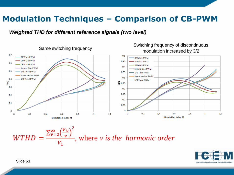
Modulation Techniques – Comparison of CB-PWM
Weighted THD for different reference signals (two level)
Same switching frequencySwitching frequency of discontinuous
modulation increased by 3/2
𝑊𝑇𝐻𝐷 =∑𝜈=2
∞ 𝑉𝜈𝜈
2
𝑉1, where ν is the harmonic order
Slide 64
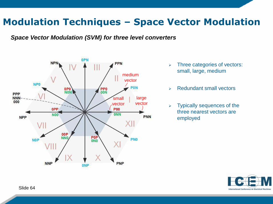
Modulation Techniques – Space Vector Modulation
Space Vector Modulation (SVM) for three level converters
Three categories of vectors:
small, large, medium
Redundant small vectors
Typically sequences of the
three nearest vectors are
employed
large
vector
medium
vector
small
vector
Slide 65
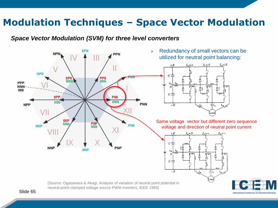
Modulation Techniques – Space Vector Modulation
Space Vector Modulation (SVM) for three level converters
Same voltage vector but different zero sequence
voltage and direction of neutral point current
[Source: Ogasawara & Akagi, Analysis of variation of neutral point potential in
neutral-point-clamped voltage source PWM inverters, IEEE 1993]
Redundancy of small vectors can be
utilized for neutral point balancing:
Slide 66
Modulation Techniques – Summary
Characteristics of the CB-PWM/SVM
Constant switching frequency (can be varied if necessary, e.g. wobbling, but it
is not an inherent characteristic)
Asynchronous modulation
Higher harmonics with frequencies k·fc ± l·f1 , where k, l positive integers
Change of the switching frequency during operation can be easily made
Simple computation of the fundamental harmonic for control purposes
Fast dynamic response with classic PI controllers
Overmodulation is possible at the expense of higher harmonic content, non-
linearity of the output voltage, higher complexity in the calculation of the
fundamental harmonic
Slide 67
Modulation Techniques – Summary
Characteristics of the discontinuous CB-PWM/SVM
Similar characteristics to continuous SVM
There is no switching in one phase for 60° (or 120°in some versions)
The average switching frequency reduces to 2/3 compared to normal SVM
For certain combinations of reference signals and cosφ the switching losses
reduce to only 50% (e.g. DPWM1 and cosφ=1)
Increase of the harmonic content, motor losses, motor temperature rise for the
same carrier frequency
Better harmonic performance than continuous CB-PWM for high modulation
indices if the carrier frequency is increased in order to have the same average
switching frequency
Closer to linearity than normal SVM in the overmodulation region
Slide 68
Modulation Techniques – Summary
Characteristics of the OPPs
Synchronous modulation
Harmonics with frequencies n·f1
Switching frequency proportional to output frequency
Change of the switching frequency during operation requires storage of
additional OPPs
Calculation of the optimal switching angles becomes very time consuming for
high pulse number (ratio of switching to fundamental frequency)

Slide 69
Modulation Techniques – Summary
Characteristics of the OPPs
The computation of the fundamental harmonic is not an easy task as in
SVM/CB-PWM
Transition between OPPs is not trivial
Slow dynamic response compared to SVM when classic PI controllers are
employed
Fast dynamic response only when non-linear controllers are employed (e.g.
MP3C)
Linear relationship of modulation index and output voltage in the
overmodulation region
Increased converter output voltage and low harmonic content at the same time
possible
Slide 70
Variable Speed Drives
Converter Topologies
Modulation Techniques
Evaluation Criteria and Important Drive System Aspects
Conclusion
Outline

Slide 71
Modulation Techniques – Evaluation criteria
Typical evaluation criteria
Dynamic performance of closed-loop control
Converter switching losses versus harmonic current
Overmodulation characteristics
Neutral point / flying capacitor voltage ripple for 3LNPC (and T-Type) / 3LFC converters
Complexity of dynamic balancing for neutral point or flying capacitor voltage
Additional important drive system aspects
Converter and motor losses
Motor electromagnetic noise
Common mode voltage

Slide 72
Drive System Losses
EN 50598-2 : Losses distribution for a 400 kW reference Power Drive System (PDS)
The motor harmonic losses and the converter switching losses are directly influenced by the modulation
Slide 73
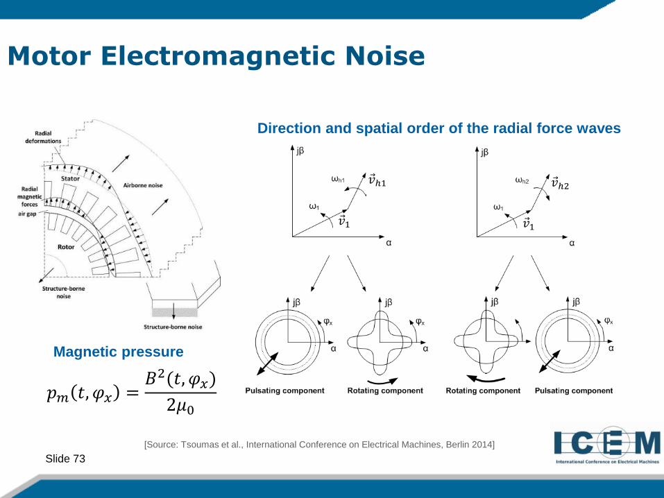
Motor Electromagnetic Noise
[Source: Tsoumas et al., International Conference on Electrical Machines, Berlin 2014]
Direction and spatial order of the radial force waves
𝑝𝑚 𝑡, 𝜑𝑥 =𝐵2(𝑡, 𝜑𝑥)
2𝜇0
Magnetic pressure
��1
��ℎ1 ��ℎ2
��1

Slide 74
Motor Electromagnetic Noise
[Source: Tsoumas et al., International Conference on Electrical Machines, 2014]
Frequencies of the dominating voltage harmonics in SVM
and of the corresponding radial force waves
𝑝𝑚 𝑡, 𝜑𝑥 =𝐵2(𝑡, 𝜑𝑥)
2𝜇0
Magnetic pressure
𝑉(f)
𝑃(f)

Slide 75
Motor Electromagnetic NoiseMeasured Sound Pressure Level
[Source: Tsoumas et al., IEEE Transactions on Industry Applications, 2014]
Randomized SVM does not reduce the noise level even if it sounds better!
Increase of the switching frequency doesn’t always decrease the noise
level, because additional strong vibration modes may be excited
Slide 76
Motor Electromagnetic Noise
[Source: Tsoumas et al., IEEE Transactions on Industry Applications, 2014]
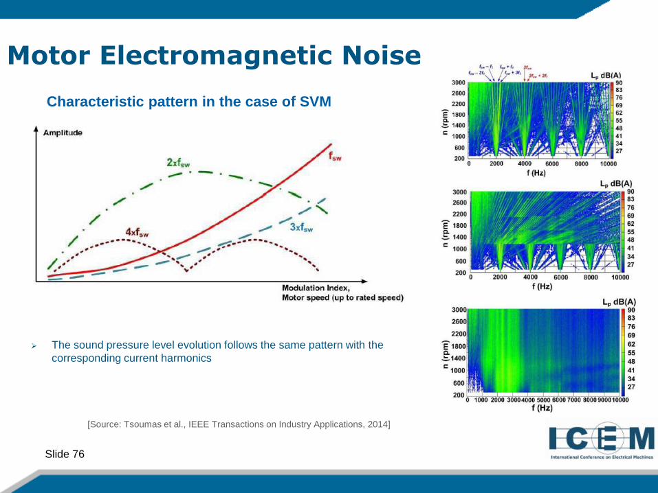
The sound pressure level evolution follows the same pattern with the
corresponding current harmonics
Characteristic pattern in the case of SVM

Slide 77
Common mode voltage
The neutral-to-ground impedance is not infinite
The ground leakage current that will flow through
this impedance depends on the common mode
voltage and the system grounding
The common mode voltage (or part of it) will
appear through a capacitive voltage divider on the
bearings and cause electric discharges.
Slide 78
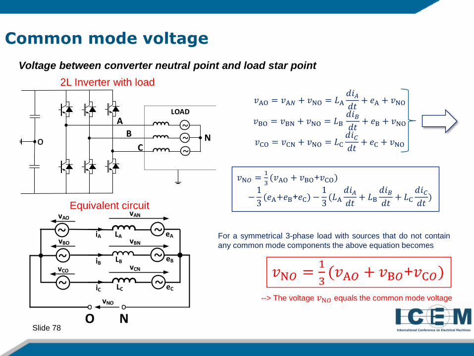
Common mode voltage
Voltage between converter neutral point and load star point
2L Inverter with load
𝑣AO = 𝑣A𝑁 + 𝑣NO = 𝐿A
𝑑𝑖𝐴
𝑑𝑡+ 𝑒A + 𝑣NO
𝑣BO = 𝑣BN + 𝑣NO = 𝐿B
𝑑𝑖𝐵
𝑑𝑡+ 𝑒B + 𝑣NO
𝑣CO = 𝑣CN + 𝑣NO = 𝐿C
𝑑𝑖𝐶
𝑑𝑡+ 𝑒C + 𝑣NO
𝑣N𝑂 =1
3(𝑣AO + 𝑣BO+𝑣CO)
−1
3(𝑒A+𝑒B+𝑒C) −
1
3(𝐿A
𝑑𝑖𝐴
𝑑𝑡+ 𝐿B
𝑑𝑖𝐵
𝑑𝑡+ 𝐿C
𝑑𝑖𝐶
𝑑𝑡)
For a symmetrical 3-phase load with sources that do not contain
any common mode components the above equation becomes
𝑣N𝑂 =1
3(𝑣A𝑂 + 𝑣B𝑂+𝑣C𝑂)
Equivalent circuit
--> The voltage 𝑣N𝑂 equals the common mode voltage
o
A
B
CN
~~~
LOAD
N
~
~
~
~
~
~
O
vNO
vAO
vBO
vCO
iA
iB
iC
vAN
vBN
vCN
eA
eB
eC
LA
LB
LC
Slide 79
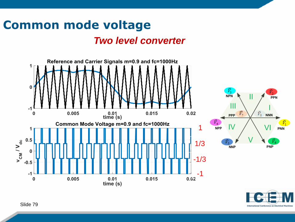
Common mode voltage
Two level converter
1
1/3
-1/3
-1
Slide 80
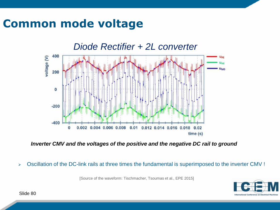
Common mode voltage
[Source of the waveform: Tischmacher, Tsoumas et al., EPE 2015]
Diode Rectifier + 2L converter
Inverter CMV and the voltages of the positive and the negative DC rail to ground
Oscillation of the DC-link rails at three times the fundamental is superimposed to the inverter CMV !
Slide 81
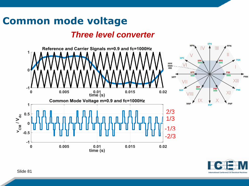
Common mode voltage
Three level converter
2/31/3
-1/3
-2/3
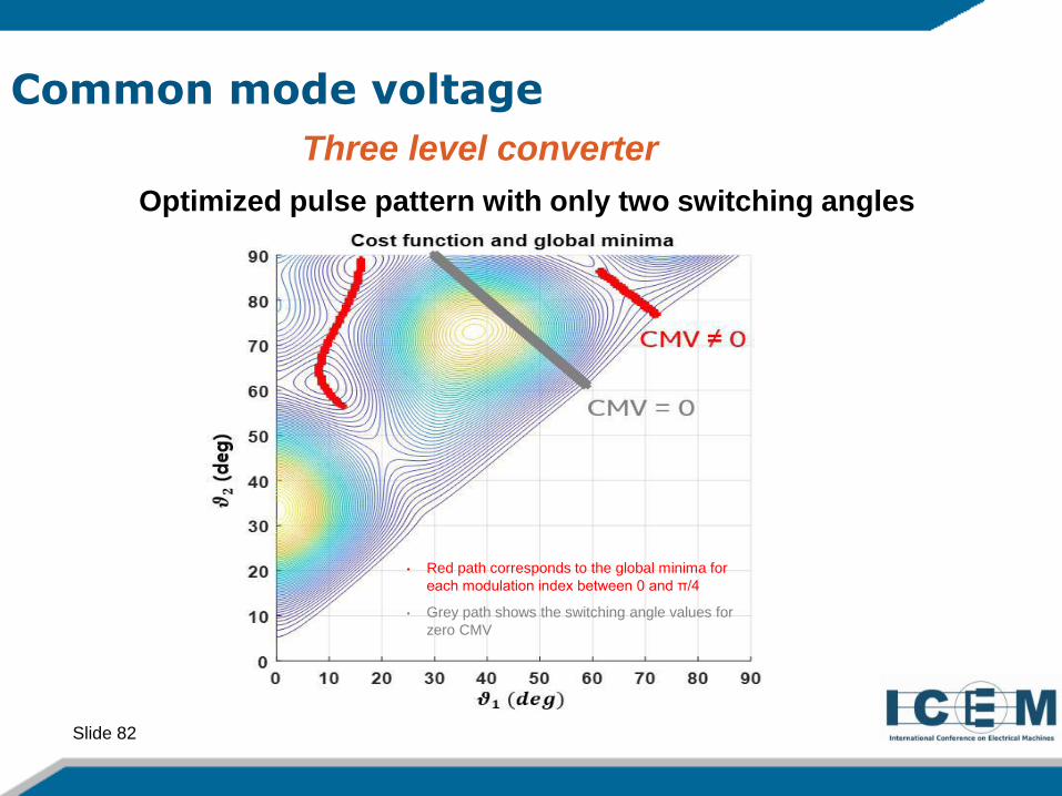
Slide 82
Common mode voltage
Three level converter
Optimized pulse pattern with only two switching angles
• Red path corresponds to the global minima for
each modulation index between 0 and π/4
• Grey path shows the switching angle values for
zero CMV

Slide 83
Common mode voltage
Three level converter
Optimized pulse pattern with only two switching angles
Significant increase of harmonic current
Decrease of maximum possible modulation index
𝑇𝐷𝐷 =∑𝜈=2
∞ 𝐼𝜈2
𝐼1𝑁,
where ν is the harmonic order

Slide 84
Common mode voltage
Motor high frequency equivalent circuit
Bearing Voltage Ratio (BVR) :𝑈𝑏
𝑈𝑁0=
𝐶𝑤𝑟
𝐶𝑤𝑟+𝐶𝑟𝑓+2𝐶𝑏
BVR ≈ 0.03 …0.1
HF circuit diagramm of an electric motor
Cwr
Cwf
Cb Crf Cb
UN0 Cwf : winding-to-frame capacitance
Cwr : winding-to-rotor capacitance
Crf : rotor-to-frame capacitance
Cb : bearing capacitance
UN0 : Common Mode Voltage (CMV)
Ub
Ub : Bearing Voltage

Slide 85
Common mode voltage
Motor high frequency equivalent circuit
Bearing Voltage Ratio (BVR) :𝑈𝑏
𝑈𝑁0=
𝐶𝑤𝑟
𝐶𝑤𝑟+𝐶𝑟𝑓+2𝐶𝑏
BVR ≈ 0.03 …0.1
HF circuit diagramm of an electric motor
Cwr
Cwf
Cb Crf Cb
UN0 Cwf : winding-to-frame capacitance
Cwr : winding-to-rotor capacitance
Crf : rotor-to-frame capacitance
Cb : bearing capacitance
UN0 : Common Mode Voltage (CMV)
Ub
Ub : Bearing Voltage
Motor Power (kW) BVR
11 kW SH 160mm 2.5%
11 kW SH 160mm 7.5%
110 kW SH 280mm 3.5%
110kW SH 280mm 2.5%
500 kW SH 400mm 7.5%
[Source: A. Mütze, Dissertation, TU Darmstadt 2004]
(the motors with the same power levels
come from different manufacturers)

Slide 86
Common mode voltage
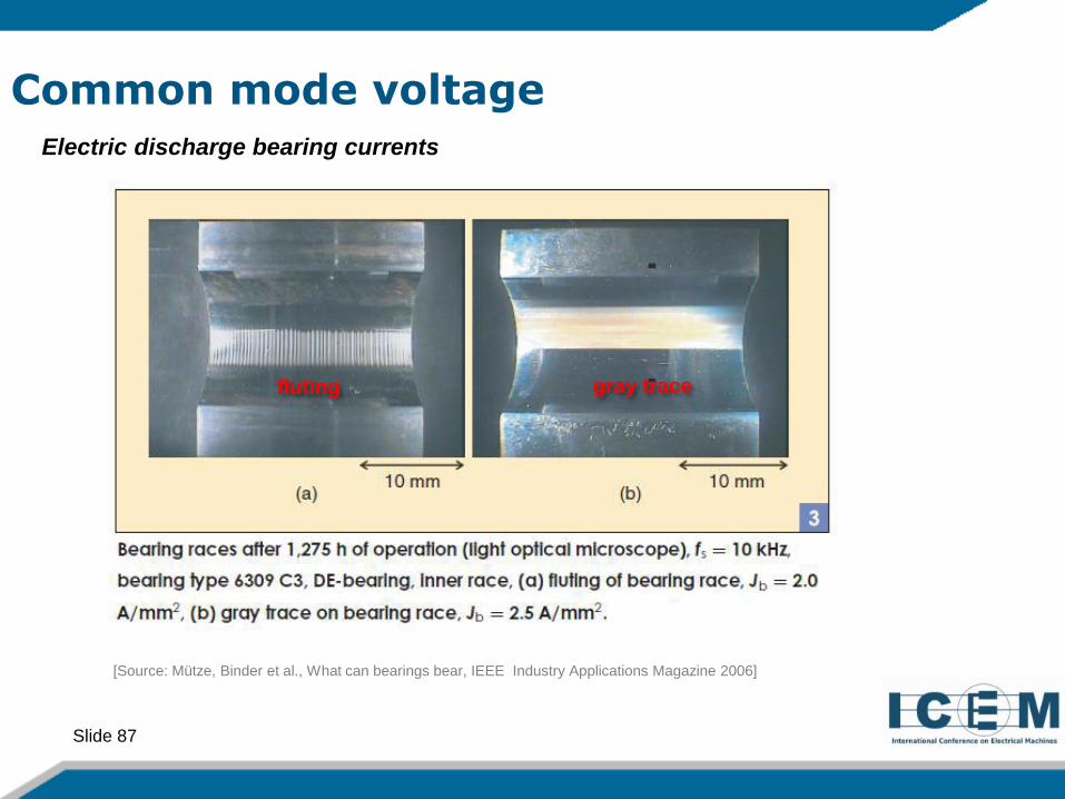
Electric discharge bearing currents
[Source of the waveforms: A. Binder, ICEM 2016 Tutorial]
Cb
Rb
Breakdown of lubricant
Slide 87
Common mode voltage
Electric discharge bearing currents
[Source: Mütze, Binder et al., What can bearings bear, IEEE Industry Applications Magazine 2006]
fluting gray trace

Slide 88
Common mode voltage
Electric discharge bearing currents
[Source: Tischmacher, Bearing Wear Condition Identification on Converter-Fed Motors, SPEEDAM 2018]
Different grades of bearing damages
Slide 89
Common mode voltage
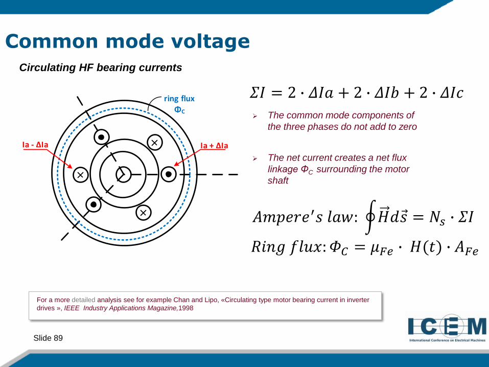
Circulating HF bearing currents
The common mode components of
the three phases do not add to zero
The net current creates a net flux
linkage ΦC surrounding the motor
shaft
𝑅𝑖𝑛𝑔 𝑓𝑙𝑢𝑥: 𝛷𝐶 = 𝜇𝐹𝑒 � 𝐻(𝑡) � 𝐴𝐹𝑒
𝐴𝑚𝑝𝑒𝑟𝑒′𝑠 𝑙𝑎𝑤: �𝐻𝑑𝑠 = 𝑁𝑠 � 𝛴𝐼
𝛴𝐼 = 2 � 𝛥𝐼𝑎 + 2 � 𝛥𝐼𝑏 + 2 � 𝛥𝐼𝑐
For a more detailed analysis see for example Chan and Lipo, «Circulating type motor bearing current in inverter
drives », IEEE Industry Applications Magazine,1998
Ia + ΔIaIa - ΔIa
ring flux ΦC
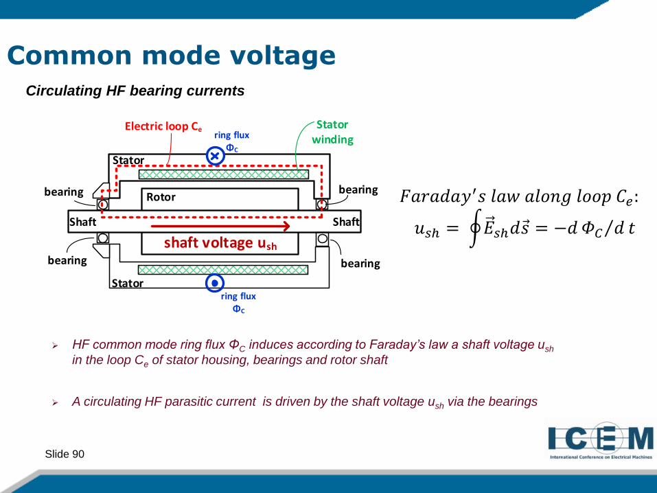
Slide 90
Common mode voltage
Circulating HF bearing currents
HF common mode ring flux ΦC induces according to Faraday’s law a shaft voltage ush
in the loop Ce of stator housing, bearings and rotor shaft
A circulating HF parasitic current is driven by the shaft voltage ush via the bearings
𝐹𝑎𝑟𝑎𝑑𝑎𝑦′𝑠 𝑙𝑎𝑤 𝑎𝑙𝑜𝑛𝑔 𝑙𝑜𝑜𝑝 𝐶𝑒:
𝑢𝑠ℎ = �𝐸𝑠ℎ𝑑𝑠 = −𝑑 ⁄𝛷𝐶 𝑑 𝑡
Stator winding
Stator
Stator
Rotor
ShaftShaft
bearing
bearing
Electric loop Ce
shaft voltage ush
ring flux ΦC
ring flux ΦC
bearing
bearing
Slide 91
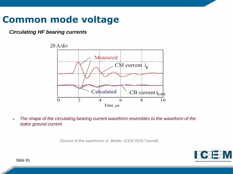
Common mode voltage
Circulating HF bearing currents
[Source of the waveforms: A. Binder, ICEM 2016 Tutorial]
The shape of the circulating bearing current waveform resembles to the waveform of the
stator ground current
Slide 92
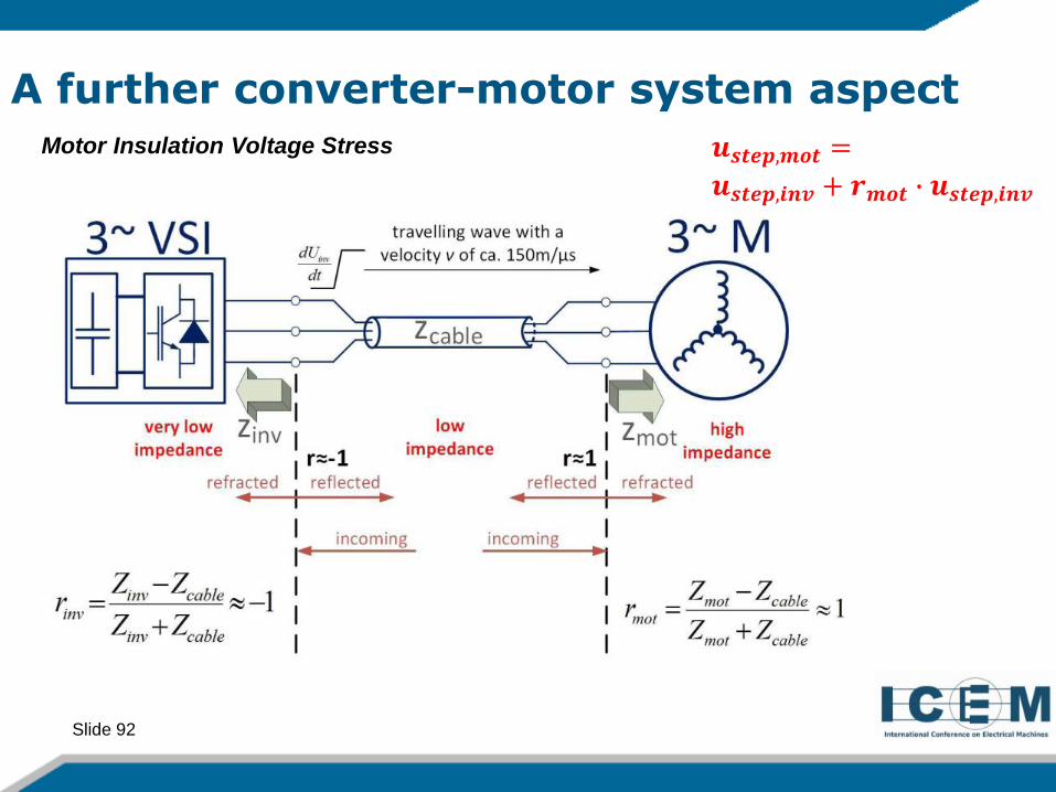
A further converter-motor system aspect
Motor Insulation Voltage Stress 𝒖𝒔𝒕𝒆𝒑,𝒎𝒐𝒕 =
𝒖𝒔𝒕𝒆𝒑,𝒊𝒏𝒗 + 𝒓𝒎𝒐𝒕 � 𝒖𝒔𝒕𝒆𝒑,𝒊𝒏𝒗

Slide 93
A further converter-motor system aspect Motor Insulation Voltage Stress
Oscillation of voltage at motor side due to wave reflection at
both ends of loss-free cable
The maximum possible voltage step at
the motor will appear if tr < 2 · tp,
where tr is the voltage rise time and
tp the propagation time
Critical length calculation:
𝒕𝒓 = 𝟐 � 𝒕𝒑= 𝟐𝒍𝒄𝒂𝒃𝒍𝒆
𝒗𝒑=> 𝒍𝒄𝒂𝒃𝒍𝒆 =
𝒗 � 𝒕𝒓
𝟐
𝒗𝒑 is approx. equal to half the
speed of light in vacuum, i.e.
150m/μs
For a rise time of 1μs the critical
length is approx. 75m
𝒗𝒐𝒍𝒕𝒂𝒈𝒆 𝒂𝒕𝒙 = 𝟎
𝒗𝒐𝒍𝒕𝒂𝒈𝒆 𝒂𝒕𝒙 = 𝒍𝒄𝒂𝒃𝒍𝒆
𝑽𝒅𝒄
𝑽𝒅𝒄
Slide 94
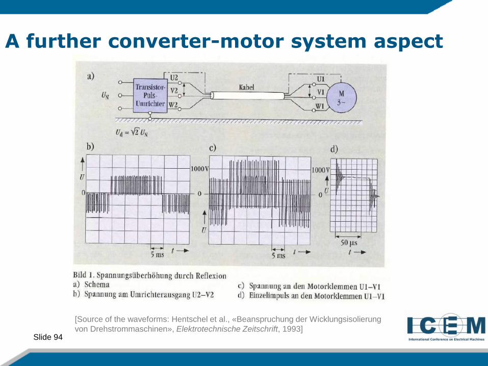
A further converter-motor system aspect
[Source of the waveforms: Hentschel et al., «Beanspruchung der Wicklungsisolierung
von Drehstrommaschinen», Elektrotechnische Zeitschrift, 1993]
Slide 95
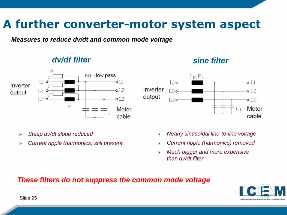
A further converter-motor system aspect
Measures to reduce dv/dt and common mode voltage
These filters do not suppress the common mode voltage
dv/dt filter
Steep dv/dt slope reduced
Current ripple (harmonics) still present
Nearly sinusoidal line-to-line voltage
Current ripple (harmonics) removed
Much bigger and more expensive
than dv/dt filter
sine filter

Slide 96
A further converter-motor system aspect
Measures to reduce dv/dt and common mode voltage
L-C low pass filter with direct connection to the DC link to suppress the common mode
harmonics
Usually available only for small power ratings
This type of filter reduces all paracitic HF current effects in the motor,
because the common mode voltage is reduced

Slide 97
Variable Speed Drives
Converter Topologies
Modulation Techniques
Evaluation Criteria and Important Drive System Aspects
Conclusion
Outline
Slide 98
Conclusion
The modulation is an important system parameter which influences significantly
the drive system performance
The selection of the appropriate modulation techniques for a specific drive
system and their distribution in a voltage-frequency table is a “system
optimization” issue
Drive system efficiency, motor noise and common mode voltage are important
system aspects that must be considered
The “converter-motor-load” entity must be considered as a whole in order to
optimize the distribution of the modulation techniques in the voltage-frequency
plane
Different voltage-frequency tables for different applications are necessary
System Optimization


![The aesthetic impact of graffiti art on modern Greek urban … · TSOUMAS, Johannis (2011): "The aesthetic impact of graffiti art on modern Greek urban landscape" [en línea]. En:](https://static.documents.pub/doc/80x56/5bf2b3b109d3f2de488b7371/the-aesthetic-impact-of-graffiti-art-on-modern-greek-urban-tsoumas-johannis.jpg)

