31
MODULE TITLE : DIGITAL & ANALOGUE DEVICES & CIRCUITS TOPIC TITLE : D.C. POWER SUPPLIES LESSON 2 : SMOOTHING
| Date post: | 25-Mar-2018 |
| Category: |
Documents |
| Upload: | phungthien |
| View: | 216 times |
| Download: | 2 times |

MODULE TITLE : DIGITAL & ANALOGUE DEVICES & CIRCUITS
TOPIC TITLE : D.C. POWER SUPPLIES
LESSON 2 : SMOOTHING
DADC - 3 - 2
© Teesside University 2011

Published by Teesside University Open Learning (Engineering)
School of Science & Engineering
Teesside University
Tees Valley, UK
TS1 3BA
+44 (0)1642 342740
All rights reserved. No part of this publication may be reproduced, stored in a
retrieval system, or transmitted, in any form or by any means, electronic, mechanical,
photocopying, recording or otherwise without the prior permission
of the Copyright owner.
This book is sold subject to the condition that it shall not, by way of trade or
otherwise, be lent, re-sold, hired out or otherwise circulated without the publisher's
prior consent in any form of binding or cover other than that in which it is
published and without a similar condition including this
condition being imposed on the subsequent purchaser.

________________________________________________________________________________________
INTRODUCTION________________________________________________________________________________________
Having described the construction and operation of transformers and rectifiers
in a d.c. power supply system, we now deal with the smoothing that is
necessary to produce a steady and sustainable d.c. supply.
________________________________________________________________________________________
YOUR AIMS________________________________________________________________________________________
On completion of this lesson you should be able to:
• explain the function of a 'reservoir' capacitor in a rectified d.c. supply
circuit
• define ripple factor and carry out simple related calculations
• state the advantages of incorporating an inductive component into a
'smoothing' circuit
________________________________________________________________________________________
STUDY ADVICE________________________________________________________________________________________
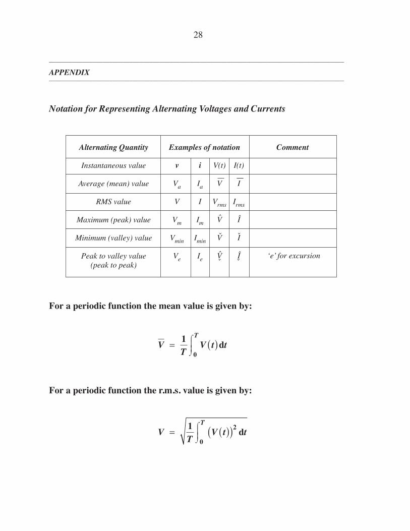
See the Appendix for the notation used for alternating quantities.
1
i i i i © T id U i it 2011

________________________________________________________________________________________
SMOOTHING________________________________________________________________________________________
The output from a rectifier circuit cannot be described as continuous direct
current because of the presence of a relatively large alternating component.
This form of output, particularly if resulting from full-wave rectification, is
suitable for some applications such as battery charging. However, in order to
be suitable for electronic equipment, the alternating component must be
reduced to a small percentage of the direct current output. This reduction
process is referred to as smoothing.
Smoothing is usually achieved by introducing a reactive component into the
circuit to 'filter' out most of the alternating component. The most common
method employs a shunt capacitor which is often referred to as a reservoir
capacitor because its function is similar to that of a pneumatic pressure vessel
or hydraulic accumulator.
CAPACITOR SMOOTHING
To achieve the smoothing process, the reservoir capacitor, C, is connected
across the rectifier output in parallel with the load, RL, as shown in FIGURE 1.
2
i i i i © T id U i it 2011

FIG. 1
The capacitor charges up near the peak of each rectified cycle and discharges
into the load for the remainder of the cycle. For a large part of each cycle,
therefore, the load current is being supplied by the reservoir capacitor whilst
the rectifier 'tops up' the capacitor charge at the peak of each cycle.
This effect is illustrated in the output waveform shown in FIGURE 2.
FIG. 2
Period T
Chargeperiod
Dischargeperiod
TC TD
0t
Loadvoltagev
RL
a.c.
Transformer
Reservoircapacitor
Full-wavebridge rectifier
LoadC
VsVD
VD
VL
3
i i i i © T id U i it 2011

RIPPLE
As FIGURE 2 shows, the supply of load current causes the capacitor voltage to
fall during each cycle. The resulting unevenness in d.c. output voltage is
termed ripple which appears as an alternating waveform superimposed on the
direct output.
A quantitative measure of the degree of ripple is the ripple factor (KV) which is
defined as:
or
where Vr is the r.m.s. value of the ripple voltage and the average load
voltage.
In order to simplify the calculations relating to ripple factor the following
approximations can be made.
• The output voltage waveforms can be assumed to be composed of
linear sections which produce a triangular or 'sawtooth' ripple
waveform as shown in FIGURE 3*.
________________________________________________________________________________________
*See the Appendix for the notation used for alternating quantities.
V L
KV
VVr
L= ......................................................... 1( )
KV = rms value of the a.c. voltage componentavverage value of the load voltage
4
i i i i © T id U i it 2011

FIG. 3
• Because the ripple voltage, Vr, will, in practice, be small compared
with the d.c. voltage, the discharge period, TD, can be assumed to
equal the total period, T. This allows approximation of the ripple
waveform to that shown in FIGURE 4.
FIG. 4
Evaluation of the a.c. voltage component can now be based on the rms value
(Vr) of one cycle of this 'ramp' waveform which can be calculated using
FIGURE 5.
time (s)Period T
Vrˆ̂
v
Period T
TD
t0
VL
VL
Vrˆ
ˆ̂
5
i i i i © T id U i it 2011

FIG. 5
The relationship between the instantaneous voltage, v, and the ripple voltage, Vr, can
be derived using similar triangles. See if you can write down this relationship.
....................................................................................................................................................
....................................................................................................................................................
....................................................................................................................................................
....................................................................................................................................................
....................................................................................................................................................
....................................................................................................................................................
________________________________________________________________________________________
v
t
V
T
v Vt
T
rr
r r
=
∴ =
∨
∧
∨
∧ ........................................ 3( )
VT
v tT
rms d ........................=⌠
⌡⎮⎮
1
0
2 ..... 2( )
T
v
t
Vr
0 t
v
6
i i i i © T id U i it 2011

Now substituting Equation (3) into Equation (2):
Substitution of Equation (4) into equation (1) gives the simple expression for
the voltage ripple factor:
Two other useful expressions are those for the ripple voltage, , and the
average d.c. output voltage, V L .
Vr∨
∧
K
V
VV
r
L= ∨
∧
3 .................................... 5( )
VT
Vt
Tt
V
Tt
r
T
r
r T
2
0
2
2
30
2
1=⎛⎝⎜
⎞⎠⎟
=
⌠
⌡⎮⎮
⌠
⌡⎮⎮
∨
∧
∨
∧
d
ddt
V
T
tV
T
T
V
r T r
r
=⎡
⎣⎢
⎤
⎦⎥ = ⎛
⎝⎜⎞⎠⎟
∴ =
∨
∧
∨
∧2
3
3
0
2
3
3
3 3
VV
V
V
r
r
r
2
3
3
∨
∧
∨
∧
= .......................................... 4( )
7
i i i i © T id U i it 2011

Ripple Voltage
During the charging period, the accumulated charge, ΔQ, in the capacitor is
given by the product of capacitance and voltage increase. Hence,
This same charge is transferred to the load, RL, during the discharge of the
capacitor. The transferred charge approximately equates to the product of the
average discharge current and discharge time. The average discharge current is
approximately the same as the average load current, (The validity of this
assumption is demonstrated later in the lesson.) Hence,
Combining Equations (6) and (7):
Substituting where f is the frequency of the original a.c. input,
gives:
VI
f CrL
∨
∧≈
2 .......................................... 8( )
Tf
= 12
CV I T
VI T
C
r L
rL
∨
∧
∨
∧
≈
∴ ≈
ΔQ I TL≈ ............................................ 7( )
I L .
ΔQ CVr=∨
∧ .......................................... 6( )
8
i i i i © T id U i it 2011

....................................................................................................................................................
....................................................................................................................................................
....................................................................................................................................................
....................................................................................................................................................
....................................................................................................................................................
________________________________________________________________________________________
The basic relationship between periodic time in seconds and frequency in hertz is
Because the frequency of the rectified waveform is twice that of the a.c. input waveform,
the relationship becomes
D.C. Output Voltage
Applying Ohm's law:
V f CR VL L r=∨
∧2 ............................ 10( )
Substituting for from Equation (8) givesI L ::
V I RL L L= .................................... 9( )
Tf
= 12
.
Tf
= 1.
Explain the relationship Tf
= 12
.
9
i i i i © T id U i it 2011

Example 1
A 24 V power supply delivers 200 mA to a resistive load. The a.c. supply is
240 V, 50 Hz and a bridge rectifier is used in conjunction with a 1000 μF
reservoir capacitor.
Estimate:
(a) the ripple voltage
(b) the transformer secondary voltage if the total diode forward voltage
drop in the rectifier is 1.3 V.
Solution
(a) Ripple voltage is given by:
(b) Reference to FIGURE 3 shows that the peak of the a.c. waveform is
given by:
where is the amplitude of the ripple voV r
∧lltage.
V V
V
V VL L
r
L r
∧ ∨
∧
∧= + = +
2
VI
f CrL
∨
∧=
= ×× × ×
=
2
200 102 50 1000 10
23
6
–
–.V
10
i i i i © T id U i it 2011

Allowing for the diode forward voltage drop, the peak transformer
secondary voltage, is given by:
Average d.c. Output Voltage of a FW Bridge Rectifier with Smoothing
The previous example (and with reference to FIGURES 1 and3) shows that:
where
Thus
V V V V V
V V V
V V V
L L r L r
L s D
L s D
= =
=
=
∧
∨
∧ ∧ ∧
∧
∧
– –
–
– –
12
2
2122
2
V
V V V V
r
L s D r
∨
∧
∧ ∧∴ = ................– – .............. 11( )
V V V
VV
S L D
SS
∧ ∧
∧
= +
= + = ( )
∴ = =
2
25 1 3 26 3
2
26 3
. .
.
V peak
22
18 6= . .V
V S
∧
∴ = +
∴ =
∧
∧
V
V
L
L
2422
25 V.
11
i i i i © T id U i it 2011

Peak Reverse Voltage of a Bridge Rectifier with Smoothing
The peak reverse-voltage (PRV) is the maximum reverse voltage that the
bridge circuit can produce across the rectifying diodes. The voltage rating of
the diode must be in excess of the PRV to prevent voltage breakdown
In the case of the bridge rectifier, the PRV can be found by consideration of the
circuit of FIGURE 6 which shows one pair of diodes conducting and the other
pair reverse-biased.
FIG. 6
The PRV is given by the voltage across the points ×-× of the circuit. Denoting
the PRV by the symbol (for repetitive reverse voltage), then is
given by:
V V VRR L D
∧ ∧= +
V RR
∧V RR
∧
Vs
X
X
VL
VD
Vxx
12
i i i i © T id U i it 2011

For FW rectification:
Note again that is a property of the circuit, not the rating of the diode. To
avoid damage, the diode’s reverse-voltage rating should be somewhat in excess
of .
CAPACITOR RIPPLE CURRENT IN A FW BRIDGE RECTIFIER
The charging current in the smoothing capacitor of FW rectifier consists of a
series of pulses as shown in FIGURE 7. Current only flows into the capacitor
during the brief period for which the rectifier output voltage exceeds the load
voltage, i.e. during the charging period TC. This effect is problematic in
several respects:
• the smoothing capacitor will have to have a high ripple current rating
• the current in the rectifying diodes will also consists of pulses of
current and the diodes will therefore have to have a suitable surge
current rating
V RR
∧
V RR
∧
V VRR s
∧ ∧� ................................................ 13( )
Assuming then:V Vs D
∧>> ,
V V V
V V V
L s D
RR s D
∧ ∧
∧ ∧
=
∴ =
–
–
2
...................................... 12( )
13
i i i i © T id U i it 2011

• the high peak values of current will cause a large volt drop across the
transformer windings
• the I2R power loss in the transformer will be greater than it would be
for an average current passed over the entire cycle, requiring a
transformer with a higher VA rating.
FIG. 7
During the discharge period the capacitor provides the entire load current.
This is because during discharge the diode anode voltage falls below the
voltage across the capacitor and the diode is reverse-biased. Thus, the
capacitor’s current decays exponentially to the equation
iLRLC
i i
I It
CRI
DC L
L LL
L
=
= ⎛⎝⎜
⎞⎠⎟
⎛⎝⎜
⎞⎠⎟
+∧ ∨ ∨
– exp –
Period T
Chargeperiod
Dischargeperiod
TC TD
0t
Loadvoltage
v/vo
lts
Pulse ofcharging current
I/am
ps
14
i i i i © T id U i it 2011

This exponential decay of
current is represented in the
lower curve of the sketch of
FIGURE 8.
In practice, because of the
long time constant CRL, this
curve can be, to a very good
approximation, regarded as
being a straight line. Indeed, more often than not, the discharge current can
assumed to be constant, as represented by the upper horizontal dotted line.
This assumption can be seen to be justified the PSpice simulation of a bridge
rectifier with smoothing shown in the circuit of FIGURE 9(a)1. Here the
primary of a 20:1 turns ratio transformer is connected to a 240 V, 50 Hz supply.
Thus the secondary voltage is 10 V (rms). Current and voltage waveforms for
the circuit are plotted in FIGURE 9(b). Note that the diode pairs conduct every
other cycle and the diode current consists of a pulse whilst the capacitor is
charging. For a load of 100 Ω, this pulse has a peak value of over 1.4 amps,
whereas the load current is little more than 100 mA; the bulk of the diode current
is flowing into the capacitor. That this is so can be seen in the waveform for the
capacitor current. This consists of a pulse of current during the charging period
that is IL less than the diode current, i.e. the diode supplies both the charging
capacitor and the load currents. During discharge the capacitor supplies the load
current (this is represented as a negative current in the waveform, as positive
current has been assumed to be flowing into the capacitor).
________________________________________________________________________________________
1Note the following points in relation to the use of PSPICE:
The transformer model used is ideal and PSPICE requires resistance (R2) to be included in the primary
winding to prevent this winding appearing as a short circuit to the voltage source. Similarly for the analysis to
run, the secondary circuit will have to be ‘earthed’, although of course this might not be the case in practice.
The load voltage has been measured using a ‘differential voltage probe’ as a single-ended voltage probe will
measure the voltage with respect to the earth point.
TDC
FIG. 8
IL
IL
ˆˆ
15
i i i i © T id U i it 2011

For C = 1 mC and RL = 100 Ω, the ripple voltage can be seen to be about
±500 mV.
From the information given in FIGURE 9, estimate the forward volt drop across the
diodes.
FIG. 9(a)
16
i i i i © T id U i it 2011

FIG. 9(b)
Dio
de c
urre
nt/a
mps
1.4
1.2
1
0.8
0.6
0.4
0.2
0
Time/Secs 2mSecs/dw1 1.002 1.004 1.006 1.008 1.01 1.012 1.014 1.016 1.018
Time/Secs 2mSecs/dw1 1.002 1.004 1.006 1.008 1.01 1.012 1.014 1.016 1.018
Cap
aici
tor
curr
ent/
amps
1.2
1
0.8
0.6
0.4
0.2
0
–0.1
Seco
ndar
y vo
ltag
e/vo
lts
10
5
0
–5
–10
Time/Secs 2mSecs/dw1 1.002 1.004 1.006 1.008 1.01 1.012 1.014 1.016 1.018
Time/Secs 2mSecs/dw1 1.002 1.004 1.006 1.008 1.01 1.012 1.014 1.016 1.018
Rip
ple
volt
age/
volt
s
13
12.8
12.6
12.4
12.2
17
i i i i © T id U i it 2011

From equation (11):
Thus
Therefore
CHOKE INPUT FILTER
The use of a reservoir capacitor produces minimum ripple and maximum d.c.
output when the output resistance is relatively high. A reduction in load
resistance, therefore, will cause an increase in the ripple factor.
This effect can be reduced by introducing an inductor into the smoothing
circuit. An inductive element in the circuit will reduce the ripple voltage when
the load resistance falls and the ratio of ωL to R increases.
The circuit is shown in FIGURE 10.
FIG. 10
The inclusion of a series inductance will also reduce any 'surge' effects which
may occur and possibly remove the need for any additional surge current
protection.
RL
L
CInputfrom
rectifier
VV V V
V
V
rD
s DC
D
D vo
=
=
=
∧ ∧– –
. – . – .
.
2
14 14 0 5 12 62
0 52 llts
18
i i i i © T id U i it 2011

________________________________________________________________________________________
NOTES________________________________________________________________________________________
...................................................................................................................................................
...................................................................................................................................................
...................................................................................................................................................
...................................................................................................................................................
...................................................................................................................................................
...................................................................................................................................................
...................................................................................................................................................
...................................................................................................................................................
...................................................................................................................................................
...................................................................................................................................................
...................................................................................................................................................
...................................................................................................................................................
...................................................................................................................................................
...................................................................................................................................................
...................................................................................................................................................
...................................................................................................................................................
...................................................................................................................................................
...................................................................................................................................................
...................................................................................................................................................
...................................................................................................................................................
...................................................................................................................................................
...................................................................................................................................................
...................................................................................................................................................
...................................................................................................................................................
...................................................................................................................................................
...................................................................................................................................................
...................................................................................................................................................
...................................................................................................................................................
...................................................................................................................................................
...................................................................................................................................................
19
i i i i © T id U i it 2011

________________________________________________________________________________________
SELF-ASSESSMENT QUESTIONS________________________________________________________________________________________
1. Explain what is meant by the following terms:
(a) peak-to-peak ripple voltage
(b) rms ripple voltage
(c) ripple factor.
2. A full-wave rectifier has an input voltage of 30 volts (rms) at 50 Hz. If a
500 μF smoothing capacitor is used across a load resistance of 100 Ω,
calculate the following:
(a) the rms ripple voltage
(b) the average voltage across the load
(c) the d.c. load current
(d) the ripple factor
(e) the maximum reverse-bias voltage applied to the diode.
3. A full-wave bridge rectifier with a 1000 μF shunt capacitor. It is required
to supply a load resistance with an average d.c. voltage of 20 volts with a
maximum peak-to-peak ripple voltage of 2 volts. If the supply frequency
is 50 Hz, calculate:
(a) the rms input voltage to the rectifier
(b) the minimum load resistance
(c) the PRV across each diode.
20
i i i i © T id U i it 2011

________________________________________________________________________________________
NOTES________________________________________________________________________________________
...................................................................................................................................................
...................................................................................................................................................
...................................................................................................................................................
...................................................................................................................................................
...................................................................................................................................................
...................................................................................................................................................
...................................................................................................................................................
...................................................................................................................................................
...................................................................................................................................................
...................................................................................................................................................
...................................................................................................................................................
...................................................................................................................................................
...................................................................................................................................................
...................................................................................................................................................
...................................................................................................................................................
...................................................................................................................................................
...................................................................................................................................................
...................................................................................................................................................
...................................................................................................................................................
...................................................................................................................................................
...................................................................................................................................................
...................................................................................................................................................
...................................................................................................................................................
...................................................................................................................................................
...................................................................................................................................................
...................................................................................................................................................
...................................................................................................................................................
...................................................................................................................................................
...................................................................................................................................................
...................................................................................................................................................
21
i i i i © T id U i it 2011

________________________________________________________________________________________
ANSWERS TO SELF-ASSESSMENT QUESTIONS________________________________________________________________________________________
1. (a) The peak to peak ripple voltage is the maximum variation in output
voltage and is denoted by
(b) The rms ripple voltage is the value (as would be indicated by an a.c.
voltmeter if connected across the load) which is given by:
(c) The ripple factor is the ratio between the rms ripple voltage and the
average d.c. voltage:
ripple factor = ( )V
Vr rms
DC
VV
V
r rmsr
r
( )
∧∨
∧
= =3 2 3
Vr∨
∧.
22
i i i i © T id U i it 2011

2. (a)
(b)
VL = 36.92 volts
V V VL C r=
=
∧
∨
∧–
. –.
12
41 038 21
2
Vr∨
∧= 2.37 volts
V V VC s D
∧ ∧=
=
2
42
–
.. – .
.
43 2 0 7
41 03
12
( )
=
=⎛⎝⎜
⎞⎠⎟∨
∧ ∧
volts
Vf CR
VrS L
C
==× × × ×
⎛⎝⎜
⎞⎠⎟
=
12 50 500 10 100
41 03
8 21
6–.
. volts
Vr rrms
rV
( )∨
∧
=
=
2 3
8 21
2 3
.
23
i i i i © T id U i it 2011

(c)
(d)
(e)
VRR = 41.73volts
PRV, V V VRR s D=
=
∧–
. – .42 43 0 7
Ripple factor 0.064=
Ripple factor =
=
( )V
V
r rms
L
2 3736 92
..
I L = 369 mA
IV
RLL
L
=
= 36 92100
.
24
i i i i © T id U i it 2011

3. (a)
The rms value of a sinusoidal voltage is equal to its peak value
divided by the square root of two, therefore:
Vs rms( ) = 15.84 volts
VV
s rmss
( )
∧
=
=
2
22 4
2
.
V V V
V V V
L C r
C L r
=
∴ = +⎛⎝⎜
⎞⎠⎟
= +
∧
∨
∧
∧
∨
∧
–12
12
2012
××⎛⎝⎜
⎞⎠⎟
=
=
∴
∧
2
21
2
volts
since:
V V VC s D–
VV V Vs C D= +
= + ×( )
=
∧2
21 2 0 7
22 4
.
. volts
25
i i i i © T id U i it 2011

(b)
This will equal the minimum value of load resistance because a
smaller RL value will result in a higher ripple voltage
(c)
VRR = 21.7 volts
PRV, V V VRR s D=
=
∧–
. – .22 4 0 7
RL min( ) = 105 Ω
Vf CR
V
Rf CV
rL
C
Lr pk pk
∨
∧ ∧
( )
=⎛⎝⎜
⎞⎠⎟
⇒ =⎛
⎝⎜
⎞
⎠⎟
12
12 –
VV C
∧
=× × ×( ) ×
⎛
⎝⎜⎞
⎠⎟
=
12 50 1000 10 2
21
105
6–
Ω
26
i i i i © T id U i it 2011

________________________________________________________________________________________
SUMMARY________________________________________________________________________________________
• A filter reduces the output d.c. voltage variation from a rectifier. This
voltage variation is referred to as ripple voltage.
• The simplest type of filter consists of a capacitor connected in parallel
(shunt) across the output terminals of the rectifier – this capacitor can be
referred to as a reservoir capacitor.
• Higher smoothing capacitance results in:
smaller ripple voltage
higher average load d.c. voltage.
• Ripple voltage is also dependant on load resistance, i.e. as a load
resistance decreases, then ripple voltage will increase.
• Average load voltage, V V VL C r=∧
∨
∧–
12
•• Peak reverse voltage (PRV) V VRR =∧
ss DV– 2
• Peak-to-peak ripple voltage Vfr∨
∧=
12 CCR
VL
C
∧
• Ripple factor =V
Vr rms
DC
( )
where Vr rms
rV
( )∨
∧
=2 3
27
i i i i © T id U i it 2011
________________________________________________________________________________________
APPENDIX________________________________________________________________________________________
Notation for Representing Alternating Voltages and Currents
For a periodic function the mean value is given by:
For a periodic function the r.m.s. value is given by:
VT
V t tT
= ( )( )⌠
⌡⎮⎮
1
0
2d
VT
V t tT
= ( )⌠
⌡⎮⎮
1
0d
Alternating Quantity
Instantaneous value
Average (mean) value
RMS value
Maximum (peak) value
Minimum (valley) value
Peak to valley value(peak to peak)
Examples of notation Comment
v
Va
V
Vm
Vmin
Ve
i
Ia
I
Im
Imin
Ie
V(t)
V
Vrms
V
V
V
I(t)
I
Irms
Î
I
Î ‘e’ for excursionˆ
ˆ
ˆ ˆ
ˆ ˆ
28
i i i i © T id U i it 2011

Labelling applied to a sinusoid:
Labelling applied to a ripple present in a d.c. voltage:
V
t0
v
V
ˆ
Vmin V̂Vm
ˆ̂
t0
v
v = Vm sin(ωt)
Ve V̂ˆ
V̂Vm
29
i i i i © T id U i it 2011


