STRUCTURAL INTEGRITY OF A 3D TSV PACKAGE UNDER THERMAL LOADING: A STRUCTURAL MECHANICS BASED STUDY Mohammed Shahid Ali, A.R Nazmus Sakib, Dereje Agonafer. The University of Texas at Arlington.
Transcript
STRUCTURAL INTEGRITY OF A 3D TSV PACKAGE UNDER THERMAL LOADING: A STRUCTURAL MECHANICS BASED STUDY
Mohammed Shahid Ali, A.R Nazmus Sakib, Dereje Agonafer.The University of Texas at Arlington.
Trend in 3D packaging 3D TSV Package Introduction and challenges. Issues addressed in this paper.
• Modeling descriptions, methodology and properties.• Crack formulation methodology in ANSYS and cut
boundary application to model.• Variation of die and substrate thickness and its
effects. Validation and Results. Conclusion.
Overview
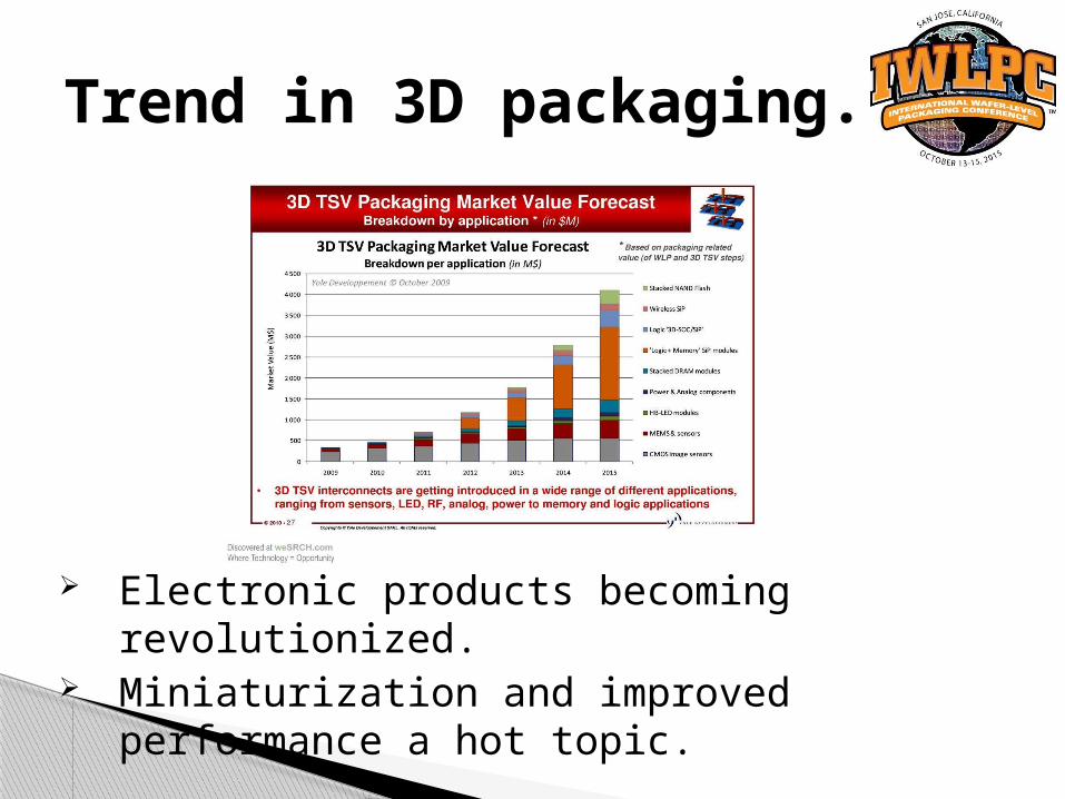
Electronic products becoming revolutionized. Miniaturization and improved performance a hot
topic.
Trend in 3D packaging.
3D TSV technology advantages: Increased performance. Reduced form factor. Cost reduction. High-bandwidth interconnection between stacked
chips.
Trend in 3D packaging.
3D TSV technology still faces some issues.
CTE mismatch issues and its effects.
Critical areas in TSV package.
Limitations & Challenges
Motivation for this work.
Crack propagation in 3D TSV package & calculation of SIF in silicon die.
Methodology used (FEM, submodeling technique).
Variation of die and substrate thickness.
Some Issues Addressed in This Paper-
A 2 die 3D flip chip package with TSV.
Modeled using linear elastic properties.
Modeling Technique (diameter and dielectric, CRE).
Simulation steps.
Symmetry boundary conditions and constraints.
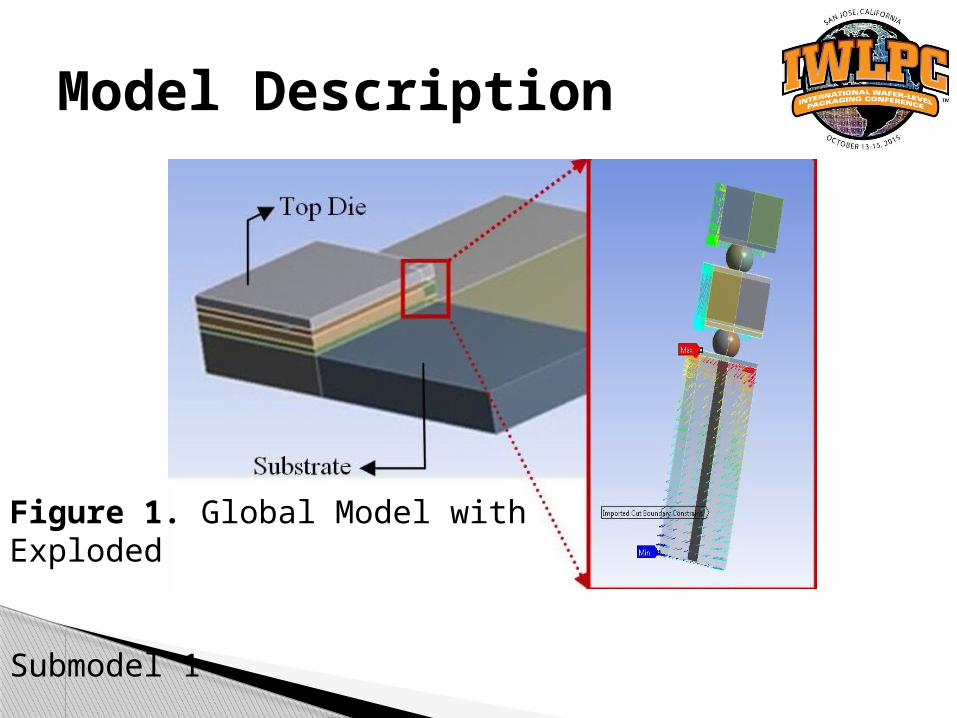
Model Description
Model Description
Figure 1. Global Model with Exploded Submodel 1
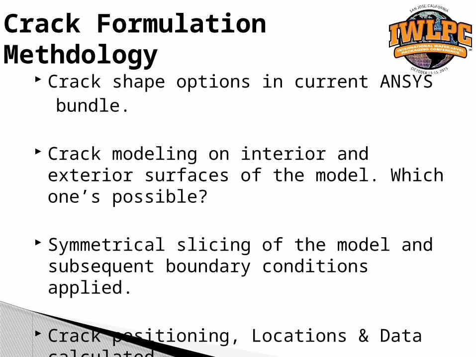
Crack shape options in current ANSYS bundle.
Crack modeling on interior and exterior surfaces of the model. Which one’s possible?
Symmetrical slicing of the model and subsequent boundary conditions applied.
Crack positioning, Locations & Data calculated.
Crack Formulation Methdology
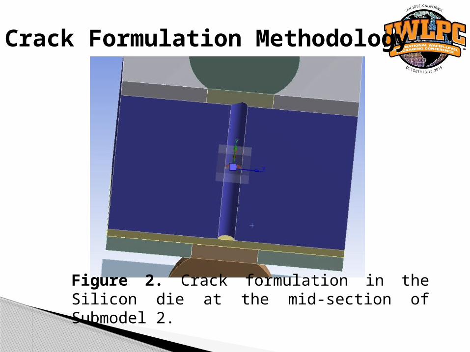
Crack Formulation Methodology
Figure 2. Crack formulation in the Silicon die at the mid-section of Submodel 2.
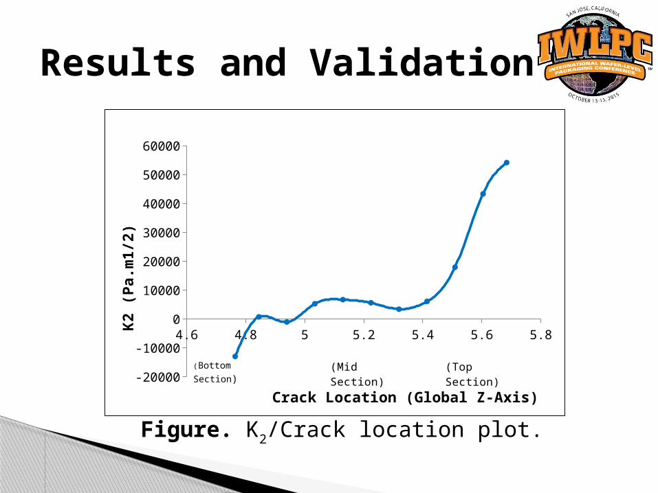
Results and Validation
Figure. SIF (K2) distribution at crack location in Submodel 2.
Results and Validation
4.6 4.8 5 5.2 5.4 5.6 5.8
-50000
-40000
-30000
-20000
-10000
0
10000
20000
Crack Location (Global Z-Axis)
K1
(P
a.m
1/2
)
(Top Sec-tion)
(Mid Section)(Bottom Section)
Figure. K1/Crack Location plot.
Results and Validation
4.6 4.8 5 5.2 5.4 5.6 5.8
-20000
-10000
0
10000
20000
30000
40000
50000
60000
Crack Location (Global Z-Axis)
K2
(P
a.m
1/2
)
(Top Section)(Mid Section)(Bottom Section)
Figure. K2/Crack location plot.
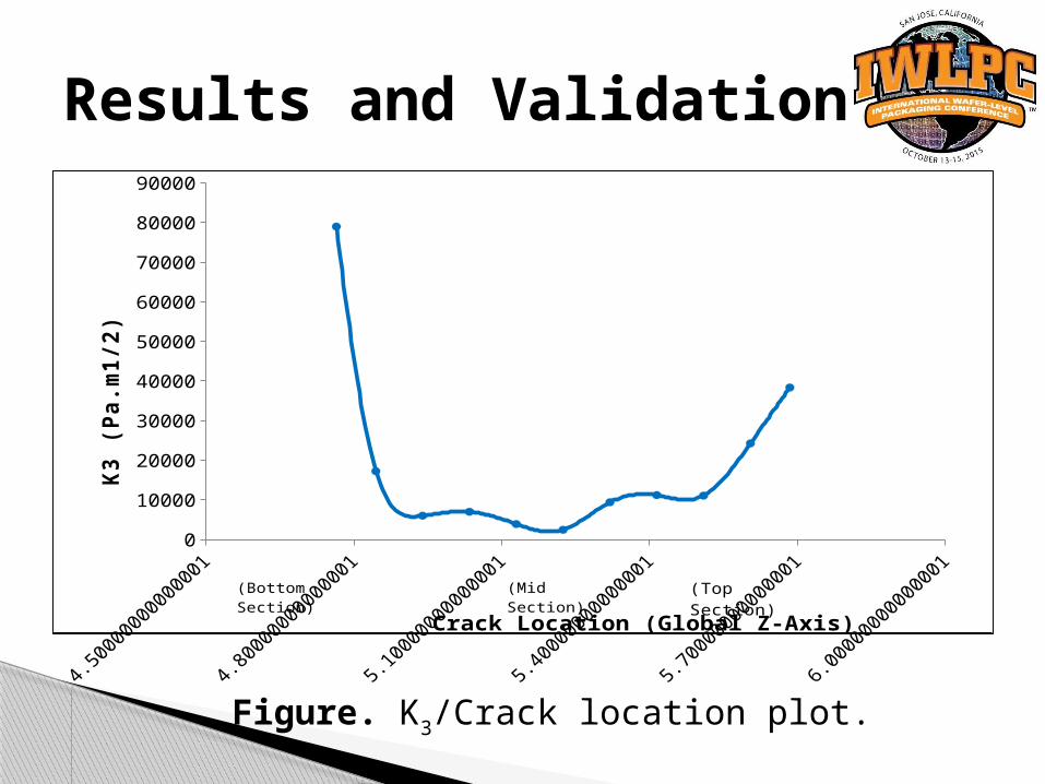
Results and Validation
0
10000
20000
30000
40000
50000
60000
70000
80000
90000
Crack Location (Global Z-Axis)
K3
(P
a.m
1/2
)
(Top Section)(Mid Section)(Bottom Section)
Figure. K3/Crack location plot.
Analysis on crack driving force.
Variation of Die and Substrate Thickness
0.2 0.3 0.4 0.5 0.6 0.7 0.8 0.9 1 1.1-5.00E-03
-5.20E-18
5.00E-03
1.00E-02
1.50E-02
2.00E-02
2.50E-02
3.00E-02
Substrate Thickness (mm)
J-I
nte
gra
l (J
/m2
)
Figure. J-Integral vs Substrate Thickness Plot
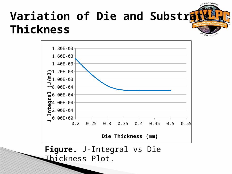
Variation of Die and Substrate Thickness
0.2 0.25 0.3 0.35 0.4 0.45 0.5 0.550.00E+00
2.00E-04
4.00E-04
6.00E-04
8.00E-04
1.00E-03
1.20E-03
1.40E-03
1.60E-03
1.80E-03
Die Thickness (mm)
J I
nte
gra
l (J
/m2
)
Figure. J-Integral vs Die Thickness Plot.
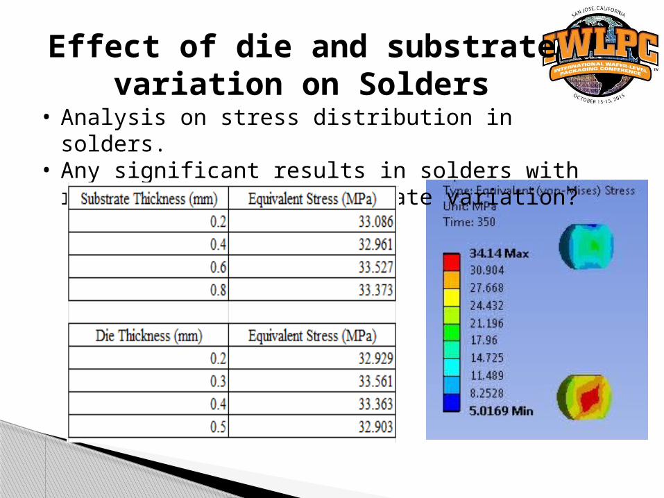
Effect of die and substrate variation on Solders
• Analysis on stress distribution in solders.• Any significant results in solders with respect to die
and substrate variation?
Conclusions Successfully modeled crack in the interior of
TSV/Silicon interface with subsequent submodels and cut boundary constraints.
Critical areas where K1, K2, K3 are prominent are highlighted.
SIF values compared with fracture toughness of silicon.