Proc. 4th Int’l. Cod. on Calorimetry in High Energy Physics, 143-147 (1994) World Scientific, A. Menzione & EA. Scribano, e&. MONOLITHIC FRONT-END PREAMPLIFIERS FOR A BROAD RANGE OF CALORIME’IRY APPLICATIONS* V. Radeka and S. Rescia Brookhaven National Laboratory Upton, NY 11973-5000 P. F. Manfredi and V. Speziali Dipartimento di Elettronica Via Abbiategrasso 209 - 27100 Pavia, Italy and INFN - Sezione di Milano, Via Celoria 16 - 20133 Milano, Italy 1993 1 This work was supported by the U. S. Department of Energy: Contract No. DE-AC02-76CH00016 and by the Italian MURST 40% program. ,. I
Transcript
Proc. 4th Int’l. Cod. on Calorimetry in High Energy Physics, 143-147 (1994) World Scientific, A. Menzione & EA. Scribano, e&.
MONOLITHIC FRONT-END PREAMPLIFIERS FOR A BROAD RANGE OF CALORIME’IRY APPLICATIONS*
V. Radeka and S. Rescia Brookhaven National Laboratory
Upton, NY 11973-5000
P. F. Manfredi and V. Speziali Dipartimento di Elettronica
Via Abbiategrasso 209 - 27100 Pavia, Italy
and
INFN - Sezione di Milano, Via Celoria 16 - 20133 Milano, Italy
1993
1
This work was supported by the U. S. Department of Energy: Contract No. DE-AC02-76CH00016 and by the Italian MURST 40% program.
, . I
... .. .
MONOIJTRIC FRONT-END PREAMPLIFIERS FOR A BROAD RANGE OF CALORMEIRY APPLICATIONS*
V. W E K A , S . RESCIA Brookhaven Nationul Laboratory
Upton. N.Y. I1973
P.F. MANFREDI, V. SPEZlALI Dipartimento a'i Elenronica, Via Abbiategrasso 209 - 27100 Pavia, Italy
and INFN - Sezwne di Milano, Via Celoria 26 - 20133 Milano. Italy
ABSTRACT
The present paper summarizes the salient results of a research and development activity in the area of low noise preamplifiers for different applications in calorimetry. Design target for all circuits considered here are low noise, abiity to cope with broad energy ranges and radiation hardness.
1. Introduction
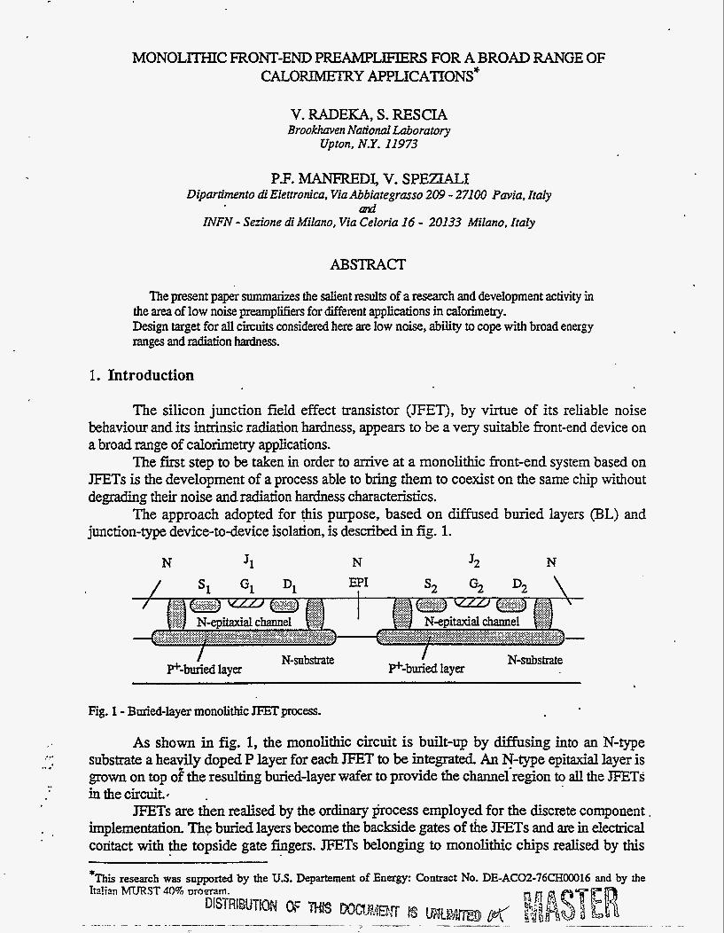
The silicon junction field effect transistor (JFET), by virtue of its reliable noise behaviour and its inwinsic radiation hardness, appears to be a very suitable front-end device on a broad range of calorimetry applications.
The first step to be taken in order to arrive at a monolithic front-end system based on JFETs is the development of a process able to bring them to coexist on the same chip without degrading their noise and radiation hardness characteristics.
The approach adopted for this purpose, based on diffused buried layers (BL) and junction-type device-todevice isolation, is described in fig. 1.
N
/ Sl
'1
Gl Dl
N EPI
I
'2
s 2 G2
N
D2 \
1 €?+-buried layer N-substrate
Fig. 1 - Buried-layer monolithic JFET process.
As shown in fig. 1, the monolithic circuit is built-up by diffusing into an N-type substrate a heavily doped P layer for each JFET to be integrated. An N-type epitaxial layer is grown on top of the resulting buried-layer wafer to provide the channel-region to all the m T S in the circuit..
implementation. The buried layers become the backside gates of the JFETs and are in electrical contact with the topside gate fingers. JFETs belonging to monolithic chips realised by this
JFETs are then realised by the ordinary process employed for the discrete component ,
process were proven to closely track their discrete equivalents from the standpoints of noise and its sensitivity to radiation [l, 2J.
In fig. 2 the noise voltage spectral densities of a discrete JFET (hterfet NJ132L) (a) and the corresponding part of the buried-layer process @), are compared+ in conditions of equal transconductance (8.5 mA/v). The comparison shows that the two spectra overlap in the high frequency =@on, where the spectral density is governed by the channel t h e d noise and in the very low Ikquency region. The larger noise voltage density exhibited by the monolithic part in the IO-to-100 Hz range seems to be attributed to a slightly higher Iff contribution [3].
I D = l m A
a? . .
YL
0.1 - 10 lo2 103 10" 16 io6 io7
Fig. 2 - Noise voltage spectraI densities of a discrete NJ132L (a) and the corresponding part of the buried-layer iJ== (w = 28oo w) (b).
Only N-channel can be integrated in the present version of the BL process, so the circuit design cannot rely upon complementary devices.
Merent types of monolithicpreamplifiers have been developed and thoroughly tested. According to the results of the measmmenk, the spectral density on the high frequency noise referred to the input of the whole ampEer exceeds the theoretically expected channel thermal noise in the input JFET by a few percent. The monolithic preamplifiers tested so far were found to be functional, with negligible variations in their static and small-Signal characteristics after more than 30 Mrad integrated dose of ~ C O y-rays and 1014 neutron fluence. Radiation tests so far have been carried out at room temperature. At shaping times in the.20-to-50 ns range the resulting ENC degradation is negligibly small in the y-ray case and stiU acceptable in the case of neutrons.
New design concepts have emerged from the analysis of the situations that may occur in cdorimeq applications with cryogenic liquids at very high energies. A real difficulty comes from the very large dynamic range the preamplifier has to cope with. To overcome this, at least up to a certain limit, the use of a smaU feedback resistor was proposed as a possible solution. Beyond this Limit, the use of a nonlinear feedback network becomes essential. Its introduction, however, requires a reconsideration of the basic preamplifier structure.
2. Basic Preamplifiers for CaIorirnetry
The monolithic preamplXers are intended for calorimetry applications with weighting functions spanning from tens of nanoseconds to several microseconds. A large low-frequency gain, around 80 dB, was accordingly assumed as a design target in order to ensure a high
\
accuracy at long processing times. This is the reason for the active load configuration of the
In the circuit of fig. 3 J1 and 52 are a cascode whose output signal current is injected across the high impedance load consisting of the current source J3 bootstrapped by J7 and 54. To make such a bootstrapping action more effective, a high impedance load is provided on the source of J7 (35,56). J7 buffers the signals on the J2 drain and transmits it to the output source follower Jg.
drain of JEET J2 in fig. 3.
i - -6V Fig. 3 - Monolithic preamplifier circuit diagram. The W values are shown for each JFET in the circuit.
Although resistors and capacitors can be integrated in the BL process, it was preferred in the present preamplifier version to add the bias resistors R1, R2, the feedback elements RF, CF and the RBL resistor as off-the-chip components.
In the closed-loop configuration the reference current set by J3 flows through Je, J4 and J1. The current in J1 can be adjusted above this value by acting on RBL. This allows a control of the transconductance of J1 and therefore of its channel thermal noise.
The transistors on the signal path, (51, Jz, J7, Jg), to meet the requirement of a large gain-bandwidth product are realised as shorter channel devices, with a source-to-drain spacing of 15 pm (5 pm-gate length). Transistors J3, 54, J5, J6, that implement active loads and for which a small output conductance is an important characteristic, are units of longer source-to- chin spacing, about 25 pm (7 pm-gate length).
The preamplifier of fig. 3 is available in two versions. One, lab&ed H, where H indicates high resistivity, employs a channel region of 1.3 to 1.9 ohm -cm and is intended for operation at liquid Ar temperature. The other one, labelled L, has a channel resistivity of about 0.5 ohm-cm and is suitable for operation Eromroom temperature down to LKr.
At room tempemure the L-type preamplifier has a larger transconductance in the input device, which results in a higher dc forward gain, beyond 80 d& against 75 dB in the H-type preamplifier, and a smaller high-frequency noise.
The typical room temperature spectral noise density referred to the input for the two circuit types is described in fig. 4.
f m1
- 10 G! s -7
E 2, .d rA
P 8 1
IO 102 ' id io4 1 ' fW1
~
Fig. 4 - Spectral density of the input-referred noise: a) E-type preamplifier, b) L-type preamplifier.
So far, only L-type preamplifier has been throughly characterised from the standpoints of the noise behaviour at different temperatures and noise sensitivity to the absorbed radiation.
The results of equivalent noise charge (ENC) measurements carried out at different temperatures are plotted in fig. 5. They refer to the situation where a capacitor of 480 pF is connected at the preamplifier input to simulate the detector and a shaper employing two RC integrators and two CR differentiators to provide a bipolar weighting function with 50 ns peaking time is employed at the preamplifier output.
16000
14000
u 10000
8000
6000
Fig. 5 - ENC as a function of the temperature.
Radiation tests have been carried out so far on the L-type preamplifier exposed at room temperature to ~ C O 'y-rays and to neutrons. The ENC degradation at different values of the peaking t h e tp is shown in fig. 6 a) and b). The ENC measurements were carried out, as 31 the case of fig. 5, with a 480 pF capacitor at the PreampLifier input and an (RC)2-(CR)2 filter following the preampmer.
The behaviour of ENC as a function of tp in the irradiated preamplifier is in either case consistent with the hypothesis that the degradation be due to an increase in the low frequency noise related to the change of state of traps created by the radiation. It is interesting, in this respect, to observe the behaviour of ENC in a preamplifier which, after being irradiated at room
t
teriperatpre, is cooled.
L
tp Ins3
ld I ' ' ' .....i, . . . . .... i * , * .....
Fig. 6 - ENC as a function of the peaking time $, before and after inradiation: a) 6oCo ?-rays, b) 6 MeV neutrons.
Such a behaviour is described in fig. 7 and refers to the case of neutron irradiation with a fluence of 4 loi4 cm-2.
Fig.7- EI 2 values for a preamplifier irradiated at mom temperature up to a fluence of 4 IO1' cm2 6 MeV neutrons and then cooled.
The point at the extreme right is the value of ENC before irradiation. D e other points correspond to the ENC values measured at decreasing temperatures. As shown in fig. 7, once T is reduced below 128 K, ENC has recovered the value it had before irradiation. This can be put in connection with the fact that the probability of changes in the charge state of the traps created by irradiation drops when the device is cooled below a cer& temperature.
3. Acknowledgements
The authors are indebt to V. Re for his contribution throughout this work and to L. Fabris who carried out the characterisation of devices and Circuits.
4. References
1. V. Radeka, S. Rescia, P.F. Manfkdi, V. Speziali, F. SveIto, 7EEE Trans. Nucl. Sci. NS 40 (4) (1993) 744. 2. V. Radeka, S. Rescia, P.F. Manfredi, V. Re, V. Speziali, Nucl. Instr. and Meth. A326 (1993) 77. 3. K. Kandiah and F.B. Whiting, Nucl. Znstr. and Meth. A326 (1993) 49.
DISCLAIMER
This report was prepared as an account of work sponsored by an agency of the United States Government. Neither the United States Government nor any agency thereof, nor any of their employees, makes any warranty, express or implied, or assumes any legal liability or responsi- bility for the accuracy, completeness, or usefulness of any information, apparatus, product, or process disclosed, or represents that its use would not infringe privately owned rights. Refer- ence herein to any specific commercial product, process, or service by trade name, trademark, manufacturer, or otherwise does not necessarily constitute or imply its endorsement, recom- mendation, or favoring by the United States Government or any agency thereof. The Views and opinions of authors expressed herein do not necessarily state or _reflect those of the United States Government or any agency thereof.