78
MPC5510EVB User Manual Revision 1.0 – September 2007 Note – This user manual is written for EVB PCB revision E
| Date post: | 15-Nov-2018 |
| Category: |
Documents |
| Upload: | vuongkhuong |
| View: | 218 times |
| Download: | 0 times |

MPC5510EVB User Manual
Revision 1.0 – September 2007
Note – This user manual is written for EVB PCB revision E

MPC5510EVB User Manual Rev 1.0 Sept 2007
MPC5510EVBUM/D i
Revision History:
Revision Date Author Comment 0.1 March 2007 A. Robertson Initial Release, RevA PCB’s only. Excludes BOM
and daughter card instructions. 1.0 September 2007 A. Robertson Production EVB release. Includes BOM and
schematics for EVB, 144QFP, 176QFP and 208BGA daughter cards
Information in this document is provided solely to enable system and software implementers to use Freescale Semiconductor products. There are no express or implied copyright licenses granted hereunder to design or fabricate any integrated circuits or integrated circuits based on the information in this document. Freescale Semiconductor reserves the right to make changes without further notice to any products herein. Freescale Semiconductor makes no warranty, representation or guarantee regarding the suitability of its products for any particular purpose, nor does Freescale Semiconductor assume any liability arising out of the application or use of any product or circuit, and specifically disclaims any and all liability, including without limitation consequential or incidental damages. “Typical” parameters that may be provided in Freescale Semiconductor data sheets and/or specifications can and do vary in different applications and actual performance may vary over time. All operating parameters, including “Typicals”, must be validated for each customer application by customer’s technical experts. Freescale Semiconductor does not convey any license under its patent rights nor the rights of others. Freescale Semiconductor products are not designed, intended, or authorized for use as components in systems intended for surgical implant into the body, or other applications intended to support or sustain life, or for any other application in which the failure of the Freescale Semiconductor product could create a situation where personal injury or death may occur. Should Buyer purchase or use Freescale Semiconductor products for any such unintended or unauthorized application, Buyer shall indemnify and hold Freescale Semiconductor and its officers, employees, subsidiaries, affiliates, and distributors harmless against all claims, costs, damages, and expenses, and reasonable attorney fees arising out of, directly or indirectly, any claim of personal injury or death associated with such unintended or unauthorized use, even if such claim alleges that Freescale Semiconductor was negligent regarding the design or manufacture of the part. Learn More: For more information about Freescale products, please visit www.freescale.comFreescale™ and the Freescale logo are trademarks of Freescale Semiconductor. All other product or service names are the property of their respective owners.
© Freescale Semiconductor, 2007; All Rights Reserved

MPC5510EVB User Manual Rev 1.0 Sept 2007
MPC5510EVBUM/D ii
INDEX
1. INTRODUCTION..................................................................................................................................................... 1 1.1 MODULAR CONCEPT........................................................................................................................................... 1
2. EVB FEATURES ...................................................................................................................................................... 2
3. CONFIGURATION.................................................................................................................................................. 3 3.1 POWER SUPPLY CONFIGURATION ....................................................................................................................... 4
3.1.1 Power Supply Connectors............................................................................................................................. 4 3.1.2 Power Switch (SW6) ..................................................................................................................................... 4 3.1.3 Regulator Power Jumpers (J42, J44, J45 and J46) ...................................................................................... 5 3.1.4 Power Status LED’s and Fuse ...................................................................................................................... 5 3.1.5 SBC Power Jumper (J41).............................................................................................................................. 5 3.1.6 MCU Supply Routing and Jumpers (J21, J25, J27, J29, J30, J33, J34, J36, J37, J38) ............................... 6 3.1.7 EVB Circuitry Power Domains..................................................................................................................... 8
3.2 MCU CLOCK CONTROL (J39 AND J40)............................................................................................................... 9 3.2.1 Clock Selection ............................................................................................................................................. 9
3.3 RESET CONTROL (JUMPERS J17, J19, J20, SW1) .............................................................................................. 10 3.3.1 Reset LEDs.................................................................................................................................................. 10 3.3.2 Reset Buffering Scheme............................................................................................................................... 11 3.3.3 Reset Boot Configuration (J19) .................................................................................................................. 12
3.4 DEBUG CONFIGURATION (J24, J28, J31, J31B)................................................................................................ 12 3.4.1 TCLK Configuration ................................................................................................................................... 12 3.4.2 Reset Buffering............................................................................................................................................ 12 3.4.3 PFO Selection ............................................................................................................................................. 13 3.4.4 Vendor I/O Configuration........................................................................................................................... 13 3.4.5 Debug Connector Pinouts........................................................................................................................... 14
3.5 EXTERNAL MEMORY CONFIGURATION............................................................................................................. 15 3.5.1 Memory Power Control (J22, J32)) ............................................................................................................ 16 3.5.2 Port Size Select and Chip Select Control (J35)........................................................................................... 16
3.6 CAN CONFIGURATION (J3, J4, J7).................................................................................................................... 17 3.7 RS232 CONFIGURATION (J9, J10, J11) ............................................................................................................. 18 3.8 LIN CONFIGURATION (J1, J2, J5, J6) ................................................................................................................ 19 3.9 FLEXRAY CONFIGURATION (J12, J13, J14, J15, J16, J18) ................................................................................ 20 3.10 LED DOT MATRIX (J23) .................................................................................................................................. 22 3.11 TERMINATION RESISTOR CONTROL (J26) ......................................................................................................... 23
4. DAUGHTERCARDS.............................................................................................................................................. 24 4.1 INSTALLATION AND REMOVAL INSTRUCTIONS ................................................................................................. 24 4.2 DAUGHTERCARD CONFIGURATION................................................................................................................... 25
4.2.1 External VREG Configuration .................................................................................................................... 25 4.2.2 Main Clock Configuration .......................................................................................................................... 25 4.2.3 32Khz Clock Configuration ........................................................................................................................ 26 4.2.4 CLKOUT Impedance Matching Control ..................................................................................................... 27 4.2.5 Power LED ................................................................................................................................................. 27
5. MCU PIN USAGE MAP......................................................................................................................................... 27
6. DEFAULT JUMPER SUMMARY TABLE ......................................................................................................... 28
7. USER CONNECTOR DESCRIPTIONS .............................................................................................................. 30 7.1.1 Port A / ADC (Connector P16, RV1 and J8)............................................................................................... 30 7.1.2 Port B / ADC / SCI (P30)............................................................................................................................ 30 7.1.3 Port C / ADC / SCI (P24) ........................................................................................................................... 31 7.1.4 Port D / CAN / SCI / SPI (P15)................................................................................................................... 31 7.1.5 PortE / SPI / eMIOS / EIM (Connector P31).............................................................................................. 31

MPC5510EVB User Manual Rev 1.0 Sept 2007
MPC5510EVBUM/D iii
7.1.6 Port F / EIM (Connector P17).................................................................................................................... 32 7.1.7 Port G / EIM (Connector P25) ................................................................................................................... 32 7.1.8 Port H / ADC / API / EIM (Connector P29) ............................................................................................... 32 7.1.9 Port J / EIM / SPI (Connector P23)............................................................................................................ 33 7.1.10 Port K / EXTAL32 / XTAL32 (Connector P33) ...................................................................................... 33
7.2 PROTOTYPING AREA AND USER LED’S / SWITCHES......................................................................................... 34 8. DAUGHTER CARD CONNECTORS (P9, P22).................................................................................................. 35
APPENDIX Schematics and Bill of materials for EVB and Daughtercards
Index of Figures and Tables
FIGURE 1-1 MODULAR CONCEPT – EVB AND MCU DAUGHTER CARDS ............................................................................. 1 FIGURE 3-1 EVB FUNCTIONAL BLOCKS .............................................................................................................................. 3 FIGURE 3-2 2.1MM POWER CONNECTOR .............................................................................................................................. 4 FIGURE 3-3 2-LEVER POWER CONNECTOR........................................................................................................................... 4 FIGURE 3-4 POWER SUPPLY ROUTING.................................................................................................................................. 6 FIGURE 3-5 EVB CLOCK SELECTION ................................................................................................................................... 9 FIGURE 3-6 EVB RESET BUFFERING SCHEME.................................................................................................................... 11 FIGURE 3-7 MPC5510 JTAG / ONCE CONNECTOR........................................................................................................... 14 FIGURE 3-8 EXTERNAL MEMORY SUBSYSTEM................................................................................................................... 15 FIGURE 3-9 CS AND PORT-SIZE CONTROL JUMPER............................................................................................................ 16 FIGURE 3-10 CAN PHYSICAL INTERFACE CONNECTOR ..................................................................................................... 17 FIGURE 3-11 RS232 PHYSICAL INTERFACE CONNECTOR................................................................................................... 18 FIGURE 3-12 LIN PHYSICAL INTERFACE CONNECTOR ....................................................................................................... 19 FIGURE 3-13 LED MATRIX CONTROL................................................................................................................................ 22 FIGURE 4-1 DAUGHTER CARDS.......................................................................................................................................... 24 FIGURE 4-2 DAUGHTER CARD REMOVAL........................................................................................................................... 24 FIGURE4-3 DAUGHTERCARD CLOCK SELECTION ............................................................................................................... 25 FIGURE4-4 DAUGHTERCARD 32KHZ CLOCK SELECTION ................................................................................................... 26 TABLE 3-1 REGULATOR POWER JUMPERS............................................................................................................................ 5 TABLE 3-2 SBC POWER JUMPERS ........................................................................................................................................ 5 TABLE 3-3 MCU POWER SUPPLY JUMPERS ......................................................................................................................... 7 TABLE 3-4 VDDE[1..3] PAD GROUPINGS ............................................................................................................................ 8 TABLE 3-5 POWER SUPPLY DISTRIBUTION........................................................................................................................... 8 TABLE 3-6 CLOCK SOURCE JUMPER SELECTION .................................................................................................................. 9 TABLE 3-7 LVI MONITOR THRESHOLD VOLTAGES............................................................................................................ 10 TABLE 3-8 LVI CONTROL JUMPERS ................................................................................................................................... 10 TABLE 3-9 RESET-OUT CONTROL JUMPER......................................................................................................................... 11 TABLE 3-10 BOOTCFG CONTROL .................................................................................................................................... 12 TABLE 3-11 ONCE / NEXUS TCLK TERMINATION CONTROL ......................................................................................... 12 TABLE 3-12 JTAG / NEXUS TARGET RESET ROUTING..................................................................................................... 12 TABLE 3-13 PFO EVTI / R/W FUNCTION SELECTION........................................................................................................ 13 TABLE 3-14 VENDOR I/O2 DRIVE CONTROL...................................................................................................................... 13 TABLE 3-15 NEXUS DEBUG CONNECTOR PINOUT............................................................................................................ 14 TABLE 3-16 MCU PINS REQUIRED FOR EIM SRAM OPERATION ....................................................................................... 15 TABLE 3-17 SRAM, AND PLD POWER CONTROL JUMPERS (J22, J32)............................................................................... 16 TABLE 3-18 CHIP SELECT AND PORT-SIZE CONTROL JUMPER (J35)................................................................................... 16 TABLE 3-19 CAN CONTROL JUMPERS (J3, J4, J7).............................................................................................................. 17 TABLE 3-20. CAN PIN AVAILABILITY ............................................................................................................................... 17 TABLE 3-21 RS232 CONTROL JUMPERS............................................................................................................................. 18 TABLE 3-22 SCI PIN AVAILABILITY .................................................................................................................................. 19 TABLE 3-23 LIN CONTROL JUMPERS ................................................................................................................................. 20

MPC5510EVB User Manual Rev 1.0 Sept 2007
MPC5510EVBUM/D iv
TABLE 3-24 FLEXRAY MCU SIGNAL ROUTING JUMPERS (J12, J14) .................................................................................. 20 TABLE 3-25 FLEXRAY POWER CONTROL JUMPERS (J16, J18)............................................................................................ 21 TABLE 3-26 FLEXRAY CONTROL JUMPERS (J13, J15) ........................................................................................................ 21 TABLE 3-27 FLEXRAY PIN AVAILABILITY.......................................................................................................................... 21 TABLE 3-28 LED MATRIX CONTROL................................................................................................................................. 22 TABLE 3-29 EIM PULLUP RESISTOR CONTROL (J26)......................................................................................................... 23 TABLE 4-1 VSSSYN FERRITE CONTROL ........................................................................................................................... 25 TABLE 4-2 DAUGHTERCARD CLOCK SELECTION ............................................................................................................... 26 TABLE 4-3 DAUGHTERCARD 32KHZ CLOCK SELECTION.................................................................................................... 26 TABLE 4-4 CLKOUT IMPEDANCE MATCHUING.................................................................................................................... 27 TABLE 5-1 EVB MCU PIN USAGE...................................................................................................................................... 27 TABLE 6-1 DEFAULT JUMPER POSITIONS ........................................................................................................................... 28 TABLE 7-1 PORT A CONNECTOR PINOUT (P16) ................................................................................................................. 30 TABLE 7-2 RV1 CONNECTION JUMPER J8.......................................................................................................................... 30 TABLE 7-3 PORT B CONNECTOR PINOUT (P30).................................................................................................................. 30 TABLE 7-4 PORTC CONNECTOR PINOUT (P24) .................................................................................................................. 31 TABLE 7-5 PORTD CONNECTOR PINOUT (P15) .................................................................................................................. 31 TABLE 7-6 PORTE CONNECTOR PINOUT (P31)................................................................................................................... 31 TABLE 7-7 PORT F CONNECTOR PINOUT (P17) .................................................................................................................. 32 TABLE 7-8 PORT F CONNECTOR PINOUT (P25) .................................................................................................................. 32 TABLE 7-9 PORT H CONNECTOR PINOUT ........................................................................................................................... 32 TABLE 7-10 PORT J CONNECTOR PINOUT .......................................................................................................................... 33 TABLE 7-11 PORT K CONNECTOR PINOUT ......................................................................................................................... 33 TABLE 8-1 EXPANSION CONNECTOR PART NUMBERS........................................................................................................ 35 TABLE 8-2 DAUGHTER CARD CONNECTOR 1 ..................................................................................................................... 35 TABLE 8-3 DAUGHTER CARD CONNECTOR 2 ..................................................................................................................... 36
MPC5510EVB User Manual Rev 1.0 Sept 2007
MPC5510EVBUM/D Page 1 of 36
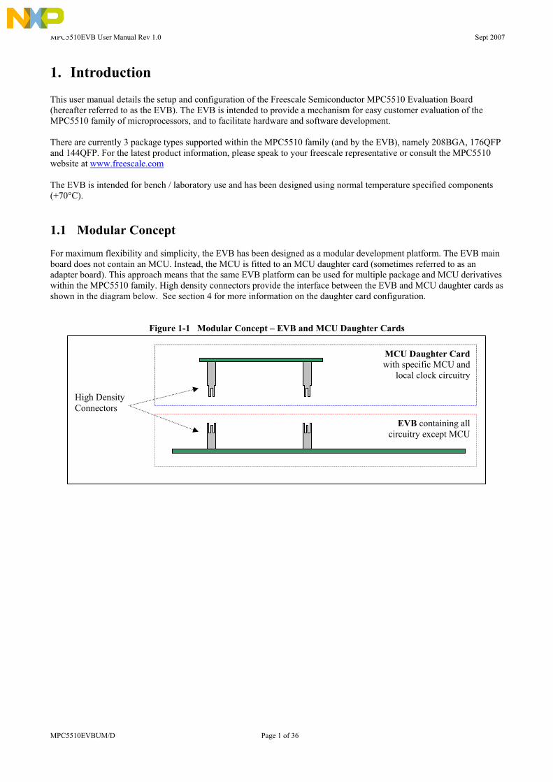
1. Introduction This user manual details the setup and configuration of the Freescale Semiconductor MPC5510 Evaluation Board (hereafter referred to as the EVB). The EVB is intended to provide a mechanism for easy customer evaluation of the MPC5510 family of microprocessors, and to facilitate hardware and software development. There are currently 3 package types supported within the MPC5510 family (and by the EVB), namely 208BGA, 176QFP and 144QFP. For the latest product information, please speak to your freescale representative or consult the MPC5510 website at www.freescale.com The EVB is intended for bench / laboratory use and has been designed using normal temperature specified components (+70°C). 1.1 Modular Concept For maximum flexibility and simplicity, the EVB has been designed as a modular development platform. The EVB main board does not contain an MCU. Instead, the MCU is fitted to an MCU daughter card (sometimes referred to as an adapter board). This approach means that the same EVB platform can be used for multiple package and MCU derivatives within the MPC5510 family. High density connectors provide the interface between the EVB and MCU daughter cards as shown in the diagram below. See section 4 for more information on the daughter card configuration.
Figure 1-1 Modular Concept – EVB and MCU Daughter Cards
MCU Daughter Card with specific MCU and
local clock circuitry
EVB containing all circuitry except MCU
High Density Connectors

MPC5510EVB User Manual Rev 1.0 Sept 2007
MPC5510EVBUM/D Page 2 of 36
•
• ” headers via a Philips high speed CAN transceiver (The
• pe area.
d VRL. •
nted as 2mm pitch whereas eaders are 0.1inch (2.54mm). This prevents inadvertently fitting a jumper to a header.
2. EVB Features The EVB provides the following key features:
• Support provided for different MPC5510 MCU family members by utilising MCU daughter cards. • Single 12-14V external power supply input with on-board regulators to provide all of the necessary EVB and
MCU voltages. Power may be supplied to the EVB via a 2.1mm barrel style power jack or a 2-way lever connector. 12V operation allows in-car use if desired.
• Freescale System Basis Chip footprint to allow use of the SBC power supply if required (available end 2007). • Flexible on-board power supply configuration with the option to bypass the internal MCU regulators for
diagnostic purposes. MCU power can also be sourced from either the EVB regulators or the SBC. • Master power switch and regulator status LED’s. • User reset switch with status LED’s. • User configurable LVI (Low Voltage Inhibit) device to monitor the status of the 5V regulators. • Control of the BOOTCFG status via a dedicated jumper. • Flexible MCU clocking options allow provision of an external clock via an SMA connector or 8Mhz EVB clock
oscillator circuit. Jumpers on the daughter card allow selection between these external clocks or the local onnector for easy access. daughter card ALC oscillator circuitry. The MCU clkout signal is routed to an SMA c
• Standard 14-pin ONCE debug connector and 38-pin MICTOR Nexus2+ connectors. • Twin 120-way polarised daughter card expansion connectors allowing connection of the MCU daughter card or
a custom board for additional application specific circuitry. • All of the MCU signals are readily accessible at a group of port-ordered 0.1” pitch headers. • Up to 256Kbytes of external SRAM memory which can be configured as either 32-bit or 16-bit data port width.
SCI channels A and B can be routed to either a standard DB9 female connector (PC RS-232 compliant) or LINinterface header (0.1”), both will full physical transceivers (the SBC provides an additional 2 LIN interfaces). MCU FlexCAN channels A and C can be routed to 0.1SBC provides an additional CAN physical interface).
• 7x5 LED dot matrix display connected to the MCU eMIOS PWM channel [0..11] via a 16244 buffer / driver. User prototyping area consisting of a 0.1” grid of through hole pads with easy access to the EVB ground and power supply rails. 4 active low LED’s and 4 small pushbutton switches are adjacent to the prototy
• Jumper selectable variable resistor connected to ATD channel 0, driving between VRH an Liberal scattering of GND test points (surface mount loops) placed throughout the EVB.
Note – to alleviate confusion between jumpers and headers, all EVB jumpers are implemeh
IMPORTANT Before the EVB is used or power is applied, please fully read this user manual.
Failure to correctly configure the board may cause irreparable component, MCU or EVB damage.

MPC5510EVB User Manual Rev 1.0 Sept 2007
MPC5510EVBUM/D Page 3 of 36
3. Configuration This section details the configuration of each of the EVB functional blocks. Throughout this document, all of the default jumper and switch settings are clearly marked with “(D)” and are shown in blue text. This should allow a more rapid return to the default state of the EVB if required. Note that the default configuration for 3-way jumpers is a header fitted between pins 1 and 2. On the EVB, 2-way and 3-way jumpers have been aligned such that Pin1 is either to the top or to the left of the jumper. On 2-way jumpers, the source of the signal is connected to Pin1. The EVB has been designed with ease of use in mind and has been segmented into functional blocks as shown below. Detailed silkscreen legend has been used throughout the board to identify all switches, jumpers and user connectors.
Flexray
Serial (SCI) LIN CAN
Prototype Area
User LEDs and switches
User Connectors
EIM and SRAM
Voltage Regulators
Daughter Card Connectors (with MCU Daughter Card
Superimposed)
JTAG and NEXUS
Clock Circuitry and SMA In / Out
Power Connectors
LED Matrix
Power Routing Jumpers
Reset and LVI
User Potentiometer
Figure 3-1 EVB Functional Blocks

MPC5510EVB User Manual Rev 1.0 Sept 2007
MPC5510EVBUM/D Page 4 of 36
TsbE
3.1 Power Supply Configuration The EVB requires an external power supply voltage of 12V DC, minimum 1A. This allowa vehicle if required. The 12v input is regulated on the EVB using 1 linear and 3 switchinnecessary EVB and MCU operating voltages of 5.0V, 3.3V and 1.5V. In addition, the EVSystem Basis Chip (SBC) which is an integrated regulator for the MCU power supply lindifferent power supply input connectors on the EVB as detailed below.
3.1.1 Power Supply Connectors 2.1mm Barrel Connector – P28: This connector should be used to connect the supplied wall-plug mains adapter. Note – ifadapter is used, care must be taken to ensure the 2.1mm plug uses the correct polarisation
GND
V+ (12V)
Figure 3-2 2.1mm Power Connector
2-Way Lever Connector – P32: This can be used to connect a bare wire lead to the EVB, typically from a laboratory powthe connectors is clearly marked on the EVB. Care must be taken to ensure correct conne
GND
V+ (12V)
Figure 3-3 2-Lever Power Connector
3.1.2 Power Switch (SW6) Slide switch SW6 can be used to isolate the power supply input from the EVB voltage re
Moving the slide switch to the right (away from connector P32) will turn the EVMoving the slide switch to the left (towards connector P32) will turn the EVB o
he Power supply ection is located in the ottom left area of the VB
s the EVB to be easily used in g regulators to provide the B supports the Freescale es. For flexibility there are two
a replacement or alternative as shown below:
er supply. The polarisation of ction.
gulators if required.
B on. ff.

MPC5510EVB User Manual Rev 1.0 Sept 2007
MPC5510EVBUM/D Page 5 of 36
3.1.3 Regulator Power Jumpers (J42, J44, J45 and J46) The Power supply control jumpers are located adjacent to the respective regulators. As mentioned above, the EVB has four voltage regulators on board:
- 1.5V switching regulator (U20) to supply the MCU Core voltage when the MCU on-chip regulator is disabled. - 3.3V switching regulator (U21) for EVB peripherals and MCU logic when the on-chip regulator is disabled. - 5.0V switching regulator (U22) for the MCU regulator and I/O and EVB peripherals. - 5.0V linear regulator (U19) for the MCU ADC power supply
All of the regulators have the option of being disabled if they are not required. The table below details the jumper configurations for enabling and disabling the regulators. By default, all of the regulators are enabled.
Table 3-1 Regulator Power Jumpers
Jumper Position PCB Legend Description FITTED (D) 5.0V linear regulator output is Enabled J42 (5.0V-LINEAR) REMOVED ENABLE 5.0V linear regulator output is Disabled FITTED 1.5V switching regulator output is Disabled J44 (1.5V) REMOVED (D) DISABLE 1.5V switching regulator output is Enabled FITTED 3.3V switching regulator output is Disabled
J45 (3.3V) REMOVED (D) DISABLE 3.3V switching regulator output is Enabled FITTED 5.0V switching regulator output is Disabled J46 (5.0V) REMOVED (D) DISABLE 5.0V switching regulator output is Enabled
3.1.4 Power Status LED’s and Fuse When power is applied to the EVB, four green LED’s adjacent to the voltage regulators show the presence of the supply voltages as follows: LED DS10 – Indicates that the 5.0V linear regulator is enabled and working correctly LED DS11 – Indicates that the 1.5V switching regulator is enabled and working correctly LED DS12 – Indicates that the 3.3V switching regulator is enabled and working correctly LED DS13 – Indicates that the 5.0V switching regulator is enabled and working correctly If no LED’s are illuminated when power is applied to the EVB and the regulators are correctly enabled using the appropriate jumpers, it is possible that either power switch SW6 is in the “OFF” position or that the fuse F1 has blown. The fuse will blow if power is applied to the EVB in reverse-bias, where a protection diode ensures that the main fuse blows rather than causing damage to the EVB circuitry. If the fuse has blown, check the polarity of your power supply connection then replace fuse F1 with a 20mm 500mA fast blow fuse.
3.1.5 SBC Power Jumper (J41) The optional SBC (System Basis Chip) regulator has a single power supply input jumper as detailed in the table below. By default, the SBC is disabled. For more details on the SBC regulator see Figure 3-4 below.
Table 3-2 SBC Power Jumpers
Jumper Position PCB Legend Description FITTED SBC linear regulator output is Enabled J41 (SBC-PWR) REMOVED (D) SBC linear regulator output is Disabled
Note – the SBC will not be available until the end of 2007 so it will not be fitted on an EVB manufactured prior to the SBC release date.

MPC5510EVB User Manual Rev 1.0 Sept 2007
MPC5510EVBUM/D Page 6 of 36
The MCU power supply
jumpers are located in the centre of the EVB in a box titled “MCU Supply”
3.1.6 MCU Supply Routing and Jumpers (J21, J25, J27, J29, J30, J33, J34, J36, J37, J38)
The MCU has internal regulators to generate the 3.3V and 1.5V supplies for VDDSYN, VDD33 and VDD. Whilst this is the intended mode of operation for the MCU, the EVB allows the internal MCU regulators to be disabled by disconnecting VDDR and applying external voltages to the VDDSYN, VDD33 and VDD pins via jumpers J25, J27 and J21 respectively). The VDDE[1..3] pins control the pad voltages over 3 groupings of pads (see the MCU reference manual for details). Jumpers J29, J30, J33 and J34 allow the VDDEx pins to be connected to the 5.0v or 3.3V switching regulators or to the SBC auxiliary output which can is software selectable between 5.0V and 3.3V. Each of the main supply pins (VDDA, VDDR, VPP and VDDEx) has the option of being routed from either the EVB regulators (where VDDA has a dedicated linear regulator to ensure a accuracy) or from the SBC.
Figure 3-4 Power Supply Routing
MCU Power
5V Switcher
3.3V Switcher
1.5V Switcher
5V Linear
12V
VDD (1.5)
VDD33
VDDSYN
VDDE1
(3.3v / 5v)
VPP
VDDR
VDDA
VDDE2
VDDE3
SBC
AUX
CAN Supply
MAIN
5v
5v
J38
J37
J36
J33
J30
J29
J25
J27
J21
J34
1
1
1
1
1
1
1

MPC5510EVB User Manual Rev 1.0 Sept 2007
MPC5510EVBUM/D Page 7 of 36
Table 3-3 MCU Power Supply Jumpers
Power Domain
Jumper Position PCB Legend
Description
1-2 (D) 5V-L MCU VDDA is powered from 5V linear regulator J38 (VDDA)
2-3 SBC MCU VDDA is powered from SBC (VDD output) 1-2 (D) 5V-S MCU internal VREG is powered from 5.0V switching reg 2-3 SBC MCU internal VREG is powered from SBC (VDD output) J37 (VDDR) * REMOVED* MCU regulator is not powered (See note below) 1-2 (D) 5V-S MCU VPP is powered from 5.0V switching regulator
5.0V
J36 (VPP) 2-3 SBC MCU VPP is powered from SBC (VCAN output)
1-2 (D) 5V-S VDDEx jumpers are supplied from 5V switching regulator J34 (VDDE SEL) 2-3 SBC VDDEx jumpers are supplied from SBC (VAUX Output)
1-2 (D) FRM J34 MCU VDDE1 is powered from output of J34 J33 (VDDE1) 2-3 3.3V MCU VDDE1 is powered from 3.3V switching regulator
1-2 (D) FRM J34 MCU VDDE2 is powered from output of J34 J30 (VDDE2) 2-3 3.3V MCU VDDE2 is powered from 3.3V switching regulator
1-2 (D) FRM J34 MCU VDDE3 is powered from output of J34
5.0V / 3.3V
J29 (VDDE3) 2-3 3.3V MCU VDDE3 is powered from 3.3V switching regulator
FITTED MCU VDD33 pin is powered from switching regulator J27 (VDD33) REMOVED (D) MCU VDD33 pin is not powered externally
FITTED MCU VDDSYN pin is powered from switching regulator 3.3V J25 (VDDSYN) REMOVED (D) MCU VDDSYN pin is not powered externally
FITTED MCU VDD pin is powered from 1.5v switching regulator 1.5V J21 (VDD15)
REMOVED (D) MCU VDD pin is not powered externally The jumper configuration shown in Table 3-3, details the default state of the EVB. In this configuration, the SBC is not used and all power is supplied from the Linear and Switching regulators.
- VDDA is connected to the 5.0V Linear regulator - VDDR is connected to the 5.0V switching regulator, enabling the internal MCU 3.3V / 1.5V regulators - VPP and VDDE[1..3] are connected to the 5.0V switching regulator - VDD33, VDDSYN and VDD are not powered externally.
IMPORTANT
When jumper J37 (VDDR) is in position 1-2 (5V-S), the MCU internal voltage regulators are enabled and supply power to the 3.3V and 1.5V MCU power domains. In this case, jumpers J27 (VDD33), J25 (VDDSYN) and J21 (VDD15) must not be fitted. Similarly, when jumper J37 is removed, no power is supplied to the MCU internal voltage regulators and jumpers J27 (VDD33), J25 (VDDSYN) and J21 (VDD15) must be fitted to power the respective MCU pins. The 3.3V and 1.5v switching regulators must also be enabled in this case. When the internal voltage regulator is disabled and power is applied to VDDSYN, VDD33 and VDD, a ferrite bead on VSSSYN needs to be activated. This is achieved by de-soldering a zero-ohm link on the bottom of the daughter card. See section 4.2.1 for details. Note that external regulator mode is not the intended mode of operation of the MCU and should be used for test purposes only.

MPC5510EVB User Manual Rev 1.0 Sept 2007
MPC5510EVBUM/D Page 8 of 36
3.1.6.1 VDDE[1..3] Voltage Groupings Before changing the VDDEx voltage from the default 5.0V setting, you need to ensure that this will not impact any of the EVB peripherals that may be in use. The table below details what EVB peripherals are tied to a particular VDDEx grouping and also the MCU pin operating voltage suitable for that peripheral.
Table 3-4 VDDE[1..3] Pad Groupings
Item Port Pins VDDE Group Required Pad Voltage LED Dot Matrix Display PortC[0..11] VDDE1 5.0V or 3.3V
External Memory
PortG[0..15], PortF[0..15], PortH[14,15], PortJ[0..7]
VDDE2 VDDE2 / 3 VDDE2 VDDE2
5.0V
CANA and CANC PortD [0..5] VDDE1 5.0V SCI / LIN A and B PortD[6..9] VDDE1 5.0V Flexray PortC[0..2, 7..9] VDDE1 5.0V or 3.3V (J18 selects) JTAG VDDE3 5.0V Nexus PF[0..11] VDDE2 / 3 5.0V
3.1.7 EVB Circuitry Power Domains Before disabling any of the EVB regulators, it is worthwhile considering if any of the EVB components or peripherals you require will be affected. Table 3-5 details a list of the various EVB components and peripherals powered by the regulators. Note – the SBC powers the MCU only and does not supply power to any of the EVB circuitry.
Table 3-5 Power Supply Distribution
Regulator Used On
1.5V (Switcher)
MCU VDD1.5 pins (ONLY use when on-chip MCU regulator is disabled) Daughter Card Connectors (1.5V) 1.5V Power section of Prototype area
3.3V (Switcher)
MCU VDD33 and VDDSYN pins (ONLY use when on-chip MCU regulator is disabled) MCU VDDEx pins (when run in 3.3v mode) Oscillator Module (Y1) GAL22V10 (EIM Control) Driver chip for LED Matrix I/O supply for Flexray interface when VIO is 3.3V Daughter Card Connectors (3.3V) 3.3V Power section of Prototype area
5.0V (Switcher)
MCU VDDEx (5v mode), VPP and VDDR pins LVI circuit main power (affecting Reset Switch) Reset-In / Reset-Out logic Reset configuration circuitry SRAM memory and address latches RS-232 Transceiver LIN transceiver CAN transceivers Flexray transceivers EIM signal pullup resistors Daughter Card Connectors (5.0V) 5.0V Power section of Prototype area eICE and Nexus connectors
5.0V (Linear)
MCU VDDA pin LVI circuit monitor
MPC5510EVB User Manual Rev 1.0 Sept 2007
MPC5510EVBUM/D Page 9 of 36
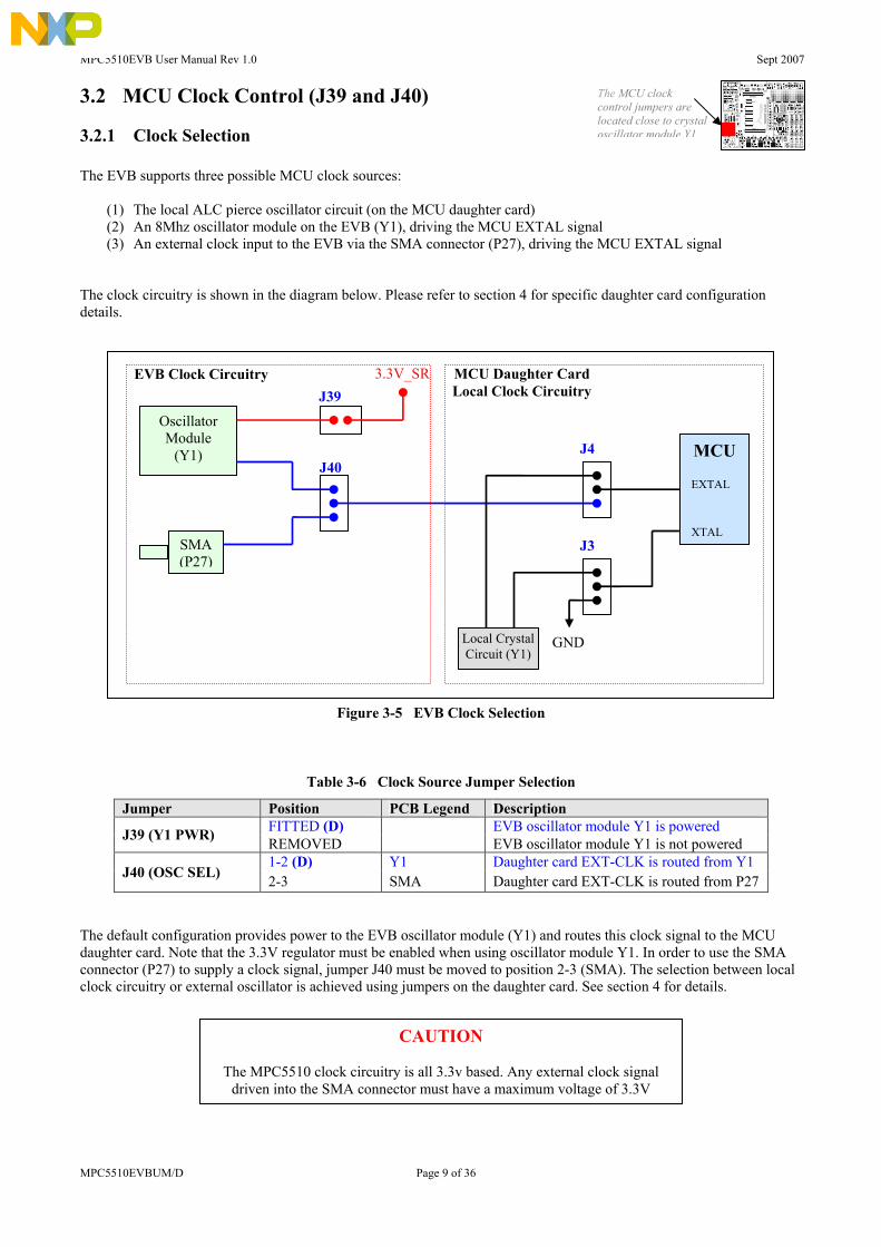
The MCU clock control jumpers are located close to crystal oscillator module Y1.
3.2 MCU Clock Control (J39 and J40)
3.2.1 Clock Selection The EVB supports three possible MCU clock sources:
(1) The local ALC pierce oscillator circuit (on the MCU daughter card) (2) An 8Mhz oscillator module on the EVB (Y1), driving the MCU EXTAL signal (3) An external clock input to the EVB via the SMA connector (P27), driving the MCU EXTAL signal
The clock circuitry is shown in the diagram below. Please refer to section 4 for specific daughter card configuration details.
J39
SMA (P27)
Oscillator Module
(Y1)
3.3V_SR
Figure 3-5 EVB Clock Selection
Table 3-6 Clock Source Jumper Selection
Jumper Position PCB Legend Description FITTED (D) EVB oscillator module Y1 is powered J39 (Y1 PWR) REMOVED EVB oscillator module Y1 is not powered 1-2 (D) Y1 Daughter card EXT-CLK is routed from Y1
J40 (OSC SEL) 2-3 SMA Daughter card EXT-CLK is routed from P27 The default configuration provides power to the EVB oscillator module (Y1) and routes this clock signal to the MCU daughter card. Note that the 3.3V regulator must be enabled when using oscillator module Y1. In order to use the SMA connector (P27) to supply a clock signal, jumper J40 must be moved to position 2-3 (SMA). The selection between local clock circuitry or external oscillator is achieved using jumpers on the daughter card. See section 4 for details.
Local Crystal Circuit (Y1)
MCU EXTAL XTAL
MCU Daughter Card Local Clock Circuitry
J40 J4
J3
GND
EVB Clock Circuitry
CAUTION
The MPC5510 clock circuitry is all 3.3v based. Any external clock signal
driven into the SMA connector must have a maximum voltage of 3.3V

MPC5510EVB User Manual Rev 1.0 Sept 2007
MPC5510EVBUM/D Page 10 of 36
The RESET switch (RED) and LVI circuitry is located in the top left corner of the EVB in the area titled “RESET “
3.3 Reset Control (Jumpers J17, J19, J20, SW1) The EVB incorporates an LVI (Low Voltage Inhibit) device to provide under-voltage protection for the two main 5.0V regulators (Linear and Switcher). The SBC has its on monitoring circuit so does not require external monitoring. When either of the 5.0V regulator voltages fall below a preset threshold level, the LVI will assert the MCU reset line to prevent incorrect operation of the MCU (or EVB circuitry). The table below shows the approximate threshold voltages for each regulator
Table 3-7 LVI Monitor Threshold Voltages
Regulator Minimum Voltage Before MCU reset 5.0V Linear 4.45V
5.0V Switcher 4.65V The LVI is powered from the 5.0V switching regulator and monitors the 5.0V linear using a 2nd power fail monitor circuit. The LVI also provides a de-bounced input for EVB reset switch SW1. Jumpers are provided to disable either the main LVI reset out (which affects the reset from the 5.0V switching regulator and from the reset switch) or the power fail out circuit (which only affects the reset from the 5.0V linear regulator). If the switching regulator LVI is disabled, the reset switch will not function.
Table 3-8 LVI Control Jumpers
Jumper Position PCB Legend Description FITTED (D) 5.0V switching regulator is monitored, Reset switch active J20
Posn 1-2 REMOVED MAIN 5.0V switching regulator is not monitored, Reset switch inactive
FITTED (D) 5.0V linear regulator is monitored J20 Posn 3-4 REMOVED LINEAR 5.0V linear regulator is not monitored
Notes:
- If the 5.0V switching regulator is disabled for any reason, the LVI circuit will attempt to assert the MCU Reset signal. Jumper shunts on jumper J20 position 1-2 and 3-4 must be removed in this situation. This will also leave the reset switch SW1 inoperative.
- If the 5.0V linear regulator is disabled, the shunt on jumper J20 position 3-4 must be removed to prevent the LVI asserting reset.
3.3.1 Reset LEDs There are two reset LED’s, DS1 (AMBER) and DS2 (RED), placed adjacent to the EVB RESET switch to indicate the RESET status of the EVB and MCU. LED DS2, titled “RST”, will illuminate if the MCU itself issues a reset. In this condition, LED DS1 will not illuminate. LED DS1, titled “USR”, will illuminate when one of the following external hardware devices issues a reset to the MCU:
- LVI circuitry (either an under-voltage detection or the reset switch is pressed). - There is a reset being asserted from the user connectors or from the daughter card. - There is a reset being driven from the Nexus or JTAG debug probe. Note that LED DS2 (MCU Reset) will also illuminate during an external (user) reset!

MPC5510EVB User Manual Rev 1.0 Sept 2007
MPC5510EVBUM/D Page 11 of 36
3.3.2 Reset Buffering Scheme The MPC5510 family has a single reset pin. This single pin functions as a dual purpose input / output signal, providing Reset-In and Reset-Out functionality. There is a lot of circuitry on the EVB that has access to the reset pin. In order to reduce the loading on the MCU when driving the reset pin and also to allow connection of non open-drain reset inputs, a reset-in and reset-out buffering scheme is implemented as shown in Figure 3-6. Reset-In - There are 3 possible external sources of reset:
- JTAG / Nexus connector reset - User reset (from user connectors) - LVI reset circuitry, including the reset switch.
Each of these reset sources is fed into the input of an AND gate and then converted to an open-drain output which is directly connected to the MCU reset pin.
Reset-Out - The MCU reset pin is buffered to provide a reset-out signal, capable of driving the reset LED and also all other devices requiring a reset input. The reset buffering scheme is detailed below – note that the SBC also has an open drain reset in / out that is connected directly to the MCU reset line.
MCU RESET
Figure 3-6 EVB Reset Buffering Scheme
Jumper J17 is used to completely disconnect the reset-in buffering if desired. This is for debug purposes only and should normally be left connected. Disconnecting this jumper will mean no external MCU reset can be achieved
Table 3-9 Reset-Out Control Jumper
Jumper Position PCB Legend Description
FITTED (D) External reset source (LVI, Debug or Target) will be able to assert MCU reset J17 (RST-IN)
REMOVED
External reset is disabled (Not recommended)
Reset OUT
From TGT
From JTAG / Nexus
From LVI (Main)
GND
Tri State Buffer
Reset IN
From LVI (Linear)
J20
J17
(To RED Reset LED, BDM Reset In, external device reset)
Reset OUT

MPC5510EVB User Manual Rev 1.0 Sept 2007
MPC5510EVBUM/D Page 12 of 36
3.3.3 Reset Boot Configuration (J19) The MPC5510 has a single boot configuration pin (BOOTCFG) which determines the boot location of the MCU based on the state of the pin at POR (Power On Reset). This is shown in the table below:
Table 3-10 BOOTCFG Control
Jumper Position PCB Legend Description 1-2 (D) FSH MCU boots from internal flash J19 (BOOT CFG) 2-3 SERIAL MCU boots from external serial source
Note – there have been some problems observed when application code is present in flash and an attempt is made to load and execute a different application from internal RAM. Depending on the configuration and speed of the debugger used, it is feasible that the application code in flash will already have started to execute by the time the debugger gains control. This has implications if the flash code has already done some configuration of the device that is in conflict with the operation of the code that is about to be loaded into RAM. To prevent this occurring, it is advised to either erase the internal flash or to prevent the MCU booting from flash by moving jumper J19 to position 2-3.
The ONCE and NEXUS connectors are located at the left hand edge of the EVB
3.4 Debug Configuration (J24, J28, J31, J31B)
The EVB supports a standard ONCE cable with a 14-pin 0.1” walled header footprint. There is also a 38-pin MICTOR connector for Nexus 2+ debug. Four generic jumpers are associated with both the ONCE and Nexus, as detailed below.
3.4.1 TCLK Configuration Some debug manufacturers specify whether the debug TCLK signal is pulled low or high. Jumper J28 provides the ability to select whether TCLK is pulled to GND or 5V.
Table 3-11 ONCE / NEXUS TCLK Termination Control
Jumper Position PCB Legend Description 1-2 (D) 5V TCLK signal is pulled to 5.0V via 10KΩ J28
(TCLK PULL) 2-3 GND TCLK signal is pulled to GND via 10KΩ Notes:
- J28 is located to the right of the reset switch, out-with the ONCE / Nexus connector area. - To achieve accurate low power current measurements, TCLK should be pulled to GND
3.4.2 Reset Buffering Most debug probes only assert the MCU reset line but some also have the ability to also monitor the status of the reset line. This is not possible when the reset signal is buffered so jumper J31 is included to allow routing the debug reset signal direct to the MCU reset pin or via the EVB Reset-In buffering.
Table 3-12 JTAG / NEXUS Target Reset Routing
Jumper Position PCB Legend Description
1-2 (D) BUFFER JTAG reset signal is buffered to MCU RESET pin (connected to the MCU Reset-In circuitry) J31 (JRST)
2-3 DIRECT JTAG reset signal is connected direct to MCU RESET pin The default configuration connects the JTAG reset signal to the MCU reset via a buffer so the probe cannot monitor the reset. If your debug probe has an open-drain reset capable of monitoring the reset signal, this can be enabled by moving jumper J31 to position 2-3.

MPC5510EVB User Manual Rev 1.0 Sept 2007
MPC5510EVBUM/D Page 13 of 36
CAUTION
If jumper J31 is positioned 2-3 and the debug probe actively drives the reset line high and low, nothing else will be able to assert the MCU reset (including the MCU itself).
3.4.3 PFO Selection MCU pin PF0 has alternate functions of EVTI (debug control signal) and R/W. To prevent conflicts between the external memory and debug interface, jumper J31B is used to route PF0 to either the debug connectors or the external memory as shown in the table, below.
Table 3-13 PFO EVTI / R/W Function Selection
Jumper Position PCB Legend Description 1-2 (D) EVTI MCU PFO is routed to the ONCE / Nexus debug connector J31B (PFO Sel) 2-3 RW MCU PFO is routed to the external memory system
The default configuration connects PF0 to the debug connectors to act as EVTI. If the external bus is to be used then J31B must be moved to position 2-3 to route PF0 to the memory subsystem as the R/W signal. Note – EVTI is optional for ONCE debug and generally not required so with the jumper configured in position 2-3 to enable RW, a “ONCE” debug session can still be established.
3.4.4 Vendor I/O Configuration Some Nexus debug probes can use the “Vendor I/O2” signal to drive BOOTCFG reset configuration data at reset. The EVB is designed such that this will over-ride any BOOTCFG data supplied by jumper J19 (see section 3.3.3). A jumper is supplied to allow this feature to be enabled if desired.
Table 3-14 Vendor I/O2 Drive Control
Jumper Position PCB Legend Description FITTED Vendor I/O2 pin disconnected J24
(VEND-IO) REMOVED (D) Vendor I/O2 pin can drive BOOTCFG at reset By default, the debug tool will not have the ability to over-ride the EVB BOOTCFG settings and J24 will be removed. To enable this feature, fit jumper J24. Note – Be careful when fitting jumper J24 as this will override the EVB BOOTCFG setting when a nexus probe is fitted to the EVB.

MPC5510EVB User Manual Rev 1.0 Sept 2007
MPC5510EVBUM/D Page 14 of 36
3.4.5 Debug Connector Pinouts The EVB is fitted with 14-pin JTAG / ONCE and 38-pin Nexus 2+ debug connectors. The following diagram shows the 14-pin JTAG / ONCE connector pinout (0.1” keyed header).
VSS
VSS
VSS
N/C
TMS
VSS
JCOMP
TDI
TDO
TCLK
EVTI
RESET
VDD5V
RDY
1
3
5
7
9
11
13
2
4
6
8
10
12
14
Figure 3-7 MPC5510 JTAG / ONCE Connector
The Nexus module used on the MPC5510 family uses the JTAG pins (for control of the Nexus block) along with additional Nexus pins for trace messages. Nexus mode is entered by a JTAG sequence whereby the Nexus EVTI pin is sampled on the rising edge of the JTAG TRST pin. If the EVTI is asserted on TRST, Nexus is enabled. The table below shows the pinout of the 38-pin MICTOR Nexus connector for the MPC5510
Table 3-15 NEXUS Debug Connector Pinout
Pin No Function Connection Pin No Function Connection 1 Reserved --- 2 Reserved --- 3 Reserved --- 4 Reserved --- 5 Vendor I/O-0 --- 6 CLKOUT MCU PE6 7 Vendor I/O-2 BOOTCFG 8 Vendor I/O-3 --- 9 Reset-In Reset CCT 10 EVTI MCU PF0
11 TDO MCU TDO 12 VREF P5V 13 Vendor I/O-4 --- 14 RDY --- 15 TCLK MCU TCK 16 MDO[7] MCU PF11 17 TMS MCU TMS 18 MDO[6] MCU PF10 19 TDI MCU TDI 20 MDO[5] MCU PF9 21 TRST JCOMP 22 MDO[4] MCU PF8 23 Vendor I/O-1 --- 24 MDO[3] MCU PF7 25 Tool I/O-3 RST-OUT 26 MDO[2] MCU PF6 27 Tool I/O-2 --- 28 MDO[1] MCU PF5 29 Tool I/O-1 --- 30 MDO[0] MCU PF4 31 UBATT 12V Vin 32 EVTO MCU PF1 33 UBATT 12V Vin 34 MCK0 MCU PF3 35 Tool I/O-0 --- 36 MSE1 ---- 37 VALTREF P5V
38 MSEO MCU PF2 Note - In order to preserve the ability to accurately measure power consumption on the MCU pins, the JTAG and Nexus connector reference voltages are sourced directly from the 5V regulator or from the 12V unregulated input.

MPC5510EVB User Manual Rev 1.0 Sept 2007
MPC5510EVBUM/D Page 15 of 36
The external memory block is located on the right had side of EVB with some jumpers to right of the reset switch
3.5 External Memory Configuration The MPC5510 external bus interface supports a multiplexed address/data bus with a configurable data-port size of either 16-bits or 32-bits. The EVB uses 3 x 128Kbyte (16-bit) asynchronous SRAM memories to provide either 128Kbytes of memory in 16-bit port width mode or 256Kbytes of memory in 32-bit port width. A high speed PLD is used to control the routing of the relevant control signals depending on the selected port size. Note that the SRAM does not supply a transfer acknowledge (TA) signal to the MCU at the end of a data cycle so the MCU external bus must be configured with auto TA acknowledge enabled. Additional wait states may be required depending on the MCU bus speed. See the relevant MCU reference manual for more details.
MPC5516
SRAM 64Kx16 (Upper)
Address Latch
(Upper)
Address Latch
(Lower)
Mux’d Address/Data
Demux’d Address
Data (Effectively)
Naming Conventions: Address A31 is LSB Data D31 is LSB
SRAM 64Kx16 (Lower)
SARAM 64Kx16
D[0..15]
D[16..31]
A[13..29]
A[13..29]
A[15..30]
D[16..31]
32-bit Port
16-bit Port
Figure 3-8 External Memory Subsystem
The MPC5510 family does not have an “expanded mode” of operation unlike other MCU families you may have encountered. Instead the individual port pins must be switched to the correct mode of operation for the external bus. The table below shows what MCU pins are required for correct bus operation in 16-bit and 32-bit port size modes.
Table 3-16 MCU pins required for EIM SRAM operation
SRAM Port Size Configuraiton
PortE Port F Port G Port H Port J
16-Bit 6 0, 1, 9, 10, 11, 12, 13, 14, 15 [0..15] 32-Bit 6 [0..15] [0..15] 14, 15 [0..7]
Notes:
- PE6 is the MCU CLKOUT pin which is required for the operation of the external memory - PortF is shared with the Nexus debug port so the external memory cannot be used at the same time as Nexus.
Jumpers are provided as detailed in the following sections to enable the memory system and also to control the MCU chip select assignment and port size configuration. Note that the 3.3V and 5.0V switching regulators must be enabled for the external memory system to function.
MPC5510EVB User Manual Rev 1.0 Sept 2007
MPC5510EVBUM/D Page 16 of 36
3.5.1 Memory Power Control (J22, J32)) The memory subsystem has components operating at 3.3V and 5.0V. Each of these power domains has a separate power jumper as detailed below. The SRAM devices and address latch buffers operate at 5.0V, controlled by jumper J22. The PLD used to control the logic is powered from 3.3V (with 5.0V tolerant I/O). This has a separate power jumper J32.
Table 3-17 SRAM, and PLD Power Control Jumpers (J22, J32)
Jumper Position PCB Legend Description FITTED (D) The SRAM and address latches are powered (enabled) J22
(SRAM PWR) REMOVED The SRAM and latches are not powered (disabled) FITTED The control PLD is powered (enabled) J32
(GAL-PWR) REMOVED (D) The control PLD is not powered (disabled) By default the SRAM memory and latches are powered but the PLD is disabled. This ensures that outputs on the buffers and SRAM’s are tri-stated so do not affect the corresponding GPIO signals. To power down the memory and latches if desired, remove jumper J22. In order to use the external SRAM, the memory, latches and GAL must all be powered by fitting jumpers J22 and J32. Note – The SRAM and buffers are 5.0V devices so the corresponding MCU pins must be configured as 5.0V.
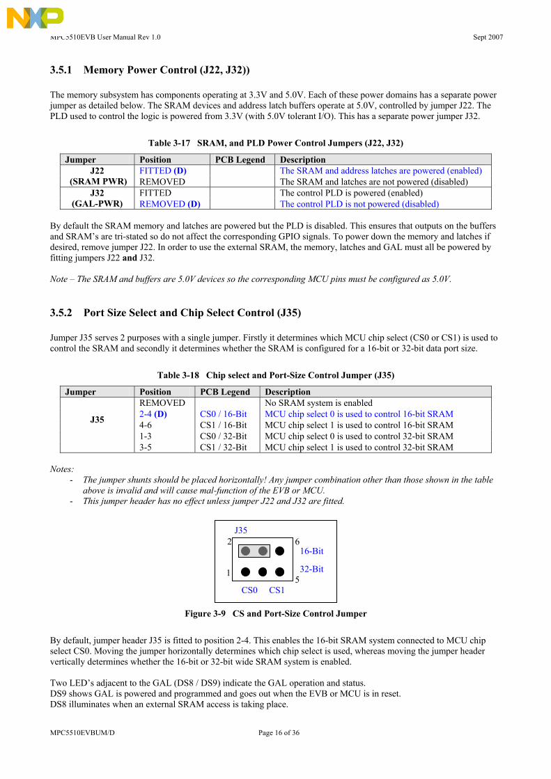
3.5.2 Port Size Select and Chip Select Control (J35) Jumper J35 serves 2 purposes with a single jumper. Firstly it determines which MCU chip select (CS0 or CS1) is used to control the SRAM and secondly it determines whether the SRAM is configured for a 16-bit or 32-bit data port size.
Table 3-18 Chip select and Port-Size Control Jumper (J35)
Jumper Position PCB Legend Description REMOVED No SRAM system is enabled 2-4 (D) CS0 / 16-Bit MCU chip select 0 is used to control 16-bit SRAM 4-6 CS1 / 16-Bit MCU chip select 1 is used to control 16-bit SRAM 1-3 CS0 / 32-Bit MCU chip select 0 is used to control 32-bit SRAM
J35
3-5 CS1 / 32-Bit MCU chip select 1 is used to control 32-bit SRAM Notes:
- The jumper shunts should be placed horizontally! Any jumper combination other than those shown in the table above is invalid and will cause mal-function of the EVB or MCU.
- This jumper header has no effect unless jumper J22 and J32 are fitted.
J35
CS0 CS1
16-Bit
32-Bit
2 6
1 5
Figure 3-9 CS and Port-Size Control Jumper
By default, jumper header J35 is fitted to position 2-4. This enables the 16-bit SRAM system connected to MCU chip select CS0. Moving the jumper horizontally determines which chip select is used, whereas moving the jumper header vertically determines whether the 16-bit or 32-bit wide SRAM system is enabled. Two LED’s adjacent to the GAL (DS8 / DS9) indicate the GAL operation and status. DS9 shows GAL is powered and programmed and goes out when the EVB or MCU is in reset. DS8 illuminates when an external SRAM access is taking place.

MPC5510EVB User Manual Rev 1.0 Sept 2007
MPC5510EVBUM/D Page 17 of 36
The CAN section is located in the top right corner of the EVB in an area marked “CAN”
3.6 CAN Configuration (J3, J4, J7) The EVB has a Philips PCA82C250T high speed CAN transceiver on each of the MCU CAN-A and CAN-C channels. The transceiver is pre-configured for high speed operation by tying pin 8 of each PCA82C250T to ground via a zero ohm resistor. If required, these resistors can be exchanged to provide slope control mode of operation. See the EVB schematics at the end of this manual for details on the resistor to change. For flexibility, the CAN transceiver I/O is connected to a standard 0.1” connector at the top edge of the PCB. Connector P3 provides the CAN bus level signal interface for CAN-A and connector P4 for CAN-B. The pinout for these connectors is shown below.
HI LOW GND
1
Figure 3-10 CAN Physical Interface Connector
Each of the MCU signals to the CAN transceivers is jumpered, allowing the transceiver to be isolated if the respective MCU pin is not configured or used for CAN operation. There is a 2x2 jumper for each CAN channel (one for Rx, one for Tx), as shown in the table below. The Global power jumper (J7) physically removes power from both CAN transceivers.
Table 3-19 CAN Control Jumpers (J3, J4, J7)
Jumper Position PCB Legend Description FITTED (D) Power is applied to both CAN transceivers J7
(VDD-CAN) REMOVED No power is applied to CAN transceivers
FITTED (D) MCU CNTX-A is connected to CAN controller A J3 (CAN-A) Posn 1-2 REMOVED TX MCU CNTX-A is NOT routed to CAN controller .
FITTED (D) MCU CNRX-A is connected to CAN controller A J3 (CAN-A) Posn 3-4 REMOVED RX MCU CNRX-A is NOT routed to CAN controller.
FITTED (D) MCU CNTX-C is connected to CAN controller C J4 (CAN-C) Posn 1-2 REMOVED TX MCU CNTX-C is NOT routed to CAN controller .
FITTED (D) MCU CNRX-C is connected to CAN controller C J4 (CAN-C) Posn 3-4 REMOVED RX MCU CNRX-C is NOT routed to CAN controller.
The default configuration is with all jumpers fitted. This fully enables both CAN-A and CAN-C, with all MCU signals routed to the transceivers. If the MCU is configured such that a CAN channel is used as GPIO, then the respective jumpers must be removed from J3 or J4 or conflicts will occur. Notes
- Both CAN channels are available on all current package derivatives (see table below) - Care should be taken when fitting the jumper headers to the 2x2 jumper blocks J3 and J4 as they can easily be
fitted in the incorrect orientation. Jumpers J3 and J4 are fitted horizontally.
Table 3-20 CAN Pin Availability
1ST Alternate Pin Availability CAN TX RX 144 Pin 176 Pin 208 Pin
A PD0 PD1 B PD3 PD2 C PD4 PD5

MPC5510EVB User Manual Rev 1.0 Sept 2007
MPC5510EVBUM/D Page 18 of 36
The RS232 circuitry is located at the top edge of the EVB in an area titled “SCI”
3.7 RS232 Configuration (J9, J10, J11) The EVB has a single MAX232CSE RS232 transceiver device, providing RS232 signal translation for MCU SCI channels A and B. Each of the two RS232 outputs from the MAX232 device is connected to a 9-way female D-Type connector, allowing a direct RS232 connection to a PC or terminal. Connector P5 provides the RS232 level interface for MCU SCI-A and P6 for MCU SCI-B. The pinout of these connectors is detailed below. Note that hardware flow control is not supported on this implementation.
Figure 3-11 RS232 Physical Interface Connector
The MPC5516 eSCI also provides hardware LIN master capability which is supported on the EVB via LIN transceivers (see section 3.8 for details). Jumpers J10 and J11 are provided to route the MCU SCI signals to either the RS232 or LIN physical interfaces as described below. There is also a global power jumper (J9) controlling the power to the RS232 transceivers.
Table 3-21 RS232 Control Jumpers Jumper Position PCB Legend Description
FITTED (D) Power is applied to the MAX232 transceiver J9 (SCI-PWR) REMOVED No power is applied to the MAX232 transceiver
2-4 (D) MCU TXD-A is routed via MAX232 to P5 4-6 MCU TXD-A is routed via LIN transceiver to P8 J10 (SCI-A)
Top Row REMOVED TXD
MCU TXD-A signal is disconnected from CAN/LIN 1-3 (D) MCU RXD-A is routed via MAX232 to P5 3-5 MCU RXD-A is routed via LIN transceiver to P8 J10 (SCI-A)
Bottom Row REMOVED
RXD MCU RXD-A signal is disconnected from CAN/LIN
2-4 (D) MCU TXD-B is routed via MAX232 to P6 4-6 MCU TXD-B is routed via LIN transceiver to P7 J11 (SCI-B)
Top Row REMOVED TXD
MCU TXD-B signal is disconnected from CAN/LIN 1-3 (D) MCU RXD-B is routed via MAX232 to P6 3-5 MCU RXD-B is routed via LIN transceiver to P7 J11 (SCI-B)
Bottom Row REMOVED RXD
MCU RXD-B signal is disconnected from CAN/LIN The default configuration enables SCI-A and SCI-B channels. RS232 compliant interfaces (with no hardware flow control) are available at DB9 connectors P5 and P6. If the MCU is configured such that the pins used on SCI-A or SCI-B are used for GPIO (see Table 3-22), then the relevant jumpers must be removed to avoid any conflicts occurring. If required, jumper J9 can be used to completely disable the SCI transceiver. Note - Care should be taken when fitting the jumper headers to the 2x3 jumper blocks J10 and J11 as they can easily be fitted in the incorrect orientation. Jumpers J10 and J11 are fitted horizontally.

MPC5510EVB User Manual Rev 1.0 Sept 2007
MPC5510EVBUM/D Page 19 of 36
Table 3-22 SCI Pin Availability
1ST Alternate Pin Availability SCI TX RX 144 Pin 176 Pin 208 Pin
A PD6 PD7 B PD8 PD9 C PF10 PF11 D PF12 PF13 E PH4 PH5 F PH6 PH7 G PB12 PB13 x h PB14 PB15 x
The LIN circuitry is located in the top edge of the EVB in an area titled “LIN”
3.8 LIN Configuration (J1, J2, J5, J6) The EVB is fitted with two freescale MC33399 LIN transceivers. The MCU SCI channels incorporate a hardware controlled LIN master, and as such, the LIN transceiver is connected to the same MCU pins as the RS232 transceiver. Jumpers J10 and J11 are used as described in section 3.7 (and in the table below) to determine whether the relevant MCU pins are connected to the LIN transceiver or the SCI transceiver. For flexibility, the LIN transceivers are connected to a standard 0.1” connector (P8 for LIN-A and P7 for LIN-B) at the top edge of the PCB as shown in the figure below. For ease of use, the 12V EVB supply is fed to pin1 of the connectors and the LIN transceiver power input to pin 2. This allows the LIN transceiver to be powered directly from the EVB supply by simply linking pins 1 and 2 of connector P7/P8 using a 0.1” jumper shunt.
LIN
P7/P8
1 VDD UNREG LIN VSUP
LIN
GND
Figure 3-12 LIN Physical Interface Connector
Along with the MCU signal routing jumpers (J10 / J11), there are jumpers (J5 / J6) to enable or disable the LIN transceiver and jumpers (J1 and J2) which determine if the LIN transceiver is operating in master or slave mode, as defined in the table below.

MPC5510EVB User Manual Rev 1.0 Sept 2007
MPC5510EVBUM/D Page 20 of 36
Table 3-23 LIN Control Jumpers
Jumper Position PCB Legend Description FITTED (D) LIN-B transceiver is configured for LIN Master mode J1
(LINB-M) REMOVED LIN-B transceiver is configured for LIN Slave mode FITTED (D) LIN-A transceiver is configured for LIN Master mode J2
(LINA-M) REMOVED LIN-A transceiver is configured for LIN Slave mode
FITTED (D) The LIN-B transceiver is enabled J5* (LINB-EN) REMOVED The LIN-B transceiver is disabled
FITTED (D) The LIN-A transceiver is enabled J6* (LINA-EN) REMOVED The LIN-A transceiver is disabled
2-4 (D) MCU TXD-A is routed via MAX232 to P5 4-6 MCU TXD-A is routed via LIN transceiver to P8 J10 (SCI-A)
Top Row REMOVED
TXD MCU TXD-A signal is disconnected from CAN/LIN
1-3 (D) MCU RXD-A is routed via MAX232 to P5 3-5 MCU RXD-A is routed via LIN transceiver to P8 J10 (SCI-A)
Bottom Row REMOVED RXD
MCU RXD-A signal is disconnected from CAN/LIN
2-4 (D) MCU TXD-B is routed via MAX232 to P6 4-6 MCU TXD-B is routed via LIN transceiver to P7 J11 (SCI-B)
Top Row REMOVED TXD
MCU TXD-B signal is disconnected from CAN/LIN 1-3 (D) MCU RXD-B is routed via MAX232 to P6 3-5 MCU RXD-B is routed via LIN transceiver to P7 J11 (SCI-B)
Bottom Row REMOVED RXD
MCU RXD-B signal is disconnected from CAN/LIN
* Note – Jumpers J5/J6 do NOT route power to LIN transceivers, they only control an enable line on the LIN device. Power to the LIN transceiver is supplied via connectors P7 / P8, pin 2. The Default LIN configuration is with the module enabled in master mode. By default, the EVB SCI/LIN signals are routed to the SCI transceivers. To use the LIN interface, the corresponding RX and TX pins must be routed to the LIN transceivers by re-configuring jumpers J10 and J11 with the shunts positioned on pins 2-3 and 5-6. LIN slave mode can be enabled by removing jumpers J1 / J2.
The Flexray circuitry is located in the top edge of the EVB in an area titled “Flexray”
3.9 Flexray Configuration (J12, J13, J14, J15, J16, J18)
The EVB is fitted with 2 flexray physical interfaces connected to MCU flexray channels A and B. Jumpers J12 and J14 are provided to route the respective MCU signals to the physical interfaces as described below.
Table 3-24 Flexray MCU Signal Routing Jumpers (J12, J14)
Jumper Position PCB Legend Description FITTED MCU PC1 is connected to Flexray A transceiver TX J12 (Flex-A)
Posn 1-2 REMOVED (D) TX MCU PC1 is not connected to Flexray A transceiver TX FITTED MCU PC0 is connected to Flexray A transceiver TXEN J12 (Flex-A)
Posn 3-4 REMOVED (D) TXEN MCU PC1 is not connected to Flexray A transceiver TXEN FITTED MCU PC2 is connected to Flexray A transceiver RXEN J12 (Flex-A)
Posn 5-6 REMOVED (D) RX MCU PC2 is not connected to Flexray A transceiver RXEN
FITTED MCU PC8 is connected to Flexray B transceiver TX J14 (Flex-A) Posn 1-2 REMOVED (D) TX MCU PC8 is not connected to Flexray B transceiver TX
FITTED MCU PC9 is connected to Flexray B transceiver TXEN J14 (Flex-A) Posn 3-4 REMOVED (D) TXEN MCU PC9 is not connected to Flexray B transceiver TXEN
FITTED MCU PC7 is connected to Flexray B transceiver RXEN J14(Flex-A) Posn 5-6 REMOVED (D) RX MCU PC7 is not connected to Flexray B transceiver RXEN

MPC5510EVB User Manual Rev 1.0 Sept 2007
MPC5510EVBUM/D
The power to the Flexray physical interface is controlled via jumper J16 to allow disconnection if required. The Flexray physical interface is capable of interfacing with MCU I/O voltages of 3.3V or 5.0V as defined by the voltage supplied to VIO via jumper J18. On the MPC5516, the MCU pad voltage is controlled by the voltage supplied to VDDE[1..3]. The user must ensure that the voltage on the respective PortC pads is the same as VIO supplied to the flexray interface.
Table 3-25 Flexray Power Control Jumpers (J16, J18)
Jumper Position PCB Legend Description FITTED 12V Flexray circuitry is powered from main 12Vinput J16 (Flex-PWR)
Posn 1-2 REMOVED (D) 12V 12V Flexray circuitry is not powered FITTED 5V Flexray circuitry is powered from 5.0V switching reg J16 (Flex-PWR)
Posn 3-4 REMOVED (D) 5V 5V Flexray circuitry is not powered FITTED VIO Flexray circuitry is powered from J18 J16 (Flex-PWR)
Posn 5-6 REMOVED (D) VIO VIO Flexray circuitry is not powered
1-2 (D) VIO is selected as 5.0V. 2-3 VIO is selected as 3.3V
J18 (VIO)
REMOVED
5V 3.3V
No Power is applied to the VIO jumper J16, posn 5-6 The flexray interface has 4 pins which are used for configuration and are pulled high or low controlled by a jumper as described in the table below. By default, all of the jumper headers are fitted. Please consult the Flexray physical interface specification before changing any of these jumpers.
Table 3-26 Flexray Control Jumpers (J13, J15)
Jumper Position PCB Legend Description FITTED (D) Flexray-A interface BGE signal is pulled to VIO J13 (Flex-A)
Posn 1-2 REMOVED BGE Flexray-A interface BGE signal is unterminated FITTED (D) Flexray-A interface EN signal is pulled to VIO J13 (Flex-A)
Posn 3-4 REMOVED EN Flexray-A interface EN signal is unterminated FITTED (D) Flexray-A interface STBN signal is pulled to VIO J13 (Flex-A)
Posn 5-6 REMOVED STBEN Flexray-A interface STBN signal is unterminated FITTED (D) Flexray-A interface WAKE signal is pulled to GND J13 (Flex-A)
Posn 7-8 REMOVED WAKE Flexray-A interface WAKE signal is unterminated
FITTED (D) Flexray-B interface BGE signal is pulled to VIO J15 (Flex-B) Posn 1-2 REMOVED BGE Flexray-B interface BGE signal is unterminated
FITTED (D) Flexray-B interface EN signal is pulled to VIO J15 (Flex-B) Posn 3-4 REMOVED EN Flexray-B interface EN signal is unterminated
FITTED (D) Flexray-B interface STBN signal is pulled to VIO J15 (Flex-B) Posn 5-6 REMOVED STBEN Flexray-B interface STBN signal is unterminated
FITTED (D) Flexray-B interface WAKE signal is pulled to GND J15 (Flex-B) Posn 7-8 REMOVED WAKE Flexray-B interface WAKE signal is unterminated
Notes:
- The default configuration has the flexray controller disabled. Flexray A and B are a second alternate function of PortC (as shown in the table below). Before enabling Flexray, you must ensure that none of the associated port pins are being used for any other function. On the EVB, PortC is shared with the LED Dot matrix display.
- The flexray physical interfaces use molex 1.25mm shrouded 2-pin connectors to connect to the flexray bus (as are standard fit on many Freescale development platforms using flexray).
A 40Mhz oscillator is required for the correan appropriate crystal is fitted to the MCU
Table 3-27
Flexray 2nd Alterna TXEN TX
A PC0 PC1 B PC9 PC8
Important: ct operation of the flexray controller. Please ensure that daughter card or use a 40Mhz external clock source.
Page 21 of 36
Flexray Pin Availability
te Pin Availability RX 144 Pin 176 Pin 208 Pin PC2 PC7

MPC5510EVB User Manual Rev 1.0 Sept 2007
MPC5510EVBUM/D Page 22 of 36
The LED matrix is located beneath the prototype area 3.10 LED Dot Matrix (J23)
The EVB includes a 5x7 LED dot matrix display connected via a 16244 buffer to MCU PortC / eMIOS [0..11] pins. The PWM ability on the pins allows strobing effects or the brightness of the matrix to be controlled if desired. The LED matrix does not have any automatic character generation circuitry so to generate characters, the 7 rows of the display must be written row at a time with sufficient scan speed to form the character without flicker. This is potentially a good background task for the Z0 core on the 5510! The diagram below shows how the matrix is connected. Note that this is a common anode display so is illuminated by asserting the columns “high” and the rows “low”. If desired, the top two rows can be disabled for use with GPIO leaving 5 rows enabled which is still sufficient for most characters.
Resistors to give approx 8mA
Top 2 rows can be disabled if required
16244 Buffer
PC/eMIOS0
PC/eMIOS4
PC/eMIOS5
PC/eMIOS9
PC/eMIOS10
PC/eMIOS11
Figure 3-13 LED Matrix Control
The 16244 buffers provide 4 separate output enable blocks. These have been configured such that one block controls PortC outputs 10 and 11 and the remaining 3 blocks control PortC outputs [0..9]. This allows the top two rows to be disabled if required. A single jumper provides this functionality as described below.
Table 3-28 LED Matrix Control
Jumper Position PCB Legend Description FITTED (D) MCU PortC[10..11] signals are connected to LED Matrix J23
(LED-Enable) Posn 1-2 REMOVED
HIGH MCU PortC[10..11] are not connected to LED Matrix
FITTED (D) MCU PortC[1..9] signals are connected to LED Matrix J23 (LED-Enable)
Posn 3-4 REMOVED LOW
MCU PortC[1..9] are not connected to LED Matrix

MPC5510EVB User Manual Rev 1.0 Sept 2007
MPC5510EVBUM/D Page 23 of 36
By default, the LED matrix is fully enabled with MCU PortC[0..11] signals being routed to the LED Matrix. If you don’t wish to use the matrix, both jumpers should be removed from J23. Caution – PortC is also used by the Flexray interface so the LED matrix and flexray interface cannot be used concurrently. See section 5 for more details. The termination control jumper
is located to the right of the Reset switch. . 3.11 Termination Resistor Control (J26)
When using the external bus, there are some of the MCU control signals that must be pulled high. In most normal circumstances these signals can also be left pulled high when the external bus is not used, however a jumper (J26) is provided to disconnect the power to these pulllup resistors if desired.
Table 3-29 EIM Pullup Resistor Control (J26)
Jumper Position PCB Legend Description FITTED (D) The external bus pullup resistors are powered (enabled) J26
(EIM Pullup) REMOVED
The external bus pullup resistors are not powered (disabled)

MPC5510EVB User Manual Rev 1.0 Sept 2007
MPC5510EVBUM/D Page 24 of 36
4. Daughtercards This section of the user manual details how to configure, install and remove the MCU daughtercards. Failure to follow the installation and removal instructions could cause damage to the daughtercard connectors. There are 3 daughtercards available as shown in the picture below. The jumper naming has been standardised between the daughtercards so the configuration steps are identical, making it extremely easy to migrate between cards.
144QFP 208BGA 176QFP
Figure 4-1 Daughter Cards
4.1 Installation and Removal Instructions The MPC5510EVB daughtercard connectors have a unique placement footprint meaning that only daughtercards from the MPC5510 family can be fitted. To fit the daughtercard:
- Ensure that the EVB is powered off - With the white arrow on the daughtercard pointing towards the top of the EVB, carefully line up the connectors
on the underside of the daughtercard with those on the EVB and gently press down to fit the daughtercard. Ensure the connectors are fully mated by pushing down on all corners of the daughtercard, or the EVB may not function as expected.
To remove the daughtercard:
- Ensure the EVB is powered off - Gently rock the daughter card along the axis shown in the picture below. Note that attempting to pull the
daughtercard off the board in any other manner will probably cause damage to the connectors.
Figure 4-2 Daughter Card Removal

MPC5510EVB User Manual Rev 1.0 Sept 2007
MPC5510EVBUM/D Page 25 of 36
4.2 Daughtercard Configuration
4.2.1 External VREG Configuration The default (and recommended) mode of operation of the MCU is to use the internal voltage regulators. If you need to bypass the internal voltage regulators and supply 3.3V and 1.5V externally, then a modification is required to the daughtercard to enable a ferrite bead on VSSSYN. This is performed by de-soldering a zero ohm link located on the underside of the board.
Table 4-1 VSSSYN Ferrite Control
Daughtercard Zero Ohm link to remove 144QFP R6 176QFP R103 208BGA R6
4.2.2 Main Clock Configuration Each daughtercard contains a local crystal oscillator circuit and jumpers to allow the source of the clock to be selected from either the EVB or from the local crystal circuit.
Figure 4-3 Daughtercard Clock Selection
J40 1 Y1
SMA
OSC SEL
J39
Y2 PWR
SMA (P27)
Oscillator Module
(Y1)
3.3V
Local Crystal Circuit (Y2)
MCU EXTAL XTAL
J4 1
Y2
EVB
EXTAL
1J3
Y2
GND
XTAL
Daughtercard Clock Circuitry MPC5510EVB Clock Circuitry
CAUTION
Please ensure that any solder modifications to the daughter cards are carried out in
an anti-static environment with the correct equipment and personnel for the job.

MPC5510EVB User Manual Rev 1.0 Sept 2007
MPC5510EVBUM/D Page 26 of 36
Table 4-2 Daughtercard Clock Selection
Jumper Position PCB Legend Description 1-2 (D) Y2 Clock is sourced from daughtercard crystal circuit J3
XTAL 2-3 GND XTAL is grounded. Use when J4 is in posn 2-3 1-2 (D) Y2 Clock is sourced from daughtercard crystal circuit J4
EXTAL 2-3 EVB Clock is sourced from EVB clock (oscillator or SMA) The default configuration uses the local daughtercard clock. If you wish to drive a clock into the MCU EXTAL line from the EVB (either via the SMA connector or using the 8Mhz oscillator module), move both the EXTAL and XTAL jumpers to position 2-3.
4.2.3 32Khz Clock Configuration The MPC5510 supports an optional 32Khz oscillator circuit used to drive an RTC (Real Time Counter). The 32Khz clock circuitry is populated on the daughtercard with 2 jumpers to allow selection of the 32Khz oscillator if required.
User Connectors
Local Crystal Circuit (Y1)
MCU EXTAL32 XTAL32
1PK0 / PA14
Y1
EXTAL32
XTAL32
Daughtercard Clock Circuitry MPC5510EVB Clock Circuitry
PK1 / PA15
Y1
1
J2
J1
Figure4-4 Daughtercard 32Khz Clock Selection
Table 4-3 Daughtercard 32KHz Clock Selection
Jumper Position PCB Legend Description 1-2 (D) PK0 / PF14 MCU pin is routed to EVB user connectors J1
XTAL32 2-3 Y1 MCU pin is connected to 32Khz crystal 1-2 (D) PK1 / PF15 MCU pin is routed to EVB user connectors J2
EXTAL32 2-3 Y1 MCU pin is connected to 32Khz crystal The default configuration has the MCU EXTAL32 / XTAL32 pins connected to the MCU ports (PortH or PortF depending on the package used). If you wish to use the 32KHz crystal, jumpers J1 and J2 must both be moved to position 2-3.

MPC5510EVB User Manual Rev 1.0 Sept 2007
MPC5510EVBUM/D Page 27 of 36
4.2.4 CLKOUT Impedance Matching Control The MCU PE6/CLKOUT line has a 33ohm series resistor close to the MCU in order to provide CLKOUT impedance matching. If required, this resistor can be shorted out (bypassed) by fitting a jumper header. To minimise the effect of radiated emissions, it is recommended this jumper is removed when PE6 is used for CLKOUT.
Table 4-4 Clkout Impedance Matchuing
Jumper Position PCB Legend Description FITTED MCU PE6 has no series termination J5
CLKOUT DISABLE REMOVED (D)
MCU PE6 has in line 33ohm series resistor.
By default the jumper is removed to enable CLKOUT impedance matching. To disable impedance matching, fit the jumper.
CAUTION
Fitting daughtercard jumper J5 when CLKOUT is enabled on MCU PE6 will result in increased radiated emissions. Ensure this jumper is removed when CLKOUT is active.
4.2.5 Power LED There is a green power LED fitted to the top left corner of the daughtercard. If the daughtercard is connected to the EVB and power is applied, this LED should illuminate. If the LED does not illuminate, please check the daughtercard is installed correctly and follow the main EVB power fault-finding tips detailed in section 3.1.4
5. MCU Pin Usage Map The table below provides a useful cross reference to see what MCU port pins are used by the various EVB peripherals and functions. Note that there are some overlapping functions for example the Nexus and External bus as shown by the shaded boxes in the table below.
Table 5-1 EVB MCU Pin Usage
Function PortA PortB PortC PortD PortE PortF PortG PortH PortJ Enabled By Default Nexus PE[6] PF0..11] CANA PD[0..1] CANC PD[4..5] SCI / LINA PD[6..7] SCI / LINB PD[8..9] Reset Config PD[2] Led Matrix PC[0..11] User RVAR PA[0] Disabled By Default SRAM PE[6] PF[0..15] PG[0..15] PH[14,15] PJ[0..7] Flexray A PC[0..2] Flexray B PC[7..9]

MPC5510EVB User Manual Rev 1.0 Sept 2007
MPC5510EVBUM/D Page 28 of 36
6. Default Jumper Summary Table The following table details the DEFAULT jumper configuration of the EVB as explained in detail in section 3.
Table 6-1 Default Jumper Positions
Jumper Default Posn PCB Legend Description J1 (LINB-M) FITTED LIN-B transceiver is configured for LIN Master mode J2 (LINA-M) FITTED LIN-A transceiver is configured for LIN Master mode
J3 (CAN-A) 1-2 3-4
TX RX
MCU CNTX-A is connected to CAN controller A MCU CNRX-A is connected to CAN controller A
J4 (CAN-C) 1-2 3-4
TX RX
MCU CNTX-C is connected to CAN controller C MCU CNRX-C is connected to CAN controller C
J5 (LINB-EN) FITTED The LIN-B transceiver is enabled J6 (LINA-EN) FITTED The LIN-A transceiver is enabled J7 (VDD-CAN) FITTED Power is applied to both CAN transceivers J8 (RV1) FITTED Output from variable resistor RV1 is applied to MCU PA0 J9 (SCI-PWR) FITTED Power is applied to the MAX232 transceiver J10 (SCI-A)
2-4 1-3
TXD RXD
MCU TXD-A is routed via MAX232 to P5 MCU RXD-A is routed via MAX232 to P5
J11 (SCI-B) 2-4 1-3
TXD RXD
MCU TXD-B is routed via MAX232 to P6 MCU RXD-B is routed via MAX232 to P6
J12 (Flex-A) REMOVED All 3 shunts removed. No MCU signals connected to Flexray
J13 (Flex-A)
1-2 3-4 5-6 7-8
BGE EN
STBEN WAKE
Flexray-A interface BGE signal is pulled to VIO Flexray-A interface EN signal is pulled to VIO Flexray-A interface STBN signal is pulled to VIO Flexray-A interface WAKE signal is pulled to GND
J14 (Flex-B) REMOVED All 3 shunts removed. No MCU signals connected to Flexray
J15 (Flex-B)
1-2 3-4 5-6 7-8
BGE EN
STBEN WAKE
Flexray-B interface BGE signal is pulled to VIO Flexray-B interface EN signal is pulled to VIO Flexray-B interface STBN signal is pulled to VIO Flexray-B interface WAKE signal is pulled to GND
J16 (Flex-PWR) REMOVED All 3 flexray power supply voltages are disconnected J17 (RST-IN) FITTED External reset source can assert MCU reset J18 (VIO) 1-2 5V J19 (BOOT CFG) 1-2 FSH MCU boots from internal flash
J20 1-2 3-4
MAIN LINEAR
5.0V switching regulator is monitored, Reset switch active 5.0V linear regulator is monitored
J21 (VDD15) REMOVED MCU VDD pin is not powered externally J22 (SRAM PWR) FITTED The SRAM and latches are powered J23 (LED-Enable)
1-2 3-4
HIGH LOW
MCU PortC[10..11] signals are connected to LED Matrix MCU PortC[1..9] signals are connected to LED Matrix
J24 (VEND-IO) REMOVED Vendor I/O2 pin can drive BOOTCFG at reset J25 (VDDSYN) REMOVED MCU VDDSYN pin is not powered externally J26 (EIM Pullup) FITTED The external bus pull-up resistors are powered (enabled) J27 (VDD33) REMOVED MCU VDD33 pin is not powered externally J28 (TCLK PULL) 1-2 5V JTAG / NEXUS TCLK signal is pulled to 5.0V via 10KΩ J29 (VDDE3) 1-2 FRM J34 MCU VDDE3 is powered from output of J34 J30 (VDDE2) 1-2 FRM J34 MCU VDDE2 is powered from output of J34 J31 (JRST) 1-2 BUFFER JTAG reset signal is buffered to MCU RESET pin J31B (PFO SEL) 1-2 EVTI PFO is routed to Nexus for use as EVTI J32 (GAL-PWR) REMOVED The control PLD is not powered (disabled) J33 (VDDE1) 1-2 FRM J34 MCU VDDE1 is powered from output of J34 J34 (VDDE SEL) 1-2 5V-S VDDEx jumpers are supplied from 5V switching regulator
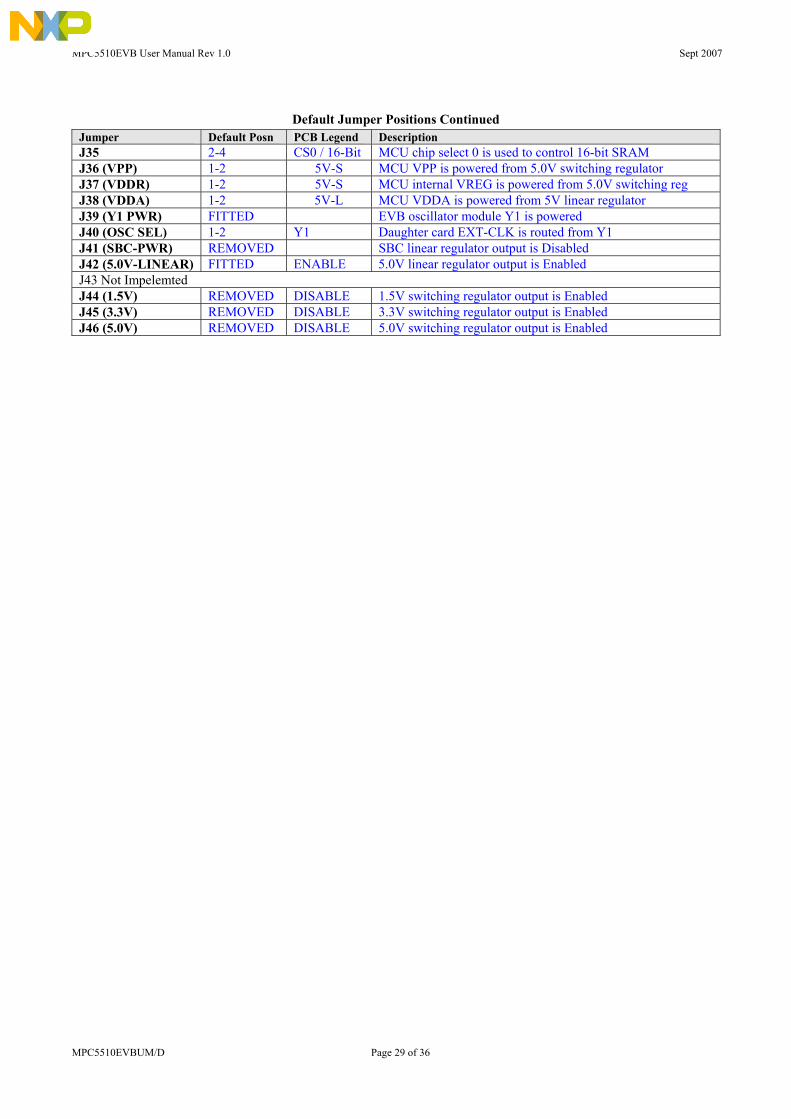
MPC5510EVB User Manual Rev 1.0 Sept 2007
MPC5510EVBUM/D Page 29 of 36
Default Jumper Positions Continued
Jumper Default Posn PCB Legend Description J35 2-4 CS0 / 16-Bit MCU chip select 0 is used to control 16-bit SRAM J36 (VPP) 1-2 5V-S MCU VPP is powered from 5.0V switching regulator J37 (VDDR) 1-2 5V-S MCU internal VREG is powered from 5.0V switching reg J38 (VDDA) 1-2 5V-L MCU VDDA is powered from 5V linear regulator J39 (Y1 PWR) FITTED EVB oscillator module Y1 is powered J40 (OSC SEL) 1-2 Y1 Daughter card EXT-CLK is routed from Y1 J41 (SBC-PWR) REMOVED SBC linear regulator output is Disabled J42 (5.0V-LINEAR) FITTED ENABLE 5.0V linear regulator output is Enabled J43 Not Impelemted J44 (1.5V) REMOVED DISABLE 1.5V switching regulator output is Enabled J45 (3.3V) REMOVED DISABLE 3.3V switching regulator output is Enabled J46 (5.0V) REMOVED DISABLE 5.0V switching regulator output is Enabled
MPC5510EVB User Manual Rev 1.0 Sept 2007
MPC5510EVBUM/D Page 30 of 36
The user connectors are located on the right hand side of the PCB 7. User Connector Descriptions
This section details the pinout of the EVB user connectors. The connectors are 0.1 inch pitch turned pin headers and are located to the right hand side of the EVB. Pins are grouped by port functionality and the PCB legend shows the respective port number adjacent to each pin. Shaded GREEN areas represent pins that are shared with the Nexus port Shaded BLUE areas represent a GPIO pin that is also used on the EVB for another purpose Note that not all of the port functionality is available on all of the derivatives. Please consult your particular MCU documentation for details on available ports.
7.1.1 Port A / ADC (Connector P16, RV1 and J8)
Table 7-1 Port A Connector Pinout (P16)
Function Availability Function Availability Pin GPIO 1st Alt 144 176 208 Pin GPIO 1st Alt 144 176 208 1 PA0 AN0 2 PA1 AN1 3 PA2 AN2 4 PA3 AN3 5 PA4 AN4 6 PA5 AN5 7 PA6 AN6 8 PA7 AN7 9 PA8 AN8 10 PA9 AN9 11 PA10 AN10 12 PA11 AN11 13 PA12 AN12 14 PA13 AN13 15 PA14 AN14 16 PA15 AN15 17 GND
18 GND To provide a quick means of supplying input to the ATD (Analogue To Digital converter), a 2KΩ variable resistor (RV1) will be connected between P5V and GND, with the output (centre tap) connected to PA0 / AN0 via jumper J8. By removing jumper J8, PA0 is disconnected from the variable resistor and can function as a normal I/O port. J8 and RV1 are located in the top right hand corner of the EVB
Table 7-2 RV1 Connection Jumper J8 Jumper Position PCB Legend Description
FITTED (D) Output from variable resistor RV1 is applied to MCU PA0 J8 (RV1) REMOVED
Output from RV1 is not connected to MCU (disabled)
Note - PA14 and PA15 can also be used for the EXTAL32 and XTAL32 32Khz reference clock. If these pins are used for this purpose, they will not be available for GPIO / ADC input. See section 4.2.3 for details.
7.1.2 Port B / ADC / SCI (P30)
Table 7-3 Port B Connector Pinout (P30)
Function Availability Function Availability Pin GPIO 1st Alt 144 176 208 Pin GPIO 1st Alt 144 176 208 1 PB0 AN28 2 PB1 AN29 3 PB2 AN30 4 PB3 AN31 5 PB4 AN32 6 PB5 AN33 7 PB6 AN34 8 PB7 AN35 9 PB8 AN36 10 PB9 AN37 11 PB10 AN38 12 PB11 AN39 13 PB12 TXD_G 14 PB13 RXD_G 15 PB14 TXD_H 16 PB15 RXD_H 17 GND
18 GND

MPC5510EVB User Manual Rev 1.0 Sept 2007
MPC5510EVBUM/D Page 31 of 36
7.1.3 Port C / ADC / SCI (P24)
Table 7-4 PortC Connector Pinout (P24)
Function Availability Function Availability Pin GPIO 1st Alt 144 176 208 Pin GPIO 1st Alt 144 176 208 1 PC0 eMIOS[0] 2 PC1 eMIOS[1] 3 PC2 eMIOS[2] 4 PC3 eMIOS[3] 5 PC4 eMIOS[4] 6 PC5 eMIOS[5] 7 PC6 eMIOS[6] 8 PC7 eMIOS[7] 9 PC8 eMIOS[8] 10 PC9 eMIOS[9] 11 PC10 eMIOS[10] 12 PC11 eMIOS[11] 13 PC12 eMIOS[12] 14 PC13 eMIOS[13] 15 PC14 eMIOS[14] 16 PC15 eMIOS[15] 17 GND
18 GND Notes:
- PC[0..11] is used to drive the LED dot matrix display if enabled. See section 3.10 for details. - PC[0..2] and PC[7..9] are also used for the flexray interface. See section 3.9 for details.
7.1.4 Port D / CAN / SCI / SPI (P15)
Table 7-5 PortD Connector Pinout (P15)
Function Availability Function Availability Pin GPIO 1st Alt 144 176 208 Pin GPIO 1st Alt 144 176 208 1 PD0 CNTX_A 2 PD1 CNRX_A 3 PD2 CNRX_B 4 PD3 CNTX_B 5 PD4 CNTX_C 6 PD5 CNRX_C 7 PD6 TXD_A 8 PD7 RXD_A 9 PD8 TXD_B 10 PD9 RXD_B 11 PD10 PCS_B[2] 12 PD11 PCS_B[1] 13 PD12 PCS_B[0] 14 PD13 SCK_B 15 PD14 SOUT_B 16 PD15 SIN_B 17 GND
18 GND Notes:
- PD2 is used for BOOTCFG data. See section 3.3.3 - PD0, PD1, PD4 and PD5 are used for the EVB CAN interface. See section 3.6 - PD6, PD7, PD8 and PD9 are used on the EVB SCI / LIN Physical Interfaces. See sections 3.7 and 3.8 - PD12, PD13, PD14, PD15 are used by the SBC SPI communication. See section 3.1.5 -
7.1.5 PortE / SPI / eMIOS / EIM (Connector P31)
Table 7-6 PortE Connector Pinout (P31)
Function Availability Function Availability Pin GPIO 1st Alt 144 176 208 Pin GPIO 1st Alt 144 176 208 1 PE0 PCS_A[2] 2 PE1 PCS_A[1] 3 PE2 PCS_A[0] 4 PE3 SCK_A 5 PE4 SOUT_A 6 PE5 SIN_A 7 PE6 CLKOUT 8 PE7 --- 9 PE8 eMIOS[24] 10 PE9 eMIOS[25] 11 PE10 eMIOS[26] 12 PE11 eMIOS[27] 13 PE12 eMIOS[28] 14 PE13 eMIOS[29] 15 PE14 eMIOS[30] 16 PE15 eMIOS[31] 17 GND
18 GND Note – Port PE6 has a 33ohm series resistor close to the MCU on the MCU daughter-card to provide some CLKOUT impedance matching. This can be disabled with a jumper if required. See the daughter-card user manual for details.

MPC5510EVB User Manual Rev 1.0 Sept 2007
MPC5510EVBUM/D Page 32 of 36
7.1.6 Port F / EIM (Connector P17)
Table 7-7 Port F Connector Pinout (P17)
Function Availability Function Availability Pin GPIO 1st Alt 144 176 208 Pin GPIO 1st Alt 144 176 208 1 PF0 RD_WR 2 PF1 TA 3 PF2 AD[8] 4 PF3 AD[9] 5 PF4 AD[10] 6 PF5 AD[11] 7 PF6 AD[12] 8 PF7 AD[13] 9 PF8 AD[14] 10 PF9 AD[15] 11 PF10 CS[1] 12 PF11 CS[0] 13 PF12 TS 14 PF13 OE 15 PF14 WE[0] 16 PF15 WE[1] 17 GND
18 GND Notes
- PF[0..15] are used to drive the EBI. See section 3.5 - PF[0..11] are used for the Nexus interface. When using Nexus, the EBI must be disabled and nothing connected
to these GPIO pins. See section 3.4
7.1.7 Port G / EIM (Connector P25)
Table 7-8 Port F Connector Pinout (P25)
Function Availability Function Availability Pin GPIO 1st Alt 144 176 208 Pin GPIO 1st Alt 144 176 208 1 PG0 AD[16] 2 PG1 AD17] 3 PG2 AD[18] 4 PG3 AD[19] 5 PG4 AD[20] 6 PG5 AD[21] 7 PG6 AD[22] 8 PG7 AD[23] 9 PG8 AD[24] 10 PG9 AD[25] 11 PG10 AD[26] 12 PG11 AD[27] 13 PG12 AD[28] 14 PG13 AD[29] 15 PG14 AD[30] 16 PG15 AD[31] 17 GND
18 GND Note – PG[0..15] are used to drive the EBI. See section 3.5
7.1.8 Port H / ADC / API / EIM (Connector P29)
Table 7-9 Port H Connector Pinout
Function Availability Function Availability Pin GPIO 1st Alt 144 176 208 Pin GPIO 1st Alt 144 176 208 1 PH0 AN[27] 2 PH1 AN[26] 3 PH2 AN[25] 4 PH3 AN[24] 5 PH4 AN[23] 6 PH5 AN[22] 7 PH6 AN[21] 8 PH7 AN[20] 9 PH8 AN[19] 10 PH9 AN[18] 11 PH10 AN[17] 12 PH11 AN[16] 13 PH12 PCS_D[5] 14 PH13 --- 15 PH14 WE[2] 16 PH15 WE[3] 17 GND
18 GND Note – PH[14..15] are used to drive the EBI (32-bit data port mode). See section 3.5

MPC5510EVB User Manual Rev 1.0 Sept 2007
MPC5510EVBUM/D Page 33 of 36
7.1.9 Port J / EIM / SPI (Connector P23)
Table 7-10 Port J Connector Pinout
Function Availability Function Availability Pin GPIO 1st Alt 144 176 208 Pin GPIO 1st Alt 144 176 208 1 PJ0 AD[0] 2 PJ1 AD[1] 3 PJ2 AD[2] 4 PJ3 AD[3] 5 PJ4 AD[4] 6 PJ5 AD[5] 7 PJ6 AD[6] 8 PJ7 AD[7] 9 PJ8 PCS_D[4] 10 PJ9 PCS_D[3] 11 PJ10 PCS_D[2] 12 PJ11 PCS_D[1] 13 PJ12 PCS_D[0] 14 PJ13 SCK_D 15 PJ14 SOUT_D 16 PJ15 SIN_D 17 GND
18 GND Note –PJ[0..7]are used to drive the EBI (32-bit data port mode). See section 3.5
7.1.10 Port K / EXTAL32 / XTAL32 (Connector P33)
Table 7-11 Port K Connector Pinout
Function Availability Function Availability Pin GPIO 1st Alt 100 144 208 Pin GPIO 1st Alt 100 144 208 1 PK0 EXTAL32 2 PK1 EXTAL32 17 GND
18 GND Note – The EXTAL32 and XTAL32 function is available on pins PA14 and PA15 for all packages that do not provide PortK.

MPC5510EVB User Manual Rev 1.0 Sept 2007
MPC5510EVBUM/D Page 34 of 36
The prototyping area is located
on the right hand side of the EVB, above the user connectors.
7.2 Prototyping Area and User LED’s / Switches There is a rectangular prototype area on the EVB, consisting of a 0.1inch pitch array of through-hole plated pads. Power from all three voltage regulators is readily accessible along with GND. This area is ideal for the addition of any custom circuitry. Adapters are available to convert SMD devices to 0.1inch pitch through-hole. Note the power supply lines to the prototype area are connected directly to the regulator outputs and not connected to the jumpered MCU supply. There are 4 active low user LED’s DS4, DS5, DS6 and DS7, These are driven by connecting a logic 0 signal to the corresponding pin on 0.1” header P10 (user LED’s). There are 4 active high pushbutton switches SW2, SW3, SW4 and SW5 which will drive 5V onto the respective pins on 0.1” connector P11 when pressed. The switch outputs are pulled to GND with a 10K resistor network.

MPC5510EVB User Manual Rev 1.0 Sept 2007
MPC5510EVBUM/D Page 35 of 36
8. Daughter Card Connectors (P9, P22)
The daughter card connectors are located roughly in the centre of the board. .
As mentioned previously, there are two 120-way expansion connectors fitted to the EVB, allowing connection of an MCU daughter card or another board providing functionality enhancement. The part numbers of possible connectors are detailed in Table 8-1 below.
Table 8-1 Expansion Connector Part Numbers
Connector Location Height Pitch TYCO / AMP Part Number EVB 8mm 0.8mm 179031-5
9mm 0.8mm 5-179009-5 Daughter Card 13mm 0.8mm 5-179010-5 The pinout of the expansion connectors is detailed below for reference.
Table 8-2 Daughter Card Connector 1
Pin Number
Signal Name (0dd)
Signal Name (Even)
Pin Number
Signal Name (0dd)
Signal Name (Even)
1 PB2 PB12 61 PH7 PH3 3 PK0 PA13 63 PH4 PJ8 5 PA8 3.3V-SR 65 PJ9 GND 7 VDDA VDDA 67 VDDE2 VDDE2 9 VDD VDD 69 PH0 PH1
11 3.3V-SR PB3 71 GND PH2 13 PB13 PK1 73 PG12 PG13 15 VDD VDD 75 PG14 PG15 17 PA12 GND 77 PF8 GND 19 PB4 PB0 79 PF12 PF15 21 PA15 PA11 81 VDDE2 VDDE2 23 GND PA9 83 GND PG9 25 PA6 PA7 85 PG10 PG11 27 PB5 PB1 87 PF7 PF11 29 PA14 GND 89 PF14 GND 31 PA10 PA3 91 PG0 PG3 33 PA4 PA5 93 VDDE2 VDDE2 35 GND MCU-RST 95 5.0V-SR PG8 37 -- PA0 97 PJ7 PF10 39 PA1 PA2 99 PF13 PH15 41 PH10 GND 101 PG2 5.0V-SR 43 PH11 PH12 103 PG5 PG7 45 PH13 PJ13 105 VDD VDD 47 GND PJ14 107 P12V PF6 49 PH9 PJ15 109 PF9 PH14 51 VDDE2 VDDE2 111 VDDR VDDR 53 PJ11 GND 113 PG1 P12V 55 PJ12 PH8 115 PG4 PG6 57 PJ10 PH5 117 VDD VDD 59 GND PH6 119 TGT-RST RST-OUT

MPC5510E
MPC5510E
VB User Manual Rev 1.0 Sept 2007
VBUM/D Page 36 of 36
Table 8-3 Daughter Card Connector 2
Pin Number
Signal Name (0dd)
Signal Name (Even)
Pin Number
Signal Name (0dd)
Signal Name (Even)
1 PB6 PB10 61 PE8 PE9 3 PB15 PC3 63 PD14 PE11 5 PC7 GND 65 PE10 GND 7 VDDE1 VDDE1 67 PE12 PD15 9 VDD VDD 69 VDDE1 VDDE1
11 GND PC10 71 GND PE0 13 PB7 PB11 73 PE13 PE1 15 PC0 PC4 75 PE2 PE14 17 PC8 GND 77 PE3 GND 19 VDD VDD 79 PE15 PE5 21 PC11 PC12 81 VDDE3 VDDE3 23 GND PB8 83 GND PJ2 25 PB14 PC1 85 PJ0 PF0 27 PC5 PC9 87 VDD33 VDD33 29 PC13 GND 89 PE4 GND 31 PC14 PB9 91 CLK-IN PJ6 33 VDDE1 VDDE1 93 PJ4 PJ1 35 GND PC2 95 GND PF1 37 PC6 PC15 97 VPP VPP 39 PD0 PD1 99 PE6 PF5 41 PD2 GND 101 PJ3 GND 43 VDDE1 VDDE1 103 PF2 TDI 45 PD3 PD4 105 VDD VDD 47 GND PD5 107 1.5V-SR TCLK 49 PD6 PD7 109 VDDSYN VDDSYN 51 PD9 PD8 111 PJ5 PF4 53 PD10 GND 113 VDDE3 1.5V-SR 55 VDDE1 VDDE1 115 VDDE3 PF3 57 PD11 PD12 117 JCOMP TDO 59 PE7 PD13 119 TMS VDD
Notes:
- Power connections shown with red shading are from the outputs of the respective MCU power jumpers. The power connections shown in orange shading (1.5V-SR, 3.3V-SR, 5.0V-SR and P12V) are direct outputs from the regulators / main power input and are not jumpered. These are designed to drive any non-MCU daughter card circuitry.
- The TGT-RESET signal provides a mechanism of driving the MCU reset line from a non open-drain source. This can be used by a target system to control the system reset. RST-OUT is a driven reset signal which should be connected to Reset-in of any custom devices on the daughter card. The MCU-Reset line provides a direct connection to the bidirectional MCU Reset pin. Extreme caution should be exercised if this pin is used.
- All of the MCU signals with the exception of VRH, VRL, EXTAL, XTAL, and REFBYPC, are routed to the connectors.

MPC
5516
EVB
Use
r Man
ual R
ev 1
.0
S
ept 2
007
App
endi
x Th
e EV
B a
nd d
augh
terc
ard
BO
M (B
ill o
f Mat
eria
ls) a
nd S
chem
atic
s are
det
aile
d in
the
App
endi
x as
show
n be
low
.
App
endi
x ID
D
escr
iptio
n A
ppen
dix
A -
EV
B S
chem
atic
s (R
ev E
0)
App
endi
x B
-
EVB
Bill
Of M
ater
ials
A
ppen
dix
C -
14
4QFP
Dau
ghte
rcar
d Sc
hem
atic
s (R
ev B
1)
App
endi
x D
-
144Q
FP D
augh
terc
ard
Bill
Of M
ater
ials
A
ppen
dix
E -
176Q
FP D
augh
terc
ard
Sche
mat
ics (
Rev
C0)
A
ppen
dix
F -
176Q
FP D
augh
terc
ard
Bill
Of M
ater
ials
A
ppen
dix
G -
20
8BG
A D
augh
terc
ard
Sche
mat
ics (
Rev
B1)
A
ppen
dix
H -
20
8BG
A D
augh
terc
ard
Bill
Of M
ater
ials
M
PC55
16EV
BU
M/D
Pa
ge B
-1

MPC
5516
EVB
Use
r Man
ual R
ev 1
.0
S
ept 2
007
App
endi
x A
-
EV
B S
chem
atic
s
A. R
ober
tson
10 D
ec 2
006
Des
igne
r0.
1
Revis
ion
Info
rmat
ion
Cha
nged
P3
and
P4 fr
om 2
mm
to 2
.54m
m
Prov
ision
al (P
re B
ack
Ann
otat
ion)
B0A
. Rob
ertso
n
07 A
ug 2
007
D1
A. R
ober
tson
Add
itiona
l pow
er o
n D
C. P
roto
Rele
ase
- PC
B Re
vA0.
203
Jan
2007
FCL
Prod
n Re
lease
- PC
B Re
vB03
Jul 2
007
11 Ju
l 200
7Fi
xed
conn
ectiv
ity o
n Po
wer
Jack
(P28
)C
0
Dat
eR
evC
omm
ents
Cha
nged
Pow
er S
uppl
y C
aps (
C13
, C14
, C15
& C
20)
A. R
ober
tson
A. R
ober
tson
A. R
ober
tson
10 S
ept 2
007
D2
D0
31 Ju
l 200
7
Post
FCL
Tidy
Up.
Cor
rect
ion
to J1
3 / J
15A
. Rob
ertso
n
Dra
win
g Ti
tle:
Size
Doc
umen
t N
umbe
rR
ev
Dat
e:Sh
eet
of
Page
Titl
e:
Des
igne
r:
Dra
wn b
y:
App
rov
ed:
Tran
spor
tatio
n &
Sta
ndar
d Pr
oduc
ts G
roup
MC
D A
pplic
atio
ns E
ast K
ilbrid
eC
olv
illes
Roa
d, K
elvi
n In
dust
rial E
stat
e, E
ast
Kilb
ride
G75
0TG
SCH
-231
30
PD
F:
SPF
-231
30E0
MP
C551
0 Ev
alua
tion
Boar
d
B
Wed
nesd
ay,
Sept
embe
r 12
, 20
07
Fron
t Pag
e C
onte
nts
and
Note
s
A.
Rob
erts
on
A.
Rob
erts
on
A.
Rob
erts
on
114
Thes
e sc
hem
atic
s ar
e pr
ovid
ed fo
r ref
eren
ce p
urpo
ses
only
. As
such
, Fre
esca
le do
es n
ot m
ake
any
war
rant
y, im
plied
or
othe
rwise
, as
to th
e su
itabi
lity
of c
ircui
t des
ign
or c
ompo
nent
selec
tion
(type
or v
alue)
use
d in
thes
e sc
hem
atic
s fo
r har
dwar
ede
sign
usin
g th
e Fr
eesc
ale M
PC55
10 fa
mily
of
Mic
ropr
oces
sors
. Cus
tom
ers
usin
g an
y pa
rt of
thes
e sc
hem
atic
sas
a b
asis
for h
ardw
are
desig
n, d
o so
at t
heir
own
risk
and
Free
scale
doe
s no
t ass
ume
any
liabi
lity
for s
uch
a ha
rdw
are
desig
n.Specific PCB LAYOUT notes are detailed in ITALICS
User notes are given throughtout the schematics.
- All test points are denoted TPx
- Test Point Vias are denoted TPVx
Not
e:
A. R
ober
tson
12 S
ept 2
007
Relea
sed
to P
rodu
ctio
n - P
CB
RevE
E0
POWER SUPPLY 2 (SBC AND VOLTAGE ROUTING)
SRAM
TERMINATION RESISTORS
SHEE
T 10
- Variable resistors are denoted RVx
SHEE
T 9
SHEE
T 8
- Resistor networks are donated RNx. All resistor networks are SMD 1206 style package.
- All decoupling caps less than 0.1uF are COG unless otherwise stated
SHEE
T 2
SHEE
T 7
USER IO CONNECTORS (PORT HEADERS)
POWER SUPPLY 1 (INPUT, LINEAR AND SWITCHERS)
Tabl
e O
f Con
tent
s:
SCI AND LIN TRANSCEIVERS
CAN TRANSCEIVERS
SHEE
T 13
USER (PROTOTYPE) AREA AND I/O PEIPHERALS
DAUGHTERCARD CONNECTORS
FLEXRAY TRANSCEIVERS
Notes:
- All components and board processes are to be ROHS compliant
SHEE
T 14M
PC55
10 E
valu
atio
n B
oard
JTAG AND NEXUS CONNECTORS
RESET GENERATION, CONTROL AND BOOTCFG
SHEE
T 5
SHEE
T 4
EVB CLOCK OSCILLATOR AND SMA CONNECTORS
- All jumpers are denoted Jx. Jumpers are 2mm pitch
SHEE
T 3
- All connectors are denoted Px. All connectors and headers are 2.54mm pitch unless otherwise stated
SHEE
T 11
SHEE
T 6
SHEE
T 12
- All decoupling caps greater than 0.1uF are X7R unless otherwise stated
- Jumper default positions are shown in the schematics. For 3 way jumpers, default is always posn 1-2
- All Switches are denoted SWx
MPC
5516
EVB
UM
/D
Page
B-2

MPC
5516
EVB
Use
r Man
ual R
ev 1
.0
S
ept 2
007
PT11
1
PT3
1
C80
0.1
UF
+C
1410
0uF
L5
100
UH
L347U
F
TP13
1
PT20
1
PT12
1
TP14
1
C83
0.1
UF
GN
DG
ND
P12
V_R
GN
D
P12V
GN
D
3.3V
_SR
GN
D
5.0V
_SR
P12
V
GN
D
GN
D
1.5V
_SR
GN
D
P12V
5.0V
_LR
GN
D
5.0V
_SR
GN
D
1.5V
_SR
3.3V
_SR
D8
B130LB-13
21
J42
12
D6
B130LB-13
21
D7
B130LB-13
21
Main Pow
er-I
n
J46
1 2
J45
1 2
J44
1 2
Vout
= 1
.21(1
+ R2
/R1)
GND Test Points
F1
Fuse
Hol
der
12
POWE
R SUPP
LY 1 (
Inpu
t and
Non-SB
C)
U22
LM26
76S-
5.0
INPU
T2
SW
_OU
T1
C_B
OO
ST3
GND4
TAB 8
FEE
DB
ACK
6
ON
/OFF
7
NC
5
Swit
chin
g R
egul
ator
s
3.3V
Sw
itchi
ng R
egul
ator
1.5V
Sw
itchi
ng R
egul
ator
Nexu
s Co
nnecto
rPowe
r Mo
nitor
Protoype Area Reference Points
5V S
witc
hing
Reg
ulat
or
U19
LM29
37-5
.0
VIN
1V
O3
GND 2
GND4
VS
witc
hed
2 Leve
rCo
nnec
tor
2.1mm
Barr
elCo
nnec
tor
Pow
er s
uppl
y in
put
and
filte
r
POW
ER S
WIT
CH
VFu
sed
U21
LM26
76S-
3.3
INPU
T2
SW
_OU
T1
C_B
OO
ST3
GND4
TAB 8
FEE
DB
ACK
6
ON
/OFF
7
NC
5
Test
and
ref
eren
ce p
oint
s
Title
Size
Doc
umen
t N
umbe
rR
ev
Dat
e:S
heet
of
Dra
win
g SC
H-2
3130
(MP
C55
10EV
B)
E0
MP
C55
10 E
valu
atio
n B
oard
B
214
Tues
day
, Se
ptem
ber
11,
2007
Free
scal
e M
CD
App
licat
ions
- E
ast K
ilbrid
e
5V L
inea
rReg
ulat
or
P28
1 2 3
D3
B130LB-13
21
(R2 =
2 Ress
itor
s in
serie
s)
U20
LM26
76S-
ADJ
INPU
T2
SW
_OU
T1
C_B
OO
ST3
GND4
TAB 8
FEE
DB
ACK
6
ON
/OFF
7
NC
5PT
151
C79 0.1
UF
PT4
1
+C
12 68U
F
C17
3.3U
F
+C
1310
0uF
12V
-IN
PT6
1
L647U
F
PT18
1
PT9
1
C84
1000
PF
R48 270 OHM
TP1 1
+C
1610
00U
F
TP15
1
L4
68U
H
TP4 1
PT17
1
TP8 1
+C
1510
0uF
PT13
1
Q3
BSH
103
1
23
R42
560
OH
M
PT19
1
TP5 1
TP12
1
R41
68 O
HM
R44
1.2K
TP3 1
R43
220
OH
M
C19
4.7u
F
PT16
1
R45
100
OH
M
PT1
01
DS
12
LED
GR
EEN2
1
TP10 1
TP2 1
PT1
1
C18
3.3U
F
TP9 1
PT5
1
DS
10
LED
GR
EE
N21
R46
1.80
K
R47 560 OHM
PT14
1
SW
6G
-107
-051
31
34
2
5
PT8
1
TP7 1
C82
0.1
UF
P32
A1
B2
PT7
1
DS
11
LED
GR
EE
N
21
TP6 1
TP11 1
DS
13
LED
GR
EEN2
1
PT2
1
C81
0.1
UF
+C
2010
0uF
MPC
5516
EVB
UM
/D
Page
B-3

MPC
5516
EVB
Use
r Man
ual R
ev 1
.0
S
ept 2
007
SBC
-SAF
E
J41
12
PD13
J27
12
PD15
- MASTER
SERIAL I
N (SLAVE O
UT)
PD14
- MASTER
SERIAL O
UT (SLAVE
IN)
J38
1
2
3
J25
12
SBC
-MIS
O
J37
1
2
3
EB
CQ2
BC
P52-
16
1
3 24
J34
1
2
3
PD14
SBC
-VA
UX
(SCK-B)
(SOUT-B)
(SIN-B)
MC
U-R
STx
5,6,
11
J33
1
2
3
SBC
-RM
CU
-RST
x
P26
13 24
J30
1
2
3
J29
1
2
3
PD15
SBC
-DB
G
+
C9
10U
F
C78
0.1
UF
GN
D
SBC
-IN
TV
DD
E1
VBau
x
SBC
-VC
AN
SBC
-LIN
2
SBC
-LIN
2RX
SBC
-LIN
2TX
VE VB
PD
[0..
15]
R35
60.4
OH
M
GN
D
C71
2200
PF
(AN1)
(MCU A
DC)
TPV
24
SBC
-VA
UX
SBC
-VD
D
SBC
-VD
D
GN
D
POWE
R SU
PPLY
2 (SB
C an
d Ro
utin
g Ju
mper
s)
R34
60.4
OH
M
MCU DS
PI-B
J21
12
R53
0 O
HM
(PCS-B0)
SBC
-CAN
H
C74
0.1
UF
C76
0.1
UF
VCau
x
C77
0.1
UF
External V
aux
transistor
External
VDD
transistor
CAN
Transceive
rand Regula
tor
LIN
Transceive
r
MCU SPI CO
MMS
U18 MC
3390
5S
5V-C
AN
6
SAFE
5
INT
23
VCau
x12
Vsense20
IO-0
15
Vaux
13
RST
22
VBa
ux11
IO-1
21
MU
X-O
UT
14
LIN
-T4
RXD
-L19
TXD
-L18
DBG
16
CSB
24
SCLK
25
MO
SI26
MIS
O27
SPL
IT10
CA
NH
7C
AN
L8
VD
D28
TXD
29R
XD30
VBA
SE32
VEM
31
VSUP1
IO-3
3
VSUP12
TAB33
GND_CAN9
LIN
17
5.0V)
(5.0V)
(5.0V)
(3.3V /
SBC
-VC
AN
P12
V
GN
D
VIN
aux
C75
0.1
UF
GN
D
PA1
R40
1.0K
P19
1 2 3
(3.3v Switch
er)
(3.3v Switch
er)
(5/ SBC)
(5/ SBC)
v Switch
v Switch
VD
DE1
11
5.0V
_LR
(I/O Seg
(5v Switch
er)
ment 1)
PD
[0..1
5]5,
8,9,
11,1
2
VD
DA
(ADC Sup
ply)
VD
DA
11SB
C-V
DD
VD
DE2
nt 2)
(I/O Segme
VD
D33
11
VD
DE2
11
SBC
-IO
1
VD
DE3
VDD
33
(SBC 5v M
(SBC 5v Ma
in)
ain)
VD
DE3
11nt 3)
(I/O Segme
VD
DSY
N11
1.5V
_SR
V3.
3-5.
0
VDD
SY
N
(5v Swit
cher)
VD
D15
e supply
(MCU cor
when
NOT usin
g VReg)
VD
D15
11
VPP
V3.
3-5.
0
(Fla
sh Progr
amming)
VPP
11
V3.
3-5.
0
(1.5v Switch
er)
VDDR jumper MUST be in posn 2-3 when VDD33, VDDSYN or VDD15 jumpers are fitted
(SBC 5v CA
N)
(5/ SBC)
(5v Switch
er)
/5V)
(5v Li
near)
(3.3v Switch
er)
v Switch
(SBC 3.3
VD
DR
11
3.3V
_SR5.
0V_S
R
VD
DR
(On Chip
Regulato
r)
(3.3v Switch
er)
PD12
(3.3v Switch
er)
SBC
-CS
SBC
-M
+
C10
10U
F
J43
12
34
56
78
910
1112
C8
4.7u
F
+
C11
10U
F
J36
1
2
3
SBC
-IO
0
SBC
-SC
LK
D4
GF
1A2
1
Title
Size
Doc
umen
t Num
ber
Rev
Dat
e:Sh
eet
of
Dra
win
g S
CH
-231
30
(MPC
5510
EVB)
E0
MP
C55
10 E
valu
atio
n B
oard
B
314
Mon
day
, Se
ptem
ber
10,
2007
Free
scal
e M
CD
App
licat
ions
- E
ast K
ilbrid
e
SBC
GN
D
GN
D
GN
D
R37
1.0K
C72
0.1
UF
SBC
-CN
TX
SBC
-SP
LIT
SBC
-CN
RX
R52
10K
PA[
0..1
5]P
A[0.
.15]
11,1
2,13
SBC
-CAN
L
P18
1 32 4 5
EB
C
Q1 BCP52-16
1
3 24
SBC
-MO
SI
MPC
5516
EVB
UM
/D
Page
B-4

MPC
5516
EVB
Use
r Man
ual R
ev 1
.0
S
ept 2
007
C73
0.1
UF
R38
100
OH
M
From
dau
ghte
r ca
rdP
E6
J39
12
GN
D
Note - External 3.3V
regulator MUST be
enabled when using
oscillator module
SMA style
Connector
P21
1
2435
OS
C-M
OD
EVB
-EXT
AL
EVB
-EXT
AL11
Car
d)(To
Daug
hter
CLK
OUT
Vdd
gnd
Y1
8MH
z4 2
31
FB2
12
GN
D
(PE6
CLK
OUT)
PE[
0..1
5]6,
7,11
,12
PE
[0..
15]
P27
1
2435
CLOCK
CIRCUITRY
EXT
AL-
SM
A
GN
D
SMA style
Connector
FB1
12
Note - Internal
Pull-Up on Pin 1
3.3V
_SR
FB3
12
(CLK
OUT)
J40
1
2
3
Title
Size
Doc
umen
t N
umbe
rR
ev
Dat
e:S
heet
of
Dra
wing
SC
H-2
3130
(MP
C55
10E
VB)
E0
MP
C55
10 E
valu
atio
n B
oard
B
414
Mon
day
, S
epte
mbe
r 10,
200
7
Free
scal
e M
CD
App
licat
ions
- E
ast K
ilbrid
e
MPC
5516
EVB
UM
/D
Page
B-5

MPC
5516
EVB
Use
r Man
ual R
ev 1
.0
S
ept 2
007
Buffered
RESET-OUT
Title
Siz
eD
ocum
ent
Num
ber
Rev
Dat
e:S
heet
of
Dra
win
g S
CH
-231
30
(M
PC
5510
EV
B)
E0
MP
C55
10 E
valu
atio
n B
oard
B
514
Mon
day
, S
epte
mbe
r 10,
200
7
Free
scal
e M
CD
App
licat
ions
- E
ast K
ilbrid
e
GN
D
R16
10K
RS
T-O
UTx
MCU RESET LED
R22
1.2K
AC08 / AC125
Decoupling
Caps
R23
470
OH
M
GN
D
5.0V
_SR
RS
TCF
G
JTA
G-R
STx
TGT-
RS
TxLV
I-R
STx
VC
C
GN
DU
8A
SN
74LV
125
23
141
7
5VL-
RS
Tx
(Fro
m Ex
pans
ion
Conn
/ Us
er C
onne
ctor
s)TG
T-R
STx
11,1
2
U8B
SN
74LV
125
56
4
J19
1
2
3
U8C
SN74
LV12
5
98
10
U8D
SN
74LV
125
1211
13
MC
U-R
STx
3,6,
11
TGT-
RS
Tx
5.0V
_SR
RN
6
10K
1 2 3 45678
J20
12
34
VC
C
GN
DU9A
MC
74A
CT0
8DG
1 23
14 7
U9B
MC
74A
CT0
8DG
4 56
UNUSED
PAR
TSG
ND
U9C
MC
74A
CT0
8DG
9 108
U9D
MC
74A
CT0
8DG
12 1311
BO
OTC
FG
-R
GN
D
SW
1K
S11
R23
CQ
D 1
3
42
GN
D
5.0V
_SR
GN
D
PD
[0..
15]
RS
T-O
UTx
BO
OTC
FG
-R6
5.0V
_LR
(All
ows
Nexu
s to
dri
ve B
OOTC
FG at
rese
t)
PD
3
PD
2
JTA
G-R
STx
6
LVI Circuit
IF P
FI <
1.2
5V,
PFO
Goes
LOW
4.65
V Th
resh
old
LVI
J17
12
RESET
CONTRO
L
5.0V
_SR
5.0V
_SR
(Rev
0)
Tri-State Buffered RESET signal to MCU (Reset-IN)
USR RESET LED
R18
560
OH
M
DS
1
YE
LLO
W L
ED
21
5.0V
_SR
5.0V
_SR
JTA
G-R
STx
MC
U-R
STx
PD
[0..
15]
3,8,
9,11
,12
5.0V
_SR
(Fro
m JT
AG /
NEX
US)
Seri
al Boo
t Mo
de
Inte
rnal F
lash
R17
560
OH
M
Boot Config
DS
2
LED
RE
D
12
5.0V
_SR
GN
D
R13
10K
R15
Do
Not
Fit
LVI-
RS
Tx
RS
T-O
UTx
6,7,
11,1
2
BO
OTC
FG
GN
D
C45
0.1
UF
U11
MA
X705
CS
A+
MR
1
VC
C2
GN
D3
PF
I4
PF
O5
WD
I6
RE
SE
T7
WD
O8
C44
0.1
UF
(Rev
A+)
GN
D
C52
0.1
UF
Rese
t-In
Disa
ble
(App
rox
1.4V
Out
)
GN
D
5.0V
_SR
GN
D
R14
0 O
HM
5VL-
RS
Tx
MPC
5516
EVB
UM
/D
Page
B-6

MPC
5516
EVB
Use
r Man
ual R
ev 1
.0
S
ept 2
007
MPC
5516
EVB
UM
/D
Page
B-7
RS
T-O
UTx
RS
T-O
UTx
EVT
I
PF5
(Ven
dor I/
O 4)
(Ven
dor I/
O 1)
UBAT
T
VALT
REF
UBAT
T(T
ool
I/O
0)
PF6
TDO
R50
0 O
HM
Do
Not
Fit
R51
0 O
HM
Title
Size
Doc
umen
t Num
ber
Rev
Dat
e:S
heet
of
Dra
win
g SC
H-2
3130
(M
PC55
10E
VB)
E0
MP
C55
10 E
valu
atio
n B
oard
B
614
Mon
day
, Sep
tem
ber
10,
2007
Free
scal
e M
CD
App
licat
ions
- E
ast K
ilbrid
e
EVT
I
GN
D
PF7
J31B
1
2
3
V-D
BU
G
(RDY)
(CLK
OUT)
PF8
5.0V
_SR
Nexus target sense voltage select
TCLK
11,1
4
PF9
(MSE
O[1]
)
(MDO
[2])
(MCK
0)(EVT
O)
(MDO
[3])
(MDO
[4])
(MDO
[0])
VREF
(MDO
[1])
(MDO
[5])
(Ven
d IO
-3)
(MDO
[6])
PF1
0(MDO
[7])
(RDY
)
RW
7
V-D
BU
G
(EVT
I)
(MSE
O[0]
)
PF1
1
JTAG
-RS
Tx
TCLK
PF2PE
6
(RW
for
RAM)
MC
U-R
STx
MC
U-R
STx
3,5,
11
PF[
0..1
5]7,
11,1
2,14
TCLK
R36
10K
NEXUS Connector
VEN
DO
R-IO
-2
5.0V
_SR
G1..
G5 =
MIC
TOR
Cent
re G
roun
d Pi
ns
P14
11
22
33
44
55
66
77
88
99
1010
1111
1212
1313
1414
1515
1616
1717
1818
1919
2020
2121
2222
2323
2424
2525
2626
2727
2828
2929
3030
3131
3232
3333
3434
3535
3636
3737
3838
G3
41
G4
42
G5
43G
139
G2
40
SET-
IN B
uffe
r)
(PE6
CLK
OUT)
ONCE
AND
NEXUS C
ONNECTORS
TMS
(To
RE
PE[
0..1
5]P
E[0.
.15]
4,7,
11,1
2
(Dir
ect
to M
CU-R
eset
pin
)
TMS
11,1
4
(Too
l I/O
2)(TIO
3)
(Too
l I/O
1)
P13
HD
R 2
X7
12
34 6
5 78
910
1112
1314
JCO
MP
11,1
4
(Ven
dor I/
O 0)
Must
be
open
-dra
in o
utpu
t wi
th a
bili
ty t
odr
ive su
ffic
ient
cur
rent
to
over
come
10K
pull
up /
pul
ldow
n)
V-D
BUG
V-D
BU
G
TDI
TDI
EVT
I
TPV1
5
C66
47P
F
Do
Not
Fit
Place CAPS as close to
connector pins as
possible but do NOT fit
caps at board assembly.
BOO
TCF
G-R
5TD
O
TCLK
TMS
(EVT
I / RW
)
PF0
P12V
_R
JCO
MP
TDI
TDI
11,1
4
TPV1
6(A
llows
Nexu
s PR
OBE
to d
rive
BOO
TCFG
at
rese
t)
JCO
MP
JCO
MP
JTA
G-J
RS
Tx
R49
10K
3.3V
_SR
TPV1
7
NEXUS Conenctor (MICTOR)
TDO
11,1
4
RS
T-O
UTx
5,7,
11,1
2TP
V18
JTAG
-RS
Tx5
Jump
er a
llow
s JT
AG R
ESET
to
be r
oute
d v
iabu
ffer
s or
to be
dir
ectl
y co
nnec
ted
to t
he M
CURE
SETx
bi-
direct
iona
l pi
n (f
or d
ebug
har
dwar
eth
at c
an m
onitor
the
sta
te o
f th
e ta
rget
res
et).
TPV1
9
C61
47P
F
Do
Not
Fit
TPV
20
ONCE Connector
(TRS
T)
TPV2
1
GN
D
TPV2
2TP
V23
PF[
0..1
5]
PF3
Allows
Nex
us t
ool
to m
onit
or M
CU r
eset
sta
te
GN
D
TDO
RW
PF1
GN
D
J31
1
2
3
(N/C)
(VSS)
(VSS)
(VSS)
(VSS)
JTA
G-J
RST
x
J24
12
BOO
TCFG
-R
TMS
PF4

MPC
5516
EVB
Use
r Man
ual R
ev 1
.0
S
ept 2
007
RW
GAL
-TM
S
AD
DR
17
AD
DR
31
AD
DR
21
AD
DR
18
AD
DR
16
AD
DR
20A
DD
R19
AD
DR
30
AD
DR
22
AD
DR
28
AD
DR
26A
DD
R27
AD
DR
29
AD
DR
24A
DD
R25
AD
DR
23
RW
6
(BE3)
CS-
32
AD
DR
15A
DD
R16
AD
DR
17A
DD
R18
AD
DR
19
AD
DR
25A
DD
R26
AD
DR
27A
DD
R28
AD
DR
14
AD
DR
29
AD
DR
20A
DD
R21
AD
DR
22A
DD
R23
AD
DR
24
GAL
-TD
O
CS
-32
RST
-OU
Tx
GA
L-ST
GN
D
(GAL
Latch and Status LED's)
TSTA
(Address Latches when
ALE is LOW)
Local Decoupling for all 3
SRAM parts
(PE6 CLK
OUT)
GN
D
PH
[0..1
5]11
,12,
14
C67
0.1
UF
C68
0.1
UF
C69
470P
F
C70
1000
PF
GN
D
PF[
0..1
5]
GAL
-TD
I
GN
D
TP-I
/O6
(BE1)
RW
PF1
4
ALE
-CLR
SRAM
-5V
GN
D
Title
Size
Doc
umen
t Num
ber
Rev
Dat
e:Sh
eet
of
Dra
wing
SC
H-2
3130
(M
PC55
10EV
B)E0
MP
C55
10 E
valu
atio
n B
oard
B
714
Mon
day
, Sep
tem
ber
10, 2
007
Free
scal
e M
CD
App
licat
ions
- E
ast K
ilbrid
e
AD
DR
16A
DD
R17
AD
DR
18A
DD
R19
AD
DR
25A
DD
R26
AD
DR
27A
DD
R28
AD
DR
15
AD
DR
20A
DD
R21
AD
DR
22A
DD
R23
AD
DR
24
PF10
AD
DR
30A
DD
R29
(CS1
)
(CS0
)
C56
0.1
UF
PH
14
C50
470P
F
C55
0.1
UF
C51
1000
PF
PF1
5
GA
L-VC
C
TP-I
/O7
CS
-16
(BE0)
ALE
CLKO
UT
PH
14(Alter
native
Footpr
int)
SRAM-5V
BE[2]
BE[1]
D[16..23]
D[8..15]
BE[3]
BE[1]
D[24..31]
BE[0]
BE[1]
BE[0]
WE/BE 32-BIT PORT
Data Acces
sBE[0]
WE/B
E 16-BIT PORT
D[0..7]
Note the exc
eption for 16-bit port usi
ng DATA[16..31]
CS
-32
GAL
-TD
O
ADD
R[1
4..3
0]
P12
12
34 6
5 78
910
ADD
R15
PF11
PF8
PF1
PF12
PF14
PF13
PF10
PF9
RW
PF155.
0V_S
R
PE6
GN
D
GN
D
(AD25)
(AD26)
(AD27)
(AD28)
(AD29)
(AD31)
(AD24)
PG13
PG11
PG8
PG9
PG15
PG12
PG10
(AD23)
PG6
PG7
(AD20)
(AD21)
(AD30)
(AD22)
CS
-32
(AD17)
(AD18)
(AD19)
PG4
PG2
PG1
PG14
PG3
PG5
(AD16)
PG0
J35
24
6 13
5
X X 0
1
GAL
-TD
I
RW
PF11
C47
0.1
UF
PF1
3
C49
470P
F
C46
0.1
UF
C48
1000
PF
(CS1
)
RST
-OU
Tx
In 16-bit Da
ta bus mode (DBM set to 1
in MCR), the
EIM can be c
onfigured to use DATA[0..1
5] or
DATA[16..31]
by writing to D16_31 bit
in MCR. The
EVB is confi
gured for Data[16..31]
0 0 1
X
(Alt
ernative
Foot
print)
ALE
-CLR
TP-I/
O6
ALE
-SET
AD
DR
14A
DD
R15
TP-I/
O7
GA
L-AL
E
TP-I/
O5
PG
13P
G12
PG
11P
G10
PG
9
(D27)
(D28)
(D29)
(D30)
PG
14
(D22)
(D23)
(D24)
(D25)
(D26)
(D17)
(D18)
(D19)
(D20)
(D21)
(D31)
(D16)
PG
2P
G1
PG
0
PG
15
PG
7P
G6
PG
5P
G4
PG
3
PG
8
(CLK
OUT)
(AD14)
(TA)
LSB
PF8
PF1
PF12
(CS1)
(CS0)
(TS)
RW
PF11
****
3.3V
_SR
PF9
(WE0)
(OE)
**PF
10
(WE1)
(AD15)
RST
-OU
Tx5,
6,11
,12
PF14
PF15
PF13
0 1 1
0
PG
[0..1
5]11
,12
PG[0
..15
]
GN
D
(CS0
)
MSB
SR
AM-5
V
1 0 1
1
GN
D
CS
-16
16-BIT Memory System:
ADD
R14
PF1
5
PE6
(OE)
PF1
3
1 1 1
1
GN
D
C62
0.1
UF GN
D
C6
470P
F
C7
0.1
UF
C65
1000
PF
PH
15
RN
9
10K
1 2 3 45678
IDT IDT74FCT162373AT
TI CY74FCT16373 / CY74
FCT162373T
Compatible Buffers:
TPV
9
TPV
12TP
V11
TPV
10
AD
DR
18A
DD
R19
AD
DR
27A
DD
R28
AD
DR
14A
DD
R15
AD
DR
16A
DD
R17
AD
DR
22A
DD
R23
AD
DR
24A
DD
R25
AD
DR
26
GAL
-LT
AD
DR
29
AD
DR
20A
DD
R21
J22
12
GN
D
PG
11P
G10
PG
9
PG
14P
G13
PG
12(D27)
(D28)
(D29)
(D30)
(D22)
(D23)
(D24)
(D25)
(D26)
(D17)
(D18)
(D19)
(D20)
(D21)
(D11)
(D12)
(D13)
(D14)
(D15)
(D16)
(D6)
(D7)
(D8)
(D9)
(D10)
U12
IS61
C64
16AL
-12T
LI
A0
44
A1
43
A2
42
A3
27
A4
26
A5
25
A6
24
A7
21
A8
20
A9
19
A10
18
A11
5
A12
4
A13
3
A14
2
A15
1
I/O0
7
I/O1
8
I/O2
9
I/O3
10
I/O4
13
I/O5
14
I/O6
15
I/O7
16
I/O8
29
I/O9
30
I/O
1031
I/O
1132
I/O
1235
I/O
1336
I/O
1437
I/O
1538
CE
6
WE
17
OE
41
UB
40
LB39
VDD
_11
11
VDD
_33
33
GN
D_1
212
GN
D_3
434
NC
_23
23
NC
_28
28N
C_2
222
(D1)
(D2)
(D3)
(D4)
(D5)
(D0)
PF6
PF5
PF4
PF3
PJ2
PJ1
PJ0
PF9
PF8
PF7
PJ7
PJ6
PJ5
PJ4
PJ3
PF2 MSB
LSB
PG
15(D31)
PG
0P
G1
PG
2P
G3
PG
5P
G4
C59
0.1
UF
C60
0.1
UF
C63
470P
F
PG
6
C64
1000
PF
32-BIT Memory System (2*16-bit)
PF1
3
PG
8P
G7
GN
D
PE[0
..15]
J32
1 2
(BE3)
(BE2)
(BE1)
(BE0)
(OE)
PF1
4 (OE)
U16 I/C
LK2
TCK
1
TDI
15TM
S8
TDO
22G
ND
14
I/O1
17
I/O2
18
I/O3
19
I/O4
20
I/O5
21
I/O6
23
I/O7
24
I/O8
25
I/O9
26
I/O10
27
VCC
28I1
3
I24
I35
I46
I57
I69
I710
I811
I912
I10
13
I11
16
U14
IS61
C64
16AL
-12T
LI
A0
44
A1
43
A2
42
A3
27
A4
26
A5
25
A6
24
A7
21
A8
20
A9
19
A10
18
A11
5
A12
4
A13
3
A14
2
A15
1
I/O0
7
I/O1
8
I/O2
9
I/O3
10
I/O4
13
I/O5
14
I/O6
15
I/O7
16
I/O8
29
I/O9
30
I/O
1031
I/O
1132
I/O
1235
I/O
1336
I/O
1437
I/O
1538
CE
6
WE
17
OE
41
UB
40
LB39
VDD
_11
11
VDD
_33
33
GN
D_1
212
GN
D_3
434
NC
_23
23
NC
_28
28N
C_2
222
TPV
13TP
V14
GAL
-TC
KG
AL-S
T
PF[
0..1
5]
R33
10K
GAL
-ALE
U15
ispG
AL22
V10
AV-2
3LN
N
I11
14I1
010
I99
I88
I77
I66
I53
I42
I31
I232
I131
I/CLK
30IO
Q8
17
IOQ
1015
IOQ
916
IOQ
718
IOQ
619
IOQ
522
IOQ
324
IOQ
423
IOQ
225
IOQ
126
TCK
29
TMS
4
TDI
13
TDO
21
VCC
O5
GN
DO
20
GN
D11
VCC
28
VCC
O27
GN
DO
12
TAB
33
GAL
-TC
KGAL
-VC
C
GN
D
GAL
Power
Control
GAL
-VC
C
U17
IS61
C64
16AL
-12T
LI
A0
44
A1
43
A2
42
A3
27
A4
26
A5
25
A6
24
A7
21
A8
20
A9
19
A10
18
A11
5
A12
4
A13
3
A14
2
A15
1
I/O0
7
I/O1
8
I/O2
9
I/O3
10
I/O4
13
I/O5
14
I/O6
15
I/O7
16
I/O8
29
I/O9
30
I/O
1031
I/O
1132
I/O
1235
I/O
1336
I/O
1437
I/O
1538
CE
6
WE
17
OE
41
UB
40
LB39
VDD
_11
11
VDD
_33
33
GN
D_1
212
GN
D_3
434
NC
_23
23
NC
_28
28N
C_2
222
R32
10K
SRAM
-5V
PF15
RW
PF13
PF14
Pullups on
SRAM CS lines. Ensures
that when
SRAM is disabled, and CS
jumpers re
moved from selet jumper,
no pullup
signal on PF10 / 11
GAL
-ALE
(OE)
PF[
0..1
5]6,
11,1
2,14
PE[0
..15
]4,
6,11
,12
(BE0)
(BE2)
R30
270
OH
MD
S9
21
R31
270
OH
M
DS
82
1
PJ[0
..15
]11
,12
CS-
16
GA
L-LT
GN
D
ALE
-SET
PG
[0..1
5]
PJ[
0..1
5]
(BE1)
EXTERNA
L SR
AM
PH
[0..1
5]
U10
74F
CT1
6237
3ATP
ACT
1OE
1
1O1
2
1O2
3
GN
D4
1O3
5
1O4
6
VCC
7
1O5
8
1O6
9
GN
D10
1O7
11
1O8
12
2O1
13
2O2
14
GN
D15
2O3
16
2O4
17
VCC
18
2O5
19
2O6
20
GN
D21
2O7
22
2O8
23
2OE
242L
E25
2D8
262D
727
GN
D28
2D6
292D
530
VC
C31
2D4
322D
333
GN
D34
2D2
352D
136
1D8
371D
738
GN
D39
1D6
401D
541
VC
C42
1D4
431D
344
GN
D45
1D2
461D
147
1LE
48
De-Latch address when
TA is low
(and CLKOUT rising edg
e)
Latch address when TS
is low (and
CLKOUT rising edge)
Connected to bus
entry at left hand
side of sheet)
GAL
-TM
S
PH
15
TP-I
/O5
MPC
5516
EVB
UM
/D
Page
B-8

MPC
5516
EVB
Use
r Man
ual R
ev 1
.0
S
ept 2
007
(CNC
-TX)
(CNC
-RX)
C28
1000
PF
CAN PH
YSICAL I
NTERFACE
GN
D
CA
NC
-RS
P3
1 2 3
P41 2 3
CAN
A-TX
PD
0P
D1
CAN
A-R
S
5.0V
_SR
Title
Size
Doc
umen
t Num
ber
Rev
Dat
e:S
heet
of
Dra
wing
SC
H-2
3130
(MP
C55
10E
VB)
E0
MP
C55
10 E
valu
atio
n B
oard
B
814
Mon
day
, Sep
tem
ber 1
0, 2
007
Free
scal
e M
CD
App
licat
ions
- E
ast K
ilbrid
e
GN
DG
ND
R6
0 O
HM
PD
[0..1
5]3,
5,9,
11,1
2
CA
NA-
CAN
H
J31
23
4
CA
NA-
CAN
L
J4 HD
R 2
X2
12
34
GN
D
CAN
A-R
X
GN
D
J71
2
U1
PC
A82
C25
0TD
TXD
1
RS
8
RXD
4
VR
EF
5
GN
D2
VC
C3
CA
NH
7
CA
NL
6
U2
PC
A82
C25
0TD
TXD
1
RS
8
RXD
4
VR
EF
5
GN
D2
VC
C3
CA
NH
7
CA
NL
6
Rs = 0 Ohms for High Speed Operation. Replace
with non zero resistor to enable slope
control.
(CNA
-RX)
CANC
CAN
C-C
ANL
CAN
C-C
ANL
CAN
C-C
ANH
CAN
C-C
ANH
(CNA
-TX)
GN
D
PD
4
CANA
GN
D
CA
NC
-TX
PD
5
C36
1000
PF
PD[0
..15]
Note - CANB Rx on initial MPC5516
Si is shared with BootCFG so it was
decided not to use this as one of
the default CAN modules
C35
0.1
UF
CA
NC
-RX
CAN
-5V
C27
0.1
UF
GN
D
R5
0 O
HM
MPC
5516
EVB
UM
/D
Page
B-9

MPC
5516
EVB
Use
r Man
ual R
ev 1
.0
S
ept 2
007
GN
D
PD
8
(RXD-B
)
(TXD-B
)
PD
9
LIN
A-TX
D1 GF
1A
21
D2
GF
1A
21
LIN
B-R
X
PD
7
U4
MC
Z333
99
RXD
1
EN
2
WAK
E3
TXD
4G
ND
5LI
N6
VS
UP
7IN
H8
U3
MC
Z333
99
RXD
1
EN
2
WAK
E3
TXD
4G
ND
5LI
N6
VS
UP
7IN
H8
RS
232-
5
P12
V
Note -
The S
BC pro
vides
anothe
r 2 LI
NPh
ysic
al int
erface
s whic
h can
be con
nected
by use
r to u
ser co
nnecto
rs wit
h jump
erwi
res
U7
MA
X232
ACSE
+
C1+
1
C1-
3
C2-
5C
2+4
V+
2
V-6
T1O
UT
14
T2O
UT
7T1
IN11
T2IN
10
R1I
N13
R2I
N8
R1O
UT
12
R2O
UT
9
GND15
VCC16
J11
2
Title
Size
Doc
umen
t N
umbe
rR
ev
Dat
e:S
heet
of
Dra
win
g S
CH
-231
30
(MP
C55
10EV
B)
E0
MP
C55
10 E
valu
atio
n B
oard
B
914
Tues
day
, S
epte
mbe
r 11
, 20
07
Free
scal
e M
CD
App
licat
ions
- E
ast K
ilbrid
e
J91
2
J51
2
J61
2
5.0V
_SR
LIN
B-TX
GN
D
LIN
A-R
X
P5 D
B9
594837261
M2
M1
LIN
B-R
XG
ND
SCIA
-RX
SCIA
-RX
SCIA
-TX
SCIA
-TX
SCI
and
LIN
PHYSIC
AL I
NTER
FACE
S
R9
10K
RS
232B
-RX
PD
6
SCI / RS232
RS
232A
-TX
RS
232A
-RX
P6 D
B9
594837261
M2
M1
GN
D
GN
D
Note - If a MAX232A device is
used, the 5 polorised 1uF caps
can be reduced to 0.1uF
R7
1.0K
RS
232-
4
LIN
A-L
IN
GN
D
RS
232-
VC
C
GN
D
Master Mode Pullup Enable
LINA
PD[0
..15
]3,
5,8,
11,1
2
LIN
A-V
SU
P
C29
1000
PF
C31
0.1
UF
RS2
32 T
ER
MIN
AL
PO
RT
9-W
AY
D-T
YP
E (F
emal
e)
C5
1000
PF
GN
D
C41
1.0U
F
(TXD-A
)
C37
1.0U
F
C42
1.0U
F
C43
1.0U
F
(RXD-A
)
C40
1.0U
F
RS
232-
1
SCIB
-RX
SCIB
-RX
LIN
A-R
X
SCIB
-TX
SCIB
-TX
PD
[0..
15]
LIN
A-TX
GN
D
Enable
d as l
ong
as EN
> 3.5V
GN
D
RS
232-
3
RS
232B
-TX
5.0V
_SR
P7
1 32 4
P8
1 32 4
J10
24
6 13
5
J11
24
6 13
5
J21
2
P12
V
R10
10K
5.0V
_SR
GN
D
GN
D
R8
1.0K
GN
D
LIN
B-L
IN
Master Mode Pullup Enable
C30
1000
PF
LINB
LIN
B-V
SU
P
C32
0.1
UF
GN
D
LIN
B-TX
Enab
led as
long
as E
N > 3.
5V
MPC
5516
EVB
UM
/D
Page
B-1
0

MPC
5516
EVB
Use
r Man
ual R
ev 1
.0
S
ept 2
007
R3
47 O
HM
FRA
-WA
KE
FR
A-IN
H1
Port
C[0.
.15] i
s in t
he V
DDE1 p
ower
domai
n whic
h ca
nbe s
elec
ted be
tween
3.3v
and 5
V. T
he pow
er con
trol
jump
er a
llows
select
ion
of the
app
ropria
te I/O
volt
age
to use
on th
e Fl
exray
PHI
+C3 10UF
PC1
FR-1
2V
C39 0.1 UF
FRB
-JR
XD
L1
DLW
43S
H
21 4
3
FR-5
V
L2
DLW
43SH
21 4
3
PC0
GN
D
FRA
-BG
EGN
DPC
2
P12
V
Flexray A
FRA
-JR
XD
Flexray B
FR-V
IO
GN
D
FRA-
JTXD
RN
4
10K
1 2 3 45678
P1
1 2
3.3V
_SR
RN
5
10K
1 2 3 45678
FR
-VIO
Crim
ped
lead -
279-9
522
Rece
ptac
le hou
sing -
279
-9156
FRA-
JTXE
N
FLEX
RAY PH
YSICAL I
NTERFA
CE
Title
Size
Doc
umen
t N
umbe
rR
ev
Dat
e:S
heet
of
Dra
win
g SC
H-2
3130
(M
PC55
10E
VB)
E0
MP
C55
10 E
valu
atio
n B
oard
B
1014
Mon
day,
Sep
tem
ber 1
0, 2
007
Free
scal
e M
CD
App
licat
ions
- E
ast K
ilbrid
e
J13
12
34
56
78
GN
D
R12
47K
TPV
1
J12
12
34 6
5
FR
A-D
ATA
-B
GN
D
TPV
2
FR
A-B
M
J18
1
2
3
U6
TJA1
080T
S/N
TRXD
011
TRXD
110
TXD
5
TXE
N6
BGE
8
STBN
9
EN3
WAK
E15
INH
21
INH
12
BP
18
BM
17
RXD
7
ERR
N13
RXE
N12
VIO4
VCC19
VBUF20
VBAT14 GND16
TPV
3
U5
TJA1
080T
S/N
TRXD
011
TRXD
110
TXD
5
TXE
N6
BGE
8
STBN
9
EN3
WAK
E15
INH
21
INH
12
BP
18
BM
17
RXD
7
ERR
N13
RXE
N12
VIO4
VCC19
VBUF20
VBAT14 GND16
Normal
Sleep
1STBN
EN
TPV
4
1 110
Rec Only
Go to Sl
eep
0 00
MODE
TPV7
TPV5
TPV6
TPV
8
J14
HD
R 2
X3
12
34 6
5
FRA
-STB
N
FR
-VIO
FR
A-B
P
R4
47 O
HM
R1
47 O
HM
FR
B-IN
H2
+C4 10UF
PC8
C38 0.1 UF
GN
D
PC9
FRB
-BG
E
PC7
GN
D
P2
1 2
FR
B-JT
XD
Crim
ped
lead -
279-9
522
Rece
ptac
le hou
sing -
279
-9156
FR
B-JT
XEN
GN
D
R11
47K
FR
B-B
MFR
B-S
TBN
FR
B-D
ATA-
B
R2
47 O
HM
FR
B-B
P
C33 0.1 UF
FRB
-EN
C22
4700
PF
FR
B-IN
H1
GN
D
FRB
-RXE
N
C23
10 P
F
FR
-VIO
FR
B-D
ATA-
A
FR
B-E
RR
NC
2110
PF
+C2 10UF
C34 0.1 UF
FRA
-EN
FR
-5V
C25
4700
PF
FRB
-WA
KE
FR
A-IN
H2
PC[0
..15]
FR
A-D
ATA
-A
FR
-5V
FR
A-R
XEN
GN
D
C26
10 P
F
FR-V
IO
J16
HD
R 2
X3
12
34 6
5
J15
12
34
56
78
PC
[0..
15]
11,1
2,13
FR
A-E
RR
N
FR
-12V
5.0V
_SR
FR
-12V
+C1 10UF
C24
10 P
F
VIO Se
lectio
n Jump
er
Note - Flexray is 2nd
Alternate function of
PortC Pins
MPC
5516
EVB
UM
/D
Page
B-1
1

MPC
5516
EVB
Use
r Man
ual R
ev 1
.0
S
ept 2
007
TMS
PH
9
PG
4
PG
9
PF
13
PJ8
5.0V
_SR
VDD1
5
PB
6
PJ1
2
PD
4
VD
D15
PG
13P
E1
F
PG
10
PC
[0..
15]
PA
[0..
15]
PH
[0..1
5]
PB[
0..1
5]
VDDE
1
VDDE
VDDE
VDDE
1
11
PD
[0..
15]
PK
[0..
1]P
K[0
..1]
PF
5
PB
5
PE
4
MC
U-R
STx
PA
7
3.3V
_SR
VD
DE
23
PJ[
0..1
5]
VD
DR
PB
13
PB
4
PB
7
PC
[0..
15]
10,1
2,13
PK
0
PC
11
VD
D15
PD
13
TDO
P12
VVD
DE3
VDDE
3
PJ1
0
Jump
ered
()
PB
2
RS
T-O
UTx
5,6,
7,12
Jump
ered
()
PH
14P
12V
1.5V
_SR
PG
2
TGT-
RS
Tx5,
12
PE
6
PA
10
VDDE
2
VP
P
J
PJ6
5.0V
_SR
PA
14
VDDE
2
H
3.3V
_SR
VD
D33
PC
5
PD
2
umpe
red)
B
(J
PE
14
PC
10
PH
1
PE
11
VDD
E2
TMS
PH
8P
D11
PE
8
J
PJ2
PG
[0..
15]
7,12
TMS
6,14
P9 1
12
2
33
44
55
66
77
88
99
1010
1111
1212
1313
1414
1515
1616
1717
1818
1919
2020
2121
2222
2323
2424
2525
2626
2727
2828
2929
3030
3131
3232
3333
3434
3535
3636
3737
3838
3939
4040
4141
4242
4343
4444
4545
4646
4747
4848
4949
5050
5151
5252
5353
5454
5555
5656
5757
5858
5959
6060
6161
6262
6363
6464
6565
6666
6767
6868
6969
7070
7171
7272
7373
7474
7575
7676
7777
7878
7979
8080
8181
8282
8383
8484
8585
8686
8787
8888
8989
9090
9191
9292
9393
9494
9595
9696
9797
9898
9999
100
100
101
101
102
102
103
103
104
104
105
105
106
106
107
107
108
108
109
109
110
110
111
111
112
112
113
113
114
114
115
115
116
116
117
117
118
118
119
119
120
120
PH
[0..
15]
7,12
,14
TDO
6,14
PB
10
VDD
SY
N
G
PF
10
PG
12P
G15
PG
11
PB
1
MC
U-R
STx
MC
U-R
STx
CONNECTORS MUST BE PLACED IN
ACCORDANCE WITH PCB SPECIFICATION
PF
7
PB
[0..
15]
12
PH
[0..
15]
VDD
E3
3umpe
red)
(JVD
DE
3
PE
13
VDD
E1
3
VD
DR
3
B
PD
5
VD
DA
F
PF
2
VD
DR
JCO
MP
VDD
E1
PH
5
PC
2
1.5V
_SR
J
PJ1
3
PC
13
Conenctor 1
PB
14
PH
2
PB
[0..
15]
PC
0
PH
7
VD
D15
3
P12
V
PE
5
VD
DS
YN
TDI
6,14
DAUGHT
ERCARD
CON
NECT
ORS
PG
5
P22
11
22
33
44
55
66
77
88
99
1010
1111
1212
1313
1414
1515
1616
1717
1818
1919
2020
2121
2222
2323
2424
2525
2626
2727
2828
2929
3030
3131
3232
3333
3434
3535
3636
3737
3838
3939
4040
4141
4242
4343
4444
4545
4646
4747
4848
4949
5050
5151
5252
5353
5454
5555
5656
5757
5858
5959
6060
6161
6262
6363
6464
6565
6666
6767
6868
6969
7070
7171
7272
7373
7474
7575
7676
7777
7878
7979
8080
8181
8282
8383
8484
8585
8686
8787
8888
8989
9090
9191
9292
9393
9494
9595
9696
9797
9898
9999
100
100
101
101
102
102
103
103
104
104
105
105
106
106
107
107
108
108
109
109
110
110
111
111
112
112
113
113
114
114
115
115
116
116
117
117
118
118
119
119
120
120
PJ0
VDD1
5
(NC)
VDD
33VD
D33
3
VDD
15VD
D15
PD
7
PC
12
VD
DA
3
PH
6
VDD
E1
AMP Connector Part number 179031-5 (8mm high, 0.8mm pitch 120way)
PG
7
Suitable Mating connector - AMP 5-179009-5 (9mm high) or 5-179010-5 (13mm high)
PB
11
VDDE
2VD
DE2
VDDE
2
PD
3
F
PH
12
PF
[0..
15]
6,7,
12,1
4
PJ1
(Jum
pered)
PD
15
PE
0
PF
[0..
15]
PF
11
PC
1
PC
14
VDDE
2
PC
15
PC
8
PF
9
F
PD
[0..
15]
3,5,
8,9,
12
PF
15
VD
D15
3.3V
_SR
PF
[0..
15]
PG
14
VDDE
2
PF
3
DC
PB
0
Title
Siz
eD
ocum
ent
Num
ber
Rev
Dat
e:S
heet
of
Dra
win
g SC
H-2
3130
(M
PC55
10E
VB
)E
0
MP
C55
10 E
valu
atio
n B
oard
B
1114
Mon
day
, S
epte
mbe
r 10
, 20
07
Free
scal
e M
CD
App
licat
ions
- E
ast K
ilbrid
e
PF
8
PF
14
PH
3
PA
[0..
15]
PJ3
PA
15
PD
8
PB
3
Jump
ered
()
VDD
15VD
D15
PE
2
PB
12
JCO
MP
EV
B-E
XTAL
PD
14P
H4
H
PH
10
PA4
TCLK
6,14
TCLK
TCLK
PA
0
E
PA
3
VDD1
VDD1
5 5
PD
6
PJ4
PA
8
PJ5
PJ[
0..1
5]7,
12
PB
8
PJ[
0..1
5]P
J[0.
.15]
PB
[0..
15]
PG
[0..
15]
PC
4
VD
D15
PE
10
1.5V
_SR
PA
1
PC
[0..
15]
PG
0
VD
DA
VD
DA
PA
[0..
15]
3,12
,13
PA
13
PC
6
VDDE
3
JCO
MP
6,14
PA
11
TDO
PF
6
PC
9
TGT-
RS
Tx
PG
3
VPP
3
PJ9
RS
T-O
UTx
PA
2
KK
AA
BB
PE
3
PK
1
PB
[0..
15]
PF
0
PF
1V
PP
PG
1
C
PB
15
VD
DE2
J
PJ1
1
PE
[0..
15]
PG
[0..1
5]
PF
[0..
15]
PE
7
VDDE
1
PJ1
4
er(J
ump
ed)
VDD1
5
PD
9
EV
B-E
XTA
L
PH
11
GND
E
PE
9
D
PD
1
MC
U-R
STx
3,5,
6
VDDE
1
GND
GND
GND
GND
GND
GND
GND
GND
GND
GND
GND
GND
GND
5.0V
_SR
VDD
SY
N3
PJ7
VDD1
5
VDD1
5
VDDE
1
EVB
-EXT
AL
4
PD
0
PG
8
VDD15
TDI
TDI
VDD15
PA
12
PJ1
5
VDDE
1
(Jumpe
red)
VD
DE
3
PH
13
PE
15
PA
6
PE
[0..
15]
4,6,
7,12
PF
12
PC
7
PK
[0..
1]12
umpe
red)
(J
G
PB
9
PC
3
GN
D
PD
10
Conenctor 2
PA
5
PA
9
PE[0
..15
]
PE
12
RS
T-O
UTx
PH
0
PF
4
GN
D
PD
12
15 15
VDD1
5
VDD
VDD
PH
15
GND
GND
GND
GND
GND
GND
GND
GND
GND
GND
GND
GND
GND
GND
GND GN
DG
ND
PG
6
MPC
5516
EVB
UM
/D
Page
B-1
2

MPC
5516
EVB
Use
r Man
ual R
ev 1
.0
S
ept 2
007
GN
D
(AD18)
(AD1
7)(AD16)
(AD2
5)(AD24)
(AD2
3)(AD22)
(AD2
1)(AD20)
(AD1
9)
PG7
PG13
PG1
PG0
PG9
PG3
PG14
PG15
PG4
PG12
PG10
PG6
GN
D
P25
12
34 6
5 78
910
1112
1314
1516
1718
PG2
PG11
PG5
GN
D
PortG / EIM (AD)P
G[0
..15]
7,11
PG
[0..1
5]
(eMIOS
0)PortC / eMIOS
PC[0
..15]
10,1
1,13
PC7
PC8
PC13
PC[0
..15]
PC1
PC0
PC14
PC15
P24
12
34 6
5 78
910
1112
1314
1516
1718
PC3
GN
D
PC10
PC6
PC9
PC11
PC4
PC12
PC5
PC2
GN
D
RST
-OU
Tx
PA0
(CNRX-A)
(RXD-B)
(CNTX-
A)(C
NTX-B)
(AN03)
(AN0
2)(A
N01)
(AN0
0)
(AN11)
(AN1
0)(A
N09)
(AN0
8)(A
N07)
(AN0
6)(A
N05)
(AN0
4)
(TXD-A
)
(AN15)
(AN1
4)(A
N13)
(AN1
2)
(RXD-A)
(CNRX-
B)
(TXD-B
)
(AD3
1)(AD30)
(AD2
9)(AD28)
(AD2
7)(AD26)
(AN2
8)
PE1
PE7
PortE / SPI /
eMIOS / EIM
PE[0
..15]
4,6,
7,11
PE8
PE13
PE[0
..15]
PE0
PE3
PE14
PE15
PE9
P31
12
34 6
5 78
910
1112
1314
1516
1718
PE10
PE6
GN
D
PE4
PE12
PE5
PE2
PE11
GN
D
PG8
PA2
USER
CONNE
CTOR
S
(AN31)
(AN29)
(TXD
_H)
(TXD
_G)
(AN3
8)(AN3
6)(AN3
4)(AN3
2)(AN3
0)
NOTE
: Al
l Conn
ectors
are 0
.1" th
roug
h-hole
heade
rs
PF1
PF7
PF8
PF13
PF0
PF14
PF15
PF10
PF6
PF9
PF3
P17
12
34 6
5 78
910
1112
1314
1516
1718
GN
D
PF4
PF12
PF5
PF2
PF11
GN
D
(AN17)
(AN1
8)(AN19)
(AN2
0)(AN21)
(AN2
2)(AN23)
(AN2
4)(AN25)
(AN2
6)(AN27)
(WE3
)(WE2)
(---
)(PCS-D5)
(AN1
6)
RST
-OU
Tx5,
6,7,
11
PortF / EIM
PA4
(PCS_B
0)(PCS_B
2)
(CNTX-
C)
(RXD_G)
(RXD_H)
(AN39)
(AN37)
(AN35)
(AN33)
TGT-
RS
Tx
PJ13
PJ1
PJ7
PJ0
PJ3
PJ14
PJ15
PJ12
PJ10
PJ6
PJ9
GN
D
PJ2
PJ11
PJ4
P23
12
34 6
5 78
910
1112
1314
1516
1718
PJ5
PJ[
0..1
5]7,
11
GN
D
PA[0
..15]
3,11
,13
PJ[
0..1
5]
PA[0
..15]
PortJ / EIM / SPI
PJ8
PB[0
..15]
11
PA6
PK1
PK0
GN
D
PH7
PH0
PH13
PH1
PH15
PK[
0..1
]11
GN
D
PK[
0..1
]
PH6
PH9
PH3
PH14
GN
D
PH4
PH12
PH10
PortK / Reset
PH2
PH11
P29
12
34 6
5 78
910
1112
1314
1516
1718
PH5
PH
[0..1
5]7,
11,1
4
GN
D
PortH / ADC /
SPI / EIM
PH
[0..1
5]
(PCS_B1)
PH8
(AD3
)(AD2)
(AD1
)(AD0)
(XTA
L32
(EXTAL32
)
(SIN
-D)
(SOUT-D)
(SCK
-D)
(PCS-D0)
(PCS
-D1
(PCD-D2)
(PCS
-D3
(PCS-D4)
(AD7
)(AD6)
(AD5
)(AD4)
)))PD
7
PortD / CAN /
SPI / SCI
PD[0
..15]
3,5,
8,9,
11PD
[0..1
5]
PD1
PA14
PA12
PA10
PA8
PD0
PD8
PD13
PD14
PD15
PD3
P15
12
34 6
5 78
910
1112
1314
1516
1718
PD9
GN
D
PD12
PD10
PD6
PD2
PD11
PD4
PD5
GN
D
P33
12
34 6
5
(CNRX-C)
(TO MCU)
(FROM MC
U)
PF[
0..1
5]
(R/W)
PA7
PA5
PA3
PA1
(AD10)
(AD8)
(WE1
)(OE)
(CS0
)(AD1
5)(AD1
3)(AD1
1)(AD9
)(TA)
(WE0)
(TS)
(CS1)
(AD14)
(AD12)
(eMIOS1)
(eMIOS15)
(eMIOS
14)
(eMIOS13)
(eMIOS
12)
(eMIOS11)
(eMIOS
10)
(eMIOS9)
(eMIOS
8)(e
MIOS7)
(eMIOS
6)(e
MIOS5)
(eMIOS
4)(e
MIOS3)
(eMIOS
2)
PortA / ADC
PortB / ADC / SPI
(SIN-B)
(SOUT-
B)(S
CK-B)
PB7
PB1
PB13
PB8
PB0
PB14
PB15
PF[
0..1
5]6,
7,11
,14
P30
12
34 6
5 78
910
1112
1314
1516
1718
PB3
GN
D
PB10
PB6
PB9
PB12
PB4
PB11
PB2PB
[0..1
5]
PB5
GN
D
Note - T
he LED M
atrix
is als
oco
nnecte
d to PC[
0..11]
PA15
PA13
PA11
PA9
Title
Size
Doc
umen
t Num
ber
Rev
Dat
e:Sh
eet
of
Dra
wing
SC
H-2
3130
(M
PC55
10EV
B)E0
MP
C55
10 E
valu
atio
n B
oard
B
1214
Mon
day,
Sep
tem
ber 1
0, 2
007
Free
scal
e M
CD
App
licat
ions
- E
ast K
ilbrid
e
TGT-
RST
x5,
11
(eMIOS31)
(eMIOS
30)
(eMIOS29)
(eMIOS
28)
(eMIOS27)
(eMIOS
26)
(eMIOS25)
(eMIOS
24)
(---)
(CLKOU
T)(S
IN-A)
(SOUT-
A)(S
CK-A)
(PCS-A
0)(P
CS-A1)
(PCS-a
2)
P16
12
34 6
5 78
910
1112
1314
1516
1718
GN
D
MPC
5516
EVB
UM
/D
Page
B-1
3
MPC
5516
EVB
Use
r Man
ual R
ev 1
.0
S
ept 2
007
LED
-C5
LED
-R6
PC5
LED
-RC
2
PC4
PC3
LED
Dot
Mat
rix
Dis
play
3.3V
_SR
LED
-RC
3
PC2
GN
D
PC1
R21
10K
LED
-RC
4
(UNUSE
D)(U
NUSE
D)
(UNUSE
D)(U
NUSE
D)
Local
Deco
upli
ngG
ND
GN
D
PC0
U13
SN
74LV
C16
244A
DG
GR
1Y1
2
1Y2
3
1Y3
5
1Y4
6
2Y1
8
2Y2
9
2Y3
11
2Y4
12
3Y1
13
3Y2
14
3Y3
16
3Y4
17
4Y1
19
4Y2
20
4Y3
22
4Y4
23
1A4
431A
344
1A2
461A
147
2A4
372A
338
2A2
402A
141
3A4
323A
333
3A2
353A
136
4A4
264A
327
4A2
294A
130
1OE
1
4OE
243O
E25
2OE
48
VCC
7
VCC
18
VCC
31
VCC
42
GN
D4
GN
D10
GN
D15
GN
D21
GN
D28
GN
D34
GN
D39
GN
D45
LED
-RC
5
PC10
LED
-OE-
HIG
H
3.3V
_SR
LED
-OE-
LOW
LED
-R1
R20
180
OH
M
2.2v
for
ward
volta
ge s
o R=18
0 Oh
ms
so r
un l
ed's
at ap
prox
6mA (
30mA
sink
onColu
mns)
Buff
ers
can
sink /
sou
rce ap
prox
max 5
0mA
C53
0.1
UF
LED
-R2
PC9
PC[0
..15]
10,1
1,12
PC
[0..1
5]
PC8
LED
-R3 R25
180
OH
M
GN
D
R24
180
OH
M
PC7
LED
-R7
PC11
PC6
R29
180
OH
M
R28
180
OH
M
LED
-RC
1
(eMIOS
11)
(eMIOS
6)(e
MIOS
7)(e
MIOS
8)(e
MIOS
9)
(eMIOS
10)
(eMIOS
0)(e
MIOS
1)(e
MIOS
2)(e
MIOS
3)
(eMIOS
4)
(eMIOS
5)
R19
10K
C57
470P
F
C54
1000
PF
C58 0.1
UF
RN
8
470O
HM
1 2 3 45678
RN
7
10K
1 2 3 45678
LED
-R4
P10
1 32 4
P11
1 32 4
DS
3LE
D 5
x7
R1
12
R2
11
R3
2
R4
9
R5
4
R6
5
R7
6
C1 1
C23
C3 10
C4 7
C5 8
LED
-C1
LED
-C2
US
R-S
W2
US
R-S
W3
Use
r Sw
itch
es
5.0V
_SR
DS5
21
DS6
21
DS4
21
DS7
21
SW
21
2
SW
41
2
SW
31
2
SW
51
2
GN
D
User
Per
iphe
rals Inc
Pro
toty
ping
US
R-S
W4
Use
r LE
D's
LED's ar
e SM
D (120
6) Y
ellow
US
R-S
W1
LED
-R5
OMRON
B3WN
-6002
Push
butt
on Swi
tch
5.0V
_SR
LED
-C3
J81
2
LED
-C4
J23
12
34 (A
N0)
GN
DPA
0
RV
12K
13
2
PA[
0..1
5]
AN
0 Po
tent
iom
eter
Title
Size
Doc
umen
t N
umbe
rR
ev
Dat
e:S
heet
of
Dra
wing
SC
H-2
3130
(M
PC55
10EV
B)E0
MP
C55
10 E
valu
atio
n B
oard
B
1314
Tues
day,
Sep
tem
ber 1
1, 2
007
Free
scal
e M
CD
App
licat
ions
- E
ast K
ilbrid
e
PA[
0..1
5]3,
11,1
2
5.0V
_LR
(Not
e - Th
is i
s run
from
lin
ear 5.
0v r
egulat
or t
o prov
ide
a st
able i
nput
volta
ge)
MPC
5516
EVB
UM
/D
Page
B-1
4

MPC
5516
EVB
Use
r Man
ual R
ev 1
.0
S
ept 2
007
MPC
5516
EVB
UM
/D
Page
B-1
5
5.0V
_SR
(BWE3)
(BWE2)
(BWE1)
(BWE0)
PF[0
..15]
6,7,
11,1
2
TDO
6,11
TDO
Title
Size
Doc
umen
t Num
ber
Rev
Dat
e:S
heet
of
Dra
win
g SC
H-2
3130
(M
PC55
10E
VB)
E0
MP
C55
10 E
valu
atio
n B
oard
B
1414
Wed
nesd
ay, S
epte
mbe
r 12,
200
7
Free
scal
e M
CD
App
licat
ions
- E
ast K
ilbrid
e
GN
D
PF13
PF12
J28
1
2
3
PH14
PH15
TCLK
J26
1 2
(TS)
(TA)
FM
4F
ID-0
4010
0 M
il M
ask
FM
3FI
D-0
4010
0 M
il M
ask
FM
2F
ID-0
4010
0 M
il M
ask
FM
1FI
D-0
4010
0 M
il M
ask
FM
8FI
D-0
4010
0 M
il M
ask
FM
5FI
D-0
4010
0 M
il M
ask
(OE)
For Single Chip mode
operation, need to isolate
pullup resistors from pins
that are mux'd with single
chip functions
RN
1
10K
1 2 3 45678
TDI
6,11
TMS
6,11
TCLK
6,11
RN
2
10K
1 2 3 45678
RN
3
10K
1 2 3 45678
GN
D
JTAG PORT
(JCO
MP / T
RST)
FM
7F
ID-0
4010
0 M
il M
ask
FM
6F
ID-0
4010
0 M
il M
ask
PF1
PH[0
..15
]
R27
10K
SRAM runs from 5V
so EIM pullups are
5V rather than
level of VDDE
JCO
MP
JCO
MP
6,11
All RESET Pullup Resistors are shown on Reset Circuitry page
TMS
TDI
PF[0
..15]
PF15
TERM
INATIO
N RE
SIST
ORS
V-D
BU
G
PF14
PH[0
..15
]7,
11,1
2
MPC
5516
EVB
Use
r Man
ual R
ev 1
.0
S
ept 2
007
App
endi
x B
-
EV
B B
ill O
f Mat
eria
ls
Q
ty
R
efde
sVa
lue
Man
ufac
ture
rPa
rt N
umbe
r4
C1,
C2,
C3,
C4
10U
F P
AN
AS
ON
IC
EE
E1C
S10
0SR
12
C
5,C
28,C
29,C
30,C
36,C
48,C
51,C
54,C
64,C
65,C
70,C
84
1000
PF
VE
NK
EL
CO
MP
AN
YC
0805
CO
G50
0-10
2JN
E
6
C
6,C
49,C
50,C
57,C
63,C
6947
0PF
KE
ME
TC
0805
C47
1J5G
AC
35
C
7,C
27,C
31,C
32,C
33,C
34,C
35,C
38,C
39,C
44,C
45,C
46,C
47,C
52,C
53,C
55,C
56,C
58,C
59,C
60,C
62,C
67,C
68,
C72
,C73
,C74
,C75
,C76
,C77
,C78
,C79
,C80
,C81
,C82
,C83
0.1
UF
KE
ME
T C
0805
C10
4K5R
AC
2
C
8,C
19
4.7u
F M
UR
ATA
GR
M32
ER
71H
475K
3
C9,
C10
,C11
10U
F V
ISH
AY
INTE
RTE
CH
NO
LOG
Y29
3D10
6X90
10A
2TE
31
C12
68
UF
AV
X
TPS
E68
6K02
5R01
25
4
C13
,C14
,C15
,C20
10
0uF
PA
NA
SO
NIC
E
EE
FC1V
101A
P
1 C
16
1000
UF
NIC
HIC
ON
U
VZ1
H10
2MH
D
2
C
17,C
183.
3UF
MU
RA
TA
GR
M32
DR
71H
335K
A88
L4
C21
,C23
,C24
,C26
10
PF
KE
ME
T C
0805
C10
0J5G
AC
2
C
22,C
25
4700
PF
MU
RA
TAG
RM
2165
C1H
472J
A01
D5
C37
,C40
,C41
,C42
,C43
1.
0UF
TAIY
O Y
UD
EN
TMK
316B
J105
ML
2
C61
,C66
47
PF
VE
NK
EL
CO
MP
AN
Y
C08
05C
0G50
0470
JNE
1
C71
22
00P
FS
ME
C
MC
CE2
22J2
NO
TF
7
DS
1,D
S4,
DS
5,D
S6,
DS7
,DS
8,D
S9
YE
LLO
WLE
DK
ING
BR
IGH
TA
PT3
216S
YC1
D
S2
LED
RED
K
ING
BR
IGH
TA
PT3
216S
UR
CK
1
DS
3LE
D 5
x7
KIN
GB
RIG
HT
TA07
-11G
WA
4
DS
10,D
S11,
DS
12,D
S13
LED
GR
EE
NK
ING
BR
IGH
TK
/AP
T-32
16SG
D3
D
1,D
2,D
4 G
F1A
V
ISH
AY
INTE
RTE
CH
NO
LOG
YG
F1A
-E3
4
D3,
D6,
D7,
D8
B13
0LB
-13
DIO
DE
SIN
C
B
130L
B-1
33
FB1,
FB2,
FB3
BLM
31A
J601
SN
1LM
UR
ATA
BLM
31A
J601
SN
1L8
FM1,
FM2,
FM3,
FM4,
FM5,
FM6,
FM7,
FM8
FID
-040
G
EN
ER
ICFI
D-0
40
1
F1
Fuse
Hol
der
BUSS
MAN
NM
CH
TC-1
5M
MPC
5516
EVB
UM
/D
Page
B-1
6
MPC
5516
EVB
Use
r Man
ual R
ev 1
.0
S
ept 2
007
21
J1,J
2,J5
,J6,
J7,J
8,J9
,J17
,J21
,J22
,J24
,J25
,J26
,J27
,J3
2,J3
9,J4
1,J4
2,J4
4,J4
5,J4
6 H
DR
1X
2 S
AM
TEC
TM
M-1
02-0
2-G
-S
4
J3,J
4,J2
0,J2
3 H
DR
2X
2S
AM
TEC
TMM
-102
-02-
G-D
6
J1
0,J1
1,J1
2,J1
4,J1
6,J3
5 H
DR
2X
3S
AM
TEC
TM
M-1
03-0
2-G
-D2
J13,
J15
HD
R_2
X4
SA
MTE
C
TMM
-104
-02-
G-D
14
J18,
P19
,J19
,J28
,J29
,J30
,J31
B,J
31,J
33,J
34,J
36,J
37,
J38,
J40
HD
R 3
X1
SA
MTE
C
TMM
-103
-02-
G-S
1
J43
HD
R2X
6 S
AM
TEC
TM
M-1
06-0
1-G
-D2
L1,L
2D
LW43
SHM
UR
ATA
DLW
43SH
101X
K2
2
L3
,L6
47U
F C
OO
PER
ELE
CTR
ON
ICS
TEC
HN
OLO
GIE
S
DR
73-4
70-R
1
L4
68U
H
CO
OP
ER E
LEC
TRO
NIC
STE
CH
NO
LOG
IES
D
R12
5-68
0-R
1
L510
0UH
CO
OP
ER E
LEC
TRO
NIC
STE
CH
NO
LOG
IES
D
R74
-101
-R
20
P
T1,P
T2,P
T3,P
T4,P
T5,P
T6,P
T7,P
T8,P
T9,P
T10,
PT1
1,P
T12,
PT1
3,P
T14,
PT1
5,P
T16,
PT1
7,PT
18,P
T19,
PT
20
HD
R_1
X1
SA
MTE
CH
TSW
-101
-07-
SM
-S
2
P1,
P2
HD
R 1
X2
MO
LEX
5304
7-02
10
2
P3,
P4
HD
R_1
X3
SA
MTE
C
HTS
W-1
03-0
7-S
M-S
2
P
5,P
6D
B9
TYC
O E
LEC
TRO
NIC
S57
4784
4-6
5
P
7,P
8,P
10,P
11,P
26
1X4H
DR
SA
MTE
C
TSW
-104
-07-
G-S
2
P9,
P22
C
ON
2X60
TY
CO
ELE
CTR
ON
ICS
5179
031-
5 1
P
12
HD
R_2
X5
SA
MTE
CTS
W-1
05-0
8-G
-D1
P13
H
DR
2X
7 3M
N
2514
-600
2RB
1
P14
H
DR
_2X
19_F
TYC
O E
LEC
TRO
NIC
S2-
5767
004-
2 9
P
15,P
16,P
17,P
23,P
24,P
25,P
29,P
30,P
31H
DR
2X9
S
AM
TEC
TS
W-1
09-0
7-S
-D1
P18
H
DR
_1X
5_M
TYC
O E
LEC
TRO
NIC
S5-
1462
76-5
2
P21
,P27
1053
378-
1 TY
CO
ELE
CTR
ON
ICS
1053
378-
1 1
P28
P
OW
ER
_JAC
KS
WIT
CH
CR
AFT
RA
PC
722X
1
P32
TB
2 TY
CO
ELE
CTR
ON
ICS
1437
671-
1 1
P33
H
DR
_2X
3S
AM
TEC
TS
W-1
03-0
7-S
-D2
Q
1,Q
2B
CP
52-1
6P
HIL
IPS
SE
MIC
ON
DU
CTO
RB
CP
52-1
6 1
Q
3 B
SH
103
PH
ILIP
S S
EM
ICO
ND
UC
TOR
BS
H10
3 8
R
N1,
RN
2,R
N3,
RN
4,R
N5,
RN
6,R
N7,
RN
910
KB
OU
RN
S
CA
T16-
1002
F4LF
MPC
5516
EVB
UM
/D
Page
B-1
7

MPC
5516
EVB
Use
r Man
ual R
ev 1
.0
S
ept 2
007
1
RN
847
0OH
MC
TS
742C
0834
71JP
1
RV
12K
B
OU
RN
S
3310
Y-00
1-20
2L
4 R
1,R
2,R
3,R
4 47
OH
M
YA
GE
O A
ME
RIC
A
2322
7346
4709
L 7
R
5,R
6,R
14,R
15,R
50,R
51,R
530
OH
MB
OU
RN
SC
R08
05-J
/-000
ELF
4 R
7,R
8,R
37,R
40
1.0K
K
OA
SP
EE
R
RK
73H
2ATT
D10
01F
12
R
9,R
10,R
13,R
16,R
19,R
21,R
27,R
32,R
33,R
36,R
49,R
52
10K
VE
NK
EL
CO
MP
AN
YC
R08
05-8
W-1
03JT
2
R11
,R12
47K
B
OU
RN
S
CR
0805
-FX-
4702
ELF
4
R17
,R18
,R42
,R47
56
0 O
HM
Y
AG
EO
AM
ER
ICA
23
2273
4656
01L
5 R
20,R
24,R
25,R
28,R
29
180
OH
M
YA
GE
O A
ME
RIC
A
2322
7346
1801
L 2
R
22,R
44
1.2K
K
OA
SP
EE
R
RK
73B
2ATT
D12
2J1
R23
47
0 O
HM
B
OU
RN
S
CR
0805
-FX-
4700
ELF
3
R
30,R
31,R
4827
0 O
HM
S
ME
C
RC
73L2
D27
1JTF
2
R34
,R35
60
.4O
HM
Y
AG
EO
AM
ER
ICA
23
2273
4660
49L
2 R
38,R
45
100
OH
M
VE
NK
EL
CO
MP
AN
Y
CR
0805
8W10
00FS
NT
1 R
41
68 O
HM
Y
AG
EO
AM
ER
ICA
23
2273
4668
09L
1 R
43
220
OH
M
YA
GE
O A
ME
RIC
A
RC
0805
JR-0
7220
RL
1
R46
1.80
K
BO
UR
NS
CR
0805
-FX-
1801
ELF
1
SW
1 K
S11
R23
CQ
DIT
T C
AN
NO
N
KS
11R
23C
QD
4
S
W2,
SW
3,SW
4,S
W5
B3W
N-6
002
OM
RO
N
B3W
N-6
002
1
S
W6
G-1
07-0
513
CW
IND
US
TRIE
S
G-1
07-0
513
24
TPV
1,TP
V2,
TPV
3,TP
V4,
TPV
5,TP
V6,
TPV
7,TP
V8,
TPV
9,TP
V10
,TP
V11
,TP
V12
,TP
V13
,TP
V14
,TP
V15
,TP
V16
,TP
V17
,TPV
18,T
PV
19,T
PV
20,T
PV
21,T
PV
22,T
PV
23,T
PV
24
TES
T P
OIN
T N
A
NA
15
TP1,
TP2,
TP3,
TP4,
TP5,
TP6,
TP7,
TP8,
TP9,
TP10
,TP
11,
TP12
,TP
13,T
P14
,TP
15
TES
T P
OIN
T N
ICO
MA
TIC
C
1200
0B
2
U1,
U2
PC
A82
C25
0TD
PH
ILIP
S S
EM
ICO
ND
UC
TOR
PC
A82
C25
0TD
2
U3,
U4
MC
Z333
99
FRE
ES
CA
LE S
EM
ICO
ND
UC
TOR
MC
Z333
99E
F2
U
5,U
6TJ
A10
80TS
/N
PH
ILIP
S S
EM
ICO
ND
UC
TOR
TJA
1080
TS/N
1 U
7 M
AX
232A
CSE
+ M
AX
IM
MA
X23
2AC
SE+
1 U
8 S
N74
LV12
5 TE
XA
S IN
STR
UM
ENTS
S
N74
LV12
5AD
1
U
9 M
C74
ACT0
8DG
O
N S
EM
ICO
ND
UC
TOR
MC
74AC
T08D
G
1
U
1074
FCT1
6237
3ATP
AC
TTE
XA
S IN
STR
UM
ENTS
74FC
T162
373A
TPA
CT
MPC
5516
EVB
UM
/D
Page
B-1
8
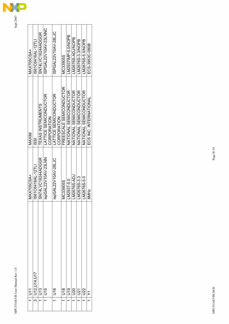
MPC
5516
EVB
Use
r Man
ual R
ev 1
.0
S
ept 2
007
1
U11
MA
X70
5CS
A+
MA
XIM
M
AX
705C
SA+
3
U
12,U
14,U
17IS
61C
6416
AL-1
2TLI
ISS
I IS
61C
6416
AL-1
2TLI
1
U13
S
N74
LVC
1624
4AD
GG
RTE
XA
S IN
STR
UM
ENTS
SN
74LV
C16
244A
DG
GR
1
U15
ispG
AL2
2V10
AV
-23L
NN
LA
TTIC
E SE
MIC
ON
DU
CTO
R
CO
RP
OR
ATI
ON
IS
PG
AL2
2V10
AV
-23L
NN
C
1
U
16is
pGA
L22V
10A
V-2
8LJC
LATT
ICE
SEM
ICO
ND
UC
TOR
C
OR
PO
RA
TIO
N
ISP
GA
L22V
10A
V-2
8LJC
1
U18
MC
3390
5SFR
EE
SC
ALE
SE
MIC
ON
DU
CTO
R
MC
3390
5S1
U
19LM
2937
-5.0
NAT
ION
AL
SE
MIC
ON
DU
CTO
R
LM29
37IM
P-5
.0/N
OP
B1
U
20LM
2676
S-AD
JN
ATIO
NAL
SE
MIC
ON
DU
CTO
RLM
2676
S-A
DJ/
NO
PB
1
U
21LM
2676
S-3
.3
NAT
ION
AL
SEM
ICO
ND
UC
TOR
LM26
76S-
3.3/
NO
PB1
U22
LM26
76S
-5.0
NAT
ION
AL
SEM
ICO
ND
UC
TOR
LM26
76S-
5.0/
NO
PB1
Y1
8MH
z E
CS
INC
. IN
TER
NA
TIO
NA
L E
CS
-395
3C-0
80B
MPC
5516
EVB
UM
/D
Page
B-1
9
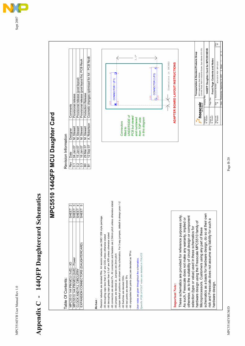
MPC
5516
EVB
Use
r Man
ual R
ev 1
.0
S
ept 2
007
- All
deco
uplin
g ca
ps le
ss th
an 0
.1uF
are
CO
G u
nles
s ot
herw
ise
stat
ed
- All
unpo
pula
ted
test
poi
nts
(via
s) a
re d
enot
ed a
s TP
Vx
- All
test
poi
nts
are
deno
ted
TPx
Spe
cific
PC
B L
AY
OU
T no
tes
are
deta
iled
in IT
ALI
CS
Use
r not
es a
re g
iven
thro
ught
out t
he s
chem
atic
s.
- Jum
per d
efau
lt po
sitio
ns a
re s
how
n in
the
sche
mat
ics.
For
3 w
ay ju
mpe
rs, d
efau
lt is
alw
ays
posn
1-2
- All
deco
uplin
g ca
ps g
reat
er th
an 0
.1uF
are
X7R
unl
ess
othe
rwis
e st
ated
- All
conn
ecto
rs a
re d
enot
ed P
x. A
ll co
nnec
tors
and
hea
ders
are
2.5
4mm
pitc
h un
less
oth
erw
ise
stat
ed- A
ll ju
mpe
rs a
re d
enot
ed J
x. J
umpe
rs a
re 2
mm
pitc
h
Notes:
- Res
isto
r net
wor
ks a
re d
onat
ed R
Nx.
All
resi
stor
net
wor
ks a
re S
MD
120
6 st
yle
pack
age.
- All
Sw
itche
s ar
e de
note
d S
Wx
MPC
5510
144
QFP
MC
U D
augh
ter C
ard
Dra
win
g Ti
tle:
Size
Doc
umen
t N
umbe
rR
ev
Dat
e:S
heet
of
Page
Titl
e:
Des
igne
r:
Dra
wn b
y:
Appr
oved
:
Tran
spor
tatio
n &
Sta
ndar
d Pr
oduc
ts G
roup
MC
D A
pplic
atio
ns E
ast
Kilb
ride
Col
ville
s R
oad,
Kel
vin
Ind
ustr
ial E
stat
e, E
ast K
ilbrid
e G
75 0
TG
SCH
-231
31 P
DF:
SPF
-231
31B
1
144Q
FP D
augh
ter C
ard
for M
PC55
10EV
B
B
Wed
nesd
ay,
Sept
embe
r 12,
200
7
Fron
t Pag
e Co
nten
ts a
nd N
otes
M. S
tewa
rt
M. S
tewa
rt
M. S
tewa
rt
15
04 J
an 0
7P
rovi
sion
al re
leas
e
Rev
isio
n In
form
atio
nD
esig
ner
0.1
Dat
eC
omm
ents
M. S
tew
art
B0
29 M
ar 0
7
Rev
Pro
visi
onal
rele
ase
(pos
t lay
out f
ix).
PC
B R
evA
M. S
tew
art
Pro
duct
ion
Rel
ease
0.
316
Jan
07
A. R
ober
tson
M. S
tew
art
M. S
tew
art
B1
Pro
visi
onal
rele
ase
(pos
t lay
out)
0.2
15 J
an 0
7
12 S
ep 0
7C
osm
etic
cha
nges
opt
imis
ed fo
r A4
- PC
B R
evB
CO
NN
EC
TOR
1 (P
1)12
CO
NN
EC
TOR
2 (P
2)
119
3.5"
2
0.2"119
1
120
120
Tabl
e O
f Con
tent
s:
EX
PA
NS
ION
CO
NN
EC
TOR
S (D
AU
GH
TER
CA
RD
)
SH
EE
T 2
Dimensions in INCHES
SH
EE
T 3
CLO
CK
AN
D P
LL C
IRC
UIT
RY
SH
EE
T 4
SH
EE
T 5
ADAP
TER
BO
ARD
LAY
OU
T IN
STR
UC
TIO
NS
MP
C55
10 1
44 P
IN M
CU
(1of
2) -
I/O
Thes
e sc
hem
atic
s ar
e pr
ovid
ed fo
r ref
eren
ce p
urpo
ses
only
.A
s su
ch, F
rees
cale
doe
s no
t mak
e an
y w
arra
nty,
impl
ied
orot
herw
ise,
as
to th
e su
itabi
lity
of c
ircui
t des
ign
or c
ompo
nent
sele
ctio
n (ty
pe o
r val
ue) u
sed
in th
ese
sche
mat
ics
for
hard
war
e de
sign
usi
ng th
e Fr
eesc
ale
MP
C55
10 fa
mily
of
Mic
ropr
oces
sors
. Cus
tom
ers
usin
g an
y pa
rt of
thes
esc
hem
atic
s as
a b
asis
for h
ardw
are
desi
gn, d
o so
at t
heir
own
risk
and
Free
scal
e do
es n
ot a
ssum
e an
y lia
bilit
y fo
r suc
h a
hard
war
e de
sign
.
Con
nect
ors
fitte
d to
UN
DE
RS
IDE
of
PC
B b
ut v
iewe
dan
d nu
mbe
red
from
TO
P s
ide
in th
is d
iagr
am
MP
C55
10 1
44 P
IN M
CU
(2of
2) -
Pow
er
Impo
rtan
t Not
e:
App
endi
x C
-
144Q
FP D
augh
terc
ard
Sche
mat
ics
MPC
5516
EVB
UM
/D
Page
B-2
0

MPC
5516
EVB
Use
r Man
ual R
ev 1
.0
S
ept 2
007
R2
0 O
HM
MPC551
6 14
4 LQ
FP M
CUPa
rt 1
of2
- I/
O Pi
ns NEXUS Port Controller
U1A
MP
C55
16_S
KT1
44
PA0
/ A
N0
9
PA1
/ A
N1
8
PA2
/ A
N2
7
PA3
/ A
N3
6
PA4
/ A
N4
5
PA5
/ A
N5
4
PA6
/ A
N6
3
PA7
/ A
N7
2
PA8
/ A
N8
143
PA9
/ A
N9
142
PA1
0 /
AN
1014
0
PA1
1 /
AN
1113
9
PA1
2 /
AN
1213
8
PA1
3 /
AN
1313
7
PA1
4 /
PA1
4 /
EXT
AL3
213
6
PA1
5 /
AN
15 /
XTA
L32
135
PB0
/ A
N28
/ e
MIO
S[1
6] /
PC
S_C
[5]
134
PB1
/AN
29 /
eM
IOS
[17]
/ P
CS
_C[4
]13
3
PB2
/ A
N30
/ e
MIO
S[1
8] /
PC
S_C
[3]
132
PB3
/ A
N31
/ P
CS_
C[2
]13
1
PB4
/ A
N32
/ P
CS_
C[1
]13
0
PB5
/ A
N33
/ P
CS_
C[0
]12
9
PB6
/ A
N34
/ S
CK_
C12
8
PB7
/ A
N35
/ S
OU
T_C
127
PB8
/ A
N36
/ S
IN_C
126
PB9
/ A
N37
/ C
NTX
_D /
PC
S_B
[4]
125
PB1
0 /
AN
38 /
CN
RX_
D /
PC
S_B
[3]
124
PB1
1 /
AN
39 /
eM
IOS
[19]
/ P
CS
_B[5
]12
3
eMIO
S[5]
/ P
CS_
A[2
] / P
E0
86
eMIO
S[4]
/ P
CS_
A[1
] / P
E1
85
eMIO
S[3]
/ P
CS_
A[0
] / P
E2
84
eMIO
S[2
] / S
CK
_A /
PE
383
eMIO
S[1]
/ S
OU
T_A
/ P
E4
82
eMIO
S[0
] / S
IN_A
/ P
E5
81
CLK
OU
T / P
E6
67
MS
EO /
AD
[8]
/ PF
264
MC
KO /
AD
[9]
/ PF
363
MD
O[0
] / A
D[1
0] /
PF
459
MD
O[1
] / A
D[1
1] /
PF
558
MD
O[2
] / A
D[1
2] /
PF
657
MD
O[3
] / A
D[1
3] /
PF
756
MD
O[4
] / A
D[1
4] /
PF
855
MD
O[5
] / A
D[1
5] /
PF
954
MD
O[6
] /
TXD
_C /
CS
[1] /
PF
1052
MD
O[7
] / R
XD_C
/ C
S[0
] / P
F11
51
TXD
_D /
TS
/ P
F12
50
RXD
_R /
OE
/ P
F13
49
CN
TX_D
/ B
DIP
/ W
E[0
] / P
F14
45
CN
RX_
D /
TE
A /
WE
[1] /
PF1
544
eMIO
S[1
6] /
AD
[16]
/ P
G0
43
SIN
_C /
eM
IOS
[17]
/ A
D[1
7] /
PG
142
SOU
T_C
/ e
MIO
S[1
8] /
AD
[18]
/ P
G2
41
SC
K_C
/ eM
IOS
[19]
/ A
D[1
9] /
PG
340
PC
S_C
[0]/
eM
IOS
[20]
/ A
D[2
0]/P
G4
39
eMIO
S[2
1] /
AD
[21]
/ P
G5
38
eMIO
S[2
2] /
AD
[22]
/ P
G6
37
RXD
_C /
eM
IOS
[23]
/ A
D[2
3] /
PG
736
SCL_
A /
eMIO
S[2
0] /
AN
[27]
/ P
H0
24
SD
A_A
/ e
MIO
S[2
1] /
AN
[26]
/ P
H1
23
eMIO
S[2
2] /
AN
[25]
/ P
H2
22
eMIO
S[2
3] /
AN
[24]
/ P
H3
21
MA[
2] /
TXD
_E /
AN
[23]
/ P
H4
20
MA[
1] /
RXD
_E /
AN
[22]
/ P
H5
19
TXD
_F /
AN
[21]
/ P
H6
18
RXD
_F /
AN
[20]
/ P
H7
17
MA
[0]
/ CN
TX_E
/ A
N[1
9] /
PH
814
CN
RX_
E /
AN
[18]
/ P
H9
13
CN
RX_
F /
AN
[17]
/ P
H10
12
CN
TX_F
/ A
N[1
6] /
PH
1111
PC
0 /
EMIO
S[0]
/ F
R_A
_TX_
EN /
AD
[24]
122
PC
1 /
EMIO
S[1]
/ F
R_A
_TX
/ A
D[1
6]12
1
PC
2 /
EMIO
S[2]
/ F
R_A
_RX
/ TS
120
PC
3 /
EMIO
S[3]
/ F
R_D
BG
011
7
PC
4 /
EMIO
S[4]
/ F
R_D
BG
111
6
PC
5 /
EMIO
S[5]
/ F
R_D
BG
211
5
PC
6 /
EMIO
S[6]
/ F
R_D
BG
311
4
PC
8 /
EMIO
S[8]
/ F
R_B
_TX
/ A
D[1
5]11
2
PC
9 /
EMIO
S[9]
/ F
R_B
_TX_
EN /
AD
[14]
111
PC
10 /
EM
IOS[
10]
/ PC
S_C
[5]
110
PC
7 /
EMIO
S[7]
/ F
R_B
_RX
113
PC
11 /
EM
IOS[
11]
/ PC
S_C
[4]
109
PC
12 /
EM
IOS[
12]
/ PC
S_C
[3]
108
PC
13 /
EM
IOS[
13]
/ PC
S_A
[5]
107
PC
14 /
EM
IOS[
14]
/ PC
S_A
[4]
106
PC
15 /
EM
IOS[
15]
/ PC
S_A
[3]
105
PD
0 /C
NTX
_A10
4
PD
1 /
CN
RX_
A10
3
PD
2 /
CN
RX_
B /
eMIO
S[1
0]10
2
PD
3 /
CN
TX_B
/ e
MIO
S[1
1]10
1
PD
4 /
CN
TX_C
/ eM
IOS[
12]
100
PD
5 /
CN
RX_
C /
eM
IOS
[13]
99
PD
6 /
TXD
_A /
eMIO
S[14
]98
PD
7 /
RXD
_A /
eM
IOS
[15]
97
PD
8 /
TXD
_B/ S
CL_
A94
PD
9 /
RXD
_B /
SD
A_A
93
PD
10 /
PC
S_B
[2]
/ CN
TX_F
/ Z
1_N
MI
92
PD
11 /
PC
S_B
[1]
/ CN
RX_
F /
Z0_
NM
I91
PD
12 /
PC
S_B
[0]
/ eM
IOS[
9]90
PD
13 /
SC
K_B
/ e
MIO
S[8
]89
PD
14 /
SO
UT_
B/ e
MIO
S[7
]88
PD
15 /
SIN
_B /
eM
IOS
[6]
87
PCS_
A[4
] / A
D[2
4] /
PG
835
TXD
_C /
PC
S_A
[3]
/ AD
[25]
/ P
G9
34
PCS_
A[2
] / A
D[2
6] /
PG
1030
PCS_
A[1
] / A
D[2
7] /
PG
1129
PCS_
A[0
] / A
D[2
8] /
PG
1228
SC
K_A
/ A
D[2
9] /
PG
1327
SOU
T_A
/ A
D[3
0] /
PG
1426
SIN
_A /
AD
[31]
/ P
G15
25
RE
SET
10
TDO
70
TDI
69
TMS
72
TCLK
71
JCO
MP
68
TES
T62
EVTI
/ R
D_W
R /
PF
066
EVTO
/ T
A /
PF
165
EXT
AL
75XT
AL
74
TP6
PF12
PD[0
..15
]
PB[0
..11]
PF13
PF14
PF15
PF1
PF2
PF3
PF0
PF4
PF5
PF8
PF9
MPC
5510
144Q
FP M
CU
IO
PG13
PF6
PF7
PF[
0..1
5]
PG2
PF10
PF11
PG12
PG14
PG15
PG0
PG1
PG3
PG4
PG5
PG6
PG7
PG9
PG10
PG11
PH1
PH2
PG
[0..1
5]
PG8
PH0
PH4
PH3
PH
[0..1
1]
PH8
PH9
PE3
PH5
PH6
PH7
PE5
PH10
PH11
PE0
PE4
MC
U-C
LKO
UT
PE[
0..6
]
PE1
TDI
TMS
TES
T
TCLK
JCO
MP
MC
U-R
STx
PB
7
PA[0
..15]
PB
0P
B1
PB
3P
B4
PB
5P
B6
PB
9P
B10
PB
11
PB
2
PC
1P
C2
PC
3
PB
8
PC
7P
C8
PA
0
PC
0
PC
13
PC
4P
C5
PC
6
PC
9P
C10
PC
11P
C12
PC
14P
C15
PD
0
PD
2P
D3
PD
4P
D5
PD
8P
D9
PD
10
PD
1
PD
15
PA
1
PD
6P
D7
PD
11P
D12
PD
13P
D14
PA
2
MC
U-X
TAL
PA
3
MC
U-E
XTA
L
PA
5P
A6
PA
7
TDO
PA
8P
A9
PA
10
PA
4
PA
12P
A13
MC
U-E
XTA
L32
MC
U-X
TAL3
2
PA
11
PE2
PC[0
..15
]
MC
U-E
XTAL
324
GN
D
PF[
0..1
5]5
PD
[0..
15]
5
PB
[0..1
1]5
MC
U-X
TAL3
24
PH
[0..1
1]5
MC
U-C
LKO
UT
4
PG
[0..1
5]5
TCLK
5
MC
U-X
TAL
4
PE[
0..6
]4,
5
MC
U-E
XTAL
4
TMS
5TD
I5
TDO
5
PA
[0..1
5]4,
5
JCO
MP
5
PC
[0..
15]
5
MC
U-R
STx
5D
raw
ing
Title
:
Size
Doc
umen
t Num
ber
Rev
Dat
e:S
heet
of
Page
Titl
e:
B1
144Q
FP D
augh
ter C
ard
for M
PC55
10EV
B
B
Wed
nesd
ay,
Sept
embe
r 12
, 20
07
MC
U Pa
ge 1
/2 (I
/O)
25
SC
H-2
3131
PD
F: S
PF-2
3131
MPC
5516
EVB
UM
/D
Page
B-2
1
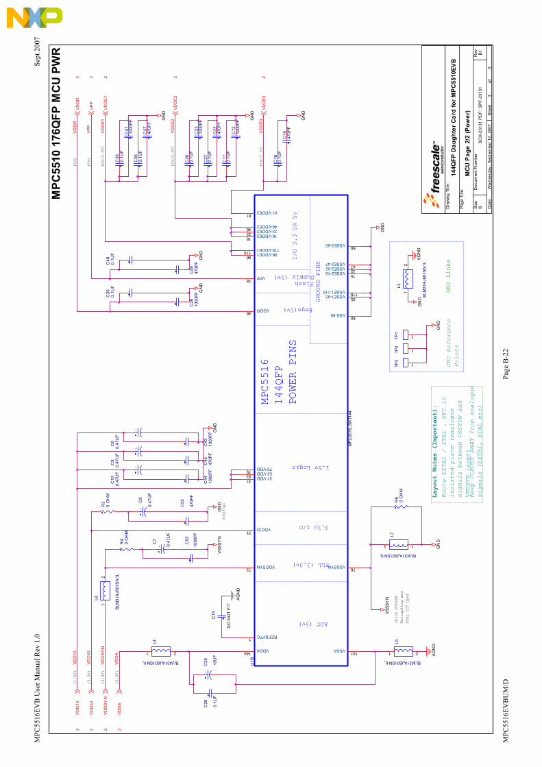
MPC
5516
EVB
Use
r Man
ual R
ev 1
.0
S
ept 2
007
(5V/3.3V)
(5V)
(VSS33a)
(3.3V)
GND Links
(5V/3.3V)
(5V/3.3V)
(1.5V)
(3.3V)
(5V)
(5.0V)
(From VDDS
YNDecoupling
and
XTAL CCT C
ps)
GND Reference
Points
Layout Notes (Important):
Route EXTAL / XTAL . XFC in
isolated plane (analogue
signals between VSSSYN and
VDDSYN layer)
Keep CLKOUT AWAY from analogue
signals (EXTAL, XTAL etc)
C52
470P
F
TP1 1
L4
BLM31AJ601SN1L
1 2C
380.
1UF
C26
0.1U
F
L6
BLM
31A
J601
SN
1L
12
C53
1000
PF
+C
8
0.47
UF
C29
1000
PF
C41
1000
PF
+C
25 10U
F
C30
0.1U
F
C36
0.1U
F
+C
7
0.47
UF
C45
470P
FC
15
DO
NO
T F
IT
L5
BLM31AJ601SN1L
1 2
C37
470P
F
+
C9
0.47
UF
C43
1000
PF
MPC5516
ADC (5v)
Regs(5v)
Flash
PLL (3.3v)
3.3v I/O
1.5v Logic
144QFP
POWER PINS
I/O 3.3 OR 5v
GROUND PINS
Supply (5v)
U1B
MP
C55
16_S
KT1
44
VDD3377
VDDSYN73
VSS-8080
VSSA141
VSSSYN76
VDDR46
96-VDDE196
31-VDD31
53-VDD53
VDDA144
VPP78
79-VDD79
REFBYPC1
16-VDDE216
119-VDDE1119
33-VDDE233
48-VDDE248
61-VDDE361
VSSE1-9595
VSSE1-118118
VSSE2-1515
VSSE2-3232
VSSE3-6060
VSSE2-4747
C28
0.1U
F
C48
0.1U
F
C44
1000
PF
C11
0.1U
F
+
C6
0.47
UF
L7
BLM31AJ601SN1L
12
R6
0 O
HM
C12
1000
PF
R3
0 O
HM
+
C10
0.47
UF
C49
470P
F
L2
BLM
31A
J601
SN
1L
12
C18
0.1U
F
C27
0.1U
F
R4
0 O
HM
TP3 1
C23
1000
PF
C22
470P
F
TP2 1
C19
470P
F
MPC
5510
176
QFP
MC
U P
WR
VD
DS
YN
VD
DE
2
VD
DE
1
VD
DR
Dra
wing
Titl
e:
Size
Doc
umen
t N
umbe
rR
ev
Dat
e:S
heet
of
Pag
e Ti
tle:
B1
144Q
FP D
augh
ter C
ard
for
MPC
5510
EVB
B
Wed
nesd
ay,
Sep
tem
ber
12,
2007
MC
U P
age
2/2
(Pow
er)
35
SC
H-2
3131
PD
F:
SP
F-2
3131
VP
P
VD
D15
VD
DA
VD
DE
3
VD
D33
VS
SS
YN
AG
ND
GN
D
GN
D
GN
D
GN
D
GN
D
GN
D
GN
D
GN
D
VS
SS
YN
AG
ND
GN
D
GN
D
GN
D
AG
ND
VD
DE
22
VD
DS
YN
2
VP
P2
VD
DE
12
VD
DA
2
VD
DE
32
VD
DR
2V
DD
152
VD
D33
2
MPC
5516
EVB
UM
/D
Page
B-2
2

MPC
5516
EVB
Use
r Man
ual R
ev 1
.0
S
ept 2
007
FID
5FI
D6
FID
8
FID
1FI
D2
FID
3FI
D4
FID
7
MC
U-X
TAL
2M
CU
-XTA
L(M
CU Cry
stal O
utput)
J11
2
3
J2
1
2
3
J41
2
3
Dra
wing
Titl
e:
Size
Doc
umen
t Num
ber
Rev
Dat
e:Sh
eet
of
Pag
e Ti
tle:
B1
144Q
FP D
augh
ter C
ard
for M
PC55
10EV
B
B
Wed
nesd
ay, S
epte
mbe
r 12,
200
7
Cloc
k Ci
rcui
try
45
SCH
-231
31 P
DF
: SP
F-23
131
J31
2
3
Keep MCU-CLKOUT AWAY from
analoguesignals (EXTAL, XTAL etc)
Route EXTAL / XTAL in isolated
plane (analogue signals between
VSSSYN and VDDSYN layer)
Layout Notes (Important):
MC
U-E
XTAL
2M
CU
-EXT
AL
(MCU
Cry
stal I
nput)
GN
D
(FRO
M Ex
pansio
nCo
nnecto
rs)
EVB-
EXTA
L5
(MCU
32K
Hz EXT
AL)
GN
D
EXTA
L
Loop Controlled Pierce
Oscillator Circuit
Place resistor as close as
possible to MCU CLKOUT pin
C54
33PF
PE6
C55
33PF
R7
33.0
OH
M
J51
2
Y2
8MH
z
12
VSS
SYN
32Khz Oscillator Circuit
MC
U-X
TAL3
2
MC
U-E
XTA
L32
MC
U-C
LKO
UT
C31
10PF
C24
10PF
EXT
AL3
2
Y1
32.7
68K
Hz
12
MC
U-E
XTAL
322
PA[0
..15
]2,
5
MC
U-X
TAL3
22
PA1
4
(MCU
32K
Hz X
pans
ion
Conn
TAL)
(TO
Exec
tors)
PA[0
..15
]
PE[0
..6]
CLO
CK
CIR
CU
ITR
Y
PA1
5
R5
0 O
HM
Connect XTAL jumper to GND when driving EXTAL from
Oscilaltor Module or External Source (PLL Bypass
Mode)
MC
U-C
LKO
UT
2
PE[0
..6]
2,5
(FRO
M MC
U)
XTAL
XTAL
32
(TO
Expans
ion Co
nnecto
rs)
REMOVE XTAL jumper when driving EXTAL from
Oscilaltor Module or External Source (PLL Enabled)
EVB
-EXT
AL
MPC
5516
EVB
UM
/D
Page
B-2
3
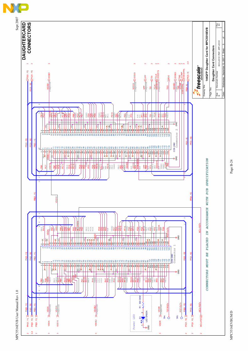
MPC
5516
EVB
Use
r Man
ual R
ev 1
.0
S
ept 2
007
GND
PA[
0..1
5]
GND
GND
GND
PB[
0..1
1]
DA
UGHT
ERC
AR
D
CO
NNEC
TOR
S
CONNECTORS MUST BE PLACED IN ACCORDANCE WITH PCB SPECIFICATION
PH
[0..1
1]
GND
Dra
win
g Ti
tle:
Size
Doc
umen
t N
umbe
rR
ev
Dat
e:Sh
eet
of
Page
Titl
e:
B1
144Q
FP D
augh
ter C
ard
for M
PC55
10EV
B
B
Wed
nesd
ay, S
epte
mbe
r 12
, 20
07
Daug
hter
Car
d Co
nnec
tors
55
SC
H-2
3131
PD
F: S
PF-2
3131
GND
PF[0
..15]
GND
PG
[0..1
5]
GND
GND
MC
U-R
STx
2
GND
PF[
0..1
5]
GND
PF[
0..1
5]
GND
J6 CO
N 2
X60
11
33
55
77
99
1111
1313
1515
1717
1919
2121
2323
2525
2727
2929
3131
3333
3535
3737
3939
4141
4343
4545
4747
4949
5151
5353
5555
5757
5959
6161
6363
6565
6767
6969
7171
7373
7575
7777
7979
8181
8383
8585
8787
8989
9191
9393
9595
9797
9999
101
101
103
103
105
105
107
107
109
109
111
111
113
113
115
115
117
117
119
119
22
44
66
88
1010
1212
1414
1616
1818
2020
2222
2424
2626
2828
3030
3232
3434
3636
3838
4040
4242
4444
4646
4848
5050
5252
5454
5656
5858
6060
6262
6464
6666
6868
7070
7272
7474
7676
7878
8080
8282
8484
8686
8888
9090
9292
9494
9696
9898
100
100
102
102
104
104
106
106
108
108
110
110
112
112
114
114
116
116
118
118
120
120
D1
LED
GR
EEN2
1
J7
CO
N 2
X60
11
33
55
77
99
1111
1313
1515
1717
1919
2121
2323
2525
2727
2929
3131
3333
3535
3737
3939
4141
4343
4545
4747
4949
5151
5353
5555
5757
5959
6161
6363
6565
6767
6969
7171
7373
7575
7777
7979
8181
8383
8585
8787
8989
9191
9393
9595
9797
9999
101
101
103
103
105
105
107
107
109
109
111
111
113
113
115
115
117
117
119
119
22
44
66
88
1010
1212
1414
1616
1818
2020
2222
2424
2626
2828
3030
3232
3434
3636
3838
4040
4242
4444
4646
4848
5050
5252
5454
5656
5858
6060
6262
6464
6666
6868
7070
7272
7474
7676
7878
8080
8282
8484
8686
8888
9090
9292
9494
9696
9898
100
100
102
102
104
104
106
106
108
108
110
110
112
112
114
114
116
116
118
118
120
120
R1
560
OH
M
TP4
TP5
VDD
15
PE5
EVB
-EXT
AL
RST
-OU
Tx
VDD
AVD
DA
VDD
E2VD
DA
VDD
R
RS
T-O
UTx
PB2
PA8
PB3
PA12
PB4
PA14
PA1
3
PA1
PA15
PA6
PB5
PA4
PA1
0
PH11
PH9
PH7
PH4
PG14
PF8
PF12
PH10
PG0
PF13
PH0
PG12
PG4
PG10
PF7
PF14
PG2
PG5
PF9
PG1
PA1
1P
A9P
A7P
B1
MC
U-R
STx
MC
U-R
STx
PA0
PB0
PH
3
PA3
PA5
MC
U-R
STx
PA2
PH
8P
H5
PH
6
PG
13P
G15
PF1
5
PG
9
PG
3
PG
8
PH
1P
H2
PG
6
VD
DR
PG
11P
F11
PF1
0
PG
7
PF6
VDD
E1
VD
D15
VD
D15
VDD
E1
VPP
VPP
VPP
VDD
SYN
PB7
PC0
PC5
VDD
SYN
PB6
PC7
PC8
VD
D15
PC11
PC14
PC6
PD0
PD2
PD9
PD10
PD14
PC13
PE4
VDD
33
PD3
PD6
PE2
PE3
EVB
-EXT
AL
VDD
33
PE6
PF2
JCO
MP
JCO
MP
TMS
PB10
PC3
VDD
E3
PC12
TMS
PB9
PC10
PB11
PC4
PB8
PC1
PC9
PD1
PD4
PD5
PD7
PD15
PE1
PC2
PC15
PF5
PD8
PD12
PD13
VDD
E3
PF0
PF1
TCLK
TCLK
PF4
PF3
TDO
PB[
0..1
1]
TDI
TDI
TDO
PB[
0..1
1]
PC[0
..15
]
PH[0
..11
]
PE[0
..6]
PC
[0..1
5]
PD
[0..1
5]
VDD
E2
PF[0
..15]
PG[0
..15
]PE
[0..6
]
PA[0
..15]
PD11
PB[0
..11]
PE0
TGT-
RST
x
VDD
15
GN
D
GN
DG
ND
GN
D
VD
DA
3
PA[0
..15]
2,4
EVB
-EXT
AL4
GN
D
VD
DR
3
PB[0
..11]
2
VD
DSY
N3
VPP
3
VDD
153
VD
DE
23
VD
DE3
3
VD
DE1
3
TCLK
2
TDO
2
VD
D33
3
JCO
MP
2
PF[0
..15]
2
TMS
2
TDI
2
PE[0
..6]
2,4
PH[0
..11]
2
PG[0
..15]
2
PC[0
..15]
2
PD[0
..15]
2
PE14
pered)
PK0
mpered
)
mper
VDDE2
VDDE
VDDE
2
(NC)
mpered
)
mper
VDDE
2
VDDE
2
VDD1
5VD
D1
VDD1
5
(NC)
VD
VDDE
1
VDDE
1
VDDE
1
VDD1
5
VDD1
5
VDVDDE
1
VDD1
5
pere
pered)
VDDE
3
pere
PK1
PH13
pered)
VDD1
5
PE10
PJ9
PJ3
PE7
PJ5
PE9
PE15
PJ4
PH15
PH14
PJ2
PJ6
PB15
PB14
PJ1
PE11
GND
GND
Connector 1
(Jum
GND
GND
GND
(Ju
(NC)
(NC)
GND
GND
GND
GND
GND
(Ju
ed)
VDDE2
GND
GND
GND
2
(NC)
(NC)
(Ju
(Ju
ed)
VDDE
2
GND
VDD1
5
5
VDD15
Conenctor 2
GND
BK
K
(NC)
(NC)
H
G
BA
A
DE1
H
GF
VDDE
1
VDDE
1
F
VDDE
1
D
D15
VDD1
5
EBC
VDDE
3
CD
(Jum
d)
(Jum
GND
B
(Jum
d)
F
VDDE
3
EF
(Jum
PB13
PB12
PJ11
PJ12
PE12
PJ10 PJ
7
PH12
PJ13
PE8
PE13
PJ0
Power LED
VDD15
PJ14
PJ15
PJ8
GND
MPC
5516
EVB
UM
/D
Page
B-2
4

MPC
5516
EVB
Use
r Man
ual R
ev 1
.0
S
ept 2
007
App
endi
x D
-
144Q
FP D
augh
terc
ard
Bill
Of M
ater
ials
Qty
Ref
des
Valu
e M
anuf
actu
rer
Part
Num
ber
5
C6,
C7,
C8,
C9,
C10
0.47
UF
AV
X
TAJA
474M
025R
10
C
11,C
15,C
18,C
26,C
27,C
28,C
30,C
36,C
38,C
480.
1UF
MU
RA
TAG
RM
188R
71H
104K
A93
D7
C
12,C
23,C
29,C
41,C
43,C
44,C
53
1000
PF
VE
NK
EL
CO
MP
AN
Y
C08
05C
OG
500-
102J
NE
6
C19
,C22
,C37
,C45
,C49
,C52
47
0PF
PA
NA
SO
NIC
E
CJ1
VC1H
471J
2
C24
,C31
10
PF
KE
ME
T C
0603
C10
0F5G
AC
1
C25
10
UF
VIS
HA
Y IN
TER
TEC
HN
OLO
GY
293D
106X
9010
A2T
E3
2
C
54,C
5533
PF
VE
NK
EL
CO
MP
AN
Y
C06
03C
0G50
0-33
0JN
E
1 D
1 LE
D G
RE
EN
K
ING
BR
IGH
T K
/AP
T-32
16SG
D
8
FID
1,FI
D2,
FID
3,FI
D4,
FID
5,FI
D6,
FID
7,FI
D8
FID
-040
GE
NE
RIC
FID
-040
4
J1
,J2,
J3,J
4 H
DR
3X
1S
AM
TEC
TMM
-103
-02-
G-S
1
J5
H
DR
1X
2S
AM
TEC
TM
M-1
02-0
2-G
-S2
J6,J
7 C
ON
2X
60
TYC
O E
LEC
TRO
NIC
S
5-51
7900
9-5
5
L2
,L4,
L5,L
6,L7
B
LM31
AJ6
01S
N1L
MU
RA
TA
BLM
31A
J601
SN
1L1
R1
560
OH
M
KO
A S
PE
ER
R
K73
H1J
TTD
5600
F 5
R2,
R3,
R4,
R5,
R6
0 O
HM
TH
YE
MIN
G T
EC
H C
O L
TD
CR
-03J
L7-0
R
MPC
5516
EVB
UM
/D
Page
B-2
5

MPC
5516
EVB
Use
r Man
ual R
ev 1
.0
S
ept 2
007
- All
deco
uplin
g ca
ps le
ss th
an 0
.1uF
are
CO
G u
nles
s ot
herw
ise
stat
ed
- All
unpo
pula
ted
test
poi
nts
(via
s) a
re d
enot
ed a
s TP
Vx
- All
test
poi
nts
are
deno
ted
TPx
Spe
cific
PC
B L
AY
OU
T no
tes
are
deta
iled
in IT
ALI
CS
Use
r not
es a
re g
iven
thro
ught
out t
he s
chem
atic
s.
- Jum
per d
efau
lt po
sitio
ns a
re s
how
n in
the
sche
mat
ics.
For
3 w
ay ju
mpe
rs, d
efau
lt is
alw
ays
posn
1-2
- All
deco
uplin
g ca
ps g
reat
er th
an 0
.1uF
are
X7R
unl
ess
othe
rwis
e st
ated
- All
conn
ecto
rs a
re d
enot
ed P
x. A
ll co
nnec
tors
and
hea
ders
are
2.5
4mm
pitc
h un
less
oth
erw
ise
stat
ed- A
ll ju
mpe
rs a
re d
enot
ed J
x. J
umpe
rs a
re 2
mm
pitc
h
Notes:
- Res
isto
r net
wor
ks a
re d
onat
ed R
Nx.
All
resi
stor
net
wor
ks a
re S
MD
120
6 st
yle
pack
age.
- All
Sw
itche
s ar
e de
note
d S
Wx
C0
Pro
duct
ion
Rel
ease
- P
CB
Rev
CA
. Rob
erts
on12
Sep
t 07
MPC
5510
176
QFP
MC
U D
augh
ter C
ard
Dra
win
g Ti
tle:
Size
Doc
umen
t N
umbe
rR
ev
Dat
e:S
heet
of
Pag
e Ti
tle:
Des
igne
r:
Dra
wn
by:
App
rove
d:
Tran
spor
tatio
n &
Sta
ndar
d Pr
oduc
ts G
roup
MC
D A
pplic
atio
ns E
ast
Kilb
ride
Col
vill
es R
oad,
Kel
vin
Ind
ustr
ial E
stat
e, E
ast
Kilb
ride
G75
0TG
SC
H-2
3553
PD
F:
SPF
-235
53C
0
176Q
FP D
augh
ter C
ard
for M
PC55
10EV
B
B
Wed
nesd
ay,
Sept
embe
r 12
, 20
07
Fron
t Pag
e Co
nten
ts a
nd N
otes
A.
Rob
erts
on
A.
Rob
erts
on
A.
Rob
erts
on
15
CO
NN
EC
TOR
1 (P
1)12
CO
NN
EC
TOR
2 (P
2)
119
13 J
un 0
70.
1D
esig
ner
Rev
isio
n In
form
atio
n
3.5"
2
0.2"
Pro
toty
pe re
leas
e - P
CB
Rev
A
A. R
ober
tson
119
1
Com
men
ts 120
120
Dat
eTa
ble
Of C
onte
nts:
EX
PA
NS
ION
CO
NN
EC
TOR
S (D
AU
GH
TER
CA
RD
)
SH
EE
T 2
Dimensions in INCHES
SH
EE
T 3
CLO
CK
AN
D P
LL C
IRC
UIT
RY
SH
EE
T 4
SH
EE
T 5
Rev
AD
APTE
R B
OAR
D L
AYO
UT
INST
RU
CTI
ON
S
MP
C55
10 1
76 P
IN M
CU
(1of
2) -
I/O
Thes
e sc
hem
atic
s ar
e pr
ovid
ed fo
r ref
eren
ce p
urpo
ses
only
.A
s su
ch, F
rees
cale
doe
s no
t mak
e an
y w
arra
nty,
impl
ied
orot
herw
ise,
as
to th
e su
itabi
lity
of c
ircui
t des
ign
or c
ompo
nent
sele
ctio
n (ty
pe o
r val
ue) u
sed
in th
ese
sche
mat
ics
for
hard
war
e de
sign
usi
ng th
e Fr
eesc
ale
MP
C55
10 fa
mily
of
Mic
ropr
oces
sors
. Cus
tom
ers
usin
g an
y pa
rt of
thes
esc
hem
atic
s as
a b
asis
for h
ardw
are
desi
gn, d
o so
at t
heir
own
risk
and
Free
scal
e do
es n
ot a
ssum
e an
y lia
bilit
y fo
r suc
h a
hard
war
e de
sign
.
Con
nect
ors
fitte
d to
UN
DE
RS
IDE
of
PC
B b
ut v
iewe
dan
d nu
mbe
red
from
TO
P s
ide
in th
is d
iagr
am
MP
C55
10 1
76 P
IN M
CU
(2of
2) -
Pow
er
Impo
rtan
t Not
e:
20 A
ug 0
7B
2C
orre
ctio
n to
Clo
ck S
elec
tion
Jum
pers
A. R
ober
tson
15 A
ug 0
7B
1P
rodu
ctio
n R
elea
se -
PC
B R
evB
(Not
man
ufac
ture
d)A
. Rob
erts
on08
Aug
07
B0
Cor
rect
ion
to V
DD
E1
shor
tA
. Rob
erts
on
App
endi
x E
-
176Q
FP D
augh
terc
ard
Sche
mat
ics
MPC
5516
EVB
UM
/D
Page
B-2
6

MPC
5516
EVB
Use
r Man
ual R
ev 1
.0
S
ept 2
007
PJ[
4..1
5]5
PJ1
4P
J13
PJ1
2
PJ1
5
PJ[
4..1
5]
PJ7
PJ6
PJ5
PJ4
PJ1
1P
J10
PJ9
PJ8
Not available
on 176QFP
PH
13P
H12
PF
[0..
15]
5
TDI
PF
1P
F0
PF
15P
F14
PF
13P
F12
PF
3P
F2
PF
6P
F5
PF
4
PF
10P
F9
PF
8
PF
[0..
15]
PF
7
PF
11
PG
[0..
15]
5
PG
14P
G13
PG
12
TMS
PG
3P
G2
PG
1P
G0
PG
15
PG
4
PG
8
PG
[0..
15]
PG
7P
G6
PG
5
PD
[0..
15]
5
PG
11P
G10
PG
9
TCLK
JCO
MP
TCLK
5
MC
U-R
STx
TMS
5
MC
U-X
TAL
4
TES
T
MC
U-E
XTA
L32
4M
CU
-XTA
L32
4
TDI
5
MC
U-E
XTA
L32
PA
[0..
15]
MC
U-E
XTA
L4
PB
1P
B0
PB
[0..
15]
PB
7P
B6
PB
5P
B4
PB
3P
B2
PB
12P
B11
PB
10P
B9
PB
8
JCO
MP
5
MC
U-X
TAL3
2
PB
15P
B14
PB
13
PA
0
PC
2P
C1
PC
0
PC
[0..
15]
PC
7P
C6
PC
5P
C4
PC
3
PC
13P
C12
PC
11P
C10
PC
9P
C8
PC
15P
C14
PA
[0..
15]
5
R10
00
OH
M
PD
1P
D0
PD
[0..
15]
PD
6P
D5
PD
4P
D3
PD
2
PD
12P
D11
PD
10P
D9
PD
8P
D7
GN
D
PA
1
PD
15P
D14
PD
13
PA
3
MC
U-X
TAL
PA
2
PB
[0..
15]
3,5
MPC
5510
176Q
FP M
CU
IO
PC
[0..
15]
5
MC
U-E
XTA
L
TPV
6
Dra
win
g Ti
tle:
Siz
eD
ocum
ent
Num
ber
Rev
Dat
e:S
heet
of
Pag
e Ti
tle:
C0
176Q
FP D
augh
ter
Card
for M
PC55
10EV
B
B
Wed
nesd
ay,
Sep
tem
ber
12,
2007
MC
U P
age
1/2
(I/O
)
25
SC
H-2
3553
PD
F:
SP
F-2
3553
TPV
5
Not available
on 176QFP
Signals not available on 176 QFP
TP10
0
PA
5P
A4
PA
7P
A6
TDO
5TD
O
PA
8
PA
14P
A13
PA
12P
A11
PA
10P
A9
MC
U-R
STx
5
PA
15
PE
8P
E9
TPV
2
PE7, PE8, PE9
PE
12
MC
U-C
LKO
UT
4
PE
15P
E14
PE
13
PE
0
PE
2P
E1
PE
3
MC
U-C
LKO
UT
PE
5P
E4
PE
[0..
15]
4,5
PE
10
PE
[0..
15]
PE
11
TPV
4
PE
7
PH12, PH13
(PJ[0..3] not availble on 176QFP)
PJ0, PJ1. PJ2, PJ3
TPV
7
MPC5516 176QFP
I/O Pins
NEXUS Port Controller
U1A
MP
C55
16_S
KT1
76
PA
0/A
N0
9
PA
1/A
N1
8
PA
2/A
N2
7
PA
3/A
N3
6
PA
4/A
N4
5
PA
5/A
N5
4
PA
6/A
N6
3
PA
7/A
N7
2
PA
8/A
N8
175
PA
9/A
N9
174
PA
10/A
N10
172
PA
11/A
N11
171
PA
12/A
N12
170
PA
13/A
N13
169
PA
14 /
PA
14/E
XTA
L32
167
PA
15 /
AN
15/X
TAL3
216
5
PB
0/A
N28
/eM
IOS
[16]
/PC
S_C
[5]
162
PB
1/A
N29
/eM
IOS
[17]
/PC
S_C
[4]
161
PB
2/A
N30
/eM
IOS
[18]
/PC
S_C
[3]
160
PB
3/A
N31
/PC
S_C
[2]
159
PB
4/A
N32
/PC
S_C
[1]
158
PB
5/A
N33
/PC
S_C
[0]
157
PB
6/A
N34
/SC
K_C
156
PB
7/A
N35
/SO
UT_
C15
3
PB
8/A
N36
/SIN
_C15
2
PB
9/A
N37
/CN
TX_D
/PC
S_B
[4]
151
PB
10/A
N38
/CN
RX_
D/P
CS
_B[3
]15
0
PB
11/A
N39
/eM
IOS
[19]
/PC
S_B
[5]
149
PB
12/T
XD_G
/PC
S_B
[4]
164
PB
13/R
XD_G
/PC
S_B
[3]
163
PB
14/T
XD_H
148
PB
15/R
XD_H
147
MLB
CLK
/eM
IOS
[5]/
PC
S_A
[2]/
PE
010
6
MLB
SI/
eMIO
S[4
]/P
CS
_A[1
]/P
E1
103
MLB
DI/
eMIO
S[3
]/P
CS
_A[0
]/P
E2
101
MLB
SO
/eM
IOS
[2]/
SC
K_A
/PE
310
0
MLB
DO
/eM
IOS
[1]/
SO
UT_
A/P
E4
98
MLB
_SLO
T/eM
IOS
[0]/
SIN
_A/P
E5
97
CLK
OU
T/P
E6
83
MS
EO
/MLB
SI/
AD
[8]/
PF
280
MC
KO
/MLB
DI/
AD
[9]/
PF
379
MD
O[0
]/M
LBS
O/A
D[1
0]/P
F4
74
MD
O[1
]/M
LBD
O/A
D[1
1]/P
F5
72
MD
O[2
]/M
LB_S
LOT/
AD
[12]
/PF
668
MD
O[3
]/A
D[1
3]/P
F7
66
MD
O[4
]/A
D[1
4]/P
F8
65
MD
O[5
]/A
D[1
5]/P
F9
64
MD
O[6
]/TX
D_C
/CS
[1]/
PF
1062
MD
O[7
]/R
XD_C
/CS
[0]/
PF
1161
TXD
_D/T
S/P
F12
60
RXD
_D/O
E/P
F13
59
CN
TX_D
/BD
IP/W
E[0
]/P
F14
55
CN
RX_
D/T
EA
/WE
[1]/
PF
1554
eMIO
S[1
6]/A
D[1
6]/P
G0
51
SIN
_C/e
MIO
S[1
7]/A
D[1
7]/P
G1
50
SO
UT_
C/e
MIO
S[1
8]/A
D[1
8]/P
G2
49
SC
K_C
/eM
IOS
[19]
/AD
[19]
/PG
348
PC
S_C
[0]/
eMIO
S[2
0]/A
D[2
0]/P
G4
47
eMIO
S[2
1]/A
D[2
1]/P
G5
46
eMIO
S[2
2]/A
D[2
2]/P
G6
45
RXD
_C/e
MIO
S[2
3]/A
D[2
3]/P
G7
44
SC
L_A
/eM
IOS
[20]
/AN
[27]
/PH
032
SD
A_A
/eM
IOS
[21]
/AN
[26]
/PH
131
CS
[3]/
eMIO
S[2
2]/A
N[2
5]/P
H2
30
CS
[2]/
eMIO
S[2
3]/A
N[2
4]/P
H3
29
MA
[2]/
TXD
_E/A
N[2
3]/P
H4
28
MA
[1]/
RXD
_E/A
N[2
2]/P
H5
24
TXD
_F/A
N[2
1]/P
H6
23
RXD
_F/A
N[2
0]/P
H7
22
MA
[0]/
CN
TX_E
/AN
[19]
/PH
817
CN
RX_
E/A
N[1
8]/P
H9
14
CN
RX_
F/A
N[1
7]/P
H10
12
CN
TX_F
/AN
[16]
/PH
1111
PH
1453
PH
1552
PE
1011
2
PE
1111
1
PE
1210
9
PE
1310
8
PE
1410
2
PE
1599
PC
0/eM
IOS
[0]/
FR
_A_T
X_E
N14
6
PC
1/eM
IOS
[1]/
FR
_A_T
X14
5
PC
2/eM
IOS
[2]/
FR
_A_R
X14
4
PC
3/eM
IOS
[3]/
FR
_DB
G0
141
PC
4/eM
IOS
[4]/
FR
_DB
G1
140
PC
5/eM
IOS
[5]/
FR
_DB
G2
139
PC
6/eM
IOS
[6]/
FR
_DB
G3
138
PC
8/eM
IOS
[8]/
FR
_B_T
X13
6
PC
9/eM
IOS
[9]/
FR
_B_T
X_E
N13
5
PC
10/e
MIO
S[1
0]/P
CS
_C[5
]13
4
PC
7/eM
IOS
[7]/
FR
_B_R
X13
7
PC
11/e
MIO
S[1
1]/P
CS
_C[4
]13
3
PC
12/e
MIO
S[1
2]/P
CS
_C[3
]13
2
PC
13/e
MIO
S[1
3]/P
CS
_A[5
]13
1
PC
14/e
MIO
S[1
4]/P
CS
_A[4
]13
0
PC
15/e
MIO
S[1
5]/P
CS
_A[3
]12
9
PD
0/C
NTX
_A/P
CS
_D[3
]12
8
PD
1/C
NR
X_A
/PC
S_D
[4]
127
PD
2/C
NR
X_B
/eM
IOS
[10]
/BO
OTC
FG
126
PD
3/C
NTX
_B/e
MIO
S[1
1]12
5
PD
4/C
NTX
_C/e
MIO
S[1
2]12
4
PD
5/C
NR
X_C
/eM
IOS
[13]
123
PD
6/TX
D_A
/eM
IOS
[14]
122
PD
7/R
XD_A
/eM
IOS
[15]
121
PD
8/TX
D_B
/SC
L_A
118
PD
9/R
XD_B
/SD
A_A
117
PD
10/P
CS
_B[2
]/C
NTX
_F/N
MI0
116
PD
11/P
CS
_B[1
]/CN
RX_
F/N
MI1
115
PD
12/P
CS
_B[0
]/eM
IOS
[9]
114
PD
13/S
CK
_B/e
MIO
S[8
]11
3
PD
14/S
OU
T_B
/eM
IOS
[7]
110
PD
15/S
IN_B
/eM
IOS
[6]
107
PC
S_A
[4]/
AD
[24]
/PG
843
TXD
_C/P
CS
_A[3
]/A
D[2
5]/P
G9
42
PC
S_A
[2]/
AD
[26]
/PG
1038
PC
S_A
[1]/
AD
[27]
/PG
1137
PC
S_A
[0]/
AD
[28]
/PG
1236
SC
K_A
/AD
[29]
/PG
1335
SO
UT_
A/A
D[3
0]/P
G14
34
SIN
_A/A
D[3
1]/P
G15
33
PJ4
75
PJ5
73
PJ6
69
PJ7
67
PC
S_D
[4]/
PJ8
27
PC
S_D
[3]/
PJ9
26
PC
S_D
[2]/
PJ1
025
PC
S_D
[1]/
PJ1
119
PC
S_D
[0]/
PJ1
218
SC
K_D
/PJ1
316
SO
UT_
D/P
J14
15
SIN
_D/P
J15
13
PK
0/E
XTA
L32
168
PK
1/XT
AL3
216
6
RE
SE
T10
TDO
86
TDI
85
TMS
88
TCK
87
JCO
MP
84
VS
UP
/TE
ST
78
EV
TI/R
D_W
R/P
F0
82
EV
TO/M
LBC
LK/T
A/P
F1
81
EXT
AL/
EXT
CLK
91XT
AL
90
PH
[0..
15]
5
PH
1P
H0
PH
15P
H14
PH
3P
H2
PH
7P
H6
PH
5P
H4
PH
11P
H10
PH
9P
H8
PH
[0..
15]
MPC
5516
EVB
UM
/D
Page
B-2
7
MPC
5516
EVB
Use
r Man
ual R
ev 1
.0
S
ept 2
007
MPC
5516
EVB
UM
/D
Page
B-2
8
(5.0
V)
(5V)
VPP
GN
D
L103
BLM
31AJ
601S
N1L
12
+
C4
0.47
UF
+
C2
0.47
UF
GN
D
C10
547
0PF
C11
4
1000
PF
C10
2
0.1U
F
DO
NO
T F
IT
AGN
D
+
C43
0.47
UF
C12
1
470P
F
MPC551
6 17
6QFP
ADC (5v)
Regs
Flash
PLL
3.3v I/O
1.5v Logic
POWER PINS
I/O 3.3 OR 5v
GROUND PINS
Supply
(5v)
(5v)
(3.3v)
U1B
MPC
5516
_SKT
176
VFLASH/VDD3393
VDDSYN89
VSSE1-142 142VSSE1-119 119VSSE1-104104
VSSA/VRL 173
VSSSYN 92
VDDR56
95-VDD/VDDF95
39-VDD39
120-VDDE1120
VDDA/VRH176
VPP94
63-VDD63
REFBYPC1
143-VDDE1143
155-VDDE1155
21-VDDE221
105-VDDE1105
41-VDDE241
58-VDDE258
71-VDDE371
77-VDDE377
VSSE2-57 57VSSE2-4040VSSE2-2020
VSSE3-7676VSSE3-70 70
VSS/VSSF-9696
VSSE1-154 154
VD
D15
C10
4
0.1U
FC
103
470P
F
VD
DA
R10
10
OH
MR
102
0 O
HM
C10
60.
1UF
C1
1000
PF
C11
1
470P
F
C11
0
0.1U
F
GND Reference
Points
GN
D
GND Links
GN
D
L101
BLM
31AJ
601S
N1L
12
AGN
D
TP3 1
TP2 1
TP1 1
L102
BLM
31AJ
601S
N1L
1 2VD
DA
5
C11
8
0.1U
FC
115
470P
F
C11
6
0.1U
FC
117
1000
PF
VDD
335
C7
1000
PF
C12
0
0.1U
F
C12
3
0.1U
FC
124
470P
F
C11
2
0.1U
F
GN
D
C11
3
470P
F
VDD
E35
C127 1000PF
+
C128 0.47UF
(3.3
V)
VDD
E3
C11
9
0.1U
FC
510
00PF
R10
30
OH
M
VDD
E25
VSS
SYN
VD
D33
MPC
5510
176
QFP
MC
U P
WR
(5V/
3.3V
)
+C
101
10U
FC
100
0.1U
F
L100
BLM31AJ601SN1L
1 2
GN
D
VDD
E2
GN
D
C125 0.1UF
L104
BLM31AJ601SN1L
1 2
C126 470PF
(VSS
33a)
(5V/
3.3V
)
GN
D
VD
DSY
NVD
DE
1VD
DE1
5
AGN
D
(5V)
(5V/
3.3V
)(3
.3V)
(1.5
V)
VPP
5
VDD
SY
N5
VDD
152,
5
GN
D
+C6 0.47
UF
C122 470PF
Dra
win
g Ti
tle:
Size
Doc
umen
t Num
ber
Rev
Dat
e:Sh
eet
of
Pag
e Ti
tle:
C0
176Q
FP D
augh
ter C
ard
for M
PC5
510E
VB
B
Wed
nesd
ay, S
epte
mbe
r 12,
200
7
MCU
Pag
e 2/
2 (P
ower
)
35
SCH
-235
53 P
DF:
SPF
-235
53
GN
D
VDD
R
C109 0.1UF
C3 1000PF
GN
D
VSSS
YN
(Fro
m VD
DSYN
Deco
upli
ng a
ndXT
AL CCT
Cps
)
VDD
R5

MPC
5516
EVB
Use
r Man
ual R
ev 1
.0
S
ept 2
007
MC
U-X
TAL
2M
CU
-XTA
LCU C
ryst
(Mal O
utpu
t)
J1
HDX1 R 3
1
2
3
J2
HX1 DR 3
1
2
3
J4
HDX1 R 3
1
2
3
Dra
win
g Ti
tle:
Size
Doc
umen
t Num
ber
Rev
Dat
e:S
heet
of
Page
Titl
e:
C0
176Q
FP D
augh
ter
Car
d fo
r M
PC
5510
EVB
B
Wed
nesd
ay,
Sept
embe
r 12
, 20
07
Clo
ck C
ircu
itry
45
SC
H-2
3553
PD
F:
SP
F-2
3553
J3
HDX1 R 3
1
2
3
Keep MCU-CLKOUT AWAY from
analoguesignals (EXTAL, XTAL etc)
Route EXTAL / XTAL in isolated
plane (analogue signals between
VSSSYN and VDDSYN layer)
Layout Notes (Important):
MC
U-E
XTA
L2
MC
U-E
XTA
L(M
CU C
ryst
al I
nput
)
GN
D
(Fn
Connec
tors
)ROM
Expa
nsio
EV
B-E
XTA
L5
(MCU 3
2KHz
EXT
AL)
GN
D
EXT
AL
Loop Controlled Pierce
Oscillator Circuit
Place resistor as close as
possible to MCU CLKOUT pin
C13
033
PF
PE
6
C12
933
PF
R2
33.0
OH
M
J5 HD
R 1
X2
12
Y2
8MH
z
12
VS
SS
YN
32Khz Oscillator Circuit
MC
U-X
TAL3
2
MC
U-E
XTA
L32
MC
U-C
LKO
UT
C10
710
PF
C10
810
PF
EXTA
L32
Y1
32.7
68KH
z
12
MC
U-E
XTA
L32
2
PK
[0..
1]5
MC
U-X
TAL3
22
PK
0
(MCU 3
2KHz
(TO Ex
pans
XTA
L)
ion
Connec
tors
)
PK
[0..
1]
PE
[0..
15]
CLO
CK
CIR
CU
ITR
Y
PK
1
R10
40 O
HM
Connect XTAL jumper to GND when driving EXTAL from
Oscilaltor Module or External Source (PLL Bypass
Mode)
MC
U-C
LKO
UT
2
PE[0
..15
]2,
5
(FRO
M MC
U)
XTA
L
XTAL
32
(TO
Expa
nsio
n Co
nnec
tors
)
REMOVE XTAL jumper when driving EXTAL from
Oscilaltor Module or External Source (PLL Enabled)
EV
B-E
XTA
L
MPC
5516
EVB
UM
/D
Page
B-2
9

MPC
5516
EVB
Use
r Man
ual R
ev 1
.0
S
ept 2
007
PJ3
PE[
0..1
5]
PF[
0..1
5]
EVB-
EXTA
L
VD
D15
VD
D15
RST
-OU
Tx
VDD
AV
DD
A
VDD
E2
VDD
R
VD
DA
RS
T-O
UTx
PK0
PB1
2P
B2P
A13
PB1
3P
B3
PA8
PA1
5
PB4
PA1
2
PK1
PA4
PA1
4P
B5P
A6
PA1P
A10
PJ1
2P
J11
PH
9
PH
13P
H11
PH
10
PJ9
PH
4P
H7
PJ1
0
PF8
PG
14P
G12
PH
0
PG
0P
F14
PF7
PG
10
PF1
2
PF9
PG
5P
G2
PF1
3P
J7
PA9
PA1
1P
B0
PG
4P
G1
MC
U-R
STx
PA5
PA3
PB1
PA7
PH
12
PA2
PA0
MC
U-R
STx
MC
U-R
STx
PH
5P
H8
PJ1
5P
J14
PJ1
3
PH
2P
H1
PJ8
PH
3P
H6
PE[0
..15]
PG
9
PF1
5
PG
15P
G13
PF1
0P
G8
PG
3
PF1
1P
G11
VD
DR
PG
6
PH
14P
F6
PG
7
PH
15
VDD
E1
VDD
15
VDD
E1
VD
D15
VD
D15
VPP
PC
7P
B15
PB6
VD
DSY
NVD
DS
YN
VPP
PC
8P
C0
PB7
PC
5P
B14
PC
11
VDD
15
PD
2P
D0
PC
6
PC
14P
C13
PD
14
PD
10P
D9
PD
6
PD
3
PE2
PE1
3
PE1
2P
E10
PE8
PE1
5P
E3
VDD
33V
DD
33P
E4E
VB-E
XTAL
PJ4
PJ5
PF2
PE6
JCO
MP
JCO
MP
VD
DE3
PC
3P
B10
TMS
TMS
PC
4P
B11
PC
10
PC
9P
C1
PB8
PC
12
PD
5P
D4
PD
1P
C15
PC
2
PB9
PD
13P
D12
PD
8P
D7
PE1
4P
E1
PD
15
PE1
1P
E9
VDD
E3
PE5
PF1
PJ6
PF0
PF3
PF4
TCLK
TCLK
TDI
TDI
PF5
TDO
TDO
Power LED
PK[
0..1
]
PB[
0..1
5]P
B[0.
.15]
PA[
0..1
5]
PJ[
4..1
5]
PG
[0..
15]
PJ[
4..1
5]
PC
[0..
15]
PA[
0..1
5]
PC
[0..
15]
PD
[0..
15]
PK[
0..1
]
PF[
0..1
5]
PE7
PE0
PF[0
..15]
PG
[0..
15]
DA
UGHT
ERC
AR
D
CO
NNEC
TOR
S
PD
11
umpe
red)
(Jum
pere
d)
GND
VDDE
2
VDDE
2
umpe
red)
VDD1
5
VDD1
5
VDDE
2
VDDE
2
VDDE
2
VDD1
5VD
D15
umpe
red)
umpe
red)
VDD1
5
VDDE
1
VDDE
1
VDDE
1
VDDE
1
(NC)
(J
CONNECTORS MUST BE PLACED IN ACCORDANCE WITH PCB SPECIFICATION
Conenctor 1
GND
GND
GND
GND
(NC)
GND
GND
GND
GND
GND
(NC)
(NC)
GND
GND
GND
VDDE
2
(J
(NC)
(J(J
GND
GND
GND
GND
Conenctor 2
GND
GND
GND
GND
GND
GND
GND
GND
GND
GND
GND
AB
B
(NC)
(NC)
JH
(NC)
KK
A
GJ
HF
GF
VDDE
1
VDDE
1
VDD1
5
DC
B
JE
(Jum
pere
d)
C
VDDE
3
F
GND
FJ
E
DB
VDDE
3
VDDE
1
VDD1
5
VDD1
5
VDD1
5
VDDE
1
(Jum
pere
d)
VDD1
5
VDDE
3
(Jum
pere
d)
(Jum
pere
d)
VDD1
5
TGT-
RS
Tx
VDD
15
GN
D
VDD1
5
R1
560
OH
M
GN
DG
ND
GN
DG
ND
PB[
0..1
5]2,
3
EVB
-EXT
AL
4
PA[
0..1
5]2
VD
D15
2,3
VD
DA
3
VD
DS
YN
3
VD
DE
13
MC
U-R
STx
2
VD
DR
3
VD
DE2
3
JCO
MP
2
VD
D33
3
VPP
3
TDI
2
TMS
2
VD
DE
33
PK[
0..1
]4
TDO
2
TCLK
2
PG
[0..
15]
2
PJ[
4..1
5]2
PD[0
..15
]2
PC[0
..15
]2
PF[
0..1
5]2
PE[0
..15]
2,4
PJ1
Dra
win
g Ti
tle:
Size
Doc
umen
t Num
ber
Rev
Dat
e:Sh
eet
of
Pag
e Ti
tle:
C0
176Q
FP D
augh
ter
Card
for
MPC
5510
EVB
B
Wed
nesd
ay, S
epte
mbe
r 12,
200
7
Daug
hter
Car
d Co
nnec
tors
55
SCH
-235
53 P
DF
: SPF
-235
53
PB[
0..1
5]
PJ[4
..15
]
PH
[0..
15]
DS
1
LED
GR
EEN
21
TPV3
PJ2
TPV1
PJ0
VD
D15
PF[
0..1
5]
P100
11
33
55
77
99
1111
1313
1515
1717
1919
2121
2323
2525
2727
2929
3131
3333
3535
3737
3939
4141
4343
4545
4747
4949
5151
5353
5555
5757
5959
6161
6363
6565
6767
6969
7171
7373
7575
7777
7979
8181
8383
8585
8787
8989
9191
9393
9595
9797
9999
101
101
103
103
105
105
107
107
109
109
111
111
113
113
115
115
117
117
119
119
22
44
66
88
1010
1212
1414
1616
1818
2020
2222
2424
2626
2828
3030
3232
3434
3636
3838
4040
4242
4444
4646
4848
5050
5252
5454
5656
5858
6060
6262
6464
6666
6868
7070
7272
7474
7676
7878
8080
8282
8484
8686
8888
9090
9292
9494
9696
9898
100
100
102
102
104
104
106
106
108
108
110
110
112
112
114
114
116
116
118
118
120
120
VD
DE2
PB[
0..1
5]
VDD
E2
PJ[
4..1
5]
P101
11
33
55
77
99
1111
1313
1515
1717
1919
2121
2323
2525
2727
2929
3131
3333
3535
3737
3939
4141
4343
4545
4747
4949
5151
5353
5555
5757
5959
6161
6363
6565
6767
6969
7171
7373
7575
7777
7979
8181
8383
8585
8787
8989
9191
9393
9595
9797
9999
101
101
103
103
105
105
107
107
109
109
111
111
113
113
115
115
117
117
119
119
22
44
66
88
1010
1212
1414
1616
1818
2020
2222
2424
2626
2828
3030
3232
3434
3636
3838
4040
4242
4444
4646
4848
5050
5252
5454
5656
5858
6060
6262
6464
6666
6868
7070
7272
7474
7676
7878
8080
8282
8484
8686
8888
9090
9292
9494
9696
9898
100
100
102
102
104
104
106
106
108
108
110
110
112
112
114
114
116
116
118
118
120
120
PH
[0..
15]
2P
H[0
..15
]
MPC
5516
EVB
UM
/D
Page
B-3
0

MPC
5516
EVB
Use
r Man
ual R
ev 1
.0
S
ept 2
007
App
endi
x F
- 17
6QFP
Dau
ghte
rcar
d B
ill O
f Mat
eria
ls
Q
ty
Ref
des
Valu
e M
anuf
actu
rer
Part
Num
ber
7 C
1,C
3,C
5,C
7,C
114,
C11
7,C
127
1000
PF
VE
NK
EL
CO
MP
AN
Y
C08
05C
OG
500-
102J
NE
5
C2,
C4,
C6,
C43
,C12
8 0.
47U
F A
VX
TA
JA47
4M02
5R
13
C10
0,C
102,
C10
4,C
106,
C10
9,C
110,
C11
2,C
116,
C11
8,C
119,
C12
0,C
123,
C12
5 0.
1UF
MU
RA
TA
GR
M18
8R71
H10
4KA
93D
1
C10
1 10
UF
VIS
HA
Y IN
TER
TEC
HN
OLO
GY
29
3D10
6X90
10A
2TE
3 9
C10
3,C
105,
C11
1,C
113,
C11
5,C
121,
C12
2,C
124,
C12
6 47
0PF
PA
NA
SO
NIC
E
CJ1
VC1H
471J
2
C10
7,C
108
10P
F K
EM
ET
C06
03C
100F
5GA
C
2 C
129,
C13
0 33
PF
VE
NK
EL
CO
MP
AN
Y
C06
03C
0G50
0-33
0JN
E
1 D
S1
LED
GR
EE
N
KIN
GB
RIG
HT
K/A
PT-
3216
SGD
4
J1,J
2,J3
,J4
HD
R 3
X1
SA
MTE
C
TMM
-103
-02-
G-S
1
J5
HD
R 1
X2
SA
MTE
C
TMM
-102
-02-
G-S
5
L100
,L10
1,L1
02,L
103,
L104
B
LM31
AJ6
01S
N1L
M
UR
ATA
B
LM31
AJ6
01S
N1L
2
P10
0,P
101
CO
N 2
X60
TY
CO
ELE
CTR
ON
ICS
5-
5179
009-
5 1
R1
560
OH
M
KO
A S
PE
ER
R
K73
H1J
TTD
5600
F 1
R2
33.0
OH
M
KO
A S
PE
ER
R
K73
H1J
TTD
33R
0F
5 R
100,
R10
1,R
102,
R10
3,R
104
0 O
HM
TH
YE
MIN
G T
EC
H C
O L
TD
CR
-03J
L7-0
R
8 TP
V1,
TPV
2,TP
V3,
TPV
4,TP
V5,
TPV
6,TP
V7,
TP10
0 TE
ST
PO
INT
NA
N
A
3 TP
1,TP
2,TP
3 TP
_2M
MX
1.3M
M
N/A
N
/A
1 U
1 M
PC
5516
_SK
T176
S
ubas
sem
bly
210-
7733
2, 3
44-0
0384
1
Y1
32.7
68KH
z V
ISH
AY
INTE
RTE
CH
NO
LOG
Y
XT2
6TTA
32K
768
1 Y
2 8M
Hz
C-M
AC M
ICR
OTE
CH
NO
LOG
Y
LF A
140K
MPC
5516
EVB
UM
/D
Page
B-3
1
MPC
5516
EVB
Use
r Man
ual R
ev 1
.0
S
ept 2
007
12 S
ept 0
7A
. Rob
erts
onM
. Ste
war
t09
Jan
07
29 J
an 0
7M
. Ste
war
t
Cos
met
ic c
hang
es o
ptim
ised
for A
4 - P
CB
Rev
B
Pro
visi
onal
rele
ase
(Pos
t Lay
out)
B0
Rev
isio
n In
form
atio
nD
esig
ner
0.1
03 J
an 0
7D
ate
Com
men
tsM
. Ste
war
tP
rovi
sion
al re
leas
e
0.3
Rev
0.2
Pro
toty
pe R
elea
se -
PC
B R
evA
MPC
5510
208
BGA
MC
U D
augh
ter C
ard
Dra
win
g Ti
tle:
Size
Doc
umen
t Num
ber
Rev
Dat
e:Sh
eet
of
Page
Titl
e:
Des
igne
r:
Dra
wn b
y:
Appr
oved
:
Tran
spor
tatio
n &
Sta
ndar
d Pr
oduc
ts G
roup
MC
D A
pplic
atio
ns E
ast K
ilbrid
eC
olvi
lles
Roa
d, K
elvi
n In
dust
rial E
stat
e, E
ast K
ilbrid
e G
75 0
TG
SCH
-231
32 P
DF:
SPF
-231
32B0
208B
GA
Dau
ghte
r C
ard
for M
PC5
510E
VB
B
Wed
nesd
ay, S
epte
mbe
r 12,
200
7
Fron
t Pag
e Co
nten
ts a
nd N
otes
M. S
tewa
rt
M.S
tewa
rt
M. S
tewa
rt
15
CO
NN
EC
TOR
1 (P
1)12
CO
NN
EC
TOR
2 (P
2)
119
3.5"
2
0.2"119
1
120
120
Tabl
e O
f Con
tent
s:
EX
PA
NS
ION
CO
NN
EC
TOR
S (D
AU
GH
TER
CA
RD
)
SH
EE
T 2
Dimensions in INCHES
SH
EE
T 3
CLO
CK
AN
D P
LL C
IRC
UIT
RY
SH
EE
T 4
SH
EE
T 5
ADAP
TER
BO
ARD
LAY
OU
T IN
STR
UC
TIO
NS
MP
C55
10 2
08 P
IN M
CU
(1of
2) -
I/O
Spe
cific
PC
B L
AY
OU
T no
tes
are
deta
iled
in IT
ALI
CS
Use
r not
es a
re g
iven
thro
ught
out t
he s
chem
atic
s.
Thes
e sc
hem
atic
s ar
e pr
ovid
ed fo
r ref
eren
ce p
urpo
ses
only
.A
s su
ch, F
rees
cale
doe
s no
t mak
e an
y w
arra
nty,
impl
ied
orot
herw
ise,
as
to th
e su
itabi
lity
of c
ircui
t des
ign
or c
ompo
nent
sele
ctio
n (ty
pe o
r val
ue) u
sed
in th
ese
sche
mat
ics
for
hard
war
e de
sign
usi
ng th
e Fr
eesc
ale
MP
C55
10 fa
mily
of
Mic
ropr
oces
sors
. Cus
tom
ers
usin
g an
y pa
rt of
thes
esc
hem
atic
s as
a b
asis
for h
ardw
are
desi
gn, d
o so
at t
heir
own
risk
and
Free
scal
e do
es n
ot a
ssum
e an
y lia
bilit
y fo
r suc
h a
hard
war
e de
sign
.
Con
nect
ors
fitte
d to
UN
DE
RS
IDE
of
PC
B b
ut v
iewe
dan
d nu
mbe
red
from
TO
P s
ide
in th
is d
iagr
am
MP
C55
10 2
08 P
IN M
CU
(2of
2) -
Pow
er
Impo
rtan
t Not
e:
- All
unpo
pula
ted
test
poi
nts
(via
s) a
re d
enot
ed a
s TP
Vx
- All
test
poi
nts
are
deno
ted
TPx
Notes:
- Res
isto
r net
wor
ks a
re d
onat
ed R
Nx.
All
resi
stor
net
wor
ks a
re S
MD
120
6 st
yle
pack
age.
- All
deco
uplin
g ca
ps le
ss th
an 0
.1uF
are
CO
G u
nles
s ot
herw
ise
stat
ed
- All
Sw
itche
s ar
e de
note
d S
Wx
- Jum
per d
efau
lt po
sitio
ns a
re s
how
n in
the
sche
mat
ics.
For
3 w
ay ju
mpe
rs, d
efau
lt is
alw
ays
posn
1-2
- All
deco
uplin
g ca
ps g
reat
er th
an 0
.1uF
are
X7R
unl
ess
othe
rwis
e st
ated
- All
conn
ecto
rs a
re d
enot
ed P
x. A
ll co
nnec
tors
and
hea
ders
are
2.5
4mm
pitc
h un
less
oth
erw
ise
stat
ed- A
ll ju
mpe
rs a
re d
enot
ed J
x. J
umpe
rs a
re 2
mm
pitc
h
App
endi
x G
-
208B
GA
Dau
ghte
rcar
d Sc
hem
atic
s M
PC55
16EV
BU
M/D
Pa
ge B
-32

MPC
5516
EVB
Use
r Man
ual R
ev 1
.0
S
ept 2
007
PJ[
0..1
5]5
PJ1
4P
J13
PJ1
2
PJ1
5
PJ[
0..1
5]
PJ7
PJ6
PJ5
PJ4
PJ1
1P
J10
PJ9
PJ8
MC
U-C
LKO
UT
4M
CU
-CLK
OU
T
PJ0
PJ1
PE
7P
E8
PE
9
PF[
0..1
5]5
TDI
PF
1P
F0
PF
15P
F14
PF
13P
F12
PF
3P
F2
PF
6P
F5
PF
4
PF
10P
F9
PF
8
PF
[0..
15]
PF
7
PF
11
PG
[0..
15]
5
PG
14P
G13
PG
12
TMS
PG
3P
G2
PG
1P
G0
PG
15
PG
4
PG
8
PG
[0..
15]
PG
7P
G6
PG
5
PD
[0..1
5]5
PG
11P
G10
PG
9
TCLK
JCO
MP
TCLK
5
MC
U-R
STx
TMS
5
MC
U-X
TAL
4
TES
T
MC
U-E
XTA
L32
4M
CU
-XTA
L32
4
TDI
5
MC
U-E
XTA
L32
PA
[0..1
5]
MC
U-E
XTA
L4
PB
1P
B0
PB
[0..1
5]
PB
7P
B6
PB
5P
B4
PB
3P
B2
PJ2
PB
12P
B11
PB
10P
B9
PB
8
JCO
MP
5
MC
U-X
TAL3
2
PB
15P
B14
PB
13
PA
0
PC
2P
C1
PC
0
PC
[0..
15]
PC
7P
C6
PC
5P
C4
PC
3
PC
13P
C12
PC
11P
C10
PC
9P
C8
PC
15P
C14
PA[
0..1
5]5
R2
0 O
HM
PD
1P
D0
PD
[0..
15]
PD
6P
D5
PD
4P
D3
PD
2
PD
12P
D11
PD
10P
D9
PD
8P
D7
GN
D
PA
1
PD
15P
D14
PD
13
PA
3
MC
U-X
TAL
PA
2
PB[
0..1
5]5
MPC
5510
208B
GA
MC
U IO
PC
[0..1
5]5
MC
U-E
XTA
L
TP6
PA
5P
A4
PA
7P
A6
TDO
5TD
O
PA
8
PA
14P
A13
PA
12P
A11
PA
10P
A9
MC
U-R
STx
5
PA
15
Dra
win
g Ti
tle:
Size
Doc
umen
t N
umbe
rR
ev
Dat
e:Sh
eet
of
Pag
e Ti
tle:
B0
208B
GA
Dau
ghte
r Ca
rd fo
r MPC
5510
EVB
B
Wed
nesd
ay, S
epte
mbe
r 12,
200
7
MCU
Pag
e 1/
2 (I/
O)
25
SCH
-231
32 P
DF
: SP
F-23
132
PJ3
PH
12P
H13
PE
2P
E1
PE
0
PE
3
PE[
0..1
5]4,
5P
E[0
..15
]
PE
5P
E4
PE
12
PE
15P
E14
PE
13
PE
10P
E11
PH
[0..
15]
5
PH
1P
H0
PH
15P
H14
PH
3P
H2
PH
7P
H6
PH
5P
H4
PH
11P
H10
PH
9P
H8
PH
[0..
15]
MPC551
6 208BGA
I/O Pi
ns
NEXUS Port Controller
U1A
MPC
5516
_SK
T208
PA
0 /
AN
0E
3
PA
1 /
AN
1E
2
PA
2 /
AN
2E
1
PA
3 /
AN
3D
3
PA
4 /
AN
4D
2
PA
5 /
AN
5D
1
PA
6 /
AN
6C
2
PA
7 /
AN
7C
1
PA
8 /
AN
8A
3
PA
9 /
AN
9C
4
PA
10 /
AN
10D
5
PA
11 /
AN
11C
5
PA
12 /
AN
12B
5
PA
13 /
AN
13A
5
PA
14 /
PA1
4 /
EXTA
L32
D6
PA
15 /
AN
15 /
XTA
L32
C6
PB
0 /
AN
28 /
eM
IOS[
16]
/ PC
S_C
[5]
C7
PB
1 /A
N29
/ e
MIO
S[17
] /
PCS
_C[4
]D
7
PB
2 /
AN
30 /
eM
IOS[
18]
/ PC
S_C
[3]
A8
PB
3 /
AN
31 /
PC
S_C
[2]
B8
PB
4 /
AN
32 /
PC
S_C
[1]
C8
PB
5 /
AN
33 /
PC
S_C
[0]
D8
PB
6 /
AN
34 /
SC
K_C
A9
PB
7 /
AN
35 /
SO
UT_
CB
9
PB
8 /
AN
36 /
SIN
_CC
9
PB
9 /
AN
37 /
CN
TX_D
/ P
CS
_B[4
]D
9
PB
10 /
AN
38 /
CN
RX_
D /
PC
S_B
[3]
A10
PB
11 /
AN
39 /
eM
IOS[
19]
/ PC
S_B
[5]
B10
PB
12 /
TXD
_G /
PC
S_B
[4]
A7
PB
13 /
RXD
_G /
PC
S_B
[3]
B7
PB
14 /
TXD
_HC
10
PB
15 /
RXD
_HA
11
eMIO
S[5]
/ P
CS
_A[2
] /
PE0
K16
eMIO
S[4]
/ P
CS
_A[1
] /
PE1
L14
eMIO
S[3]
/ P
CS
_A[0
] /
PE2
L15
eMIO
S[2]
/ S
CK
_A /
PE
3M
13
eMIO
S[1
] /
SOU
T_A
/ PE
4N
14
eMIO
S[0
] / S
IN_A
/ P
E5
M15
CLK
OU
T /
PE6
P13
PE7
H13
MS
EO /
AD
[8] /
PF
2R
12
MC
KO /
AD
[9]
/ PF
3T1
2
MD
O[0
] / A
D[1
0] /
PF
4T1
0
MD
O[1
] / A
D[1
1] /
PF
5R
9
MD
O[2
] / A
D[1
2] /
PF
6T8
MD
O[3
] / A
D[1
3] /
PF
7P
8
MD
O[4
] / A
D[1
4] /
PF
8N
8
MD
O[5
] / A
D[1
5] /
PF
9T7
MD
O[6
] / T
XD_C
/ C
S[1
] / P
F10
R7
MD
O[7
] /
RXD
_C/
CS
[0] /
PF
11P
7
TXD
_D /
TS
/ PF
12N
7
RXD
_D /
OE
/ PF
13R
6
CN
TX_D
/ B
DIP
/ W
E[0
] / P
F14
P6
CN
RX_
D /
TEA
/ W
E[1
] / P
F15
N6
eMIO
S[1
6] /
AD
[16]
/ P
G0
P5
PC
S_C
[0]
/ eM
IOS[
17]
/ AD
[17]
/ P
G1
T4
SC
K_C
/ eM
IOS[
18]
/ AD
[18]
/ P
G2
R4
SO
UT_
C /
eMIO
S[19
] / A
D[1
9] /
PG
3P
4
SIN
_C /
eMIO
S[20
] / A
D[2
0] /
PG
4T3
eMIO
S[2
1] /
AD
[21]
/ P
G5
R3
eMIO
S[2
2] /
AD
[22]
/ P
G6
T2
RXD
_C /
eMIO
S[23
] / A
D[2
3] /
PG
7R
1
SC
L_A
/ eM
IOS
[20]
/ A
N[2
7] /
PH
0L3
SDA_
A /
eMIO
S[21
] / A
N[2
6] /
PH
1L2
eMIO
S[2
2] /
AN
[25]
/ P
H2
L1
eMIO
S[2
3] /
AN
[24]
/ P
H3
K4
MA
[2] /
TXD
_E /
AN
[23]
/ P
H4
K3
MA
[1]
/ R
XD_E
/ A
N[2
2] /
PH
5J3
TXD
_F /
AN
[21]
/ P
H6
J2
RXD
_F /
AN
[20]
/ P
H7
J1
MA
[0]
/ C
NTX
_E /
AN
[19]
/ P
H8
H1
CN
RX_
E /
AN
[18]
/ P
H9
G2
CN
RX_
F /
AN
[17]
/ P
H10
F4
CN
TX_F
/ A
N[1
6] /
PH
11F
3
PH
12F
2
PH
13F
1
WE
[2]
/ PH
14T5
WE
[3]
/ PH
15R
5
PE8
H16
PE9
J13
PE10
J16
PE11
J15
PE12
K13
PE13
L13
PE14
L16
PE15
M14
PC
0 /
eMIO
S[0
] /
FR_A
_TX_
EN
B11
PC
1 /
eMIO
S[1
] /
FR_A
_TX
C11
PC
2 /
eMIO
S[2
] /
FR_A
_RX
D11
PC
3 /
eMIO
S[3
] /
FR_D
BG0
A12
PC
4 /
eMIO
S[4
] /
FR_D
BG1
B12
PC
5 /
eMIO
S[5
] /
FR_D
BG2
C12
PC
6 /
eMIO
S[6
] /
FR_D
BG3
D12
PC
8 /
eMIO
S[8
] /
FR_B
_TX
B13
PC
9 /
eMIO
S[9
] /
FR_B
_TX_
EN
C13
PC
10 /
eM
IOS
[10]
/ P
CS
_C[5
]A
14
PC
7 /
eMIO
S[7
] /
FR_B
_RX
A13
PC
11 /
eM
IOS
[11]
/ P
CS
_C[4
]B
14
PC
12 /
eM
IOS
[12]
/ P
CS
_C[3
]B
16
PC
13 /
eM
IOS
[13]
/ P
CS
_A[5
]C
15
PC
14 /
eM
IOS
[14]
/ P
CS
_A[4
]C
16
PC
15 /
eM
IOS
[15]
/ P
CS
_A[3
]D
14
PD
0 /C
NTX
_AD
15
PD
1 /
CN
RX_
AD
16
PD
2 /
CN
RX_
B /
eM
IOS[
10]
/ BO
OTC
FGE
14
PD
3 /
CN
TX_B
/ eM
IOS
[11]
E15
PD
4 /
CN
TX_C
/ e
MIO
S[1
2]E
16
PD
5 /
CN
RX_
C /
eMIO
S[1
3]F
13
PD
6 /
TXD
_A /
eMIO
S[1
4]F
14
PD
7 /
RXD
_A /
eMIO
S[1
5]F
15
PD
8 /
TXD
_B/ S
CL_
AG
13
PD
9 /
RXD
_B /
SD
A_A
F16
PD
10 /
PC
S_B
[2] /
CN
TX_F
/ Z
1_N
MI
G14
PD
11 /
PC
S_B
[1] /
CN
RX_
F /
Z0_N
MI
G15
PD
12 /
PC
S_B
[0] /
eM
IOS
[9]
H14
PD
13 /
SC
K_B
/ eM
IOS
[8]
H15
PD
14 /
SO
UT_
B/ e
MIO
S[7
]J1
4
PD
15 /
SIN
_B /
eM
IOS[
6]K
14
PC
S_A[
4] /
AD
[24]
/ P
G8
P2
TXD
_C /
PC
S_A[
3] /
AD
[25]
/ P
G9
N3
PC
S_A[
2] /
AD
[26]
/ P
G10
N2
PC
S_A[
1] /
AD
[27]
/ P
G11
N1
PC
S_A[
0] /
AD
[28]
/ P
G12
M4
SCK_
A /
AD
[29]
/ P
G13
M3
SO
UT_
A /
AD
[30]
/ P
G14
M2
SIN
_A /
AD
[31]
/ P
G15
M1
AD
[0]
/ PJ0
N11
AD
[1]
/ PJ1
P11
AD
[2]
/ PJ2
N10
AD
[3]
/ PJ3
R10
AD
[4]
/ PJ4
P10
AD
[5]
/ PJ5
T9
AD
[6]
/ PJ6
P9
AD
[7]
/ PJ7
R8
PJ8
K2
PJ9
K1
PJ1
0J4
PJ1
1H
3
PJ1
2H
2
PJ1
3G
4
PJ1
4G
3
PJ1
5G
1
PK
0 /
XTA
L32
A6
PK
1 /
EXT
AL32
B6
RES
ETE
4
TDO
T14
TDI
R13
TMS
T15
TCK
R14
JCO
MP
T13
TES
TR
11
EVTI
/ R
D_W
R /
PF
0N
12
EVTO
/ T
A /
PF1
P12
EXT
AL
/ E
XTC
LKN
16XT
AL
P16
MPC
5516
EVB
UM
/D
Page
B-3
3

MPC
5516
EVB
Use
r Man
ual R
ev 1
.0
S
ept 2
007
MPC
5516
EVB
UM
/D
Page
B-3
4
C37
470P
F
L2
BLM
31AJ
601S
N1L
12
C13
0.1U
FC
4010
00PF
L5
BLM31AJ601SN1L
1 2
C51
1000
PF
L3
BLM31AJ601SN1L1 2
C27
0.1U
F
+
C5
0.47
UF
C14
0.01
UF
TP3 1
C28
0.1U
F
+C
7
0.47
UF
R4
0 O
HM
TP1 1
C42
0.1U
F
C15
0.1U
F
C22
1000
PF
TP2 1
C23
470P
F
R6
0 O
HM
L7
BLM31AJ601SN1L
1 2
L6
BLM
31AJ
601S
N1L
12
C11
0.1U
F
C34
0.1U
FC
32
1000
PF
C48
0.1U
F
C16
470P
F
C18
0.1U
F
C39
1000
PF C12
470P
F
C49
470P
F
C44
470P
F
+
C4
0.47
UF
C19
1000
PF
C20
470P
F
C46
0.1U
F
+
C10
0.47
UF
MPC551
6 208BGA
ADC (5v)
Regs(5v)
Flash
PLL (3.3v)
3.3v I/O
1.5v Logic
POWER PINS
I/O 3.3 OR 5v
GROUND PINS
Supply (5v)
U1B
MPC
5516
_SK
T208
VFLASH / VDD33N15
VDDSYNR16
VSS-C3C3
VSS-C14 C14
VSS-D4D4
VSS-D13 D13
VSSAA4
VSSSYN M16
VDDRT6
A15-VDDE1A15
A1-VDDA1
B2-VDDB2
E13-VDDE1E13
VDDAA2
VRLB4
VRHB3
VPPP15
A16-VDDA16
T1-VDDT1
REFBYPCB1
B15-VDDB15
R2-VDDR2
T16-VDDT16
R15-VDDR15
G16-VDDE1G16
K15-VDDE1K15
H4-VDDE2H4
D10-VDDE1D10
L4-VDDE2L4
N5-VDDE2N5
P1-VDDE2P1
N9-VDDE3N9
T11-VDDE3T11
VSS-G7 G7
VSS-G8 G8
VSS-G9 G9
VSS-G10 G10
VSS-H7 H7
VSS-H8H8
VSS-H9 H9
VSS-H10 H10
VSS-J7 J7
VSS-J8J8
VSS-J9 J9
VSS-J10J10
VSS-K7K7
VSS-K8 K8
VSS-K9 K9
VSS-K10K10
VSS-N4N4
VSS-N13 N13
VSS-P3P3
VSS-P14 P14
C35
0.1U
F
C38
0.1U
F
C17
1000
PF
C47
470P
F
+
C2
0.47
UF
C26
0.1U
F
C52
470P
F
C33
470P
F
C29
1000
PF
C45
1000
PF
C41
1000
PF+
C3
0.47
UF
C43
470P
F+
C25
10U
F
+C
8
0.47
UF
C21
1000
PF
C30
0.1U
F
+
C9
0.47
UF
L4
BLM31AJ601SN1L
1 2
+
C6
0.47
UF
C50
0.1U
F
C36
0.1U
F
L1BLM31AJ601SN1L
1 2
C53
1000
PF
+
C1
0.47
UF
R3
0 O
HM
VPP
VD
D15
VD
DA
VDD
E3
VD
D33
VDD
E2
VDD
E1V
DD
SYN
VDD
R
GN
D
GN
D
AGN
D
GN
D
GN
D
GN
DG
ND
GN
DV
SSS
YN
GN
D
GN
D
AG
ND
GN
D
AGN
D
VSSS
YN
GN
D
VD
DA
5
VDD
E15
VDD
E25
VDD
E35
VD
D33
5
VD
D15
5
VD
DS
YN
5
VPP
5
GND Reference
Points
(5V)
(5.0V)
VDD
R5
Keep MCU-CLKOUT AWAY from
analoguesignals (EXTAL, XTAL etc)
Layout Notes (Important):
GND Links
(5V/
3.3V
)
(VSS
33a)
(5V/
3.3V
)
(3.3V)
Route EXTAL / XTAL . XFC in isolated
plane (analogue signals between
VSSSYN and VDDSYN layer)
(From
VDDSYN
Decoup
ling a
ndXT
AL C
CT Cps
)
(1.5V)
(3.3V)
(5V/
3.3V
)
(5V)
MPC
5510
208
BG
A M
CU
PW
R
Dra
wing
Titl
e:
Size
Doc
umen
t Num
ber
Rev
Dat
e:S
heet
of
Page
Titl
e:
B0
208B
GA
Daug
hter
Car
d fo
r M
PC55
10EV
B
B
Wed
nesd
ay,
Sept
embe
r 12,
200
7
MCU
Pag
e 2/
2 (P
ower
)
35
SCH
-231
32 P
DF:
SPF
-231
32
MPC
5516
EVB
Use
r Man
ual R
ev 1
.0
S
ept 2
007
FID
6FI
D5
FID
7
FID
3FI
D1
FID
8
FID
4F
ID2
J11
2
3
J2
1
2
3
Dra
wing
Titl
e:
Size
Doc
umen
t Num
ber
Rev
Dat
e:S
heet
of
Page
Titl
e:
B0
208B
GA
Daug
hter
Car
d fo
r MPC
5510
EVB
B
Wed
nesd
ay, S
epte
mbe
r 12,
200
7
Cloc
k Ci
rcui
try
45
SCH
-231
32 P
DF:
SPF
-231
32
MC
U-X
TAL
J41
2
3
stal
Out
put)
(MCU C
ryM
CU
-XTA
L2
J31
2
3
MC
U-E
XTAL
2M
CU
-EXT
AL(M
CU C
ryst
al Inp
ut)
EVB-
EXTA
L5
GN
D
(FROM
Expa
nsion
Connec
tors
)
EXTA
L
C54
33P
F
C55
33PF
Loop Controlled Pierce
Oscillator Circuit
Y2
8MH
z
12
VSSS
YN
R5
0 O
HM
EVB-
EXTA
L
XTAL
Keep MCU-CLKOUT AWAY from
analoguesignals (EXTAL, XTAL etc)
Route EXTAL / XTAL in isolated
plane (analogue signals between
VSSSYN and VDDSYN layer)
Layout Notes (Important):
(MCU 3
2KHz
EXTAL
)
GN
D
Place resistor as close as
possible to MCU CLKOUT pin
PE6
R7
33.0
OH
M
J51
2
32Khz Oscillator Circuit
MC
U-X
TAL3
2
MC
U-E
XTAL
32
MC
U-C
LKO
UT
C31
10PF
C24
10PF
EXTA
L32
Y1
32.7
68KH
z
12
MC
U-E
XTAL
322
PK[0
..1]
5
MC
U-X
TAL3
22
PK0
(MCU 3
2KHz
XTA
(TO Ex
pa
L)
nsio
nCo
nnec
tors
)
PK[0
..1]
PE[
0..1
5]
CLO
CK
CIR
CU
ITR
Y
PK1
Connect XTAL jumper to GND when driving EXTAL from
Oscilaltor Module or External Source (PLL Bypass
Mode)
MC
U-C
LKO
UT
2
PE[0
..15
]2,
5
(FROM
MCU)
XTA
L32
(TO Ex
pansio
n Co
nnecto
rs)
REMOVE XTAL jumper when driving EXTAL from
Oscilaltor Module or External Source (PLL Enabled)
MPC
5516
EVB
UM
/D
Page
B-3
5

MPC
5516
EVB
Use
r Man
ual R
ev 1
.0
S
ept 2
007
PE[
0..1
5]
PH[0
..15]
CONNECTORS MUST BE PLACED IN ACCORDANCE WITH PCB SPECIFICATION
PB[0
..15]
Dra
wing
Titl
e:
Size
Doc
umen
t Num
ber
Rev
Dat
e:Sh
eet
of
Page
Titl
e:
B0
208B
GA
Dau
ghte
r C
ard
for
MP
C55
10EV
B
B
Wed
nesd
ay, S
epte
mbe
r 12,
200
7
Dau
ghte
r Car
d C
onne
ctor
s
55
SCH
-231
32 P
DF:
SPF
-231
32
J7
CO
N 2
X60
11
33
55
77
99
1111
1313
1515
1717
1919
2121
2323
2525
2727
2929
3131
3333
3535
3737
3939
4141
4343
4545
4747
4949
5151
5353
5555
5757
5959
6161
6363
6565
6767
6969
7171
7373
7575
7777
7979
8181
8383
8585
8787
8989
9191
9393
9595
9797
9999
101
101
103
103
105
105
107
107
109
109
111
111
113
113
115
115
117
117
119
119
22
44
66
88
1010
1212
1414
1616
1818
2020
2222
2424
2626
2828
3030
3232
3434
3636
3838
4040
4242
4444
4646
4848
5050
5252
5454
5656
5858
6060
6262
6464
6666
6868
7070
7272
7474
7676
7878
8080
8282
8484
8686
8888
9090
9292
9494
9696
9898
100
100
102
102
104
104
106
106
108
108
110
110
112
112
114
114
116
116
118
118
120
120
J6
CO
N 2
X60
11
33
55
77
99
1111
1313
1515
1717
1919
2121
2323
2525
2727
2929
3131
3333
3535
3737
3939
4141
4343
4545
4747
4949
5151
5353
5555
5757
5959
6161
6363
6565
6767
6969
7171
7373
7575
7777
7979
8181
8383
8585
8787
8989
9191
9393
9595
9797
9999
101
101
103
103
105
105
107
107
109
109
111
111
113
113
115
115
117
117
119
119
22
44
66
88
1010
1212
1414
1616
1818
2020
2222
2424
2626
2828
3030
3232
3434
3636
3838
4040
4242
4444
4646
4848
5050
5252
5454
5656
5858
6060
6262
6464
6666
6868
7070
7272
7474
7676
7878
8080
8282
8484
8686
8888
9090
9292
9494
9696
9898
100
100
102
102
104
104
106
106
108
108
110
110
112
112
114
114
116
116
118
118
120
120
D1
LED
GR
EEN2
1
TP5
TP4
R1
560
OH
M
EVB-
EXTA
L
VDD
15
VD
D15
RST
-OU
Tx
VDD
E2
VDD
AVD
DA
PF[0
..15]
RST
-OU
TxVDD
A
VDD
R
PB12
PK0
PA8
PB3
PK1
PA12
PB4
PB2
PA6
PB5
PB13
PA13
PA15
PH13
PA14
PA4
PA10
PA1
PH10
PH11
PJ11
PJ12
PJ10
PJ9
PH0
PH9
PG10
PH7
PH4
PG12
PG14
PF8
PF12
PF14
PG0
PJ7
PF13
PF9
PG1
PG4
PF7
PA7
PB1
PG2
PG5
PB0
PA11
PA9
PA5
MC
U-R
STx
MC
U-R
STx
MC
U-R
STx
PA0
PJ13
PJ14
PA3
PH6
PH3
PA2
PH12
PG15
PJ15
PH8
PH5
PH1
PH2
PG13
PG9
PG11
PF11
PJ8
PH15
PG7
PF6
PF15
PG3
PG8
PF10
PH14
PG6
VDD
R
VDD
E1VD
D15
VDD
15V
DD
E1
VPP
VDD
SYN
VDD
SYN
PB7
VPP
PB6
PB15
PC7
PC0
PC8
PB14
PC5
PC13
PC14
PD3
PD6
PD9
PC11
PE10
PC6
PD0
PD2
PD10
PD14
PE8
PE13
PE2
PE3
PE15
PJ4
EVB-
EXTA
L
PE12
PE6
PJ3
PJ0
VDD
E3
PE4
VDD
33VD
D33
TMS
PF2
PJ5
JCO
MP
JCO
MP
TMS
PC3
PC10
PB11
PC12
PB8
PB10
PJ[
0..1
5]
PC2
PC15
PC4
PC1
PC9
PB9
PD4
PD5
PD7
PD8
PE9
PE11
PD1
PE5
PJ2
PD12
PD13
PJ1
PD15
PE1
PE14
VDD
E3
PF0
PJ6
PF1
PF5
TDI
TDI
PF3
TDO
TDO
PB[0
..15]
TCLK
TCLK
PF4
PB[0
..15]
PB[0
..15
]PB
[0..1
5]
PK[0
..1]
PA[0
..15]
PJ[0
..15]
PJ[0
..15]
PF[0
..15]
PC[0
..15]
PC[0
..15]
PG[0
..15]
PK[0
..1]
PD[0
..15]
PA[0
..15]
PE[0
..15
]
VDD
E2
PF[0
..15]
PG[0
..15]
PE0
PE7
PD11
VDD
15
PF[
0..1
5]
TGT-
RST
x
GN
DG
ND
GN
D
VDD
SYN
3
PA[0
..15]
2
GN
DG
ND
VDD
E23
EVB-
EXTA
L4
PB[0
..15]
2
VPP
3
VDD
A3
VDD
153
VDD
E33
VDD
R3
MC
U-R
STx
2
VDD
E13
TCLK
2
VDD
333
JCO
MP
2TM
S2
TDI
2
PF[0
..15]
2
TDO
2
PK[0
..1]
4
PE[0
..15]
2,4
PJ[0
..15]
2
PG[0
..15]
2
PC[0
..15]
2
PD[0
..15]
2
PJ[0
..15]
GND
mper
e
mper
eGND
VDDE
mper
e
VDD
VDDE2
VDD
VDDE2
VDD
VDD15
VDD
mper
e
mper
e
VDD
(NC)
VDDE1
VDDE1
VDDE
VDDE1
15VDD1
Conenctor 1
(Ju
d)
(Ju
d)
(NC)
(NC)
GND
GND
GND
GND
GND
GND
GND
GND
GND
GND
2
GND
(NC)
(NC)
(NC)
(Ju
d)
VDDE2
E2 E2
DAUGHT
ERCA
RDCO
NNEC
TORS
E2 15VDD15
(Ju
d)
GND
(Ju
d)
15VDD15
Conenctor 2
GND
GND
GND
GND
GND
GND
GND
GND
GND
GND
GND
K
GND
GND
GND
(NC)
BB
AA
K
(NC)
HJ
GF
VDD15
HJ
GF
1
VDD
5
VDDE1
VDDE
VDD1
VDD1
ere
(Jumpered)
mper
e
VDDE
VDD15
mper
e
VDDE
VDDE1
VDDE11
B
F
CD
5 5
(Jump
d)
EJ
GND
(Ju
d)
3VDDE3
CD
EJ
F
(Ju
d)
3B
VDD15
Power LED
PH[0
..15]
PH[0
..15]
2
MPC
5516
EVB
UM
/D
Page
B-3
6

MPC
5516
EVB
Use
r Man
ual R
ev 1
.0
S
ept 2
007
App
endi
x H
-
208B
GA
Dau
ghte
rcar
d B
ill O
f Mat
eria
ls
Q
ty
Ref
des
Valu
e M
anuf
actu
rer
Part
Num
ber
10
C1,
C2,
C3,
C4,
C5,
C6,
C7,
C8,
C9,
C10
0.
47U
F A
VX
TA
JA47
4M02
5R
16
C11
,C13
,C15
,C18
,C26
,C27
,C28
,C30
,C34
,C35
,C36
,C
38,C
42,C
46,C
48,C
50
0.1U
F M
UR
ATA
G
RM
188R
71H
104K
A93
D
11
C12
,C16
,C20
,C23
,C33
,C37
,C43
,C44
,C47
,C49
,C52
47
0PF
PA
NA
SO
NIC
E
CJ1
VC1H
471J
1
C14
0.
01U
F V
EN
KE
L C
OM
PA
NY
C
0603
X7R
500-
103K
NE
12
C17
,C19
,C21
,C22
,C29
,C32
,C39
,C40
,C41
,C45
,C51
,C
53
1000
PF
VE
NK
EL
CO
MP
AN
Y
C08
05C
OG
500-
102J
NE
2
C24
,C31
10
PF
KE
ME
T C
0603
C10
0F5G
AC
1
C25
10
UF
VIS
HA
Y IN
TER
TEC
HN
OLO
GY
29
3D10
6X90
10A
2TE
3 2
C54
,C55
33
PF
VE
NK
EL
CO
MP
AN
Y
C06
03C
0G50
0-33
0JN
E
1 D
1 LE
D G
RE
EN
K
ING
BR
IGH
T K
/AP
T-32
16SG
D
8 FI
D1,
FID
2,FI
D3,
FID
4,FI
D5,
FID
6,FI
D7,
FID
8 FI
D-0
40
GE
NE
RIC
FI
D-0
40
4 J1
,J2,
J3,J
4 H
DR
3X
1 S
AM
TEC
TM
M-1
03-0
2-G
-S
1 J5
H
DR
1X
2 S
AM
TEC
TM
M-1
02-0
2-G
-S
2 J6
,J7
CO
N 2
X60
TY
CO
ELE
CTR
ON
ICS
5-
5179
009-
5 7
L1,L
2,L3
,L4,
L5,L
6,L7
B
LM31
AJ6
01S
N1L
M
UR
ATA
B
LM31
AJ6
01S
N1L
1
R1
560
OH
M
KO
A S
PE
ER
R
K73
H1J
TTD
5600
F 5
R2,
R3,
R4,
R5,
R6
0 O
HM
TH
YE
MIN
G T
EC
H C
O L
TD
CR
-03J
L7-0
R
1 R
7 33
.0 O
HM
K
OA
SP
EE
R
RK
73H
1JTT
D33
R0F
3
TP1,
TP2,
TP3
TES
T P
OIN
T N
ICO
MA
TIC
C
1200
0B
3 TP
4,TP
5,TP
6 TE
ST
PO
INT
NA
N
A
1 U
1 M
PC
5516
_SK
T208
S
ubas
sem
bly
344-
0036
4, 2
10-7
7299
1
Y1
32.7
68KH
z V
ISH
AY
INTE
RTE
CH
NO
LOG
Y
XT2
6TTA
32K
768
1 Y
2 8M
Hz
C-M
AC M
ICR
OTE
CH
NO
LOG
Y
LF A
140K
M
PC55
16EV
BU
M/D
Pa
ge B
-37


