DESCRIPTION The MPM3810 is a step-down module converter with built-in power MOSFETs and inductor. The module’s integrated inductor simplifies the power system design and provides easy, efficient use. The DC-DC module comes in a small surface-mount QFN-12 (2.5mmx3.0mmx0.9mm) package and achieves 1.2A peak output current from a 2.5V to 6V input voltage with excellent load and line regulation. The output voltage is regulated as low as 0.6V. For adjustable output, only FB resistors and input and output capacitors are needed to complete the design. The constant-on-time control (COT) scheme provides fast, transient response and eases loop stabilization. Fault condition protection includes cycle-by-cycle current limiting and thermal shutdown (TSD).
The MPM3810 is ideal for a wide range of applications including high-performance DSPs, FPGAs, PDAs, portable instruments, and storage.
FEATURES • Wide 2.5V to 6V Operating Input Range • Fixed and Adjustable Output from 0.6V • QFN-12 (2.5mmx3.0mmx0.9mm) Package • Total Solution Size 6mm x 3.8mm • Up to 1.2A Peak Output Current • 100% Duty Cycle in Dropout • Ultra Low IQ: 17μA • EN and Power Good for Power Sequencing • Cycle-by-Cycle Over-Current Protection • Short-Circuit Protection with Hiccup Mode • Adjustable Output Only Needs 4 External
Components: 2 Ceramic Capacitors and FB Divider Resistors
• Fixed Output Only Needs Input and Output Capacitors
APPLICATIONS • Low Voltage I/O System Power • LDO Replacement • Power for Portable Products • Storage (SSD/HDD) • Space-Limited Applications All MPS parts are lead-free and adhere to the RoHS directive. For MPS green status, please visit MPS website under Products, Quality Assurance page.“MPS” and “The Future of Analog IC Technology” are Registered Trademarks of Monolithic Power Systems, Inc.
TYPICAL APPLICATION (Fixed Output)
MPM3810 –6V, 1.2A PEAK SIMPLE MODULE WITH INTEGRATED INDUCTOR
ABSOLUTE MAXIMUM RATINGS (1) Supply Voltage VIN ...................................... 6.5V VSW ....................................................................
-0.3V (-5V for <10ns) to 6.5V (7V for <10ns) All Other Pins ............................... -0.3V to 6.5 V Junction Temperature .............................. 150°C Lead Temperature ................................... 260°C Continuous Power Dissipation (TA = +25°C) (2)
……….….. ................................................. 1.9W Storage Temperature ............... -65°C to +150°C
Recommended Operating Conditions (3) Supply Voltage VIN ............................ 2.5V to 6V Output Voltage VOUT .................. 12% x VIN to VIN Operating Junction Temp. (TJ). -40°C to +125°C
Notes: 1) Exceeding these ratings may damage the device. 2) The maximum allowable power dissipation is a function of the
maximum junction temperature TJ (MAX), the junction-to-ambient thermal resistance θJA, and the ambient temperature TA. The maximum allowable continuous power dissipation at any ambient temperature is calculated by PD (MAX) = (TJ (MAX)-TA)/θJA. Exceeding the maximum allowable power dissipation will cause excessive die temperature, and the regulator will go into thermal shutdown. Internal thermal shutdown circuitry protects the device from permanent damage.
3) The device is not guaranteed to function outside of its operating conditions.
4) Measured on JESD51-7, 4-layer PCB.
MPM3810 –6V, 1.2A PEAK SIMPLE MODULE WITH INTEGRATED INDUCTOR
ELECTRICAL CHARACTERISTICS VIN = 5V, TJ = -40°C to +125°C, Typical value is tested at TJ = +25°C. The limit over temperature is guaranteed by characterization, unless otherwise noted. Parameter Symbol Condition Min Typ Max Units
Feedback Voltage (MPM3810GQB Only) VFB 2.5V ≤ VIN ≤ 6V,
TJ=+25oC 588 600 612 mV
Fixed Output Voltage
Only for MPM3810GQB-12, IOUT=10mA, TJ=+25oC
1.17 1.2 1.23
V
Only for MPM3810GQB-18, IOUT=10mA, TJ=+25oC
1.755 1.8 1.845
Only for MPM3810GQB-25, IOUT=10mA, TJ=+25oC
2.437 2.5 2.563
Only for MPM3810GQB-33, IOUT=10mA, TJ=+25oC
3.217 3.3 3.383
Feedback Current IFB VFB = 0.63V, Only for MPM3810GQB 10 nA
PFET Switch-On Resistance RDSON P 100 mΩ NFET Switch-On Resistance RDSON N 60 mΩ
Inductor L Value L Inductance value at 1MHz 0.47 μH
Inductor DC Resistance RDCR 120 mΩ Dropout Resistance RDR 100% on duty 220 mΩ
Switch Leakage VEN = 0V, VIN = 6V VSW = 0V and 6V, , TJ=+25oC
0 1 μA
PFET Current Limit 1.6 2.1 2.6 A
On Time TON VIN=5V, VOUT=1.2V 70
ns VIN=3.6V, VOUT=1.2V 100
Switching Frequency Fs VIN=3.6V, VOUT=1.2V 2800 3500 4200 kHz Minimum Off Time TMIN-OFF 60 ns Soft-Start Time TSS-ON 1.5 ms Power Good Upper Trip Threshold PGH FB Voltage in Respect
to the Regulation +10 %
Power Good Lower Trip Threshold PGL -10 %
Power Good Delay PGD 50 μs Power Good Sink Current Capability VPG-L Sink 1mA 0.4 V
Power Good Logic High Voltage VPG-H VIN=5V, VFB=0.6V 4.9 V
Power Good Internal Pull-Up Resistor RPG 550 kΩ
MPM3810 –6V, 1.2A PEAK SIMPLE MODULE WITH INTEGRATED INDUCTOR
ELECTRICAL CHARACTERISTICS (continued) VIN = 5V, TJ = -40°C to +125°C, Typical value is tested at TJ = +25°C. The limit over temperature is guaranteed by characterization, unless otherwise noted. Parameter Symbol Condition Min Typ Max UnitsUnder-Voltage Lockout Threshold Rising 2.15 2.3 2.48 V
Under-Voltage Lockout Threshold Hysteresis 300 mV
EN Input Logic Low Voltage 0.4 V EN Input Logic High Voltage 1.2 V
EN Input Current VEN=2V 1.5 μA VEN=0V 0.1 1 μA
Supply Current (Shutdown) VEN=0V, TJ=+25oC 1 μA
Supply Current (Quiescent) VEN=2V,VFB=0.63V,VIN=5V, TJ=+25oC 17 21 μA
Thermal Shutdown(5) 150 °C
Thermal Hysteresis(5) 30 °C
Notes: 5) Not production test, guaranteed by design.
MPM3810 –6V, 1.2A PEAK SIMPLE MODULE WITH INTEGRATED INDUCTOR
PIN FUNCTIONS Pin # Name Description 1, 2 PGND Power Ground. 3, 4 NC Internal SW Pad. Connected with copper pad for thermal sink. 5, 6 OUT Output Voltage Power Rail. Connect load to OUT. Output capacitor is needed.
7 VIN Supply Voltage. The MPM3810 operates from a +2.5V to +6V unregulated input. A decouple capacitor is needed to prevent large voltage spikes from appearing at the input. Place the decoupling capacitor as close to VIN as possible.
8 PG Power Good Indicator. The output of PG is an open drain with an internal pull-up resistor to VIN. PG is pulled up to VIN when the FB voltage is within 10% of the regulation level. If FB voltage is out of that regulation range, PG is low.
9 EN On/Off Control.
10
FB (MPM3810GQB
only)
Feedback. An external resistor divider from the output to GND (tapped to the FB)sets the output voltage.
NC (Fixed Output Version only)
Inter Test Pad. Do Not Connect.
11 AGND Analogy Ground for Internal Control Circuit.
12 OUT_S Output Voltage Sense.
MPM3810 –6V, 1.2A PEAK SIMPLE MODULE WITH INTEGRATED INDUCTOR
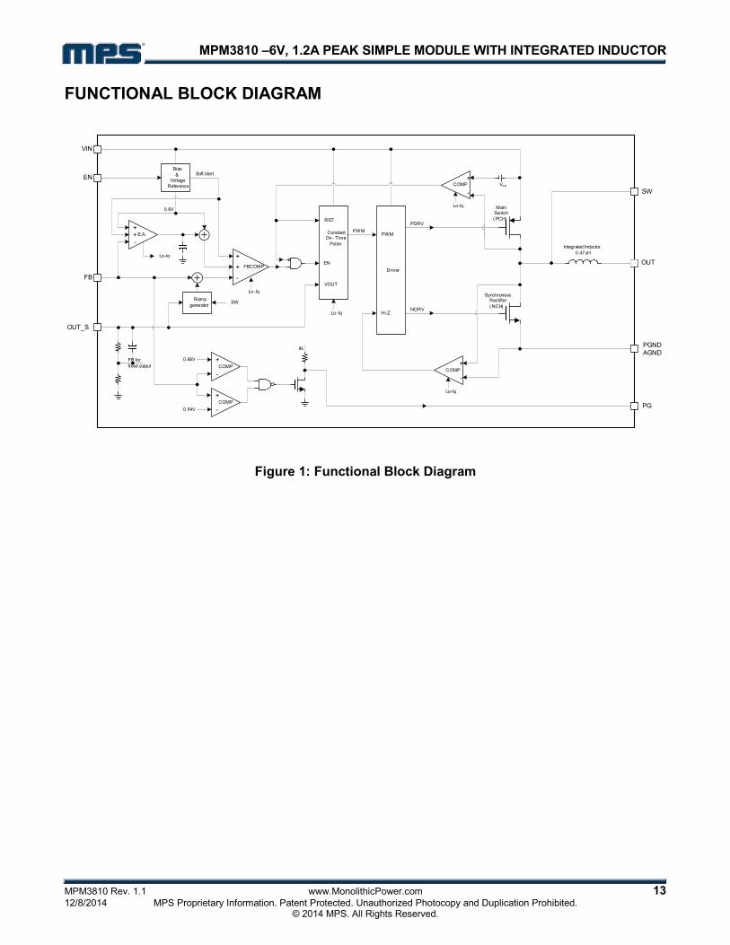
OPERATIONThe DC-DC module has a small surface-mount QFN-12 (2.5mmx3.0mmx0.9mm) package. The module’s integrated inductor simplifies the schematic and layout design. Only FB resistors and input and output capacitors are needed to complete the design. MPM3810 uses constant on-time control (COT) with input voltage feed forward to stabilize the switching frequency over a full-input range. At light load, MPM3810 employs a proprietary control of the low-side switch and inductor current to improve efficiency.
Constant On-Time Control (COT) Compared to a fixed-frequency PWM control, constant on-time control (COT) offers the advantage of a simpler control loop and faster transient response. Using input voltage feed forward, the MPM3810 maintains a nearly constant switching frequency across the input and output voltage range. The on-time of the switching pulse is estimated as follows:
OUTON
IN
VT 0.28usV
= ⋅
To prevent inductor current run away during load transition, MPM3810 fixes the minimum off time to 60ns. However, this minimum off-time limit does not affect operation in a steady state.
Light-Load Operation In a light-load condition, MPM3810 uses a proprietary control scheme to save power and improve efficiency. The MP3810 turns off the low-side switch when the inductor current begins to reverse. Then MP3810 works in discontinuous conduction mode (DCM) operation.
A zero current cross circuit detects if the inductor current begins to reverse. Considering the internal circuit propagation time, the typical delay time is 30ns. This means the inductor current continues to fall after the ZCD is triggered. If the inductor current falling slew rate is fast (Vo voltage is high or close to Vin), the low-side MOSFET turns off (this means the inductor current may be negative). This does not allow the MPM3810 to enter DCM. If DCM is required, the off-time of the low-side MOSFET in continuous conduction mode (CCM) should be longer than 60ns. For example, if Vin is 3.6V and Vo is 3.3V,
the off-time in CCM is 24ns. It is difficult to enter DCM at light load.
Enable (EN) If the input voltage is greater than the under-voltage lockout threshold (UVLO), typically 2.3V, MPM3810 is enabled by pulling EN above 1.2V. Leaving EN to float or be pulled down to ground disables MPM3810. There is an internal 1MΩ resistor from EN to ground.
Soft-Start (SS) MPM3810 has a built-in soft-start that ramps up the output voltage in a controlled slew rate. This avoids overshoot at startup. The soft-start time is about 1.5ms typically.
Power GOOD Indictor (PGOOD) MPM3810 has an open drain with a 550kΩ pull-up resistor pin for the power good indicator (PGOOD). When FB is within +/-10% of regulation voltage (i.e. 0.6V), PGOOD is pulled up to IN by the internal resistor. If FB voltage is out of the +/-10% window, PGOOD is pulled down to ground by an internal MOSFET. The MOSFET has a maximum Rdson of less than 400Ω.
Current Limit MPM3810 has a typical 2.1A current limit for the high-side switch. When the high-side switch reaches the current limit, MPM3810 hits the hiccup threshold until the current decreases. This prevents the inductor current from continuing to build, which results in damage to the components.
Short Circuit and Recovery MPM3810 enters short-circuit protection (SCP) mode when the current limit is reached; then it tries to recover from the short circuit with hiccup mode. In SCP, MPM3810 disables the output power stage, discharges the soft-start cap and then automatically tries to soft-start again. If the short circuit remains after the soft-start ends, MPM3810 repeats the cycle until the short circuit disappears, and the output rises back to the regulation level.
MPM3810 –6V, 1.2A PEAK SIMPLE MODULE WITH INTEGRATED INDUCTOR
APPLICATION INFORMATION COMPONENT SELECTION Setting the Output Voltage The external resistor divider is used to set the output voltage (see Typical Application on page 16). The feedback resistor R1 cannot be too large or too small considering the trade-off for stability and dynamics. Choose R1 between 40kΩ to 80kΩ. R2 is given by:
out
R1R2 V 10.6
=−
The feedback circuit is shown in Figure 2.
R1
R2
OUT
FB
MPM3810
Figure 2: Feedback Network
Table 1 lists the recommended resistor values for common output voltages.
Table 1: Resistor Values for Common Output Voltages
Selecting the Input Capacitor The input current to the step-down converter is discontinuous, therefore a capacitor is required to supply the AC current while maintaining the DC input voltage. For optimal performance, use low ESR capacitors. Ceramic capacitors with X5R or X7R dielectrics are highly recommended due to their low ESR and small temperature coefficients. For most applications, a 10µF capacitor is sufficient.
For higher output voltage, a 22µF may be needed to enhance system stability.
Since the input capacitor absorbs the input switching current, it requires an adequate ripple-current rating. The RMS current in the input capacitor can be estimated by:
OUT OUTC1 LOAD
IN IN
V VI I 1V V⎛ ⎞⎜ ⎟×⎜ ⎟⎜ ⎟⎝ ⎠
= × −
The worst case condition occurs at VIN = 2VOUT, where:
LOADC1
II2
=
For simplification, choose the input capacitor that has a RMS current rating greater than half of the maximum load current.
The input capacitor can be electrolytic, tantalum or ceramic. When using electrolytic or tantalum capacitors, a small, high quality ceramic capacitor (i.e. 0.1μF), should be placed as close to the IC as possible. When using ceramic capacitors, check that they have enough capacitance to provide sufficient charge to prevent an excessive voltage ripple at input. The input-voltage ripple caused by capacitance is estimated by:
LOAD OUT OUTIN
INS IN
I V VV 1f C1 V V
⎛ ⎞Δ = × × −⎜ ⎟× ⎝ ⎠
Selecting the Output Capacitor The output capacitor (COUT) is required to maintain the DC output voltage. Ceramic capacitors are recommended. Low ESR capacitors are preferred to keep the output-voltage ripple low. The output voltage ripple is estimated by:
OUT OUTOUT ESR
S 1 IN S
V V 1V 1 Rf L V 8 f C2
⎛ ⎞⎛ ⎞Δ = × − × +⎜ ⎟⎜ ⎟× × ×⎝ ⎠ ⎝ ⎠
Where L1 is the inductor value, and RESR is the equivalent series resistance (ESR) value of the output capacitor (L1 is 0.47µH).
When using ceramic capacitors, the impedance at the switching frequency is dominated by the capacitance. The output-voltage ripple is mainly
MPM3810 –6V, 1.2A PEAK SIMPLE MODULE WITH INTEGRATED INDUCTOR
caused by the capacitance. For simplification, the output-voltage ripple is estimated by:
OUT OUTOUT 2
S 1 IN
V VΔV 18 f L C2 V
⎛ ⎞= × −⎜ ⎟× × × ⎝ ⎠
When using tantalum or electrolytic capacitors, the ESR dominates the impedance at the switching frequency. For simplification, the output ripple can be approximated by:
OUT OUTOUT ESR
INS 1
V VΔV 1 Rf L V
⎛ ⎞= × − ×⎜ ⎟× ⎝ ⎠
The characteristics of the output capacitor affect the stability of the regulation system.
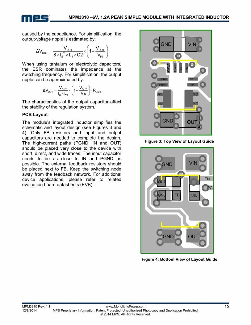
PCB Layout The module’s integrated inductor simplifies the schematic and layout design (see Figures 3 and 4). Only FB resistors and input and output capacitors are needed to complete the design. The high-current paths (PGND, IN and OUT) should be placed very close to the device with short, direct, and wide traces. The input capacitor needs to be as close to IN and PGND as possible. The external feedback resistors should be placed next to FB. Keep the switching node away from the feedback network. For additional device applications, please refer to related evaluation board datasheets (EVB).
GNDGND
PGND
PGND
NC
NC
N/C
N/C
OUT
OUT
VIN
PG
GND OUT
VINGND
Figure 3: Top View of Layout Guide
GND VIN
FB
OUT
GND OUT
EN
PG
VINGND
Figure 4: Bottom View of Layout Guide
MPM3810 –6V, 1.2A PEAK SIMPLE MODULE WITH INTEGRATED INDUCTOR