2 FEATURES .................................................................................................................................................. 6
2.1 GYROSCOPE FEATURES ....................................................................................................................... 6
2.2 ACCELEROMETER FEATURES ............................................................................................................... 6
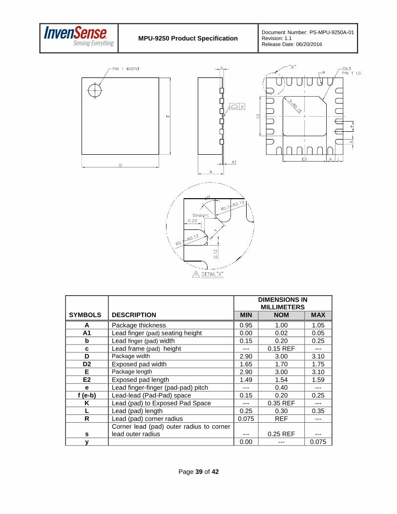
1.2 Purpose and Scope This document provides a description, specifications, and design related information on the MPU-9250 MotionTracking device. The device is housed in a small 3x3x1mm QFN package.
Specifications are subject to change without notice. Final specifications will be updated based upon characterization of production silicon. For references to register map and descriptions of individual registers, please refer to the MPU-9250 Register Map and Register Descriptions document.
1.3 Product Overview MPU-9250 is a multi-chip module (MCM) consisting of two dies integrated into a single QFN package. One die houses the 3-Axis gyroscope and the 3-Axis accelerometer. The other die houses the AK8963 3-Axis magnetometer from Asahi Kasei Microdevices Corporation. Hence, the MPU-9250 is a 9-axis MotionTracking device that combines a 3-axis gyroscope, 3-axis accelerometer, 3-axis magnetometer and a Digital Motion Processor™ (DMP) all in a small 3x3x1mm package available as a pin-compatible upgrade from the MPU-6515. With its dedicated I2C sensor bus, the MPU-9250 directly provides complete 9-axis MotionFusion™ output. The MPU-9250 MotionTracking device, with its 9-axis integration, on-chip MotionFusion™, and run-time calibration firmware, enables manufacturers to eliminate the costly and complex selection, qualification, and system level integration of discrete devices, guaranteeing optimal motion performance for consumers. MPU-9250 is also designed to interface with multiple non-inertial digital sensors, such as pressure sensors, on its auxiliary I2C port.
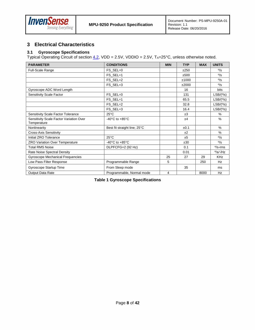
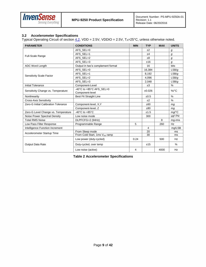
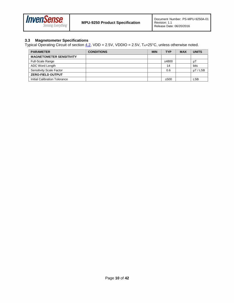
MPU-9250 features three 16-bit analog-to-digital converters (ADCs) for digitizing the gyroscope outputs, three 16-bit ADCs for digitizing the accelerometer outputs, and three 16-bit ADCs for digitizing the magnetometer outputs. For precision tracking of both fast and slow motions, the parts feature a user-programmable gyroscope full-scale range of ±250, ±500, ±1000, and ±2000°/sec (dps), a user-programmable accelerometer full-scale range of ±2g, ±4g, ±8g, and ±16g, and a magnetometer full-scale range of ±4800µT.
Other industry-leading features include programmable digital filters, a precision clock with 1% drift from -40°C to 85°C, an embedded temperature sensor, and programmable interrupts. The device features I2C and SPI serial interfaces, a VDD operating range of 2.4V to 3.6V, and a separate digital IO supply, VDDIO from 1.71V to VDD.
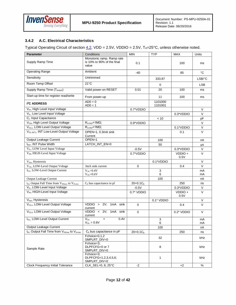
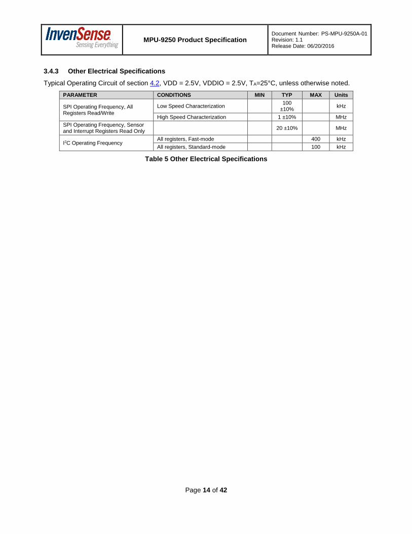
Communication with all registers of the device is performed using either I2C at 400kHz or SPI at 1MHz. For applications requiring faster communications, the sensor and interrupt registers may be read using SPI at 20MHz.
By leveraging its patented and volume-proven CMOS-MEMS fabrication platform, which integrates MEMS wafers with companion CMOS electronics through wafer-level bonding, InvenSense has driven the package size down to a footprint and thickness of 3x3x1mm, to provide a very small yet high performance low cost package. The device provides high robustness by supporting 10,000g shock reliability.
1.4 Applications
Location based services, points of interest, and dead reckoning
Handset and portable gaming
Motion-based game controllers
3D remote controls for Internet connected DTVs and set top boxes, 3D mice
2.1 Gyroscope Features The triple-axis MEMS gyroscope in the MPU-9250 includes a wide range of features:
Digital-output X-, Y-, and Z-Axis angular rate sensors (gyroscopes) with a user-programmable full-scale range of ±250, ±500, ±1000, and ±2000°/sec and integrated 16-bit ADCs
Digitally-programmable low-pass filter
Gyroscope operating current: 3.2mA
Sleep mode current: 8µA
Factory calibrated sensitivity scale factor
Self-test
2.2 Accelerometer Features The triple-axis MEMS accelerometer in MPU-9250 includes a wide range of features:
Digital-output triple-axis accelerometer with a programmable full scale range of ±2g, ±4g, ±8g and ±16g and integrated 16-bit ADCs
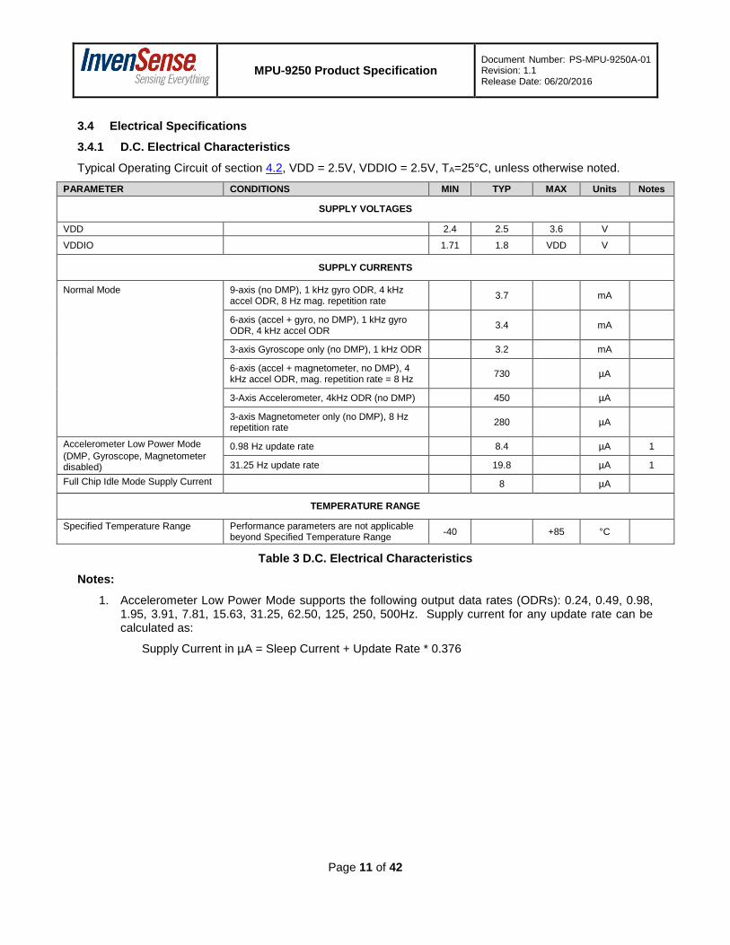
Accelerometer normal operating current: 450µA
Low power accelerometer mode current: 8.4µA at 0.98Hz, 19.8µA at 31.25Hz
Sleep mode current: 8µA
User-programmable interrupts
Wake-on-motion interrupt for low power operation of applications processor
Self-test
2.3 Magnetometer Features The triple-axis MEMS magnetometer in MPU-9250 includes a wide range of features:
3-axis silicon monolithic Hall-effect magnetic sensor with magnetic concentrator
Wide dynamic measurement range and high resolution with lower current consumption.
Output data resolution of 14 bit (0.6µT/LSB)
Full scale measurement range is ±4800µT
Magnetometer normal operating current: 280µA at 8Hz repetition rate
Self-test function with internal magnetic source to confirm magnetic sensor operation on end products
2.4 Additional Features The MPU-9250 includes the following additional features:
Auxiliary master I2C bus for reading data from external sensors (e.g. pressure sensor)
3.5mA operating current when all 9 motion sensing axes and the DMP are enabled
VDD supply voltage range of 2.4 – 3.6V
VDDIO reference voltage for auxiliary I2C devices
Smallest and thinnest QFN package for portable devices: 3x3x1mm
Minimal cross-axis sensitivity between the accelerometer, gyroscope and magnetometer axes
512 byte FIFO buffer enables the applications processor to read the data in bursts
Digital-output temperature sensor
User-programmable digital filters for gyroscope, accelerometer, and temp sensor
10,000 g shock tolerant
400kHz Fast Mode I2C for communicating with all registers
1MHz SPI serial interface for communicating with all registers
20MHz SPI serial interface for reading sensor and interrupt registers
MEMS structure hermetically sealed and bonded at wafer level
RoHS and Green compliant
2.5 MotionProcessing
Internal Digital Motion Processing™ (DMP™) engine supports advanced MotionProcessing and low power functions such as gesture recognition using programmable interrupts
Low-power pedometer functionality allows the host processor to sleep while the DMP maintains the step count.
3-axis Magnetometer only (no DMP), 8 Hz repetition rate
280 µA
Accelerometer Low Power Mode
(DMP, Gyroscope, Magnetometer disabled)
0.98 Hz update rate 8.4 µA 1
31.25 Hz update rate 19.8 µA 1
Full Chip Idle Mode Supply Current 8 µA
TEMPERATURE RANGE
Specified Temperature Range Performance parameters are not applicable beyond Specified Temperature Range
-40 +85 °C
Table 3 D.C. Electrical Characteristics
Notes:
1. Accelerometer Low Power Mode supports the following output data rates (ODRs): 0.24, 0.49, 0.98, 1.95, 3.91, 7.81, 15.63, 31.25, 62.50, 125, 250, 500Hz. Supply current for any update rate can be calculated as:
Supply Current in µA = Sleep Current + Update Rate * 0.376
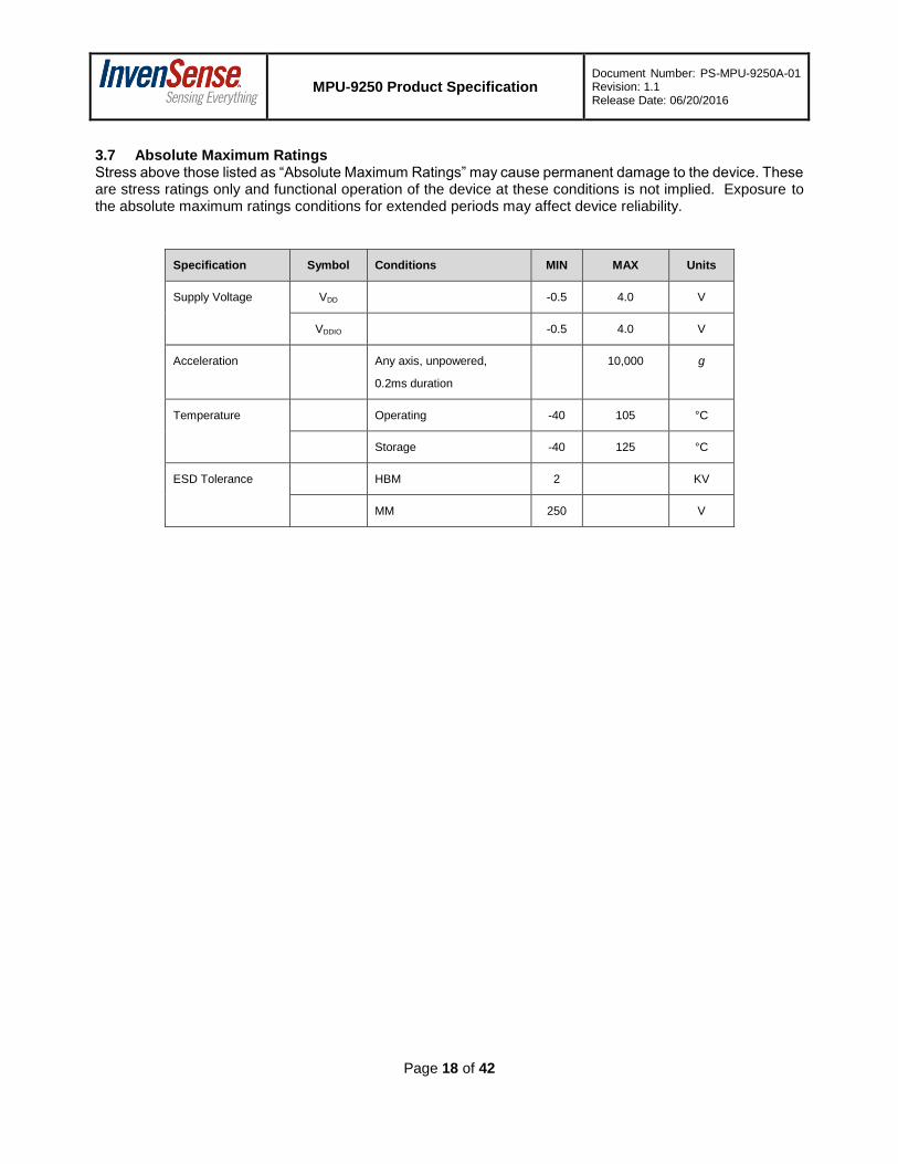
3.7 Absolute Maximum Ratings Stress above those listed as “Absolute Maximum Ratings” may cause permanent damage to the device. These are stress ratings only and functional operation of the device at these conditions is not implied. Exposure to the absolute maximum ratings conditions for extended periods may affect device reliability.
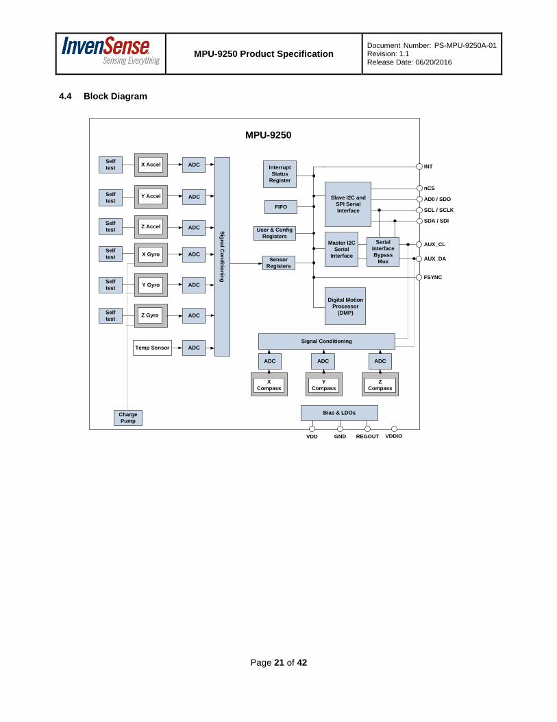
4.5 Overview The MPU-9250 is comprised of the following key blocks and functions:
Three-axis MEMS rate gyroscope sensor with 16-bit ADCs and signal conditioning
Three-axis MEMS accelerometer sensor with 16-bit ADCs and signal conditioning
Three-axis MEMS magnetometer sensor with 16-bit ADCs and signal conditioning
Digital Motion Processor (DMP) engine
Primary I2C and SPI serial communications interfaces
Auxiliary I2C serial interface for 3rd party sensors
Clocking
Sensor Data Registers
FIFO
Interrupts
Digital-Output Temperature Sensor
Gyroscope, Accelerometer and Magnetometer Self-test
Bias and LDO
Charge Pump
4.6 Three-Axis MEMS Gyroscope with 16-bit ADCs and Signal Conditioning
The MPU-9250 consists of three independent vibratory MEMS rate gyroscopes, which detect rotation about the X-, Y-, and Z- Axes. When the gyros are rotated about any of the sense axes, the Coriolis Effect causes a vibration that is detected by a capacitive pickoff. The resulting signal is amplified, demodulated, and filtered to produce a voltage that is proportional to the angular rate. This voltage is digitized using individual on-chip 16-bit Analog-to-Digital Converters (ADCs) to sample each axis. The full-scale range of the gyro sensors may be digitally programmed to ±250, ±500, ±1000, or ±2000 degrees per second (dps). The ADC sample rate is programmable from 8,000 samples per second, down to 3.9 samples per second, and user-selectable low-pass filters enable a wide range of cut-off frequencies.
4.7 Three-Axis MEMS Accelerometer with 16-bit ADCs and Signal Conditioning
The MPU-9250’s 3-Axis accelerometer uses separate proof masses for each axis. Acceleration along a particular axis induces displacement on the corresponding proof mass, and capacitive sensors detect the displacement differentially. The MPU-9250’s architecture reduces the accelerometers’ susceptibility to fabrication variations as well as to thermal drift. When the device is placed on a flat surface, it will measure 0g on the X- and Y-axes and +1g on the Z-axis. The accelerometers’ scale factor is calibrated at the factory and is nominally independent of supply voltage. Each sensor has a dedicated sigma-delta ADC for providing digital outputs. The full scale range of the digital output can be adjusted to ±2g, ±4g, ±8g, or ±16g.
4.8 Three-Axis MEMS Magnetometer with 16-bit ADCs and Signal Conditioning
The 3-axis magnetometer uses highly sensitive Hall sensor technology. The magnetometer portion of the IC incorporates magnetic sensors for detecting terrestrial magnetism in the X-, Y-, and Z- Axes, a sensor driving circuit, a signal amplifier chain, and an arithmetic circuit for processing the signal from each sensor. Each ADC has a 16-bit resolution and a full scale range of ±4800 µT.
4.9 Digital Motion Processor
The embedded Digital Motion Processor (DMP) is located within the MPU-9250 and offloads computation of motion processing algorithms from the host processor. The DMP acquires data from accelerometers,
gyroscopes, magnetometers and additional 3rd party sensors, and processes the data. The resulting data can be read from the DMP’s registers, or can be buffered in a FIFO. The DMP has access to one of the MPU’s external pins, which can be used for generating interrupts. This pin (pin 12) should be connected to a pin on the host processor that can wake the host from suspend mode.
The purpose of the DMP is to offload both timing requirements and processing power from the host processor. Typically, motion processing algorithms should be run at a high rate, often around 200Hz, in order to provide accurate results with low latency. This is required even if the application updates at a much lower rate; for example, a low power user interface may update as slowly as 5Hz, but the motion processing should still run at 200Hz. The DMP can be used as a tool in order to minimize power, simplify timing, simplify the software architecture, and save valuable MIPS on the host processor for use in the application.
4.10 Primary I2C and SPI Serial Communications Interfaces The MPU-9250 communicates to a system processor using either a SPI or an I2C serial interface. The MPU-9250 always acts as a slave when communicating to the system processor. The LSB of the of the I2C slave address is set by pin 9 (AD0).
4.11 Auxiliary I2C Serial Interface The MPU-9250 has an auxiliary I2C bus for communicating to off-chip sensors. This bus has two operating modes:
I2C Master Mode: The MPU-9250 acts as a master to any external sensors connected to the auxiliary I2C bus
Pass-Through Mode: The MPU-9250 directly connects the primary and auxiliary I2C buses together, allowing the system processor to directly communicate with any external sensors.
Note: AUX_DA and AUX_CL should be left unconnected if the Auxiliary I2C mode is not used.
Auxiliary I2C Bus Modes of Operation:
I2C Master Mode: Allows the MPU-9250 to directly access the data registers of external digital sensors, such as a magnetometer. In this mode, the MPU-9250 directly obtains data from auxiliary sensors without intervention from the system applications processor.
For example, In I2C Master mode, the MPU-9250 can be configured to perform burst reads, returning the following data from a magnetometer:
X magnetometer data (2 bytes) Y magnetometer data (2 bytes) Z magnetometer data (2 bytes)
The I2C Master can be configured to read up to 24 bytes from up to 4 auxiliary sensors. A fifth sensor can be configured to work single byte read/write mode.
Pass-Through Mode: Allows an external system processor to act as master and directly communicate to the external sensors connected to the auxiliary I2C bus pins (AUX_DA and AUX_CL). In this mode, the auxiliary I2C bus control logic (3rd party sensor interface block) of the MPU-9250 is disabled, and the auxiliary I2C pins AUX_DA and AUX_CL are connected to the main I2C bus through analog switches internally.
Pass-Through mode is useful for configuring the external sensors, or for keeping the MPU-9250 in a low-power mode when only the external sensors are used. In this mode, the system processor can still access MPU-9250 data through the I2C interface. Pass-Through mode is also used to access the AK8963 magnetometer directly from the host. In this configuration the slave address for the AK8963 is 0X0C or 12 decimal.
Auxiliary I2C Bus IO Logic Levels
For MPU-9250, the logic level of the auxiliary I2C bus is VDDIO. For further information regarding the MPU-9250 logic levels, please refer to Section 10.2.
4.12 Self-Test Please refer to the register map document for more details on self-test.
Self-test allows for the testing of the mechanical and electrical portions of the sensors. The self-test for each measurement axis can be activated by means of the gyroscope and accelerometer self-test registers (registers 13 to 16).
When the self-test is activated, the electronics cause the sensors to be actuated and produce an output signal. The output signal is used to observe the self-test response.
The self-test response is defined as follows:
Self-test response = Sensor output with self-test enabled – Sensor output without self-test enabled
When the value of the self-test response is within the appropriate limits, the part has passed self-test. When the self-test response exceeds the appropriate values, the part is deemed to have failed self-test. It is recommended to use InvenSense MotionApps software for executing self-test. Further details, including the self-test limits are included in the MPU-9250 Self-Test applications note available from InvenSense.
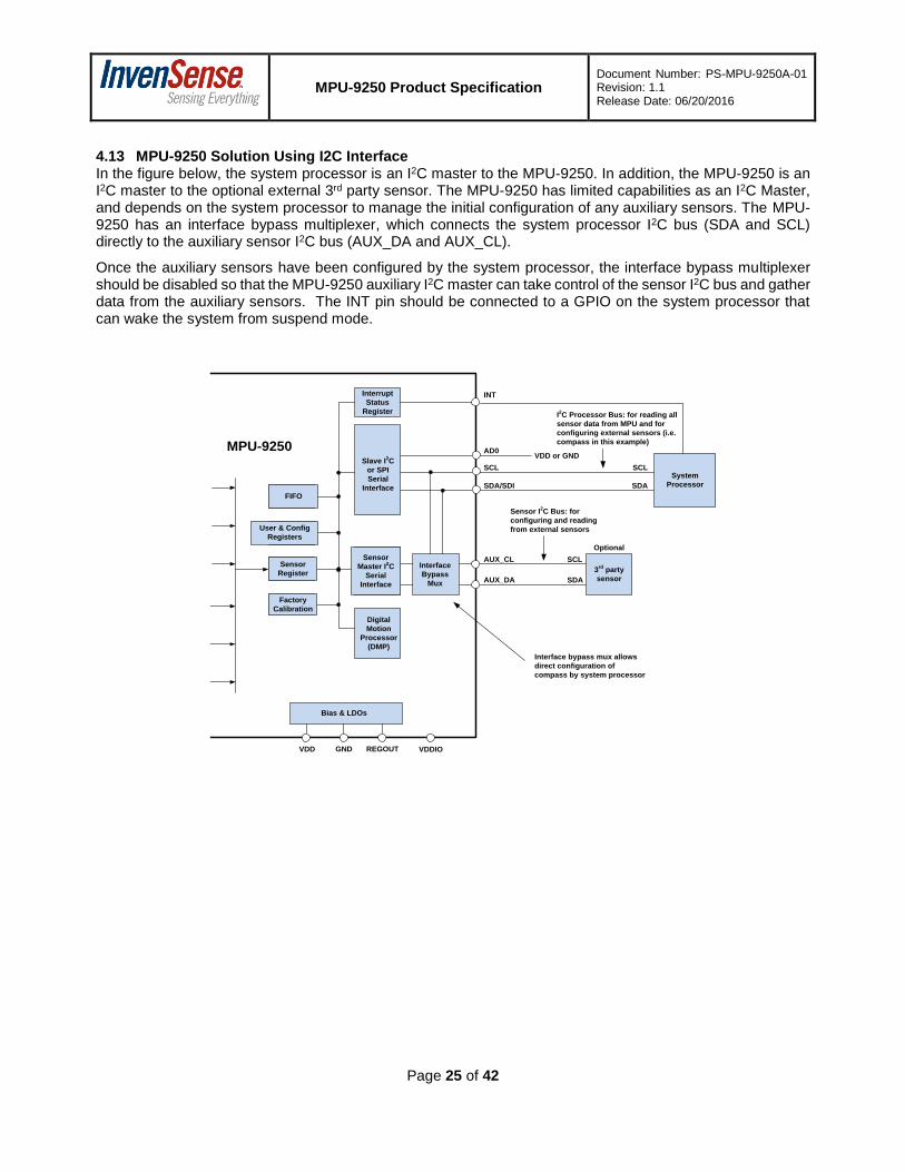
4.13 MPU-9250 Solution Using I2C Interface In the figure below, the system processor is an I2C master to the MPU-9250. In addition, the MPU-9250 is an I2C master to the optional external 3rd party sensor. The MPU-9250 has limited capabilities as an I2C Master, and depends on the system processor to manage the initial configuration of any auxiliary sensors. The MPU-9250 has an interface bypass multiplexer, which connects the system processor I2C bus (SDA and SCL) directly to the auxiliary sensor I2C bus (AUX_DA and AUX_CL).
Once the auxiliary sensors have been configured by the system processor, the interface bypass multiplexer should be disabled so that the MPU-9250 auxiliary I2C master can take control of the sensor I2C bus and gather data from the auxiliary sensors. The INT pin should be connected to a GPIO on the system processor that can wake the system from suspend mode.
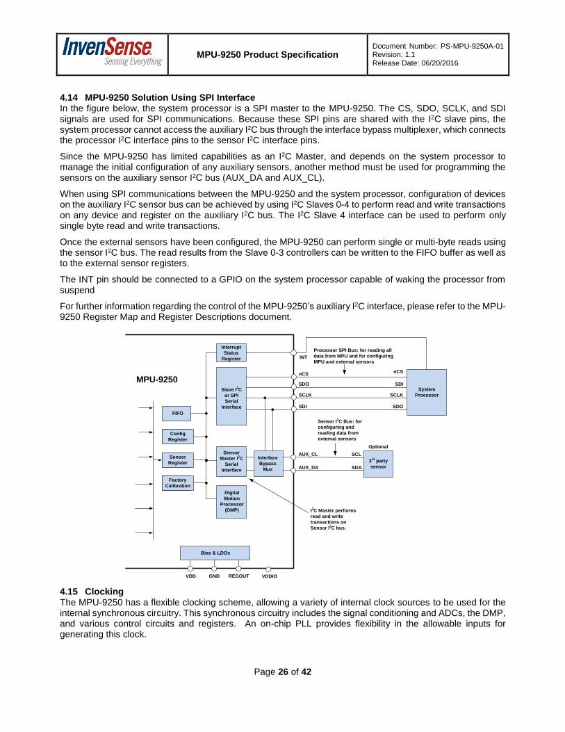
4.14 MPU-9250 Solution Using SPI Interface In the figure below, the system processor is a SPI master to the MPU-9250. The CS, SDO, SCLK, and SDI signals are used for SPI communications. Because these SPI pins are shared with the I2C slave pins, the system processor cannot access the auxiliary I2C bus through the interface bypass multiplexer, which connects the processor I2C interface pins to the sensor I2C interface pins.
Since the MPU-9250 has limited capabilities as an I2C Master, and depends on the system processor to manage the initial configuration of any auxiliary sensors, another method must be used for programming the sensors on the auxiliary sensor I2C bus (AUX_DA and AUX_CL).
When using SPI communications between the MPU-9250 and the system processor, configuration of devices on the auxiliary I2C sensor bus can be achieved by using I2C Slaves 0-4 to perform read and write transactions on any device and register on the auxiliary I2C bus. The I2C Slave 4 interface can be used to perform only single byte read and write transactions.
Once the external sensors have been configured, the MPU-9250 can perform single or multi-byte reads using the sensor I2C bus. The read results from the Slave 0-3 controllers can be written to the FIFO buffer as well as to the external sensor registers.
The INT pin should be connected to a GPIO on the system processor capable of waking the processor from suspend
For further information regarding the control of the MPU-9250’s auxiliary I2C interface, please refer to the MPU-9250 Register Map and Register Descriptions document.
MPU-9250SDO
SCLK
SDI
Digital
Motion
Processor
(DMP)
Sensor
Master I2C
Serial
Interface
Interrupt
Status
Register INT
FIFO
Config
Register
Sensor
Register
Factory
Calibration
nCS
Slave I2C
or SPI
Serial
Interface
System
Processor
Interface
Bypass
Mux
SDI
SCLK
SDO
nCS
Processor SPI Bus: for reading all
data from MPU and for configuring
MPU and external sensors
AUX_CL
AUX_DA
3rd
party
sensor
SCL
SDA
Optional
I2C Master performs
read and write
transactions on
Sensor I2C bus.
Sensor I2C Bus: for
configuring and
reading data from
external sensors
VDD
Bias & LDOs
GND REGOUT VDDIO
4.15 Clocking The MPU-9250 has a flexible clocking scheme, allowing a variety of internal clock sources to be used for the internal synchronous circuitry. This synchronous circuitry includes the signal conditioning and ADCs, the DMP, and various control circuits and registers. An on-chip PLL provides flexibility in the allowable inputs for generating this clock.
Allowable internal sources for generating the internal clock are:
An internal relaxation oscillator
Any of the X, Y, or Z gyros (MEMS oscillators with a variation of ±1% over temperature)
Selection of the source for generating the internal synchronous clock depends on the requirements for power consumption and clock accuracy. These requirements will most likely vary by mode of operation. For example, in one mode, where the biggest concern is power consumption, the user may wish to operate the Digital Motion Processor of the MPU-9250 to process accelerometer data, while keeping the gyros off. In this case, the internal relaxation oscillator is a good clock choice. However, in another mode, where the gyros are active, selecting the gyros as the clock source provides for a more accurate clock source.
Clock accuracy is important, since timing errors directly affect the distance and angle calculations performed by the Digital Motion Processor (and by extension, by any processor).
There are also start-up conditions to consider. When the MPU-9250 first starts up, the device uses its internal clock until programmed to operate from another source. This allows the user, for example, to wait for the MEMS oscillators to stabilize before they are selected as the clock source.
4.16 Sensor Data Registers The sensor data registers contain the latest gyroscope, accelerometer, magnetometer, auxiliary sensor, and temperature measurement data. They are read-only registers, and are accessed via the serial interface. Data from these registers may be read anytime.
4.17 FIFO The MPU-9250 contains a 512-byte FIFO register that is accessible via the Serial Interface. The FIFO configuration register determines which data is written into the FIFO. Possible choices include gyro data, accelerometer data, temperature readings, auxiliary sensor readings, and FSYNC input. A FIFO counter keeps track of how many bytes of valid data are contained in the FIFO. The FIFO register supports burst reads. The interrupt function may be used to determine when new data is available.
For further information regarding the FIFO, please refer to the MPU-9250 Register Map and Register Descriptions document.
4.18 Interrupts Interrupt functionality is configured via the Interrupt Configuration register. Items that are configurable include the INT pin configuration, the interrupt latching and clearing method, and triggers for the interrupt. Items that can trigger an interrupt are (1) Clock generator locked to new reference oscillator (used when switching clock sources); (2) new data is available to be read (from the FIFO and Data registers); (3) accelerometer event interrupts; and (4) the MPU-9250 did not receive an acknowledge from an auxiliary sensor on the secondary I2C bus. The interrupt status can be read from the Interrupt Status register.
The INT pin should be connected to a pin on the host processor capable of waking that processor from suspend.
For further information regarding interrupts, please refer to the MPU-9250 Register Map and Register Descriptions document.
4.19 Digital-Output Temperature Sensor An on-chip temperature sensor and ADC are used to measure the MPU-9250 die temperature. The readings from the ADC can be read from the FIFO or the Sensor Data registers.
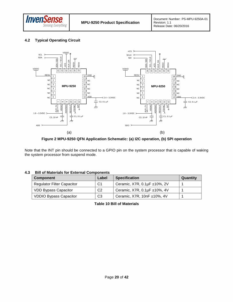
4.20 Bias and LDO The bias and LDO section generates the internal supply and the reference voltages and currents required by the MPU-9250. Its two inputs are an unregulated VDD and a VDDIO logic reference supply voltage. The LDO output is bypassed by a capacitor at REGOUT. For further details on the capacitor, please refer to the Bill of Materials for External Components.
4.21 Charge Pump An on-chip charge pump generates the high voltage required for the MEMS oscillators.
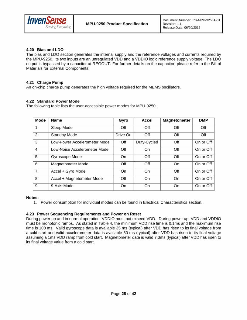
4.22 Standard Power Mode The following table lists the user-accessible power modes for MPU-9250.
Mode Name Gyro Accel Magnetometer DMP
1 Sleep Mode Off Off Off Off
2 Standby Mode Drive On Off Off Off
3 Low-Power Accelerometer Mode Off Duty-Cycled Off On or Off
4 Low-Noise Accelerometer Mode Off On Off On or Off
5 Gyroscope Mode On Off Off On or Off
6 Magnetometer Mode Off Off On On or Off
7 Accel + Gyro Mode On On Off On or Off
8 Accel + Magnetometer Mode Off On On On or Off
9 9-Axis Mode On On On On or Off
Notes:
1. Power consumption for individual modes can be found in Electrical Characteristics section.
4.23 Power Sequencing Requirements and Power on Reset During power up and in normal operation, VDDIO must not exceed VDD. During power up, VDD and VDDIO must be monotonic ramps. As stated in Table 4, the minimum VDD rise time is 0.1ms and the maximum rise time is 100 ms. Valid gyroscope data is available 35 ms (typical) after VDD has risen to its final voltage from a cold start and valid accelerometer data is available 30 ms (typical) after VDD has risen to its final voltage assuming a 1ms VDD ramp from cold start. Magnetometer data is valid 7.3ms (typical) after VDD has risen to its final voltage value from a cold start.
The MPU-9250 has a programmable interrupt system which can generate an interrupt signal on the INT pin. Status flags indicate the source of an interrupt. Interrupt sources may be enabled and disabled individually.
Table of Interrupt Sources
Interrupt Name Module
Motion Detection Motion
FIFO Overflow FIFO
Data Ready Sensor Registers
I2C Master errors: Lost Arbitration, NACKs I2C Master
I2C Slave 4 I2C Master
For information regarding the interrupt enable/disable registers and flag registers, please refer to the MPU-9250 Register Map and Register Descriptions document. Some interrupt sources are explained below.
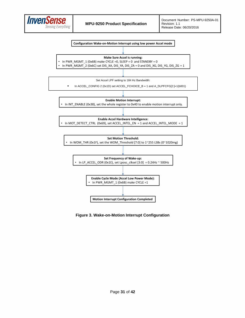
6.1 Wake-on-Motion Interrupt The MPU-9250 provides motion detection capability. A qualifying motion sample is one where the high passed sample from any axis has an absolute value exceeding a user-programmable threshold. The following flowchart explains how to configure the Wake-on-Motion Interrupt. For further details on individual registers, please refer to the MPU-9250 Registers Map and Registers Description document.
In order to properly enable motion interrupts, the INT pin should be connected to a GPIO on the system processor that is capable of waking up the system processor.
Configuration Wake-on-Motion Interrupt using low power Accel mode
Make Sure Accel is running:• In PWR_MGMT_1 (0x6B) make CYCLE =0, SLEEP = 0 and STANDBY = 0• In PWR_MGMT_2 (0x6C) set DIS_XA, DIS_YA, DIS_ZA = 0 and DIS_XG, DIS_YG, DIS_ZG = 1
Set Accel LPF setting to 184 Hz Bandwidth:• In ACCEL_CONFIG 2 (0x1D) set ACCEL_FCHOICE_B = 0 and A_DLPFCFG[2:0]=1(b001)
Enable Motion Interrupt:• In INT_ENABLE (0x38), set the whole register to 0x40 to enable motion interrupt only.
Enable Accel Hardware Intelligence:• In MOT_DETECT_CTRL (0x69), set ACCEL_INTEL_EN = 1 and ACCEL_INTEL_MODE = 1
Set Motion Threshold:• In WOM_THR (0x1F), set the WOM_Threshold [7:0] to 1~255 LSBs (0~1020mg)
Set Frequency of Wake-up:• In LP_ACCEL_ODR (0x1E), set Lposc_clksel [3:0] = 0.24Hz ~ 500Hz
Enable Cycle Mode (Accel Low Power Mode):• In PWR_MGMT_1 (0x6B) make CYCLE =1
Motion Interrupt Configuration Completed
Set Accel LPF setting to 184 Hz Bandwidth:
In ACCEL_CONFIG 2 (0x1D) set ACCEL_FCHOICE_B = 1 and A_DLPFCFG[2:]=1(b001)
7.1 I2C and SPI Serial Interfaces The internal registers and memory of the MPU-9250 can be accessed using either I2C at 400 kHz or SPI at 1MHz. SPI operates in four-wire mode.
Serial Interface
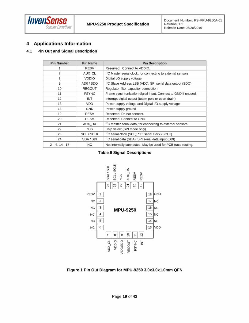
Pin Number Pin Name Pin Description
8 VDDIO Digital I/O supply voltage.
9 AD0 / SDO I2C Slave Address LSB (AD0); SPI serial data output (SDO)
23 SCL / SCLK I2C serial clock (SCL); SPI serial clock (SCLK)
24 SDA / SDI I2C serial data (SDA); SPI serial data input (SDI)
Note:
To prevent switching into I2C mode when using SPI, the I2C interface should be disabled by setting the I2C_IF_DIS configuration bit. Setting this bit should be performed immediately after waiting for the time specified by the “Start-Up Time for Register Read/Write” in Section 6.3.
For further information regarding the I2C_IF_DIS bit, please refer to the MPU-9250 Register Map and Register Descriptions document.
7.2 I2C Interface I2C is a two-wire interface comprised of the signals serial data (SDA) and serial clock (SCL). In general, the lines are open-drain and bi-directional. In a generalized I2C interface implementation, attached devices can be a master or a slave. The master device puts the slave address on the bus, and the slave device with the matching address acknowledges the master.
The MPU-9250 always operates as a slave device when communicating to the system processor, which thus acts as the master. SDA and SCL lines typically need pull-up resistors to VDD. The maximum bus speed is 400 kHz.
The slave address of the MPU-9250 is b110100X which is 7 bits long. The LSB bit of the 7 bit address is determined by the logic level on pin AD0. This allows two MPU-9250s to be connected to the same I2C bus. When used in this configuration, the address of the one of the devices should be b1101000 (pin AD0 is logic low) and the address of the other should be b1101001 (pin AD0 is logic high).
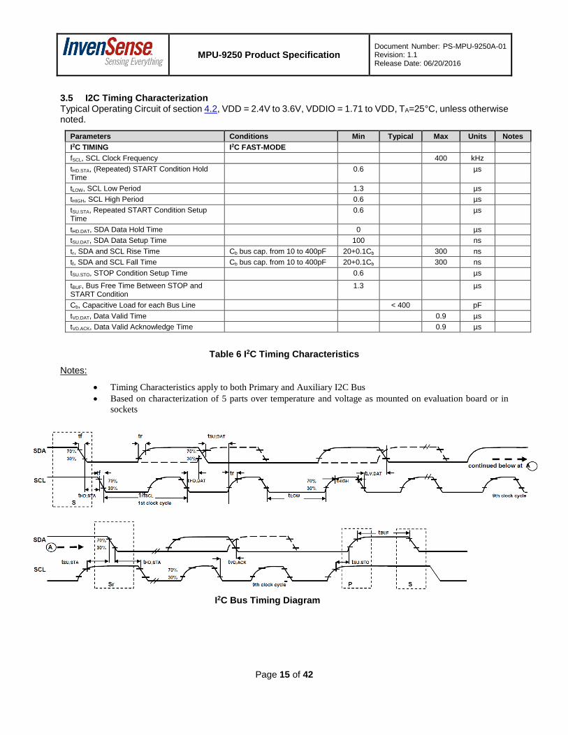
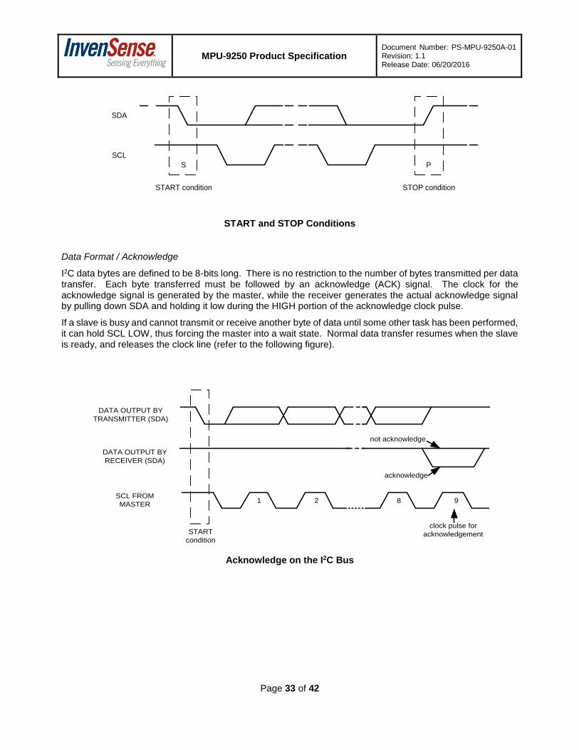
7.3 I2C Communications Protocol START (S) and STOP (P) Conditions
Communication on the I2C bus starts when the master puts the START condition (S) on the bus, which is defined as a HIGH-to-LOW transition of the SDA line while SCL line is HIGH (see figure below). The bus is considered to be busy until the master puts a STOP condition (P) on the bus, which is defined as a LOW to HIGH transition on the SDA line while SCL is HIGH (see figure below).
Additionally, the bus remains busy if a repeated START (Sr) is generated instead of a STOP condition.
I2C data bytes are defined to be 8-bits long. There is no restriction to the number of bytes transmitted per data transfer. Each byte transferred must be followed by an acknowledge (ACK) signal. The clock for the acknowledge signal is generated by the master, while the receiver generates the actual acknowledge signal by pulling down SDA and holding it low during the HIGH portion of the acknowledge clock pulse.
If a slave is busy and cannot transmit or receive another byte of data until some other task has been performed, it can hold SCL LOW, thus forcing the master into a wait state. Normal data transfer resumes when the slave is ready, and releases the clock line (refer to the following figure).
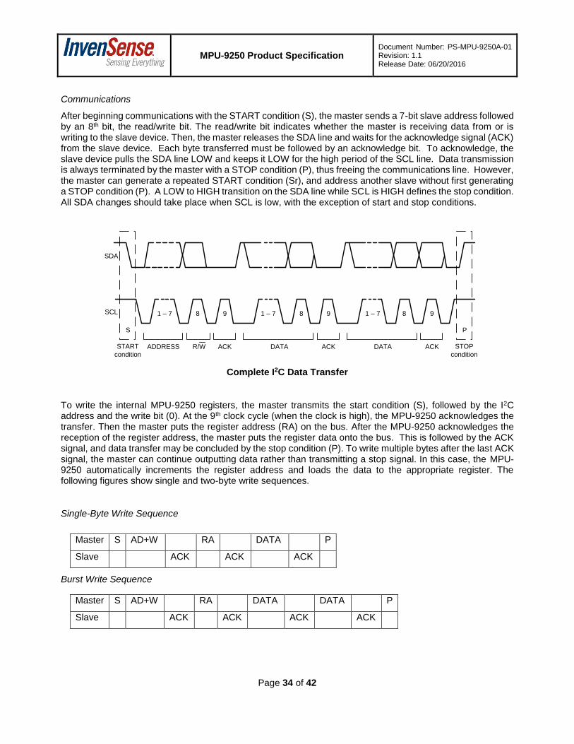
After beginning communications with the START condition (S), the master sends a 7-bit slave address followed by an 8th bit, the read/write bit. The read/write bit indicates whether the master is receiving data from or is writing to the slave device. Then, the master releases the SDA line and waits for the acknowledge signal (ACK) from the slave device. Each byte transferred must be followed by an acknowledge bit. To acknowledge, the slave device pulls the SDA line LOW and keeps it LOW for the high period of the SCL line. Data transmission is always terminated by the master with a STOP condition (P), thus freeing the communications line. However, the master can generate a repeated START condition (Sr), and address another slave without first generating a STOP condition (P). A LOW to HIGH transition on the SDA line while SCL is HIGH defines the stop condition. All SDA changes should take place when SCL is low, with the exception of start and stop conditions.
SDA
START
condition
SCL
ADDRESS R/W ACK DATA ACK DATA ACK STOP
condition
S P
1 – 7 8 9 1 – 7 8 9 1 – 7 8 9
Complete I2C Data Transfer
To write the internal MPU-9250 registers, the master transmits the start condition (S), followed by the I2C address and the write bit (0). At the 9th clock cycle (when the clock is high), the MPU-9250 acknowledges the transfer. Then the master puts the register address (RA) on the bus. After the MPU-9250 acknowledges the reception of the register address, the master puts the register data onto the bus. This is followed by the ACK signal, and data transfer may be concluded by the stop condition (P). To write multiple bytes after the last ACK signal, the master can continue outputting data rather than transmitting a stop signal. In this case, the MPU-9250 automatically increments the register address and loads the data to the appropriate register. The following figures show single and two-byte write sequences.
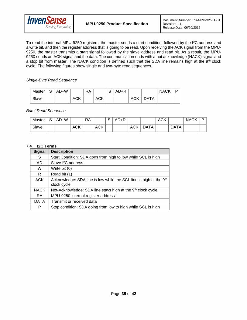
To read the internal MPU-9250 registers, the master sends a start condition, followed by the I2C address and a write bit, and then the register address that is going to be read. Upon receiving the ACK signal from the MPU-9250, the master transmits a start signal followed by the slave address and read bit. As a result, the MPU-9250 sends an ACK signal and the data. The communication ends with a not acknowledge (NACK) signal and a stop bit from master. The NACK condition is defined such that the SDA line remains high at the 9 th clock cycle. The following figures show single and two-byte read sequences.
Single-Byte Read Sequence
Burst Read Sequence
7.4 I2C Terms
Signal Description
S Start Condition: SDA goes from high to low while SCL is high
AD Slave I2C address
W Write bit (0)
R Read bit (1)
ACK Acknowledge: SDA line is low while the SCL line is high at the 9th clock cycle
NACK Not-Acknowledge: SDA line stays high at the 9th clock cycle
RA MPU-9250 internal register address
DATA Transmit or received data
P Stop condition: SDA going from low to high while SCL is high
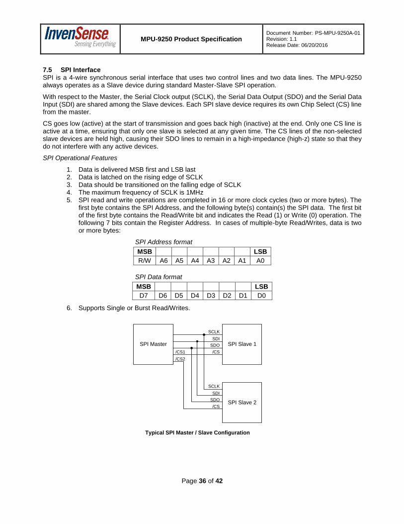
7.5 SPI Interface SPI is a 4-wire synchronous serial interface that uses two control lines and two data lines. The MPU-9250 always operates as a Slave device during standard Master-Slave SPI operation.
With respect to the Master, the Serial Clock output (SCLK), the Serial Data Output (SDO) and the Serial Data Input (SDI) are shared among the Slave devices. Each SPI slave device requires its own Chip Select (CS) line from the master.
CS goes low (active) at the start of transmission and goes back high (inactive) at the end. Only one CS line is active at a time, ensuring that only one slave is selected at any given time. The CS lines of the non-selected slave devices are held high, causing their SDO lines to remain in a high-impedance (high-z) state so that they do not interfere with any active devices.
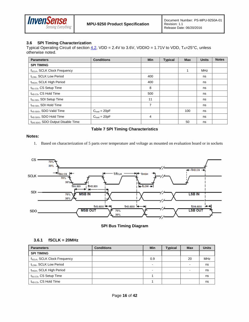
SPI Operational Features
1. Data is delivered MSB first and LSB last 2. Data is latched on the rising edge of SCLK 3. Data should be transitioned on the falling edge of SCLK 4. The maximum frequency of SCLK is 1MHz 5. SPI read and write operations are completed in 16 or more clock cycles (two or more bytes). The
first byte contains the SPI Address, and the following byte(s) contain(s) the SPI data. The first bit of the first byte contains the Read/Write bit and indicates the Read (1) or Write (0) operation. The following 7 bits contain the Register Address. In cases of multiple-byte Read/Writes, data is two or more bytes:
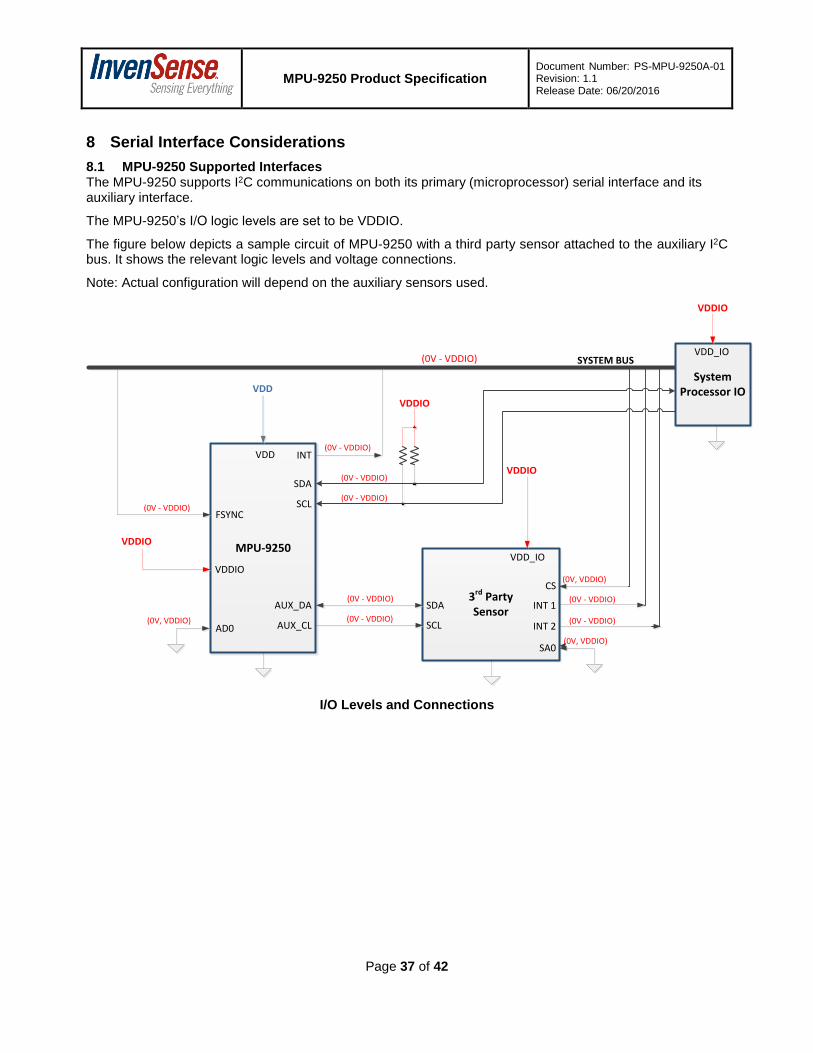
8.1 MPU-9250 Supported Interfaces The MPU-9250 supports I2C communications on both its primary (microprocessor) serial interface and its auxiliary interface.
The MPU-9250’s I/O logic levels are set to be VDDIO.
The figure below depicts a sample circuit of MPU-9250 with a third party sensor attached to the auxiliary I2C bus. It shows the relevant logic levels and voltage connections.
Note: Actual configuration will depend on the auxiliary sensors used.
This section provides general guidelines for assembling InvenSense Micro Electro-Mechanical Systems (MEMS) devices packaged in quad flat no-lead package (QFN) surface mount integrated circuits.
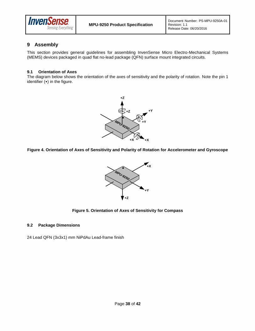
9.1 Orientation of Axes The diagram below shows the orientation of the axes of sensitivity and the polarity of rotation. Note the pin 1 identifier (•) in the figure.
MPU-9250
+Z
+X
+Y
+Z
+Y
+X
Figure 4. Orientation of Axes of Sensitivity and Polarity of Rotation for Accelerometer and Gyroscope
MPU-9250
+Z
+X
+Y
Figure 5. Orientation of Axes of Sensitivity for Compass
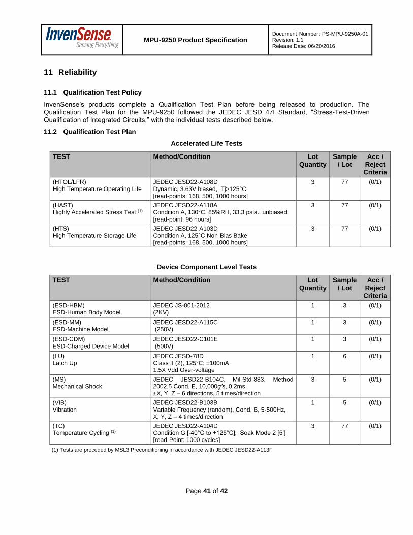
InvenSense’s products complete a Qualification Test Plan before being released to production. The Qualification Test Plan for the MPU-9250 followed the JEDEC JESD 47I Standard, “Stress-Test-Driven Qualification of Integrated Circuits,” with the individual tests described below.
Please refer to “InvenSense MEMS Handling Application Note (AN-IVS-0002A-00)” for the following information:
Manufacturing Recommendations o Assembly Guidelines and Recommendations o PCB Design Guidelines and Recommendations o MEMS Handling Instructions o ESD Considerations o Reflow Specification o Storage Specifications o Package Marking Specification o Tape & Reel Specification o Reel & Pizza Box Label o Packaging o Representative Shipping Carton Label
Compliance o Environmental Compliance o DRC Compliance o Compliance Declaration Disclaimer
This information furnished by InvenSense is believed to be accurate and reliable. However, no responsibility is assumed by InvenSense for its use, or for any infringements of patents or other rights of third parties that may result from its use. Specifications are subject to change without notice. InvenSense reserves the right to make changes to this product, including its circuits and software, in order to improve its design and/or performance, without prior notice. InvenSense makes no warranties, neither expressed nor implied, regarding the information and specifications contained in this document. InvenSense assumes no responsibility for any claims or damages arising from information contained in this document, or from the use of products and services detailed therein. This includes, but is not limited to, claims or damages based on the infringement of patents, copyrights, mask work and/or other intellectual property rights.
Certain intellectual property owned by InvenSense and described in this document is patent protected. No license is granted by implication or otherwise under any patent or patent rights of InvenSense. This publication supersedes and replaces all information previously supplied. Trademarks that are registered trademarks are the property of their respective companies. InvenSense sensors should not be used or sold in the development, storage, production or utilization of any conventional or mass-destructive weapons or for any other weapons or life threatening applications, as well as in any other life critical applications such as medical equipment, transportation, aerospace and nuclear instruments, undersea equipment, power plant equipment, disaster prevention and crime prevention equipment.