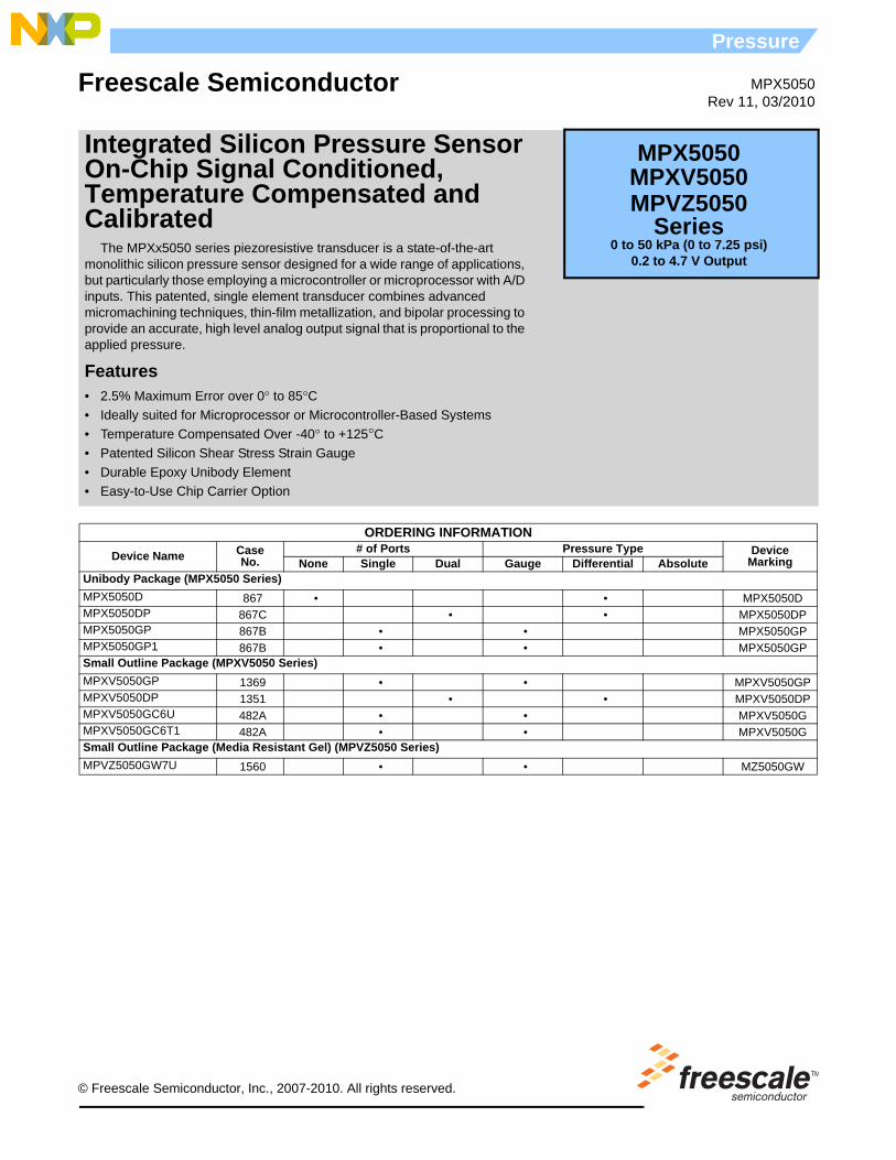
Integrated Silicon Pressure Sensor On-Chip Signal Conditioned, Temperature Compensated and Calibrated
The MPXx5050 series piezoresistive transducer is a state-of-the-art monolithic silicon pressure sensor designed for a wide range of applications, but particularly those employing a microcontroller or microprocessor with A/D inputs. This patented, single element transducer combines advanced micromachining techniques, thin-film metallization, and bipolar processing to provide an accurate, high level analog output signal that is proportional to the applied pressure.
Features• 2.5% Maximum Error over 0° to 85°C• Ideally suited for Microprocessor or Microcontroller-Based Systems• Temperature Compensated Over -40° to +125°C• Patented Silicon Shear Stress Strain Gauge• Durable Epoxy Unibody Element• Easy-to-Use Chip Carrier Option
ORDERING INFORMATION
Device Name CaseNo.
# of Ports Pressure Type DeviceMarkingNone Single Dual Gauge Differential Absolute
Table 1. Operating Characteristics (VS = 5.0 Vdc, TA = 25°C unless otherwise noted, P1 > P2. Decoupling circuit shown in Figure 4 required to meet electrical specifications.)
Characteristic Symbol Min Typ Max Unit
Pressure Range(1)
1. 1.0 kPa (kiloPascal) equals 0.145 psi.
POP 0 — 50 kPa
Supply Voltage(2)
2.Device is ratiometric within this specified excitation range.
VS 4.75 5.0 5.25 Vdc
Supply Current Io — 7.0 10 mAdc
Minimum Pressure Offset(3) (0 to 85°C)@ VS = 5.0 Volts
3.Offset (Voff) is defined as the output voltage at the minimum rated pressure.
Voff 0.088 0.2 0.313 Vdc
Full Scale Output(4) (0 to 85°C)@ VS = 5.0 Volts
4.Full Scale Output (VFSO) is defined as the output voltage at the maximum or full rated pressure.
VFSO 4.587 4.7 4.813 Vdc
Full Scale Span(5) (0 to 85°C)@ VS = 5.0 Volts
5.Full Scale Span (VFSS) is defined as the algebraic difference between the output voltage at full rated pressure and the output voltage at the minimum rated pressure.
VFSS — 4.5 — Vdc
Accuracy(6) (0 to 85°C)
6.Accuracy (error budget) consists of the following:Linearity: Output deviation from a straight line relationship with pressure over the specified pressure range.Temperature Hysteresis: Output deviation at any temperature within the operating temperature range, after the temperature is cycled to and from the minimum or maximum operating temperature points, with zero differential pressure applied.Pressure Hysteresis: Output deviation at any pressure within the specified range, when this pressure is cycled to and from the minimum or maximum rated pressure at 25°C.TcSpan: Output deviation over the temperature range of 0° to 85°C, relative to 25°C.TcOffset: Output deviation with minimum pressure applied, over the temperature range of 0° to 85°C, relative to 25°C.Variation from Nominal: The variation from nominal values, for Offset or Full Scale Span, as a percent of VFSS at 25°C.
— — — ±2.5 %VFSS
Sensitivity V/P — 90 — mV/kPa
Response Time(7)
7.Response Time is defined as the time for the incremental change in the output to go from 10% to 90% of its final value when subjected to a specified step change in pressure.
tR — 1.0 — ms
Output Source Current at Full Scale Output Io+ — 0.1 — mAdc
Warm-Up Time(8)
8.Warm-up Time is defined as the time required for the product to meet the specified output voltage after the Pressure has been stabilized.
— — 20 — ms
Offset Stability(9)
9.Offset Stability is the product's output deviation when subjected to 1000 hours of Pulsed Pressure, Temperature Cycling with Bias Test.
— — ±0.5 — %VFSS
MPX5050
SensorsFreescale Semiconductor 3
Pressure
Maximum Ratings
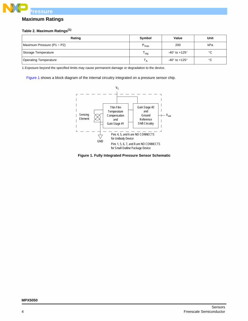
Figure 1 shows a block diagram of the internal circuitry integrated on a pressure sensor chip.
1.Exposure beyond the specified limits may cause permanent damage or degradation to the device.
Rating Symbol Value Unit
Maximum Pressure (P1 > P2) Pmax 200 kPa
Storage Temperature Tstg -40° to +125° °C
Operating Temperature TA -40° to +125° °C
SensingElement
Thin FilmTemperature
Compensationand
Gain Stage #1
Gain Stage #2and
GroundReference
Shift Circuitry
VS
Vout
GND
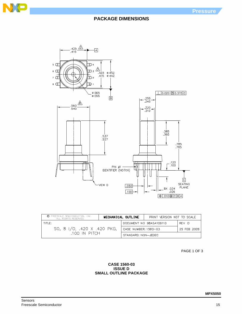
Pins 4, 5, and 6 are NO CONNECTSfor Unibody DevicePins 1, 5, 6, 7, and 8 are NO CONNECTSfor Small Outline Package Device
MPX5050
Sensors4 Freescale Semiconductor
Pressure
On-chip Temperature Compensation and Calibration
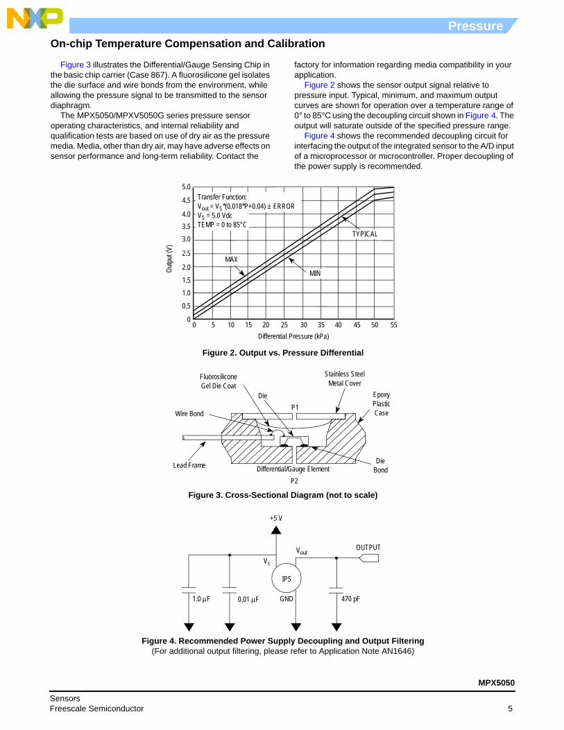
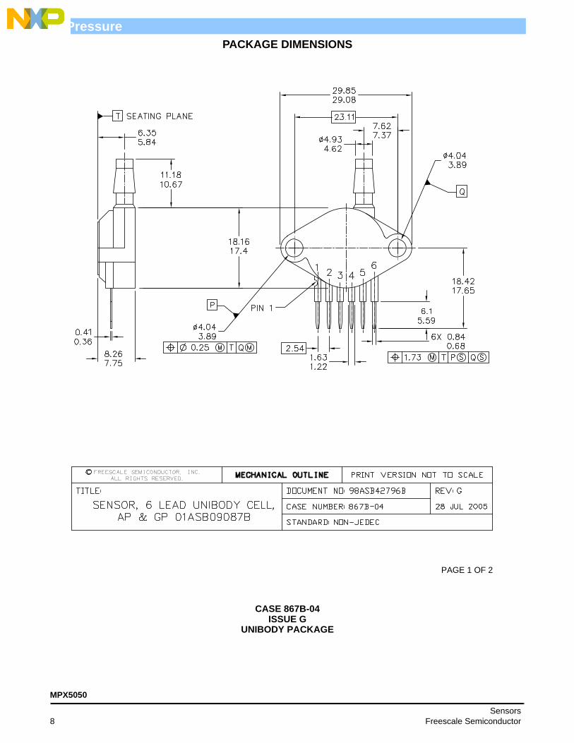
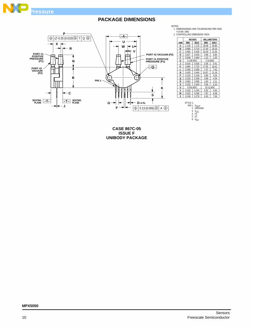
Figure 3 illustrates the Differential/Gauge Sensing Chip in the basic chip carrier (Case 867). A fluorosilicone gel isolates the die surface and wire bonds from the environment, while allowing the pressure signal to be transmitted to the sensor diaphragm.
The MPX5050/MPXV5050G series pressure sensor operating characteristics, and internal reliability and qualification tests are based on use of dry air as the pressure media. Media, other than dry air, may have adverse effects on sensor performance and long-term reliability. Contact the
factory for information regarding media compatibility in your application.
Figure 2 shows the sensor output signal relative to pressure input. Typical, minimum, and maximum output curves are shown for operation over a temperature range of 0° to 85°C using the decoupling circuit shown in Figure 4. The output will saturate outside of the specified pressure range.
Figure 4 shows the recommended decoupling circuit for interfacing the output of the integrated sensor to the A/D input of a microprocessor or microcontroller. Proper decoupling of the power supply is recommended.
Figure 2. Output vs. Pressure Differential
Figure 3. Cross-Sectional Diagram (not to scale)
Figure 4. Recommended Power Supply Decoupling and Output Filtering(For additional output filtering, please refer to Application Note AN1646)
Differential Pressure (kPa)
Outpu
t (V)
5.0
4.5
4.03.53.0
2.5
2.0
1.51.0
0.5
00 5 10 15 20 25 30 35 40 45 5550
Transfer Function: Vout = VS*(0.018*P+0.04) ± ERRORVS = 5.0 VdcTEMP = 0 to 85°C
TYPICAL
MIN
MAX
FluorosiliconeGel Die Coat
Wire Bond
DieP1
Stainless SteelMetal Cover
Lead Frame DieBond
EpoxyPlasticCase
P2Differential/Gauge Element
+5 V
1.0 μF 0.01 μF 470 pFGND
Vs
Vout
IPS
OUTPUT
MPX5050
SensorsFreescale Semiconductor 5
Pressure
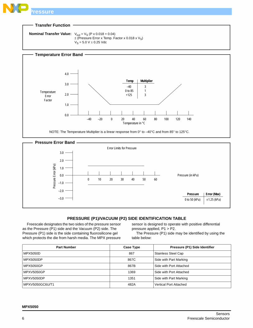
PRESSURE (P1)/VACUUM (P2) SIDE IDENTIFICATION TABLEFreescale designates the two sides of the pressure sensor
as the Pressure (P1) side and the Vacuum (P2) side. The Pressure (P1) side is the side containing fluorosilicone gel which protects the die from harsh media. The MPX pressure
sensor is designed to operate with positive differential pressure applied, P1 > P2.
The Pressure (P1) side may be identified by using the table below:
Nominal Transfer Value: Vout = VS (P x 0.018 + 0.04)± (Pressure Error x Temp. Factor x 0.018 x VS)VS = 5.0 V ± 0.25 Vdc
Transfer Function
Temp Multiplier –40 3 0 to 85 1 +125 3
Temperature in °C
4.0
3.0
2.0
0.0
1.0
–40 –20 0 20 40 60 14012010080
TemperatureError
Factor
NOTE: The Temperature Multiplier is a linear response from 0° to –40°C and from 85° to 125°C.
Temperature Error Band
Pressure Error (Max)
Pressure Error Band
0 to 50 (kPa) ±1.25 (kPa)
Error Limits for Pressure
Pressure (in kPa)
3.0
2.0
1.0
–1.0
–2.0
–3.0
0.00 10 20 30 40 50 60
Pres
sure
Erro
r (kP
a)
Part Number Case Type Pressure (P1) Side Identifier
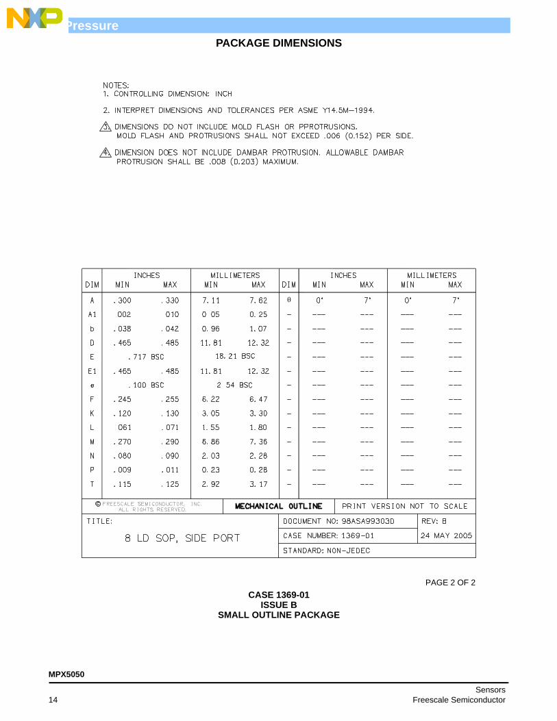
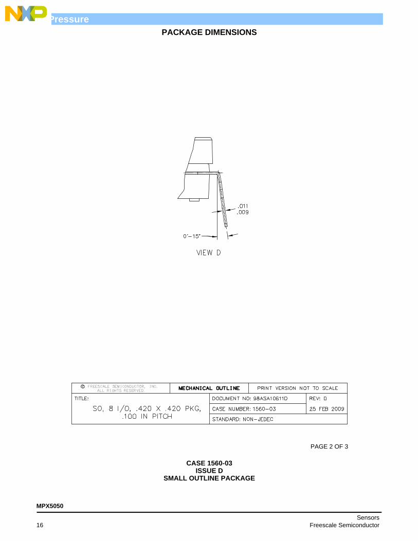
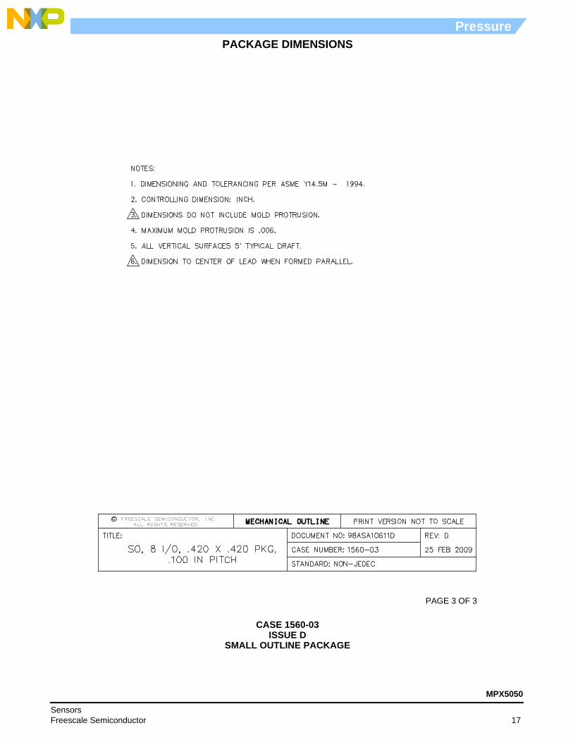
Y14.5M, 1982.2. CONTROLLING DIMENSION: INCH.3. DIMENSION A AND B DO NOT INCLUDE MOLD
PROTRUSION.4. MAXIMUM MOLD PROTRUSION 0.15 (0.006).5. ALL VERTICAL SURFACES 5 TYPICAL DRAFT.
S
D
G
8 PL
45
81
SBM0.25 (0.010) A ST
–A–
–B–
C
M
J
KPIN 1 IDENTIFIER
H
SEATINGPLANE
–T–
N
V
W
V 0.245 0.255 6.22 6.48W 0.115 0.125 2.92 3.17
PIN 1
FG
NL
R
1 2 3 4 5 6
6 PLD
SEATINGPLANE -T-
MAM0.136 (0.005) T
POSITIVE PRESSURE(P1)
C
B
M
JS
-A-
STYLE 1: PIN 1. VOUT
2. GROUND 3. VCC 4. V1 5. V2 6. VEX
STYLE 3: PIN 1. OPEN
2. GROUND 3. +VOUT 4. +VSUPPLY 5. -VOUT 6. OPEN
STYLE 2: PIN 1. OPEN
2. GROUND 3. -VOUT 4. VSUPPLY 5. +VOUT 6. OPEN
MAXMILLIMETERSINCHES
16.0013.565.590.841.63
0.100 BSC 2.54 BSC0.40
18.4230˚ NOM 30˚ NOM
12.5711.43
DIMABCDFGJLMNRS
MIN0.5950.5140.2000.0270.048
0.0140.695
0.4750.4300.090
MAX0.6300.5340.2200.0330.064
0.0160.725
0.4950.4500.105
MIN15.1113.065.080.681.22
0.3617.65
12.0710.922.29 2.66
NOTES:1.
2.3.
DIMENSIONING AND TOLERANCING PER ANSI Y14.5M, 1982.CONTROLLING DIMENSION: INCH.DIMENSION -A- IS INCLUSIVE OF THE MOLDSTOP RING. MOLD STOP RING NOT TO EXCEED16.00 (0.630).
USA/Europe or Locations Not Listed:Freescale Semiconductor, Inc.Technical Information Center, EL5162100 East Elliot RoadTempe, Arizona 852841-800-521-6274 or +1-480-768-2130www.freescale.com/support
Europe, Middle East, and Africa:Freescale Halbleiter Deutschland GmbHTechnical Information CenterSchatzbogen 781829 Muenchen, Germany+44 1296 380 456 (English)+46 8 52200080 (English)+49 89 92103 559 (German)+33 1 69 35 48 48 (French)www.freescale.com/support
Japan:Freescale Semiconductor Japan Ltd.HeadquartersARCO Tower 15F1-8-1, Shimo-Meguro, Meguro-ku,Tokyo 153-0064Japan0120 191014 or +81 3 5437 [email protected]
Asia/Pacific:Freescale Semiconductor China Ltd.Exchange Building 23FNo. 118 Jianguo RoadChaoyang DistrictBeijing 100022 China +86 10 5879 [email protected]
For Literature Requests Only:Freescale Semiconductor Literature Distribution Center1-800-441-2447 or +1-303-675-2140Fax: [email protected]
Information in this document is provided solely to enable system and software implementers to use Freescale Semiconductor products. There are no express or implied copyright licenses granted hereunder to design or fabricate any integrated circuits or integrated circuits based on the information in this document.
Freescale Semiconductor reserves the right to make changes without further notice to any products herein. Freescale Semiconductor makes no warranty, representation or guarantee regarding the suitability of its products for any particular purpose, nor does Freescale Semiconductor assume any liability arising out of the application or use of any product or circuit, and specifically disclaims any and all liability, including without limitation consequential or incidental damages. “Typical” parameters that may be provided in Freescale Semiconductor data sheets and/or specifications can and do vary in different applications and actual performance may vary over time. All operating parameters, including “Typicals”, must be validated for each customer application by customer’s technical experts. Freescale Semiconductor does not convey any license under its patent rights nor the rights of others. Freescale Semiconductor products are not designed, intended, or authorized for use as components in systems intended for surgical implant into the body, or other applications intended to support or sustain life, or for any other application in which the failure of the Freescale Semiconductor product could create a situation where personal injury or death may occur. Should Buyer purchase or use Freescale Semiconductor products for any such unintended or unauthorized application, Buyer shall indemnify and hold Freescale Semiconductor and its officers, employees, subsidiaries, affiliates, and distributors harmless against all claims, costs, damages, and expenses, and reasonable attorney fees arising out of, directly or indirectly, any claim of personal injury or death associated with such unintended or unauthorized use, even if such claim alleges that Freescale Semiconductor was negligent regarding the design or manufacture of the part.