16
MSP430-H2618 development board Users Manual All boards produced by Olimex are RoHS compliant Rev. Initial, April 2009 Copyright(c) 2009, OLIMEX Ltd, All rights reserved Page 1

MSP430-H2618 development board Users Manual
All boards produced by Olimex are RoHS compliant
Rev. Initial, April 2009Copyright(c) 2009, OLIMEX Ltd, All rights reserved
Page 1

INTRODUCTION:
MSP430-H2618 header board provides easy way for developing and prototyping with the new mixed signal MSP430F2618 microcontroller. It has JTAG interface and most of the GPIOs are on extension headers where you can connect your additional circuits.
BOARD FEATURES:
− MCU: MSP430F2618 with 116 KB + 256 B Flash Memory, 8 KB RAM− JTAG connector − 32 768 Hz oscillator crystal− Optional high frequency crystal (socket)− Extension headers for all microcontroller pins− PCB: FR-4, 1.5 mm (0.062''), green soldermask, silkscreen component print − Dimensions 46.99 x 46.99 mm (1.850 x 1.850")
ELECTROSTATIC WARNING:
The MSP430-H2618 board is shipped in protective anti-static packaging. The board must not be subject to high electrostatic potentials. General practice for working with static sensitive devices should be applied when working with this board.
BOARD USE REQUIREMENTS:
Cables: The cable you will need depends on the programmer/debugger you use. If you use MSP430-JTAG, you will need LPT cable. You will need 1.8 meter USB A-B cable to connect MSP430-JTAG-ISO or MSP430-JTAG-TINY to a USB host on your PC. If you use MSP430-JTAG-RF, you will not need a cable.
Hardware: Programmer/Debugger – one of the Olimex MSP430-JTAG tools: MSP430-JTAG, MSP430-JTAG-ISO, MSP430-JTAG-TINY, MSP430-JTAG-RF.
Software: Olimex MSP430 programmer – free stand-alone software which allows you to program MSP430 devices without any third party software; MSP430 Kick Start C compiler and debugger (free for assembly, limited for C); MSPGCC – free compiler and debugger. You will also need drivers for the JTAG programmer that you use (to be found on the corresponding web pages on our web site).
Page 2

PROCESSOR FEATURES:
MSP430-H2618 board uses MCU MSP430F2618 from Texas Instruments with these features:
- Low Supply Voltage Range, 1.8 V to 3.6 V- Ultra-Low Power Consumption:
- Active Mode: 365 µA at 1 MHz, 2.2 V- Standby Mode: 0.5 µA- Off Mode (RAM Retention): 0.1 µA
- Wake-Up From Standby Mode in Less Than 1µs- 16-Bit RISC Architecture, 62.5-ns Instruction Cycle Time- Three-Channel Internal DMA- 12-Bit Analog-to-Digital (A/D) Converter With Internal Reference,
Sample-and-Hold, and Autoscan Feature- Dual 12-Bit Digital-to-Analog (D/A) Converters With Synchronization- 16-Bit Timer_A With Three Capture/Compare Registers- 16-Bit Timer_B With Seven Capture/Compare-With-Shadow Registers- On-Chip Comparator- Four Universal Serial Communication Interfaces (USCIs)
- USCI_A0 and USCI_A1- Enhanced UART Supporting Auto-Baudrate Detection- IrDA Encoder and Decoder- Synchronous SPI
- USCI_B0 and USCI_B1- I2C- Synchronous SPI
- Supply Voltage Supervisor/Monitor With Programmable Level Detection- Brownout Detector- Bootstrap Loader- Serial Onboard Programming, No External Programming Voltage Needed
Programmable Code Protection by Security Fuse- 116KB+256B Flash Memory, 8KB RAM
Page 3

BLOCK DIAGRAM:
Page 4

MEMORY MAP:
Page 5

SCHEMATIC:
Page 6
10uF(NA)
100nF
10nF
100nF
10pF
10pF
20pF 20pF
P_IN P_OUT
32KHz
455KHz-8MHz(NA)
47K
NA NA
MSP430F2618
C1
C2
C3
C4
C5
C6
C7 C8
12345678910111213141516
CON1
12345678910111213141516
CON2
123456789
10111213141516
CON3
123456789
10111213141516
CON4
12
12
1234567891011121314
JTAG
Q1
Q2
Q3
R1
R2 R3
123456789
1011121314151617181920212223242526272829303132 33
34353637383940414243444546474849505152535455565758596061626364
U1
MSP430-H2618Rev. Initial
COPYRIGHT(C) 2009
WWW.OLIMEX.COM/DEV
+

BOARD LAYOUT:
POWER SUPPLY CIRCUIT:
MSP430-H2618 is typically power supplied from the JTAG interface (P_IN closed). If not, you could power supply the board if you apply up to +3.6VDC at CON1 pin 1 (MSP430F2618.pin 1) and GND at CON4 pin 14 or pin 15 (MSP430F2618.pin 62 or 63).
The board power consumption is less than 10 mA.
RESET CIRCUIT:
MSP430-H2618 reset circuit is realized with a pull-up resistor R1 (47k) and capacitor C3(10n). You could also reset the MCU with an active low level at the JTAG pin 11 or at CON4 pin 10 (MSP430F2618.pin 58).
Page 7

CLOCK CIRCUIT:
Quartz crystal 32 768 Hz is connected to MSP430F2618 pin 8 (XIN) and pin 9 (XOUT/TCLK).
There is an option for a high speed crystal oscillator to be connected to the MSP430F2618 pin 52 (XT2OUT) and pin 53 (XT2IN).
JUMPER DESCRIPTION:
P_INWhen this jumper is closed, the board is power supplied by the standard JTAG pin 2. This is only possible when the consumption of the board is not very high which is typically the case with MSP430 microcontrollers. If this jumper is open the board should be power supplied by another external source. This jumper and P_OUT should always be reversely open/closed, i.e. if P_IN is closed, P_OUT should be open and vice versa. Default state is closed.
P_OUTWhen this jumper is closed, the board is power supplied not by the JTAG but from external source. Then the JTAG has to synchronize with the working voltages which is done through this line. This is especially important when debugging with JTAG. This jumper and P_IN should always be reversely open/closed, i.e. if P_OUT is closed, P_IN should be open and vice versa.
Default state is open.
Page 8
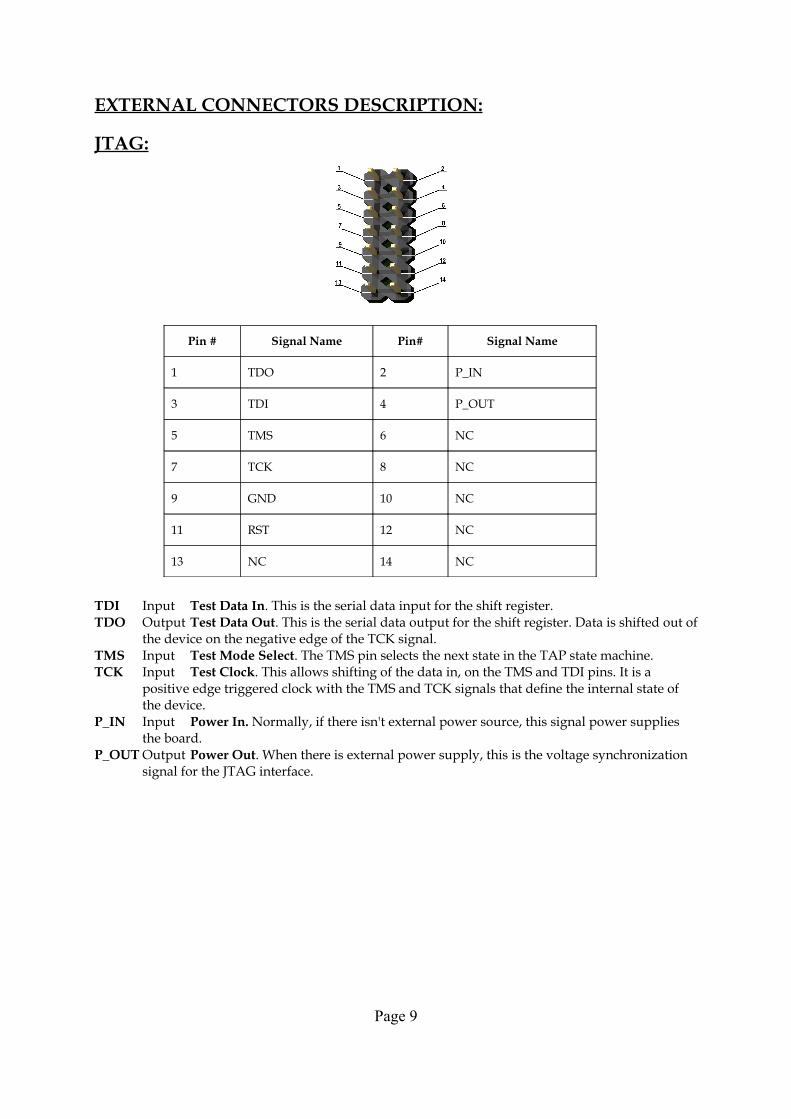
EXTERNAL CONNECTORS DESCRIPTION:
JTAG:
Pin # Signal Name Pin# Signal Name
1 TDO 2 P_IN
3 TDI 4 P_OUT
5 TMS 6 NC
7 TCK 8 NC
9 GND 10 NC
11 RST 12 NC
13 NC 14 NC
TDI Input Test Data In. This is the serial data input for the shift register.TDO Output Test Data Out. This is the serial data output for the shift register. Data is shifted out of
the device on the negative edge of the TCK signal.TMS Input Test Mode Select. The TMS pin selects the next state in the TAP state machine.TCK Input Test Clock. This allows shifting of the data in, on the TMS and TDI pins. It is a
positive edge triggered clock with the TMS and TCK signals that define the internal state of the device.
P_IN Input Power In. Normally, if there isn't external power source, this signal power supplies the board.
P_OUT Output Power Out. When there is external power supply, this is the voltage synchronization signal for the JTAG interface.
Page 9

CON1:
Pin # Signal Name Pin# Signal Name
1 (1) DVCC1 2 (2) P6.3/A3
3 (3) P6.4/A4 4 (4) P6.5/A5/DAC1
5 (5) P6.6/A6/DAC0 6 (6) P6.7/A7/DAC1/SVSIN
7 (7) VREF+ 8 (8) XIN
9 (9) XOUT 10 (10) VeREF+/DAC0
11 (11) VREF-/VeREF- 12 (12) P1.0/TACLK/CAOUT
13 (13) P1.1/TA0 14 (14) P1.2/TA1
15 (15) P1.3/TA2 16 (16) P1.4/SMCLK
CON2:
Pin # Signal Name Pin# Signal Name
1 (17) P1.5/TA0 2 (18) P1.6/TA1
3 (19) P1.7/TA2 4 (20) P2.0/ACLK/CA2
5 (21) P2.1/TAINCLK/CA3 6 (22) P2.2/CAOUT/TA0/CA4
7 (23) P2.3/CA0/TA1 8 (24) P2.4/CA1/TA2
9 (25) P2.5/Rosc/CA5 10 (26) P2.6/ADC12CLK/CA6
11 (27) P2.7/TA0/CA7 12 (28) P3.0/UCB0STE
13 (29) P3.1/UCB0SIMO/UCB0SD 14 (30) P3.2/UCB0SOMI/UCB0SC
Page 10

A L
15 (31) P3.3/UCB0CLK/UCA0STE 16 (32) P3.4/UCA0TXD
UCB0CLK I/O Universal Serial Communication Interface (USCI) B0 clock input/output.UCB0SOMI I/O USCI B0 slave out/master in in SPI mode.UCB0SIMO I/O USCI B0 slave in/master out in SPI mode.UCB0STE I/O USCI B0 slave transmit enable.UCA0TXD Output USCIA transmit data output in UART mode.UCB0SDA I/O SDA I2C data in I2C mode.USB0SCL I/O SCL I2C clock in I2C mode.
CON3:
Pin # Signal Name Pin# Signal Name
1 (33) P3.5/UCA0RXD 2 (34) P3.6/UCA1TXD
3 (35) P3.7/UCA1RXD 4 (36) P4.0/TB0
5 (37) P4.1/TB1 6 (38) P4.2/TB2
7 (39) P4.3/TB3 8 (40) P4.4/TB4
9 (41) P4.5/TB5 10 (42) P4.6/TB6
11 (43) P4.7/TBCLK 12 (44) P5.0/UCB1STE
13 (45) P5.1/UCB1SIMO 14 (46) P5.2/UCB1SOMI
15 (47) P5.3/UCB1CLK 16 (48) P5.4/MCLK
UCA0RXD Input USCI A0 receive data input in UART mode, slave data out.UCB1CLK I/O USCI B1 clock input/output.UCB1SOMI I/O USCI B1 slave out/master in in SPImode.UCB1SIMO I/O USCI B1slave in/master out in SPI mode.UCB1STE I/O USCI B1 slave transmit enable.UCA1TXD Output USCI A1 transmit data output in UART mode.UCA1RXD Input USCI A1 receive data input in UART mode.
Page 11

CON4:
Pin # Signal Name Pin# Signal Name
1 (49) P5.5/SMCLK 2 (50) P5.6/ACLK
3 (51) P5.7/TBOUTH/SVSOUT
4 (52) XT2OUT
5 (53) XT2IN 6 (54) TDO/TDI
7 (55) TDI/TCLK 8 (56) TMS
9 (57) TCK 10 (58) #RST/NMI
11 (59) P6.0/A0 12 (60) P6.1/A1
13 (61) P6.2/A2 14 (62) AVSS
15 (63) DVSS1 16 (64) AVCC
Page 12

MECHANICAL DIMENSIONS:
- All measures are in inches.
Page 13

AVAILABLE DEMO SOFTWARE :
– MSP430-H2618_Blinking_Led
You could find MSP430-H2618 demo software at www.olimex.com/dev .
Page 14
ORDER CODE:
MSP430-H2618 – assembled and tested (no kit, no soldering required).
How to order? You can order to us directly or by any of our distributors. Check our web www.olimex.com/dev for more info.
Revision history:
REV. Initial - created April 2009
Page 15
Disclaimer: © 2009 Olimex Ltd. All rights reserved. Olimex®, logo and combinations thereof, are registered trademarks of Olimex Ltd. Other terms and product names may be trademarks of others.The information in this document is provided in connection with Olimex products. No license, express or implied or otherwise, to any intellectual property right is granted by this document or in connection with the sale of Olimex products. Neither the whole nor any part of the information contained in or the product described in this document may be adapted or reproduced in any material from except with the prior written permission of the copyright holder.The product described in this document is subject to continuous development and improvements. All particulars of the product and its use contained in this document are given by OLIMEX in good faith. However all warranties implied or expressed including but not limited to implied warranties of merchantability or fitness for purpose are excluded.This document is intended only to assist the reader in the use of the product. OLIMEX Ltd. shall not be liable for any loss or damage arising from the use of any information in this document or any error or omission in such information or any incorrect use of the product.
Page 16


