30
April 1999 Mixed Signal Products Application Report SLAA049
���� ��������� �����������
������������ �������� �������
������������� ���������
April 1999 Mixed Signal Products
ApplicationReport
SLAA049
IMPORTANT NOTICE
Texas Instruments and its subsidiaries (TI) reserve the right to make changes to their products or to discontinueany product or service without notice, and advise customers to obtain the latest version of relevant informationto verify, before placing orders, that information being relied on is current and complete. All products are soldsubject to the terms and conditions of sale supplied at the time of order acknowledgement, including thosepertaining to warranty, patent infringement, and limitation of liability.
TI warrants performance of its semiconductor products to the specifications applicable at the time of sale inaccordance with TI’s standard warranty. Testing and other quality control techniques are utilized to the extentTI deems necessary to support this warranty. Specific testing of all parameters of each device is not necessarilyperformed, except those mandated by government requirements.
CERTAIN APPLICATIONS USING SEMICONDUCTOR PRODUCTS MAY INVOLVE POTENTIAL RISKS OFDEATH, PERSONAL INJURY, OR SEVERE PROPERTY OR ENVIRONMENTAL DAMAGE (“CRITICALAPPLICATIONS”). TI SEMICONDUCTOR PRODUCTS ARE NOT DESIGNED, AUTHORIZED, ORWARRANTED TO BE SUITABLE FOR USE IN LIFE-SUPPORT DEVICES OR SYSTEMS OR OTHERCRITICAL APPLICATIONS. INCLUSION OF TI PRODUCTS IN SUCH APPLICATIONS IS UNDERSTOOD TOBE FULLY AT THE CUSTOMER’S RISK.
In order to minimize risks associated with the customer’s applications, adequate design and operatingsafeguards must be provided by the customer to minimize inherent or procedural hazards.
TI assumes no liability for applications assistance or customer product design. TI does not warrant or representthat any license, either express or implied, is granted under any patent right, copyright, mask work right, or otherintellectual property right of TI covering or relating to any combination, machine, or process in which suchsemiconductor products or services might be or are used. TI’s publication of information regarding any thirdparty’s products or services does not constitute TI’s approval, warranty or endorsement thereof.
Copyright 1999, Texas Instruments Incorporated
iii MSP430 Universal Synchronous Asynchronous Receive/Transmit Communication Interface
Contents1 Introduction 1. . . . . . . . . . . . . . . . . . . . . . . . . . . . . . . . . . . . . . . . . . . . . . . . . . . . . . . . . . . . . . . . . . . . . . . . . . . . . . . . . . .
1.1 Attributes of the MSP430 UART 3. . . . . . . . . . . . . . . . . . . . . . . . . . . . . . . . . . . . . . . . . . . . . . . . . . . . . . . . . . . . 1.2 Data Format 3. . . . . . . . . . . . . . . . . . . . . . . . . . . . . . . . . . . . . . . . . . . . . . . . . . . . . . . . . . . . . . . . . . . . . . . . . . . . . 1.3 UART Hardware Registers 4. . . . . . . . . . . . . . . . . . . . . . . . . . . . . . . . . . . . . . . . . . . . . . . . . . . . . . . . . . . . . . . . .
2 Baud Rate Generation 6. . . . . . . . . . . . . . . . . . . . . . . . . . . . . . . . . . . . . . . . . . . . . . . . . . . . . . . . . . . . . . . . . . . . . . . . . . 2.1 Baud Rate Generation With the MCLK 8. . . . . . . . . . . . . . . . . . . . . . . . . . . . . . . . . . . . . . . . . . . . . . . . . . . . . . 2.2 Baud Rate Generation With the ACLK 9. . . . . . . . . . . . . . . . . . . . . . . . . . . . . . . . . . . . . . . . . . . . . . . . . . . . . . .
3 Software Routines 10. . . . . . . . . . . . . . . . . . . . . . . . . . . . . . . . . . . . . . . . . . . . . . . . . . . . . . . . . . . . . . . . . . . . . . . . . . . . 3.1 Non-Interrupt Processing 10. . . . . . . . . . . . . . . . . . . . . . . . . . . . . . . . . . . . . . . . . . . . . . . . . . . . . . . . . . . . . . . . . 3.2 Interrupt Processing 12. . . . . . . . . . . . . . . . . . . . . . . . . . . . . . . . . . . . . . . . . . . . . . . . . . . . . . . . . . . . . . . . . . . . .
3.2.1 MCLK Used as UART Clock 12. . . . . . . . . . . . . . . . . . . . . . . . . . . . . . . . . . . . . . . . . . . . . . . . . . . . . . . 3.2.2 ACLK Used as UART Clock 16. . . . . . . . . . . . . . . . . . . . . . . . . . . . . . . . . . . . . . . . . . . . . . . . . . . . . . .
3.3 Subroutines and .MACROs 20. . . . . . . . . . . . . . . . . . . . . . . . . . . . . . . . . . . . . . . . . . . . . . . . . . . . . . . . . . . . . . . 3.3.1 Subroutines 20. . . . . . . . . . . . . . . . . . . . . . . . . . . . . . . . . . . . . . . . . . . . . . . . . . . . . . . . . . . . . . . . . . . . . 3.3.2 .MACROs 21. . . . . . . . . . . . . . . . . . . . . . . . . . . . . . . . . . . . . . . . . . . . . . . . . . . . . . . . . . . . . . . . . . . . . . .
4 References 24. . . . . . . . . . . . . . . . . . . . . . . . . . . . . . . . . . . . . . . . . . . . . . . . . . . . . . . . . . . . . . . . . . . . . . . . . . . . . . . . . . .
Appendix A Definitions A-1. . . . . . . . . . . . . . . . . . . . . . . . . . . . . . . . . . . . . . . . . . . . . . . . . . . . . . . . . . . . . . . . . . . . . . . .
List of Figures1 MSP430 USART Module 2. . . . . . . . . . . . . . . . . . . . . . . . . . . . . . . . . . . . . . . . . . . . . . . . . . . . . . . . . . . . . . . . . . . . . . . . . . 2 USART Switched to the UART Mode 3. . . . . . . . . . . . . . . . . . . . . . . . . . . . . . . . . . . . . . . . . . . . . . . . . . . . . . . . . . . . . . . 3 RS232 Format (Levels at the MSP430) 4. . . . . . . . . . . . . . . . . . . . . . . . . . . . . . . . . . . . . . . . . . . . . . . . . . . . . . . . . . . . . 4 RS232 Format (Levels on the Transmission Line) 4. . . . . . . . . . . . . . . . . . . . . . . . . . . . . . . . . . . . . . . . . . . . . . . . . . . . 5 USART Control Registers Used in the UART Mode 5. . . . . . . . . . . . . . . . . . . . . . . . . . . . . . . . . . . . . . . . . . . . . . . . . . . 6 Baud Rate Generator 6. . . . . . . . . . . . . . . . . . . . . . . . . . . . . . . . . . . . . . . . . . . . . . . . . . . . . . . . . . . . . . . . . . . . . . . . . . . . . 7 Function of the Baud Rate Correction 8. . . . . . . . . . . . . . . . . . . . . . . . . . . . . . . . . . . . . . . . . . . . . . . . . . . . . . . . . . . . . . .
List of Tables1 Content of Baud Rate Registers UBR (MCLK = 1.048 MHz) 9. . . . . . . . . . . . . . . . . . . . . . . . . . . . . . . . . . . . . . . . . . . 2 Content of Baud Rate Registers UBR (ACLK = 32,768 Hz) 10. . . . . . . . . . . . . . . . . . . . . . . . . . . . . . . . . . . . . . . . . . .

iv SLAA049
1
MSP430 Universal Synchronous Asynchronous Receive/TransmitCommunication Interface
Lutz Bierl
ABSTRACTThis application report gives a short overview for the use of the MSP430 universalsynchronous, asynchronous receive/transmit communication interface (USART) as anRS232 interface, also called a serial-controller interface (SCI). Tested softwareexamples, with and without the use of the interrupt capability, are given for thetransmission and the reception of UART (universal asynchronous receive/transmit)signals. Full duplex mode is used for all examples running in active mode and low powermode 3 (LPM3).
1 IntroductionThe universal synchronous/asynchronous receive/transmit communicationinterface of the MSP430 family can operate in two different modes: synchronousand asynchronous. This application report describes the software routines usedwith the asynchronous mode (SCI, RS232). A second report will handle thesynchronous mode (serial protocol interface SPI).
NOTE: Reading the data book MSP430 Family ArchitectureGuide and Module Library is recommended. It complements theinformation contained in this application report.
NOTE: The examples and hardware definitions useMSP430x33x addresses. Future MSP430 family members mayhave different hardware addresses—especially for the I/O portsused.
The hardware features of the USART module greatly exceed the capabilitiesillustrated in the examples included in this application report. This report isintended as a fast way to get the USART running in the UART mode, with orwithout the interrupt capability. Features frequently used are included in theexamples.

Introduction
2 SLAA049
Figure 1 shows the block diagram of the MSP430 USART module.
0
Receive Buffer URXBUF
SSEL0SSEL1
UCLKI
ACLK
MCLK
1
2
3MCLK
WUT
CKPH
Receive Shift Register
Receive Status
0
SYNC
SYNC
Baud Rate Generator
Baud Rate Register UBR
Baud Rate Generator
SYNCSYNC
SYNCUCLKS
Transmit Shift Register
Transmit Buffer UTXBUF
0
1
1
0
1
0
Clock Phase and Polarity
SYNC CKPL
UCLKI
UCLKS
UCLK
SIMO
UTXD
STE
URXD
SOMI
MMListenSYNC RXE
TXWake
Control Registers
Figure 1. MSP430 USART Module

Introduction
3 MSP430 Universal Synchronous Asynchronous Receive/Transmit Communication Interface
Figure 2 shows the situation when the USART is switched to the UART mode bysetting the SYNC bit UCTL.2 to zero
0
Receive Buffer URXBUF
SSEL0SSEL1
UCLKI
ACLK
MCLK
1
2
3MCLK
WUT
Receive Shift Register
Receive Status
LSB first
Baud Rate Generator
Baud Rate Register UBR
Baud Rate Generator
UCLKS
Transmit Shift Register
Transmit Buffer UTXBUF
0
1
Clock Polarity
CKPL
UCLKI
UCLKSUCLK
URXD
SYNC = 0
ListenRXE
TXWake
UTXD
Control Registers
Data
Data
Figure 2. USART Switched to the UART Mode
1.1 Attributes of the MSP430 UARTThe following is a short overview of the USART running in the UART mode:• Selectable seven and eight-bit data lengths• The error detection for the receive path is as follows:
– Frame error. The stop bits have space potential.– Parity error. Parity is enabled and the parity bit has the wrong value.– Overrun error. The next character is read in before the last one is read out
by the software.– Break detect. The URXD pin has low potential for more than 10 bits.
• Baud-rate generation made possible by 32-kHz crystal due to the modulationregister
• Interrupt-driven transmit and receive functions• Two independent interrupt vectors: one for transmission, one for reception• Full functionality during LPM3• End-of-frame flag usable with interrupt or polling
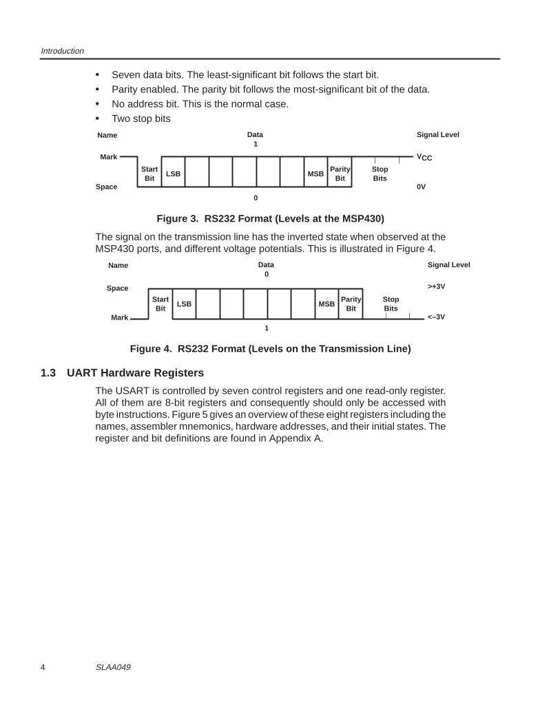
1.2 Data FormatThe data format used is RS232. Figure 3 shows how this format is seen at theMSP430 ports (URXD and UTXD), and Figure 4 shows how the format is definedon the transmission line. The format shown in Figures 3 and 4 has:
Introduction
4 SLAA049
• Seven data bits. The least-significant bit follows the start bit.
• Parity enabled. The parity bit follows the most-significant bit of the data.
• No address bit. This is the normal case.
• Two stop bits
Mark
Space
Name Data
VCC
Signal Level
0V
StartBit
LSB MSBParity
BitStopBits
1
0
Figure 3. RS232 Format (Levels at the MSP430)
The signal on the transmission line has the inverted state when observed at theMSP430 ports, and different voltage potentials. This is illustrated in Figure 4.
Mark
Space
Name Data
>+3V
Signal Level
<–3V
StartBit
LSB MSBParity
BitStopBits
0
1
Figure 4. RS232 Format (Levels on the Transmission Line)
1.3 UART Hardware Registers
The USART is controlled by seven control registers and one read-only register.All of them are 8-bit registers and consequently should only be accessed withbyte instructions. Figure 5 gives an overview of these eight registers including thenames, assembler mnemonics, hardware addresses, and their initial states. Theregister and bit definitions are found in Appendix A.

Introduction
5 MSP430 Universal Synchronous Asynchronous Receive/Transmit Communication Interface
Register Name Mnemonic Register Access Address Initial State
USART Control Register UCTL Read/Write 070h See below
Transmit Control Register UTCTL Read/Write 071h See below
Receive Control Register URCTL Read/Write 072h See below
Modulation Control Register UMCTL Read/Write 073h unchanged
Baud-Rate Register 0 UBR0 Read/Write 074h unchanged
Baud-Rate Register 1 UBR1 Read/Write 075h unchanged
Receive Buffer URXBUF Read Only 076h unchanged
Transmit Buffer UTXBUF Read/Write 077h unchanged
7 0 7 0
UCTL070h
PENA PEV SP CHAR Listen SYNC MM SWRSTUBR0074h
27 26 25 24 23 22 21 21
rw-0 rw-0 rw-0 rw-0 rw-0 rw-0 rw-0 rw-1 rw rw rw rw rw rw rw rw
7 0 7 0
UTCTL071
un-used
CKPLSSEL
1SSEL0 URXSE TXWake unused TXEPT
UBR1075h
215 214 213 212 211 210 29 28
rw-0 rw-0 rw-0 rw-0 rw-0 rw-0 rw-0 rw-1 rw rw rw rw rw rw rw rw
7 0 7 0
URCTL072h
FE PE OE BRK URXEIE URXWIE RXWake RXERRUMCTL
073hm7 m6 m5 m4 m3 m2 m1 m0
rw-0 rw-0 rw-0 rw-0 rw-0 rw-0 rw-0 rw-0 rw rw rw rw rw rw rw rw
7 0 7 0
URXBUF076h
27 26 25 24 23 22 21 20 UTXBUF077h
27 26 25 24 23 22 21 20
r r r r r r r r rw rw rw rw rw rw rw rw
Figure 5. USART Control Registers Used in the UART Mode
Baud Rate Generation
6 SLAA049
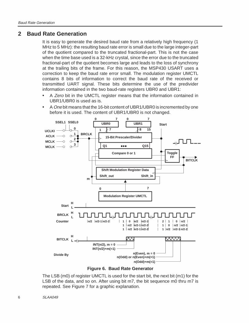
2 Baud Rate GenerationIt is easy to generate the desired baud rate from a relatively high frequency (1MHz to 5 MHz): the resulting baud rate error is small due to the large integer-partof the quotient compared to the truncated fractional-part. This is not the casewhen the time base used is a 32-kHz crystal, since the error due to the truncatedfractional-part of the quotient becomes large and leads to the loss of synchronyat the trailing bits of the frame. For this reason, the MSP430 USART uses acorrection to keep the baud rate error small. The modulation register UMCTLcontains 8 bits of information to correct the baud rate of the received ortransmitted UART signal. These bits determine the use of the predividerinformation contained in the two baud-rate registers UBR0 and UBR1:• A Zero bit in the UMCTL register means that the information contained in
UBR1/UBR0 is used as is.• A One bit means that the 16-bit content of UBR1/UBR0 is incremented by one
before it is used. The content of UBR1/UBR0 is not changed.
ÎÎÎÎ
ÎÎÎÎÎÎ
0
SSEL0SSEL1
UCLKI
ACLK
MCLK
1
2
3MCLK
15-Bit Prescaler/Divider
ToggleFF
Start
7 8 15
BITCLK
UBR0 UBR10 7 0 7
1
Q1 Q15
Compare 0 or 1
Shift Modulation Register Data
Shift_inShift_outm
Modulation Register UMCTL
70
BRCLK
INT(n/2), m = 0INT(n/2)+m(=1)
n(Even), m = 0n(Odd) or n(Even)+m(=1)
n(Odd)+m(=1)
HL
HL
HL
Start
BRCLK
Counter
BITCLK
Divide By
n/2-2n/2-1n/2 n/2-1n/201n/2-2n/2-1n/21n/2-2n/2-1n/21
n/2012n/2-1n/201n/2-2n/2-1n/21
Figure 6. Baud Rate Generator
The LSB (m0) of register UMCTL is used for the start bit, the next bit (m1) for theLSB of the data, and so on. After using bit m7, the bit sequence m0 thru m7 isrepeated. See Figure 7 for a graphic explanation.

Baud Rate Generation
7 MSP430 Universal Synchronous Asynchronous Receive/Transmit Communication Interface
EXAMPLE: a baud rate of 4800 baud is required with a crystal frequency of32,768 Hz. This is necessary because the UART also has to run during low powermode 3. With only the ACLK available, the theoretical division factor—thetruncated value is the content of baud-rate register UBR (UBR1/UBR0)—is:
UBR � 327684800
� 6.82667
This means that the baud-rate register UBR1 (MSBs) is loaded with zero, and theUBR0 register contains a 6. To get a rough estimate of the 8-bit modulationregister UMCTL, the fractional part 0.826667 is multiplied by 8 (the number of bitsin register UMCTL):
UMCTL � 0.82667� 8 � 6.613
The rounded result 7 is the number of ones to be placed into the modulationregister UMCTL. The corrected baud rate with the UMCTL register containing 7ones is:
baud rate � 32768
�7�7�1�68
�� 4766.2545
This results in an average baud rate error of:
baud rate error � 4766.2545� 48004800
� 100 �� 0.703%
To get the best-fitting bit sequence for modulation register UMCTL, the followingalgorithm can be used: the fractional part of the theoretical division factor issummed up eight times; the actual m-bit is set if a carry to the integer part occurs,and is cleared otherwise. An example using the fraction 0.82667 previouslycalculated follows:
Fraction Addition Carry to next integer UMCTL Bits
0.82667 + 0.82667 = 1.65333 Yes m0 1
1.65333 + 0.82667 = 2.48000 Yes m1 1
2.48000 + 0.82667 = 3.30667 Yes m2 1
3.30667 + 0.82667 = 4.13333 Yes m3 1
4.13333 + 0.82667 = 4.96000 No m4 0
4.96000 + 0.82667 = 5.78667 Yes m5 1
5.78667 + 0.82667 = 6.61333 Yes m6 1
6.61333 + 0.82667 = 7.44000 Yes m7 1
The result of the calculated bits m7...m0 is EFh (11101111b). Section 3.3.2contains a software macro (CALC_UMCTL) that uses this algorithm to calculatethe optimum value for the modulation register UMCTL for every combination ofUSART clock and desired baud rate. For the above example, the algorithm alsofinds EFh with its seven ones.
A second software macro (CALC_UBR) calculates the values of the two UBRregisters.

Baud Rate Generation
8 SLAA049
EXAMPLE: Figure 7 presents an example using a 2400-baud rate generated withthe ACLK frequency (32,768 Hz). The data format for Figure 7 is: eight data bits,parity enabled, no address bit, two stop bits.
Figure 7 shows three different frames:• The upper frame is the correct one, with a bit-length of 13.65333 ACLK cycles
(32,768/2400 = 13.65333).• The middle frame uses a rough estimate, with 14 ACLK cycles for the bit
length.• The lower frame shows a corrected frame using the best fit (6Dh) for the
modulation register.
It can be observed that the approximation with 14 ACLK cycles produces acumulative error of more than 0.3 bit-lengths after the second stop bit. The errorof the corrected frame is only 0.011 bit-lengths. The error of the crystal clock, notyet included, adds to the above error.
StartBit
LSB MSBParity
BitStopBit(s)
VCC
0V
StartBit
LSB MSBParity
BitStopBit(s)
StartBit
LSB MSBParity
BitStopBit(s)
PreciseTiming
RoughApproximation
CorrectedTiming
UNCTL Bits (6Dh)
13.65 13.65 13.65 13.65 13.65 13.65 13.65 13.65 13.65 13.65 13.65
14 14 14 14 14 14 14 14 14 14 14
13 14 14 13 14 14 13 14 13 14 14
m0
14
14
13.65
1m10
m21
m31
m40
m51
m61
m70
m01
m10
m21
m31
Error
Error
Figure 7. Function of the Baud Rate Correction
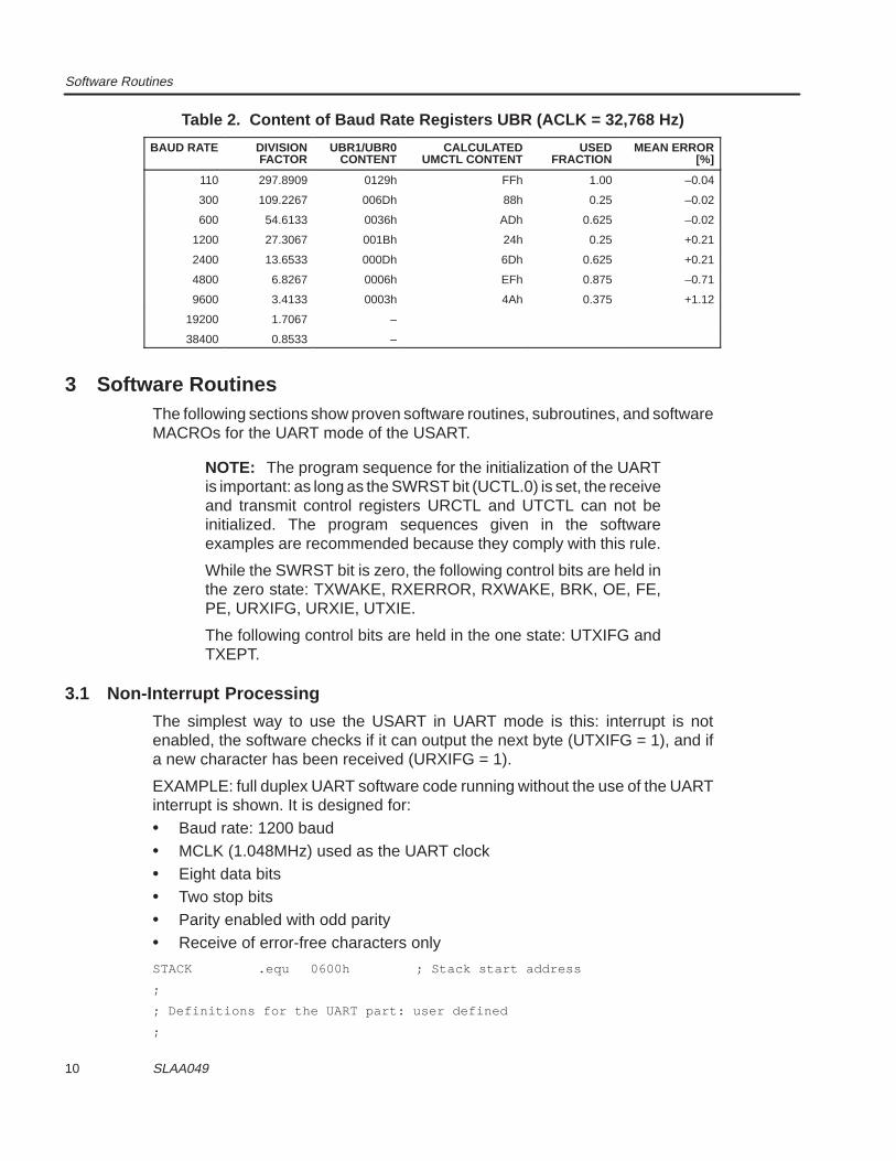
Tables 1 and 2 contain the average errors (full frame) for commonly used baudrates when using the described baud rate generation.
The software examples in section 3 contain MACROs that automatically insertthe correct values in the UBR registers and in the modulation register UMCTL.The software MACROs, which do not need ROM or RAM, may be hidden in thelisting by a .mnolist assembler directive.
2.1 Baud Rate Generation With the MCLKTable 1 shows the optimum values for the UBR and UMCTL registers. The UARTclock is the MCLK (1.048 MHz). The values for the UMCTL and UBR1/UBR0registers are calculated by the software MACROs in section 3.3.2. The crystalerror is not included.

Baud Rate Generation
9 MSP430 Universal Synchronous Asynchronous Receive/Transmit Communication Interface
Table 1 contains the following columns:
• Baud Rate: The baud rate for data exchange (transmit and receive use thesame baud rate).
• Division Factor: The quotient UARTCLK/baud rate.
• UBR1/UBR0 Content: The truncated 16-bit hexadecimal result of thedivision factor (UARTCLK/baud rate). Its value is calculated by softwaremacro CALC_UBR. The high byte is the UBR1 value, the low byte is the UBR0value.
• Calculated UMCTL Content: The 8-bit result that best fits the modulationregister. It is calculated by the software macro CALC_UMCTL.
• Used Fraction: The number of ones in the modulation register divided byeight. It is an approximation to the truncated fractional-part of the divisionfactor.
• Mean Error: The resulting error of a complete character, caused by theapproximation to the division factor.
Table 1. Content of Baud Rate Registers UBR (MCLK = 1.048 MHz)
BAUD RATE DIVISIONFACTOR
UBR1/UBR0CONTENT
CALCULATEDUMCTL CONTENT
USEDFRACTION
MEAN ERROR[%]
110 9532.51 253Ch 55h 0.50 +0.000
300 3495.25 0DA7h 44h 0.25 0.000
600 1747.63 06D3h 6Dh 0.625 +0.000
1200 873.81 0369h EFh 0.875 –0.007
2400 436.91 01B4h FFh 1.00 –0.002
4800 218.45 00DAh AAh 0.50 –0.023
9600 109.23 006Dh 88h 0.25 –0.018
19200 54.61 0036h ADh 0.625 –0.027
38400 27.31 001Bh 24h 0.25 +0.220
2.2 Baud Rate Generation With the ACLK
With the relatively low ACLK frequency (32,768Hz), the importance of themodulation register UMCTL is much greater than with the normally high MCLKfrequency used for the UART timing. Table 2 shows the optimum values for theUBR and UMCTL registers for commonly used baud rates generated with theACLK (32,768Hz). The table values are calculated by the MACROs described insection 3.3.2. The crystal is assumed to have no frequency-error. The meaningof the table columns is explained in section 2.1.
Software Routines
10 SLAA049
Table 2. Content of Baud Rate Registers UBR (ACLK = 32,768 Hz)
BAUD RATE DIVISIONFACTOR
UBR1/UBR0CONTENT
CALCULATEDUMCTL CONTENT
USEDFRACTION
MEAN ERROR[%]
110 297.8909 0129h FFh 1.00 –0.04
300 109.2267 006Dh 88h 0.25 –0.02
600 54.6133 0036h ADh 0.625 –0.02
1200 27.3067 001Bh 24h 0.25 +0.21
2400 13.6533 000Dh 6Dh 0.625 +0.21
4800 6.8267 0006h EFh 0.875 –0.71
9600 3.4133 0003h 4Ah 0.375 +1.12
19200 1.7067 –
38400 0.8533 –
3 Software RoutinesThe following sections show proven software routines, subroutines, and softwareMACROs for the UART mode of the USART.
NOTE: The program sequence for the initialization of the UARTis important: as long as the SWRST bit (UCTL.0) is set, the receiveand transmit control registers URCTL and UTCTL can not beinitialized. The program sequences given in the softwareexamples are recommended because they comply with this rule.
While the SWRST bit is zero, the following control bits are held inthe zero state: TXWAKE, RXERROR, RXWAKE, BRK, OE, FE,PE, URXIFG, URXIE, UTXIE.
The following control bits are held in the one state: UTXIFG andTXEPT.
3.1 Non-Interrupt Processing
The simplest way to use the USART in UART mode is this: interrupt is notenabled, the software checks if it can output the next byte (UTXIFG = 1), and ifa new character has been received (URXIFG = 1).
EXAMPLE: full duplex UART software code running without the use of the UARTinterrupt is shown. It is designed for:• Baud rate: 1200 baud• MCLK (1.048MHz) used as the UART clock• Eight data bits• Two stop bits• Parity enabled with odd parity• Receive of error-free characters only
STACK .equ 0600h ; Stack start address
;
; Definitions for the UART part: user defined
;
Software Routines
11 MSP430 Universal Synchronous Asynchronous Receive/Transmit Communication Interface
Baudr .equ 1200 ; Baud rate is 1200 Baud
FLLMPY .equ 32 ; FLL multiplier for 1,048MHz
UARTCLK .equ FLLMPY*32768 ; MCLK is used for UARTCLK
;
; The contents of the UMCTL and UBR registers are calculated.
; The two software macros do not use RAM or ROM, they only
; define the variables CUMCTL, CUBR1 and CUBR0 for the
; UART registers UMCTL, UBR1 and UBR0.
;
CALC_UMCTL ; Calc. Modulation Reg. content
CALC_UBR ; Calculate UBR1/UBR0 contents
;
.text ; Software start address
;
INIT MOV #STACK,SP ; Initialize Stack Pointer
CALL #INITSR ; Init. FLL and RAM
.. ; Proceed with initialization
;
; Initialize the UART: odd parity, 8 data bits, 2 stop bits
; MCLK for UART clock
;
MOV.B #CUMCTL,&UMCTL ; Modulation Register
MOV.B #CUBR0,&UBR0 ; Baud Rate Register low
MOV.B #CUBR1,&UBR1 ; Baud Rate Register high
BIS.B #URXD+UTXD,&P4SEL ; Select RXD + TXD at Port4
BIS.B #UTXE+URXE,&ME2 ; Enable USART Modules
MOV.B #PENA+SP_+CHAR,&UCTL ; USART Control Register
MOV.B #SSEL1+SSEL0,&UTCTL ; Transmit Control Reg. MCLK
MOV.B #0,&URCTL ; Receive Control Register
... ; Continue with initialization
;
MAINLOOP ... ; Start Mainloop
;
; UART parts within the main loop.
; The software checks these two parts regularly.
; UART Receive part:
; check if a new character is received
; R7 contains the received information.
BIT.B #RXERR,&URCTL ; Error during receive?
JZ L$3 ; No
... ; Error handling
BIC.B #FE+PE+OE+BRK+RXERR,&URCTL ; Clear error flags
JMP L$2 ; Continue in mainloop

Software Routines
12 SLAA049
;
L$3 BIT.B #URXIFG,&IFG2 ; Character received?
JZ L$2 ; No, proceed to mainloop
MOV.B &URXBUF,R7, ; Yes, move character to R7
L$2 ... ; Continue in mainloop
;
; UART Transmit part:
; check if the next character can be transmitted.
; R6 contains information to be transmitted.
;
BIT.B #UTXIFG,&IFG2 ; Transmit buffer empty?
JZ L$1 ; No, wait
MOV.B R6,&UTXBUF ; Empty: move info to TX buffer
MOV.B src,R6 ; Next character to R6
L$1 ... ; Continue with mainloop
BR #MAINLOOP ; End of mainloop
;
; Interrupt Vectors
;.sect ”INITVEC”,0FFFEh ; Reset Vector
.word INIT ; Program Start Address
Only the following two source lines need to be modified if the previous softwareis to be used with the ACLK as the UART clock:
UARTCLK .equ 32768 ; ACLK is used for UARTCLK
;MOV.B #SSEL0,&UTCTL ; Transmit Control Register ACLK
Macros CALC_UMCTL and CALC_UBRAll automatically make any othermodifications necessary.
3.2 Interrupt Processing
This is the normal mode to use the UART. Interrupt is requested if the generalinterrupt enable bit GIE (SR.3) is set, and:• A character is transmitted, and the transmit interrupt is enabled (IE2.1 = 1),
or• A character is received, and the receive interrupt is enabled (IE2.0 = 1)
NOTE: If an error occurred during the reception of a character,the error flags in the receive control register (PE, FE, BRK, andRXERR) must be reset within the UART interrupt handler.Otherwise the set-error flags will block the next interrupt. Thisdoes not apply to the overrun-error flag OE.
3.2.1 MCLK Used as UART Clock
The following example covers the use of the MCLK to generate the UART clockor external frequencies in the MCLK range (500 kHz to 3.8 MHz).

Software Routines
13 MSP430 Universal Synchronous Asynchronous Receive/Transmit Communication Interface
For high baud-rates—higher than 38,400 baud—dedicated CPU registers maybe necessary to lower the interrupt overhead; time for saving and restoring theregister is not required. The software example shown in section 3.2.2 usesdedicated registers.
EXAMPLE: a full-duplex UART software using the two UART interrupts is shown.It is designed for:• Baud rate: 19200 baud• The MCLK (3.144 MHz) used as the UART clock• Seven data bits• One stop bit• Parity enabled with even-parity• Receive of error-free characters only
Transmit Part: the start address xxxx is loaded into pointer TXPOI, and thenumber of characters to be output is loaded into character count TXCNT. Theinterrupt routine outputs the programmed character sequence starting at addressxxxx.
Receive Part: the start address yyyy of a RAM buffer is loaded into pointerRCPOI, and the number of characters to be received is loaded into charactercount RCCNT. The interrupt routine receives the characters and stores them intothe buffer. Only error-free characters are accepted.
STACK .equ 0600h ; Stack start address
;
; Definitions for the UART part
;
Baudr .equ 19200 ; Baud rate is 19200 Baud
FLLMPY .equ 96 ; FLL multiplier for 3,144MHz
UARTCLK .equ FLLMPY*32768 ; MCLK is used for UARTCLK
;
.even ; Word boundary
.bss TXPOI,2 ; Pointer to transmit buffer
.bss RCPOI,2 ; Pointer to receive buffer
.bss TXCNT,1 ; Counter/status for transmit
.bss RCCNT,1 ; Counter/status for receive
;
; The content for the UMCTL and UBR registers are calculated
; The two software macros do not use RAM or ROM
;
CALC_UMCTL ; Calculate Mod. Reg. content
CALC_UBR ; Calculate UBR1/UBR0 contents
;
.text ; Software start address
;
INIT MOV #STACK,SP ; Initialize Stack Pointer

Software Routines
14 SLAA049
CALL #INITSR ; Init. FLL and RAM
... ; Proceed with initialization
;
; Initialize the UART: Even parity, 7 data bits, 1 stop bit
; MCLK for UART clock, only error-free characters to URXBUF
;
MOV.B #CUMCTL,&UMCTL ; Modulation Register
MOV.B #CUBR0,&UBR0 ; Baud Rate Register low
MOV.B #CUBR1,&UBR1 ; Baud Rate Register high
BIS.B #URXD+UTXD,&P4SEL ; Select RXD + TXD at Port4
BIS.B #UTXE+URXE,&ME2 ; Enable USART Modules
MOV.B #PENA+PEV,&UCTL ; USART Control Register
MOV.B #SSEL1+SSEL0,&UTCTL ; Transmit Control Reg. MCLK
MOV.B #0,&URCTL ; Receive Control Register
BIS.B #UTXIE+URXIE,&IE2 ; Enable USART interrupts
CLR.B TXCNT ; Disable transmit
CLR.B RCCNT ; Disable receive
... ; Continue with initialization
EINT ; Enable interrupt
;
MAINLOOP ... ; Start of Mainloop
;
; Preparation for reception of m bytes. The input
; buffer starts at address yyyy
;
TST.B RCCNT ; Data input completed?
JNZ L$1 ; No, wait
MOV #yyyy,RCPOI ; Buffer start address to RCPOI
MOV.B #m,RCCNT ; Number of bytes to RCCNT
L$1 ... ; Continue in mainloop
;
; Stop the reception of data. The currently received character
; is input completely
;
CLR.B RCCNT ; Status to zero
... ; Continue
;
; Preparation for the transmission of n bytes starting at
; address xxxx. Check if last transmit operation
; is really completed.
;
BIT.B #TXEPT,&UTCTL ; Transmit part ready?
JZ L$2 ; No, buffers are not yet empty

Software Routines
15 MSP430 Universal Synchronous Asynchronous Receive/Transmit Communication Interface
;
MOV.B #n–1,TXCNT ; Ready, init. byte count
MOV #xxxx+1,TXPOI ; Init. transmit buffer pointer
MOV.B xxxx,&UTXBUF ; First info byte to TX buffer
L$2 ... ; Continue in background
;
; Stop the transmission of data. The currently sent character
; is transmitted completely
;
CLR.B TXCNT ; Status to zero
...
;
; Interrupt Handlers
; Interrupt handler for the UART Receive part.
;
RCINT TST.B RCCNT ; Reception allowed?
JZ RCRET ; No, status is 0
BIT.B #RXERR,&URCTL ; Error during receive?
JNZ RCERR ; Yes
DEC.B RCCNT ; No, Byte count –1
PUSH R5 ; Save R5
MOV RCPOI,R5 ; Pointer to buffer
MOV.B &URXBUF,0(R5) ; Next byte to buffer
INC R5 ; To next buffer byte
MOV R5,RCPOI ; Update pointer
POP R5 ; Restore R5
RCRET RETI
;
RCERR ... ; Error handling
BIC.B #FE+PE+OE+BRK+RXERR,&URCTL ; Clear error flags
RETI
;
; Interrupt handler for the UART Transmit part.
;
TXINT TST.B TXCNT ; Something to transmit?
JZ TXRET ; No, buffer is empty
DEC.B TXCNT ; Byte count –1
PUSH R5
MOV TXPOI,R5 ; Pointer to buffer
MOV.B @R5+,&UTXBUF ; Next byte for output
MOV R5,TXPOI ; Update pointer
POP R5
TXRET RETI

Software Routines
16 SLAA049
;
; Interrupt Vectors
;
.sect ”SCIVEC”,0FFECh ; USART interrupt vectors
.word TXINT ; Transmit vector
.word RCINT ; Receive vector
.sect ”INITVEC”,0FFFEh ; Reset vector
.word INIT ; Program start address
3.2.2 ACLK Used as UART Clock
The following example deals with the ACLK used to generate the UART clock,or external frequencies lower than 100 kHz. Basically the same method used insection 3.2.1 can be applied to the ACLK used as the UART clock. See section3.2.1 for an explanation.
This section shows a different approach: here the CPU is normally off, and leavesthe LPM3 only when the number of received or transmitted charactersprogrammed is reached.
EXAMPLE: full-duplex UART software code using the UART interrupt is shown.It is designed for:
• Baud rate: 2400 baud
• The ACLK (32,768Hz) used as the UART clock
• Eight data bits
• Two stop bits
• Parity enabled with odd-parity
• Receive of error-free characters only
• The CPU normally uses the low-power mode 3 (LPM3)
Transmit Part: the start address xxxx of the output sequence is loaded intopointer TXPOI, and the number of characters m is loaded into character countTXCNT. The interrupt routine outputs the character sequence and then, whenTXCNT reaches zero (output completed), it resets the CPUoff bit of the storedstatus register on the stack. This manipulation omits the return to LPM3 andallows initialization of the next transmit sequence. R6 is exclusively used for thetransmit part.
Receive Part: the start address yyyy of a RAM buffer is loaded into pointerRCPOI, and the number of characters n is loaded into character count RCCNT.The interrupt routine receives the characters and stores them in the buffer untilRCCNT reaches zero (input completed). Then it resets the CPUoff bit of thestored status register on the stack. This manipulation omits the return to LPM3and allows to process the received data. Only error-free characters are accepted.R7 is exclusively used for the receive part.

Software Routines
17 MSP430 Universal Synchronous Asynchronous Receive/Transmit Communication Interface
STACK .equ 0600h ; Stack start address
;
; Definitions for the UART part
;
Baudr .equ 2400 ; Baud rate is 2400 Baud
FLLMPY .equ 64 ; FLL multiplier for 2,096MHz
UARTCLK .equ 32768 ; ACLK is used for UARTCLK
;
.bss TXCNT,1 ; Counter/status for transmit
.bss RCCNT,1 ; Counter/status for receive
CALC_UMCTL ; Calculate Mod. Reg. content
CALC_UBR ; Calculate UBR1/UBR0 contents
;
.text ; Software start address
;
INIT MOV #STACK,SP ; Initialize Stack Pointer
CALL #INITSR ; Init. FLL and RAM
... ; Proceed with initialization
;
; Initialize the UART: Odd parity, 8 data bits, 2 stop bits
; ACLK used for the UART clock
;MOV.B #CUMCTL,&UMCTL ; Modulation Register
MOV.B #CUBR0,&UBR0 ; Baud rate register low
MOV.B #CUBR1,&UBR1 ; Baud rate register high
BIS.B #URXD+UTXD,&P4SEL ; Select RXD + TXD at Port4
BIS.B #UTXE+URXE,&ME2 ; Enable USART modules
MOV.B #PENA+SP_+CHAR,&UCTL ; USART control register
MOV.B #SSEL0,&UTCTL ; Transmit contr. reg. ACLK
MOV.B #0,&URCTL ; Receive control register
BIS.B #UTXIE+URXIE,&IE2 ; Enable USART interrupts
CLR.B TXCNT ; Disable transmit
CLR.B RCCNT ; Disable receive
... ; Continue with initialization
EINT ; Enable interrupt (GIE = 1)
;
MAINLOOP ... ; Start Mainloop
;
; Preparation for the reception of m bytes. Buffer starts
; at address yyyy. R7 is a dedicated register for receive
;
TST.B RCCNT ; Ready?
JNZ L$1 ; No, RCCNT > 0

Software Routines
18 SLAA049
MOV #yyyy,R7 ; Receive buffer start address
MOV.B #m,RCCNT ; Number of bytes
L$1 ...
;
; Stop the reception of data. The actually received character
; is input completely
;
CLR.B RCCNT ; Status is zero
...
;
; Preparation for transmission of n bytes starting at
; address xxxx. R6 is a dedicated register for transmit.
; The check for the empty TX buffer is faster, but needs more
; ROM bytes.
;TST.B TXCNT ; Ready for next characters?
JNZ L$2 ; No, TXCNT > 0
BIT.B #UTXIFG,&IFG2 ; TX part also ready?
JZ L$2 ; No, busy
;
MOV.B #n–1,TXCNT ; Ready, init. byte count
MOV #xxxx+1,R6 ; Init. transmit buffer pointer
MOV.B xxxx,&UTXBUF ; First info byte to TX buffer
L$2 ... ; Continue in background
;
; Stop transmission of data. The actually sent character
; is transmitted completely
;CLR.B TXCNT ; Status is zero
...
;
; After completion of all tasks, the program enters LPM3
;
PLPM3 BIS #CPUoff+GIE+SCG1+SCG0,SR ; Enter LPM3
;
; An interrupt handler cleared the CPUoff bit on the stack.
; Checks are made to see if activity is needed:
: Receive: receive input buffer full
; Transmit: transmit buffer output completely
; ... other interrupt handlers
;TST.B RCCNT ; Receive completed?
JZ PROCRC ; Yes, process received data
TST.B TXCNT ; Transmit completed?

Software Routines
19 MSP430 Universal Synchronous Asynchronous Receive/Transmit Communication Interface
JZ NXTTX ; Yes, prepare next characters
... ; Other handlers?
JMP PLPM3 ; Back to LPM3
;
; Interrupt Handlers
; Interrupt handler for the UART Receive part. R7 is used
; only for the receive part.
;
RCINT TST.B RCCNT ; Reception allowed?
JZ RCRET ; No, status is 0
BIT.B #RXERR,&URCTL ; Error during receive?
JNZ RCERR ; Yes
DEC.B RCCNT ; Byte count –1
MOV.B &URXBUF,0(R7) ; Next byte to buffer
INC R7 ; To next buffer byte
TST.B RCCNT ; Buffer filled?
JNZ RCRET ; No, proceed
BIC #CPUoff+SCI1+SCI0,0(SP) ; Active Mode after RETI
RCRET RETI
;
RCERR ... ; Error handling
BIC.B #FE+PE+OE+BRK+RXERR,&URCTL; Clear error flags
RETI
;
; Interrupt handler for the UART Transmit part. R6 is used
; only for the transmit part
;
TXINT TST.B TXCNT ; Something to transmit?
JZ TXRET ; No, buffer is empty
DEC.B TXCNT ; Byte count –1
MOV.B @R6+,&UTXBUF ; Next byte for output
TST.B TXCNT ; Buffer output?
JNZ TXRET ; No, proceed
BIC #CPUoff+SCI1+SCI0,0(SP) ; Active Mode after RETI
TXRET RETI
;
; Interrupt vectors
;
sect ”SCIVEC”,0FFECh ; USART Interrupt vectors
word TXINT ; Transmit vector
word RCINT ; Receive vector
sect ”INITVEC”,0FFFEh ; Reset vector
word INIT ; Program start address
Software Routines
20 SLAA049
3.3 Subroutines and .MACROs
This section contains the subroutines and assembler .MACROs used in theprevious examples.
3.3.1 Subroutines
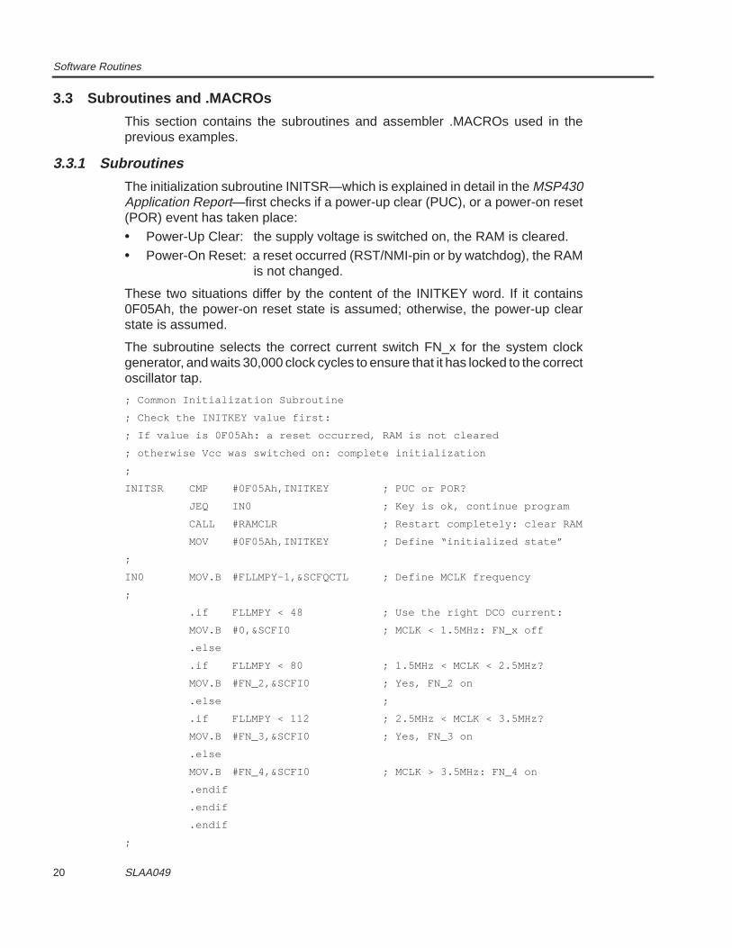
The initialization subroutine INITSR—which is explained in detail in the MSP430Application Report—first checks if a power-up clear (PUC), or a power-on reset(POR) event has taken place:• Power-Up Clear: the supply voltage is switched on, the RAM is cleared.• Power-On Reset: a reset occurred (RST/NMI-pin or by watchdog), the RAM
is not changed.
These two situations differ by the content of the INITKEY word. If it contains0F05Ah, the power-on reset state is assumed; otherwise, the power-up clearstate is assumed.
The subroutine selects the correct current switch FN_x for the system clockgenerator, and waits 30,000 clock cycles to ensure that it has locked to the correctoscillator tap.
; Common Initialization Subroutine
; Check the INITKEY value first:
; If value is 0F05Ah: a reset occurred, RAM is not cleared
; otherwise Vcc was switched on: complete initialization
;
INITSR CMP #0F05Ah,INITKEY ; PUC or POR?
JEQ IN0 ; Key is ok, continue program
CALL #RAMCLR ; Restart completely: clear RAM
MOV #0F05Ah,INITKEY ; Define “initialized state”
;
IN0 MOV.B #FLLMPY–1,&SCFQCTL ; Define MCLK frequency
;
.if FLLMPY < 48 ; Use the right DCO current:
MOV.B #0,&SCFI0 ; MCLK < 1.5MHz: FN_x off
.else
.if FLLMPY < 80 ; 1.5MHz < MCLK < 2.5MHz?
MOV.B #FN_2,&SCFI0 ; Yes, FN_2 on
.else ;
.if FLLMPY < 112 ; 2.5MHz < MCLK < 3.5MHz?
MOV.B #FN_3,&SCFI0 ; Yes, FN_3 on
.else
MOV.B #FN_4,&SCFI0 ; MCLK > 3.5MHz: FN_4 on
.endif
.endif
.endif
;

Software Routines
21 MSP430 Universal Synchronous Asynchronous Receive/Transmit Communication Interface
MOV #10000,R5 ; Allow the FLL to settle
IN1 DEC R5 ; at the correct DCO tap
JNZ IN1 ; during 30000 cycles
RET ; Return from initialization
;
; Subroutine for clearing of the RAM block
;
.bss INITKEY,2,0200h ; 0F05Ah: initialized state
RAMSTRT .equ 0200h ; Start of RAM
RAMEND .equ 05FEh ; Highest RAM address (33x)
;
RAMCLR CLR R5 ; Prepare index register
RCL CLR RAMSTRT(R5) ; 1st RAM address
INCD R5 ; Next word address
CMP #RAMEND–RAMSTRT+2,R5 ; RAM cleared?
JLO RCL ; No, once more
RET ; Yes, return
3.3.2 .MACROs
The two following software macros calculate the best-fit values of the UARTbaud-rate generator. They do not use ROM or RAM, and they define the threevariables, CUBR1, CUBR0, and CUMCTL, used during initialization of UARTregisters UBR1, UBR0, and UMCTL.
.mnolist ; Do not list macro calls
;
; The values for the modulation registers UBR1/UBR0 are
; calculated: CUBR1 and CUBR0 contain the truncated result
; of the UARTCLK/Baudr division.
;
CALC_UBR .macro
CUBR1 .equ UARTCLK/(Baudr*256) ; Baud Rate Reg. High
CUBR0 .equ (UARTCLK/Baudr)–256*CUBR1 ; Baud Rate Reg. Low
.endm
The calculation of the modulation register UMCTL content follows. Seven bits ofresolution are used.
CALC_UMCTL .macro
;; Modulation Register content: the rounded fraction of
; CMOD = UARTCLK/Baudr is calculated
; Binary format of CMOD: 0.xxxxxxx
; Then the 8 bits of UMCTL are built.
; Inputs: UARTCLK, Baudr ; Frequencies [Hz]
; Output: CUMCTL ; 8–bit UMCTL register value;
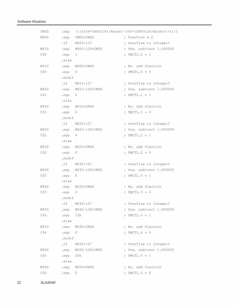
Software Routines
22 SLAA049
CMOD .equ ((((256*UARTCLK)/Baudr)–256*(UARTCLK/Baudr))+1)/2
M$00 .equ CMOD+CMOD ; Fraction x 2
.if M$00>127 ; Overflow to integer?
M$10 .equ M$00–128+CMOD ; Yes, subtract 1.000000
C$0 .equ 1 ; UMCTL.0 = 1
.else
M$10 .equ M$00+CMOD ; No, add fraction
C$0 .equ 0 ; UMCTL.0 = 0
.endif
.if M$10>127 ; Overflow to integer?
M$20 .equ M$10–128+CMOD ; Yes, subtract 1.000000
C$1 .equ 2 ; UMCTL.1 = 1
.else
M$20 .equ M$10+CMOD ; No, add fraction
C$1 .equ 0 ; UMCTL.1 = 0
.endif
.if M$20>127 ; Overflow to integer?
M$30 .equ M$20–128+CMOD ; Yes, subtract 1.000000
C$2 .equ 4 ; UMCTL.2 = 1
.else
M$30 .equ M$20+CMOD ; No, add fraction
C$2 .equ 0 ; UMCTL.2 = 0
.endif
.if M$30>127 ; Overflow to integer?
M$40 .equ M$30–128+CMOD ; Yes, subtract 1.000000
C$3 .equ 8 ; UMCTL.3 = 1
.else
M$40 .equ M$30+CMOD ; No, add fraction
C$3 .equ 0 ; UMCTL.3 = 0
.endif
.if M$40>127 ; Overflow to integer?
M$50 .equ M$40–128+CMOD ; Yes, subtract 1.000000
C$4 .equ 10h ; UMCTL.4 = 1
.else
M$50 .equ M$40+CMOD ; No, add fraction
C$4 .equ 0 ; UMCTL.4 = 0
.endif
.if M$50>127 ; Overflow to integer?
M$60 .equ M$50–128+CMOD ; Yes, subtract 1.000000
C$5 .equ 20h ; UMCTL.5 = 1
.else
M$60 .equ M$50+CMOD ; No, add fraction
C$5 .equ 0 ; UMCTL.5 = 0
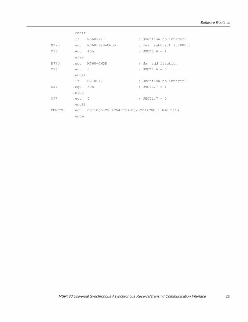
Software Routines
23 MSP430 Universal Synchronous Asynchronous Receive/Transmit Communication Interface
.endif
.if M$60>127 ; Overflow to integer?
M$70 .equ M$60–128+CMOD ; Yes, subtract 1.000000
C$6 .equ 40h ; UMCTL.6 = 1
.else
M$70 .equ M$60+CMOD ; No, add fraction
C$6 .equ 0 ; UMCTL.6 = 0
.endif
.if M$70>127 ; Overflow to integer?
C$7 .equ 80h ; UMCTL.7 = 1
.else
C$7 .equ 0 ; UMCTL.7 = 0
.endif
CUMCTL .equ C$7+C$6+C$5+C$4+C$3+C$2+C$1+C$0 ; Add bits
.endm
References
24 SLAA049
4 References1. MSP430 Family Architecture Guide and Module Library, 1996, Literature No.
SLAUE10B
2. MSP430 Application Report, 1998, Literature No. SLAAE10C
3. Data Sheet MSP430x33x, 1998, Literature No. SLAS163
Definitions
A-1 MSP430 Universal Synchronous Asynchronous Receive/Transmit Communication Interface
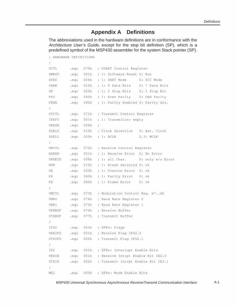
Appendix A DefinitionsThe abbreviations used in the hardware definitions are in conformance with theArchitecture User’s Guide, except for the stop bit definition (SP), which is apredefined symbol of the MSP430 assembler for the system Stack pointer (SP).
; HARDWARE DEFINITIONS
;
UCTL .equ 070h ; USART Control Register
SWRST .equ 001h ; 1: Software Reset 0: Run
SYNC .equ 004h ; 1: UART Mode 0: SCI Mode
CHAR .equ 010h ; 1: 8 Data Bits 0: 7 Data Bits
SP .equ 020h ; 1: 2 Stop Bits 0: 1 Stop Bit
PEV .equ 040h ; 1: Even Parity 0: Odd Parity
PENA .equ 080h ; 1: Parity enabled 0: Parity dis.
;
UTCTL .equ 071h ; Transmit Control Register
TXEPT .equ 001h ; 1: Transmitter empty
URXSE .equ 008h ;
SSEL0 .equ 010h ; Clock Selection 0: Ext. Clock
SSEL1 .equ 020h ; 1: ACLK 2,3: MCLK
;
URCTL .equ 072h ; Receive Control Register
RXERR .equ 001h ; 1: Receive Error 0: No Error
URXEIE .equ 008h ; 1: all Char. 0: only w/o Error
BRK .equ 010h ; 1: Break detected 0: ok
OE .equ 020h ; 1: Overrun Error 0: ok
PE .equ 040h ; 1: Parity Error 0: ok
FE .equ 080h ; 1: Frame Error 0: ok
;
UMCTL .equ 073h ; Modulation Control Reg. m7..m0
UBR0 .equ 074h ; Baud Rate Register 0
UBR1 .equ 075h ; Baud Rate Register 1
URXBUF .equ 076h ; Receive Buffer
UTXBUF .equ 077h ; Transmit Buffer
;
IFG2 .equ 003h ; SFRs: Flags
URXIFG .equ 001h ; Receive Flag IFG2.0
UTXIFG .equ 002h ; Transmit Flag IFG2.1
;
IE2 .equ 001h ; SFRs: Interrupt Enable Bits
URXIE .equ 001h ; Receive Intrpt Enable Bit IE2.0
UTXIE .equ 002h ; Transmit Intrpt Enable Bit IE2.1
;
ME2 .equ 005h ; SFRs: Mode Enable Bits
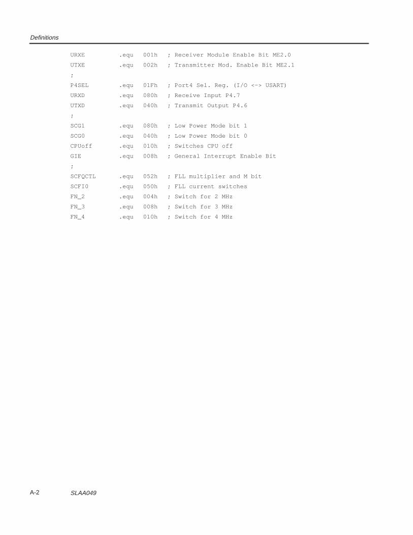
Definitions
A-2 SLAA049
URXE .equ 001h ; Receiver Module Enable Bit ME2.0
UTXE .equ 002h ; Transmitter Mod. Enable Bit ME2.1
;
P4SEL .equ 01Fh ; Port4 Sel. Reg. (I/O <–> USART)
URXD .equ 080h ; Receive Input P4.7
UTXD .equ 040h ; Transmit Output P4.6
;
SCG1 .equ 080h ; Low Power Mode bit 1
SCG0 .equ 040h ; Low Power Mode bit 0
CPUoff .equ 010h ; Switches CPU off
GIE .equ 008h ; General Interrupt Enable Bit
;
SCFQCTL .equ 052h ; FLL multiplier and M bit
SCFI0 .equ 050h ; FLL current switches
FN_2 .equ 004h ; Switch for 2 MHz
FN_3 .equ 008h ; Switch for 3 MHz
FN_4 .equ 010h ; Switch for 4 MHz


