Date post: | 18-Dec-2015 |
Category: |
Documents |
View: | 227 times |
Download: | 0 times |
2- 1
ARM966E-Mem-JTAG-Clock
MS_uC / dnd / V08
Programming MicrocontrollerARM966E-S specifications: Memory – JTAG - Clock
Autumn term 2007
32K Byte 32K Byte Burst FlashBurst Flash
64K or 96K 64K or 96K Byte SRAM Byte SRAM
256K or 512K 256K or 512K Byte Burst Byte Burst
FlashFlash
OTP OTP MemMem
UARTUARTI2CI2CSPISPITIMTIMRTCRTC
EXT. EXT. Bus Bus
GPIOGPIO
USB USB 2.0FS 2.0FS
CAN CAN 2.0B 2.0B
Enet Enet MAC MAC
PFPFQ Q
BC BC
DMADMA
INTINTR R
CntlCntl
ARM96ARM966E 6E CORE CORE
w/DSPw/DSP96 MHz 96 MHz
CLK CLK CntlCntl
ADCADC
LVD LVD BODBOD
PLLPLL JTAJTAGG
ETMETM99
2- 2
ARM966E-Mem-JTAG-Clock
MS_uC / dnd / V08
ARM966E Benefits vs. ARM7TDMI:Harvard / von Neumann Architecture
5 stage pipeline reduces Clocks Per Instruction (CPI)
PIPELINE
CPUCORE
PIPELINE
CPUCORE
ARM966E
ARM7TDMI
AHB/APB
BUS/APB
F = Fetch
D = Decode
E = Execute
M = Memory Read
W = Memory Write-Back
Harvard Architecture improves Load/Store performance
ARMv5TE Architecture with DSP Instructions (1-cycle 32x16 MAC, Saturated Math, and others)
Tightly Coupled Memories (TCM), more deterministic
AHB and DTCM Write Buffers for less stalls
F D E M W
F D E M W
F D E M W
F D E M W
F D E M W
F D E M
F D E
F D
F
5-STAGE PIPELINE
CPUCORE
F D E F D
F D E F D
F D E F D
E F D E
E F D
E F
3-STAGE PIPELINE
CPUCORE
ARM966E
ARM7TDMI
AHB/APB
BUS/APB
F D E M W
F D E M W
F D E M W
F D E M W
F D E M W
F D E M
F D E
F D
F
CODE5-STAGE PIPELINE
CPUCORE
CODEMEMORY
DATAMEMORY
F D E F D
F D E F D
F D E F D
E F D E
E F D
E F
3-STAGE PIPELINE
CPUCORE
CODE ANDDATA
MEMORYCOMBINED
ARM966E
ARM7TDMI
Harvard Architecture
Von Neumann Architecture
CODE & DATA
DATA
AHB/APB
BUS/APB
F D E M W
F D E M W
F D E M W
F D E M W
F D E M W
F D E M
F D E
F D
F
I-TCM
D-TCM
CODE5-STAGE PIPELINE
CPUCORE
CODEMEMORY
WRITEBUFFER
DATAMEMORY
F D E F D
F D E F D
F D E F D
E F D E
E F D
E F
3-STAGE PIPELINE
CPUCORE
CODE ANDDATA
MEMORYCOMBINED
ARM966E
ARM7TDMI
Harvard Architecture
Von Neumann Architecture
CODE & DATA
DATA
AHB/APB
BUS/APB
®
2- 3
ARM966E-Mem-JTAG-Clock
MS_uC / dnd / V08
What, an ARM9 with no Cache?
STR910 is taking a unique approach to Eliminate the need for Traditional Cache memory, but at the same time…
Keep performance high while executing code directly from Flash memory
Keep interrupt latency low with less jitter
Keep device cost to a minimum
Maintain a single-chip embedded control system
Traditional Instruction Cache memory is not good for real-time embedded control
Interrupt Response Time has a lot of “jitter”
Traditional Cache Memory requires lots of Silicon area …. More Expensive
Some Traditional Cache memory systems rely on external memory devices (Flash, SDRAM)
®
2- 4
ARM966E-Mem-JTAG-Clock
MS_uC / dnd / V08
F D E M W
F D E M W
F D E M W
F D E M W
F D E M W
F D E M
F D E
F D
F
I-TCM
D-TCM
CODE5-STAGE PIPELINE
CPUCORE
CODEMEMORY
WRITEBUFFER
DATAMEMORY
ARM966E
DATA
AHB/APB BASIC CORE ARCHITECTURE
STR910 Enhancements of ARM966E
32-bit wide Single-Cycle SRAM
32-bit wide Burst Flash Memory
Burst Memory interface Operates up to 96MHz (10.4 ns) when retrieving Sequential 1-Word Instructions
F D E M W
F D E M W
F D E M W
F D E M W
F D E M W
F D E M
F D E
F D
F
I-TCM
D-TCM
CODE5-STAGE PIPELINE
CPUCORE
BURSTI/F
WRITEBUFFER
ARM966E
DATA
AHB/APB
32-bit wideBurst Flash(to 544KB)
32-bit wideSRAM
(to 96KB)
F D E M W
F D E M W
F D E M W
F D E M W
F D E M W
F D E M
F D E
F D
F
I-TCM
D-TCM
CODEPFQ /
BC
5-STAGE PIPELINE
CPUCORE
BURSTI/F
WRITEBUFFER
ARM966E
DATA
AHB/APB
32-bit wideBurst Flash(to 544KB)
32-bit wideSRAM
(to 96KB)
Pre-Fetch Queue (PFQ) and Branch Cache (BC) PFQ always looks ahead fetching instructions during idle bus
cycles BC remembers last four jumps, immediately loading PFQ
upon jump (branch)
®
2- 5
ARM966E-Mem-JTAG-Clock
MS_uC / dnd / V08
Pre-Fetch Queue and Branch Cache
BC holds 4 instructions for each of 4 most recent branches
BC loads PFQ immediately with all 4 instructions at once into PFQ if branch address matches
PFQ will not stall upon a branch match
5th BC entry has instructions to read VIC
PFQ will not flush when CPU reads a literal (a constant in instruction memory)
What happens
when instructions
are not sequential?
Will PFQ stall?
What happens
when instructions
are not sequential?
Will PFQ stall?
IRQHANDLER
READVIC
READVIC
READVIC
READVIC
ARM966ECPU
BURSTFLASH
MEMORY32 wide32 wide
4 Words of Instruction(programmable depth to 8)
Pre-Fetch Queue (PFQ)
COMPARE
CURRENTBRANCH
ADDRESS
PREVIOUSBRANCH 4
ADDR
INST4A
INST4D
INST4C
INST4B
PREVIOUSBRANCH 3
ADDR
INST3A
INST3D
INST3C
INST3B
PREVIOUSBRANCH 2
ADDR
INST2A
INST2D
INST2C
INST2B
LOAD IF BRANCH MATCH
BranchCache(BC)
INST1D
PREVIOUSBRANCH 1ADDRESS
INST1A
INST1C
INST1B
®
2- 6
ARM966E-Mem-JTAG-Clock
MS_uC / dnd / V08
JTAG Specifics
JTAG Interface 5 standard signals (JTDI, JTDO,
JTMS, JTCK, JTAG) complying with IEEE-1149.1 specification
Additional JRTCK (return TCK) Not required if ARM core
clock 10 times JTCK Required to pace JTCK if ARM
core clock less than 10 times JTCK
In-System Programming Program and erase Main and
Second Flash through JTAG Program OTP Configure STR91xF with software
configuration to
Boundary Scan All pins except JTAG, Oscillator
Inputs and TAMPER_IN
JTAG Debug using ARM EmbeddedICE-RT logic Halt or Monitor mode 2 breakpoints/watchpoints, run,
halt, single step
JTAG Security Bit When set disables all JTAG
operations except ‘Full Chip Erase’
JTAG: Joint Test Action GroupIEEE 1149.1-1990: Standard Test Access Port and Boundary-Scan Architecture
®
2- 7
ARM966E-Mem-JTAG-Clock
MS_uC / dnd / V08
ETM: Enhanced trace module Specifics
Embedded ETM9 adds additional debug capability Real-time instruction flow
Trace Trace filtering and
triggering
ETM Connector
ETM9 Module
ARM996ESCore
JTAG Debug TAP
USB to ETM Trace
Port Analyzer
IARSignum
US
B
Compressed Trace Stream
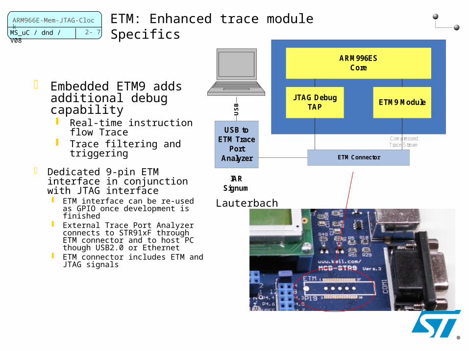
Dedicated 9-pin ETM interface in conjunction with JTAG interface ETM interface can be re-used as
GPIO once development is finished
External Trace Port Analyzer connects to STR91xF through ETM connector and to host PC though USB2.0 or Ethernet
ETM connector includes ETM and JTAG signals
Lauterbach
®
2- 8
ARM966E-Mem-JTAG-Clock
MS_uC / dnd / V08STR910 Memory Map
Single Linear Address Range 4 Gigabyte range Harvard busses transparent to
firmware Code and data separated in silicon
High Speed Peripherals on AHB
Lower Speed Peripherals on APB Firmware accesses APB through
a bridge, or window, on the AHB
Separate Ranges for Write Buffer Peripherals have two address ranges One for buffered writes and another
for non-buffered writes Buffered writes increase overall
performance Non-buffered writes guarantee data
coherency
Dual Flash Bank Memories MCU can write/erase one while
reading other Either Flash can reside at boot
location (address 0x00000000) Bank order is user defined
®0x0000.0000
VICs
PRIMARYFLASH BANK
SECONDARYFLASH BANK
PRIMARYFLASH BANK
SECONDARYFLASH BANK
ORDER OF BANKS IS USER DEFINED
0xFFFF.FFFF
I-TCM(Flash)
D-TCM(SRAM)
AHBBUFFERED
WRITES
AHB NON-BUFFERED
WRITES
APBPERIPHERALS
NON-BUFFEREDWRITES
APB BRIDGE
BUFFERED WRITESAPB BRIDGE
2- 9
ARM966E-Mem-JTAG-Clock
MS_uC / dnd / V08
Flexible Clock Management
Master Clock Control selectable from three sources Main Oscillator RTC Clock PLL
From the master clock the CCU generates individually gated and scaled clock sources for CPU fCPUCLK AHB fAHBCLK EMI fEMICLK UART Baud Generators fBAUD Standard Timerss fTIM01 and fTIM23 USB fUSB
USB Interface Clock comes from one of three sources fMSTR at 48MHz fMSTR at 96MHz with optional divide-by-two External 48 MHz on pin P2.7
Ethernet MAC Clock comes from one of two sources 25 MHz from Main Oscillator (fOSC) output from P5.2 External 25MHz connected to external PHY.
®
2- 10
ARM966E-Mem-JTAG-Clock
MS_uC / dnd / V08
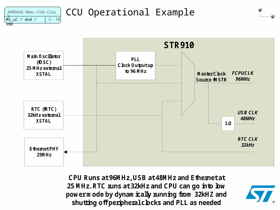
CCU Operational Example
STR910Main Oscillator
(fOSC)25 MHz external
XSTAL
RTC (fRTC)32kHz external
XSTAL
PLLClock Output up
to 96 MHz Master Clock Source fMSTR
1/2
FCPUCLK 96MHz
USB CLK 48MHz
Ethernet PHY 25MHz
RTC CLK 32kHz
CPU Runs at 96MHz, USB at 48MHz and Ethernet at 25 MHz. RTC runs at 32kHz and CPU can go into low power mode by dynamically running from 32kHZ and
shutting off peripheral clocks and PLL as needed ®
2- 11
ARM966E-Mem-JTAG-Clock
MS_uC / dnd / V08
Clock Control Unit (CCU)
STR910
Main Oscillator
(fOSC)
RTC (fRTC)32kHz
PLL
Ethernet PHY
Divider 1,2, 4, 8 16, 1024
AHB (1,2,4)
Clock Peripheral
Control
APB (1,2,4,8)
Clock Peripheral
Control
Clock Peripheral
Control
Clock Peripheral
Control
1/2
1/2
16-bit prescaler
16-bit prescaler
16-bit prescaler
Clock Peripheral
Control
Clock Peripheral
Control
Clock Peripheral
Control
Clock Peripheral
Control
1/2
External Clock
USB in 48MHz
48MHz
Master Clock
AHB Periph Clock
APB Periph Clock
CPU & PFQC Clock
FMI Clock
Baud Rate Clock
Motor Control Clock
EFT1&2 Clock
EFT3&4 Clock
USB Clock
®
UART, ...
GPIO 7
Examples: