2017 Microchip Technology Inc. DS60001524A-page 1 Description ATSENSE-101/ATSENSE-201(H)/ATSENSE-301(H) are multi-channel analog front end devices which integrate three, four or seven simultaneously sampled Sigma-Delta A/D converters, a high-precision voltage reference with up to 10 ppm/°C temperature stability (H-versions), a programmable current signal amplification, a temperature sensor and an SPI interface. When used in data acquisition and energy measurement applications in combination with the Microchip ATSAM4C device family that features a dedicated Cortex ® -M4 processor and metrology library and a variety of sensors including Shunt, CT and Rogowski coils, the ATSENSE-101/ATSENSE-201(H)/ATSENSE-301(H) exceeds ANSI C12.20-2002 and IEC 62053-22 metering accuracy classes of up to 0.2% over 3000:1 current range. Features • Analog Front End - Single-phase (ATSENSE-101), Dual-phase (ATSENSE-201(H)) or Poly-phase (ATSENSE-301(H)) Energy Metering Analog Front End Suitable for Microchip MCUs and Metrology Library - Compliant with Class 0.2 Standards (ANSI C12.20-2002 and IEC 62053-22) - Three, Four or Seven Sigma-Delta ADC Measurement Channels: One, Two or Three Voltages, Two or Four Cur- rents, 102 dB Dynamic Range - Current Channels with Pre-Gain (x1, x2, x4, x8) - Supports Shunt, Current Transformer and Rogowski Coils - Dedicated Current Channel for Anti-tamper Measurement - Integrated SINC Decimation Filters. Output Data Rate: 16 kSps typical - Integrated 2.8V LDO Regulator to Supply Analog Functions - 3.0V to 3.6V Operation, Ultra Low Power: < 2.5 mW typical/Channel @ 3.3V - Specified over two ambient operating temperature ranges : [-40°C ; +85°C] and [-40°C;+105°C] • Precision Voltage Reference - Standard 1.2V Output Voltage with Possible External Bypass - Temperature Drift: 50 ppm typical (ATSENSE-101/ATSENSE-201/ATSENSE-301) - Temperature Drift: 10 ppm typical (ATSENSE-201H/ATSENSE-301H) - Factory-measured Temperature Drift and Die Temperature Sensor to Perform Software Correction - Digital Interface - 8 MHz Serial Peripheral Interface (SPI) Compatible Mode 1 (8-bit) for ADC Data and AFE Controls - Interrupt Output Line Signaling ADC End-of-Conversion, Underrun and Overrun • Package - 32-lead TQFP, 7 x 7 x 1.4 mm - 20-lead SOIC, 12.8 x 7.5 x 2.3 mm Multi-Channel Sigma-Delta Analog Front End ATSENSE-101/ATSENSE-201(H)/ ATSENSE-301(H)
Transcript
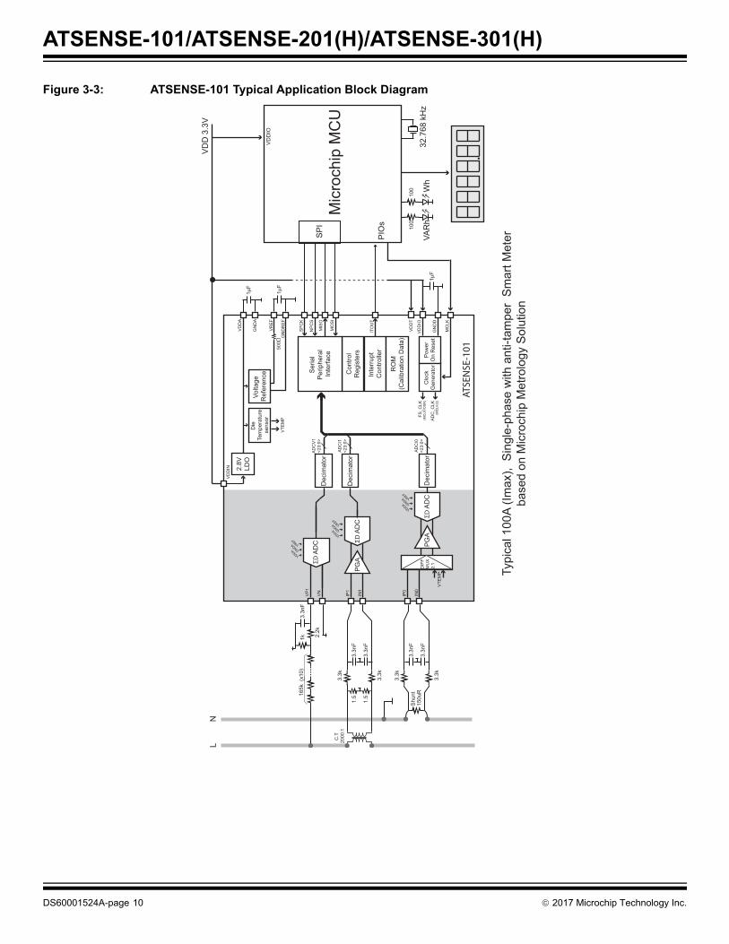
Multi-Channel Sigma-Delta Analog Front End
ATSENSE-101/ATSENSE-201(H)/ATSENSE-301(H)
Description
ATSENSE-101/ATSENSE-201(H)/ATSENSE-301(H) are multi-channel analog front end devices which integrate three,four or seven simultaneously sampled Sigma-Delta A/D converters, a high-precision voltage reference with up to 10ppm/°C temperature stability (H-versions), a programmable current signal amplification, a temperature sensor and anSPI interface. When used in data acquisition and energy measurement applications in combination with the MicrochipATSAM4C device family that features a dedicated Cortex®-M4 processor and metrology library and a variety of sensorsincluding Shunt, CT and Rogowski coils, the ATSENSE-101/ATSENSE-201(H)/ATSENSE-301(H) exceeds ANSIC12.20-2002 and IEC 62053-22 metering accuracy classes of up to 0.2% over 3000:1 current range.
Features
• Analog Front End- Single-phase (ATSENSE-101), Dual-phase (ATSENSE-201(H)) or Poly-phase (ATSENSE-301(H)) Energy
Metering Analog Front End Suitable for Microchip MCUs and Metrology Library- Compliant with Class 0.2 Standards (ANSI C12.20-2002 and IEC 62053-22)- Three, Four or Seven Sigma-Delta ADC Measurement Channels: One, Two or Three Voltages, Two or Four Cur-
rents, 102 dB Dynamic Range- Current Channels with Pre-Gain (x1, x2, x4, x8)- Supports Shunt, Current Transformer and Rogowski Coils- Dedicated Current Channel for Anti-tamper Measurement- Integrated SINC Decimation Filters. Output Data Rate: 16 kSps typical- Integrated 2.8V LDO Regulator to Supply Analog Functions- 3.0V to 3.6V Operation, Ultra Low Power: < 2.5 mW typical/Channel @ 3.3V- Specified over two ambient operating temperature ranges : [-40°C ; +85°C] and [-40°C;+105°C]
• Precision Voltage Reference - Standard 1.2V Output Voltage with Possible External Bypass- Temperature Drift: 50 ppm typical (ATSENSE-101/ATSENSE-201/ATSENSE-301) - Temperature Drift: 10 ppm typical (ATSENSE-201H/ATSENSE-301H) - Factory-measured Temperature Drift and Die Temperature Sensor to Perform Software Correction- Digital Interface- 8 MHz Serial Peripheral Interface (SPI) Compatible Mode 1 (8-bit) for ADC Data and AFE Controls- Interrupt Output Line Signaling ADC End-of-Conversion, Underrun and Overrun
• Package - 32-lead TQFP, 7 x 7 x 1.4 mm- 20-lead SOIC, 12.8 x 7.5 x 2.3 mm
VP3(1) Input 1 Analog Voltage channel 3, positive input
VP2 Input 2 Analog Voltage channel 2, positive input
VP1 Input 3 Analog Voltage channel 1, positive input
VN Input 4 Analog Voltage channels negative input
VREF In / Out 5 Analog Voltage reference output and ADCs reference buffer input
GNDREF Ground 6 Ground Voltage reference ground pin
GNDA Ground 7 GroundGround pin for low noise analog circuits and low noisenegative ADC reference
VDDA In / Out 8 Analog 2.8V LDO output and analog circuits power supply input
IN3(1) Input 9 Analog Current channel 3, negative input
IP3(1) Input 10 Analog Current channel 3, positive input
IN2(1) Input 11 Analog Current channel 2, negative input
IP2(1) Input 12 Analog Current channel 2, positive input
IN1 Input 13 Analog Current channel 1, negative input
IP1 Input 14 Analog Current channel 1, positive input
IN0 Input 15 Analog Current channel 0 (Tamper), negative input
IP0 Input 16 Analog Current channel 0 (Tamper), positive input
- - 17 .. 22 - Not connected. Connect to ground
VDDIO Input 23 PowerPower supply input pin for digital I/O and digital corecircuits
GNDD Ground 24 Ground Ground pin for digital I/O and digital core circuits
1
VP
3
2
VP
2
3
VP
1
4V
N5
VR
EF
6
GN
DR
EF
7
GN
DA
8
VD
DA
9IN3
10IP3
11IN2
12IP2
13IN1
14IP1
15IN0
16IP0
32 VDDIN
31 VDDT
30 MCLK
29 NPCS
28 MISO
27 MOSI
26 SPCK
25 ITOUT
24 23 22 21 20 19 18 17
GN
DD
VD
DIO
- - - - - -
ATSENSE-201(H)ATSENSE-301(H)
2017 Microchip Technology Inc. DS60001524A-page 5
ATSENSE-101/ATSENSE-201(H)/ATSENSE-301(H)
Note 1: Only in ATSENSE-301(H) devices. In ATSENSE-201(H) devices, these pins are not internally connected and Microchiprecommends to connect them to ground.
ITOUT Output 25 Digital Interrupt output line. Open-drain
SPCK Input 26 Digital SPI port: serial clock
MOSI Input 27 Digital SPI port: master output slave input
MISO Output 28 Digital SPI port: master input slave output
NPCS Input 29 Digital SPI port: active-low chip select
MCLK Input 30 Digital Master clock input
VDDT Input 31 Power Pin reserved for test. Connect to VDDIN / VDDIO plane
VDDIN Input 32 Power 2.8V LDO power supply input pin
DS60001524A-page 10 2017 Microchip Technology Inc.
ATSENSE-101/ATSENSE-201(H)/ATSENSE-301(H)
4. Functional Description
4.1 Conversion Channels
ATSENSE-101/ATSENSE-201(H)/ATSENSE-301(H) devices feature three types of acquisition channels:
• Voltage channels• Current channels• Tamper and temperature channels
All these channels are built around the same Sigma-Delta A/D converter. The voltage reference of this converter is the VREF pin voltagereferred to ground (GNDA pin). This reference voltage can be internally or externally sourced. The converter sampling rate is MCLK/4,typically 1.024 MHz. An external low-pass filter, typically a passive R-C network, is required at each ADC input to reject frequency imagesaround this sampling frequency (anti-alias).
ATSENSE-101/ATSENSE-201(H)/ATSENSE-301(H) analog inputs are designed to sample 0V centered signals. As these inputs haveinternal ESD protection devices connected to GNDA, the maximum input signal level defined in the electrical characteristics, typically±0.25V, must be respected to avoid leakage in these devices.
Refer to Figure 4-1, "Analog Inputs: Recommended Input Range".
Figure 4-1: Analog Inputs: Recommended Input Range
Voltage channels have single-ended inputs referred to the VN pin. The VN pin must be connected to a low noise ground. The user musttake care that no voltage drop on the ground net is sampled by the ADC by non-optimum connection of the VN pin.
Current channels and the tamper channel have a programmable gain amplifier (PGA) to accommodate low input signals. The PGAimproves the dynamic range of the channel as the input referred noise is reduced when gain increases. The PGA does not introduce anydelay or bandwidth limitation on the current channels compared to the voltage channels. The channels (voltage or current) are alwayssampled synchronously. The input impedance of the PGA depends on the programmed gain.
The tamper channel features an input multiplexer to perform both the neutral current measurement and the die temperature measurement.The tamper channel has a PGA to accommodate low output level current sensors. Programmed gain can be changed when switchingfrom the tamper to the die temperature sensor source.
+0.25V
-0.25V
+0.25V
-0.25V
IPx
INx
E.S.D
E.S.D
VDDA
GNDA
E.S.D
E.S.D
VDDA
GNDA
“Current”AcquisitionChannel
+0.5V
-0.5V
V(IPx,GND)(0.5Vpp)
V(INx,GND)(0.5Vpp)
V(IPx,VINx)(1Vpp)
+0.25V
-0.25V
VPx
VN
E.S.D
E.S.D
VDDA
GNDA
E.S.D
E.S.D
VDDA
GNDA
“Voltage”AcquisitionChannel
+0.25V
-0.25V
V(VPx,GND)(0.5Vpp)
V(VPx,VN)(0.5Vpp)
GND
2017 Microchip Technology Inc. DS60001524A-page 11
ATSENSE-101/ATSENSE-201(H)/ATSENSE-301(H)
4.2 Voltage Reference, Die Temperature Measurement and Calibration Registers
4.2.1 Voltage Reference
ATSENSE-101/ATSENSE-201(H)/ATSENSE-301(H) embed an analog voltage reference with a typical output voltage of 1.144V. The tem-perature drift of the voltage reference can be approximated by a linear fit. For H grade parts, the temperature drift is measured duringmanufacturing and stored in the calibration registers (ROM). Two measurements are made: one at a low temperature, TL, and another ata high temperature, TH. At both temperatures TL and TH, VREF voltage and ADC_TEMP_OUT (ADC I0 reading of the temperature sen-sor) parameters are saved. From the data obtained, the user can implement a software compensation of the voltage reference.
4.2.2 Die Temperature Sensor
To measure the internal die temperature, ATSENSE-101/ATSENSE-201(H)/ATSENSE-301(H) devices embed a dedicated analog dietemperature sensor that is multiplexed on the tamper channel (ADC I0). By measuring the die temperature periodically and by using thecalibration bits, channel gain drifts over temperature due to the voltage reference can be corrected.
To set the ADC to measure the temperature sensor, the user must set the TEMPMEAS bit in ADC I0 control register and ensure that thechannel gain is set to x1 (0dB).
Once the temperature measurement is selected, the ADC starts to output samples corresponding to the temperature sensor. The first foursamples account for internal digital filters settling and must be ignored. Then, in order to have a repeatable temperature acquisition, theuser must average the ADC output over a minimum of 64 samples. By following this procedure, the temperature acquisition exhibits astandard deviation of less than 0.25°C in repeatability.
To calculate the real die temperature from the ADC acquisition, the following formula applies:
where ADC_TEMP_OUT is the 24-bit output of ADC I0, averaged over 64 samples. Example: If ADC_TEMP_OUT = 1777345, thecorresponding die temperature is TJ = 22.8°C.
Because the temperature sensor is not offset-calibrated, the absolute temperature reading exhibits a large deviation (typically ±15°C).
4.2.3 Calibration Registers
The registers used in the voltage reference compensation are listed in Table 4-1. The four parameters stored, VREF andADC_TEMP_OUT at TL and TH, are:
• REF_TL[11:0] and REF_TH[11:0]• TEMP_TL[11:0] and TEMP_TH[11:0]
The following rule applies to recover the real values of VREF from the 12-bit coded values in the product registers:
Note: TEMP_TL[11:0] and TEMP_TH[11:0] are signed 12-bit integers.
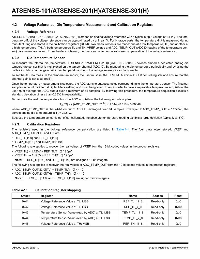
Table 4-1: Calibration Register Mapping
Offset Register Name Access Reset
0x41 Voltage Reference Value at TL: MSB REF_TL_11_8 Read-only 0x-0
0x42 Voltage Reference Value at TL: LSB REF_TL_7_0 Read-only 0x00
0x43 Temperature Sensor Value (read by ADC) at TL: MSB TEMP_TL_11_8 Read-only 0x-0
0x44 Temperature Sensor Value (read by ADC) at TL: LSB TEMP_TL_7_0 Read-only 0x00
0x45 Voltage Reference Value at TH: MSB REF_TH_11_8 Read-only 0x-0
DS60001524A-page 12 2017 Microchip Technology Inc.
ATSENSE-101/ATSENSE-201(H)/ATSENSE-301(H)
0x46 Voltage Reference Value at TH: LSB REF_TH_7_0 Read-only 0x00
0x47 Temperature Sensor Value (read by ADC) at TH: MSB TEMP_TH_11_8 Read-only 0x-0
0x48 Temperature Sensor Value (read by ADC) at TH: LSB TEMP_TH_7_0 Read-only 0x00
Table 4-1: Calibration Register Mapping
Offset Register Name Access Reset
2017 Microchip Technology Inc. DS60001524A-page 13
ATSENSE-101/ATSENSE-201(H)/ATSENSE-301(H)
4.3 Voltage Reference Value at TL: MSB
Name:REF_TL_11_8
Access:Read-only
REF_TL[11:8]: 4 MSB of REF_TL[11:0]
4.4 Voltage Reference Value at TL: LSB
Name:REF_TL_7_0
Access:Read-only
REF_TL[7:0]: 8 LSB of REF_TL[11:0]
4.5 Temperature Sensor Value at TL: MSB
Name:TEMP_TL_11_8
Access:Read-only
TEMP_TL[11:8]: 4 MSB of TEMP_TL[11:0]
4.6 Temperature Sensor Value at TL: LSB
Name:TEMP_TL_7_0
Access:Read-only
TEMP_TL[7:0]: 8 LSB of TEMP_TL[11:0]
4.7 Voltage Reference Value at TH: MSB
Name:REF_TH_11_8
Access:Read-only
REF_TH[11:8]: 4 MSB of REF_TH[11:0]
7 6 5 4 3 2 1 0
— — — — REF_TL[11:8]
7 6 5 4 3 2 1 0
REF_TL[7:0]
7 6 5 4 3 2 1 0
— — — — TEMP_TL[11:8]
7 6 5 4 3 2 1 0
TEMP_TL[7:0]
7 6 5 4 3 2 1 0
— — — — REF_TH[11:8]
DS60001524A-page 14 2017 Microchip Technology Inc.
ATSENSE-101/ATSENSE-201(H)/ATSENSE-301(H)
4.8 Voltage Reference Value at TH: LSB
Name:REF_TH_7_0
Access:Read-only
REF_TH[7:0]: 8 LSB of REF_TH[11:0]
4.9 Temperature Sensor Value at TH: MSB
Name:TEMP_TH_11_8
Access:Read-only
TEMP_TH[11:8]: 4 MSB of TEMP_TH[11:0]
4.10 Temperature Sensor Value at TH: LSB
Name:TEMP_TH_7_0
Access:Read-only
TEMP_TH[7:0]: 8 LSB of TEMP_TH[11:0]
4.11 Correction Algorithm
For H-grade products, it is possible to compensate the drift of the voltage reference by using the calibration registers described above.The following formula is used to estimate VREF at a given temperature:
where:
- VREF(ADC_TEMP_OUT): Estimated VREF value when the temperature sensor reading is ADC_TEMP_OUT- VREF(TL): VREF value at temperature TL retrieved from REF_TL[11:0]- VREF(TH): VREF value at temperature TH retrieved from REF_TH[11:0]- TEMP(TL): ADC_TEMP_OUT value at temperature TL retrieved from TEMP_TL[11:0]- TEMP(TH): ADC_TEMP_OUT value at temperature TH retrieved from TEMP_TL[11:0]
2017 Microchip Technology Inc. DS60001524A-page 15
ATSENSE-101/ATSENSE-201(H)/ATSENSE-301(H)
5. SPI Controller
5.1 Description
The SPI controller is an interface between
• the serial peripheral interface communication port• the decimation filter output data in 2’s complement format• the analog functions (ADC, LDO and reference voltage)
The SPI port provides read/write access to internal registers (Table 4-1 on page 12). This serial port features a burst transmission modewith variable data size that captures up to 7 x 32-bit ADC output results into one single access.
5.2 SPI Serial Port
5.2.1 Description
The SPI interface protocol permits writing to and/or reading registers. Moreover, a burst mode allows the fast acquisition of multipleregisters or a write on multiple registers. With this function, the size of the data can easily vary. For example, two adjacent registers canbe accessed at the same time by addressing the first register (lowest address value) and extending the quantity of serial clock edges.
The SPI interface is compatible with SPI modes 1 and 2. Data are latched on falling edges of SCLK while they are generated on the risingedges of SCLK. The idle state of SCLK can be either high or low.
5.2.2 Protocol
A transfer occurs when the NPCS signal is low. The incoming stream on MOSI is decoded on SCLK falling edge.
The first received bit indicates the direction of the operation, where 0 indicates a write and 1 a read.
The seven subsequent bits contain the address of the register to read or write.
The following bytes are data which are either emitted on the MISO line in case of a read operation, or decoded on the MOSI line in caseof a write operation.
The first data address corresponds to the first decoded address. The address pointer is then incremented each time a new byte is reador written.
The operation ends when NPCS goes high.
If NPCS goes high before the end of a byte transfer, the current byte operation is cancelled. For a read operation, no further data are senton the MISO line. For a write operation, no data is written into the currently decoded address. All previous byte operations are valid.
Figure 5-1: MODE 1 Multi-Byte Write Operation
Write A6 A0
NPCS
SCLK
MOSI
MISO
D7 D0 D7 D0
Byte to write@A[6:0]
address: A[6:0] Byte to write@A[6:0]+1
DS60001524A-page 16 2017 Microchip Technology Inc.
ATSENSE-101/ATSENSE-201(H)/ATSENSE-301(H)
Figure 5-2: MODE 2 Multi-Byte Write Operation
Figure 5-3: MODE 1 Multi-Byte Read Operation
Figure 5-4: MODE 2 Multi-Byte Read Operation
Write A6 A0
NPCS
SCLK
MOSI
MISO
D7 D0 D7 D0
Byte to write@A[6:0]
address: A[6:0] Byte to write@A[6:0]+1
Read A6 A0
NPCS
SCLK
MOSI
MISO D7 D0 D7 D0
reg(A[6:0]) reg(A[6:0]+1)address: A[6:0]
Read A6 A0
NPCS
SCLK
MOSI
MISO D7 D0 D7 D0
reg(A[6:0]) reg(A[6:0]+1)address: A[6:0]
2017 Microchip Technology Inc. DS60001524A-page 17
ATSENSE-101/ATSENSE-201(H)/ATSENSE-301(H)
6. Interrupt Controller
The Interrupt Controller generates three interrupts:
The interrupts can be detected by either polling the Interrupt Status register (ITSR) and/or by configuring the ITOUT output line. Becauseit is open-drain, this output needs to be pulled-up to VDDIO.
When activated, the ITOUT line goes low when an interrupt event occurs. It goes into Hi-Z state as soon as the interrupt source has beenreset.
Refer to “Output Interrupt Line Control Register” on page 31, “Interrupt Control Register” on page 32 and “Interrupt Status Register” onpage 32 for more information on the interrupt line configuration.
6.1 ADC Ready
The ADC_RDY interrupt rises at each new conversion frame, thus when an ADC is enabled, it reports that a new set of data is available.
It is reset either on the read of at least one ADC register (addresses from ADCI0_TAG to ADCV3_7_0) or on the read of the status register.
As the user may not need all converted values of the ADCs, only the first access to an ADC data is taken into account to reset this interrupt.
6.2 Overrun
If ADC data acquisition registers are accessed twice within the same conversion period, the OVRES interrupt rises.
It is reset on the read of the status register.
6.3 Underrun
If two synchronous signals occur without any ADC data acquisition, the UNDES interrupt rises.
It is reset on the read of the status register.
DS60001524A-page 18 2017 Microchip Technology Inc.
ATSENSE-101/ATSENSE-201(H)/ATSENSE-301(H)
7. SPI Controller User Interface
Table 7-1: Register Mapping
Offset Register Name Access Reset
0x00(2) ADCI0 TAG Register ADCI0_TAG Read-only 0x01
2017 Microchip Technology Inc. DS60001524A-page 19
ATSENSE-101/ATSENSE-201(H)/ATSENSE-301(H)
Note 1: Address value if the MSB mode is activated (see Section 7.37 ”ATSENSE Configuration Register”).
2: This register cannot be read if the MSB mode is activated (see Section 7.37 ”ATSENSE Configuration Register”).
3: Only for ATSENSE-201(H)/ATSENSE-301(H).
7.1 ADCI0 TAG Register
Name:ADCI0_TAG
Access:Read-only
TAGI0: TAG of the Anti-tamper ADC Channel
TAGI0 is equal to 1.
TEMPMEAS: Temperature Measurement Status
0: The external input of the TAMPER ADC is measured.
1: The temperature sensor input of the TAMPER ADC is measured.
DATA_VALID: I0 Channel Data Validity Status
0: The current data is not valid.
1: The current data is valid.
When the source of the ADCI0 channel switches, the decimation filter needs a few samples to stabilize its response (group delay of thefilter). Data acquired while DATA_VALID is null are not valid.
This register is not accessible if the MSB_MODE bit is enabled (see Section 7.37 on page 30).
7.2 ADCI0 Output Bits 23 to 16 Read Register
Name:ADCI0_23_16
Access:Read-only
ADCI0_23_16: Bits 23 to 16 of the Anti-tamper ADC Channel
The address value of this register depends on the value of the MSB_MODE bit (see Table 7-1 on page 19).
0x27 Analog Controls Register ANA_CTRL Read/Write 0x00
DS60001524A-page 20 2017 Microchip Technology Inc.
ATSENSE-101/ATSENSE-201(H)/ATSENSE-301(H)
7.3 ADCI0 Output Bits 15 to 8 Read Register
Name:ADCI0_15_8
Access:Read-only
ADCI0_15_8: Bits 15 to 8 of the Anti-tamper ADC Channel
The address value of this register depends on the value of the MSB_MODE bit (see Table 7-1 on page 19).
7.4 ADCI0 Output Bits 7 to 0 Read Register
Name:ADCI0_7_0
Access:Read-only
ADCI0_7_0: Bits 7 to 0 of the Anti-tamper ADC Channel
This register is not accessible if the MSB_MODE bit is enabled (see Section 7.37 on page 30).
7.5 ADCI1 TAG Register
Name:ADCI1_TAG
Access:Read-only
TAGI1: TAG of the I1 ADC Channel
TAGI1 is equal to 2.
This register is not accessible if the MSB_MODE bit is enabled (see Section 7.37 on page 30).
7.6 ADCI1 Output Bits 23 to 16 Read Register
Name:ADCI1_23_16
Access:Read-only
ADCI1_23_16: Bits 23 to 16 of the I1 ADC Channel
The address value of this register depends on the value of the MSB_MODE bit (see Table 7-1 on page 19).
7 6 5 4 3 2 1 0
ADCI0[15:8]
7 6 5 4 3 2 1 0
ADCI0[7:0]
7 6 5 4 3 2 1 0
TAGI1
7 6 5 4 3 2 1 0
ADCI1[23:16]
2017 Microchip Technology Inc. DS60001524A-page 21
ATSENSE-101/ATSENSE-201(H)/ATSENSE-301(H)
7.7 ADCI1 Output Bits 15 to 8 Read Register
Name:ADCI1_15_8
Access:Read-only
ADCI1_15_8: Bits 15 to 8 of the I1 ADC Channel
The address value of this register depends on the value of the MSB_MODE bit (see Table 7-1 on page 19).
7.8 ADCI1 Output Bits 7 to 0 Read Register
Name:ADCI1_7_0
Access:Read-only
ADCI1_7_0: bits 7 to 0 of the I1 ADC channel
This register is not accessible if the MSB_MODE bit is enabled (see Section 7.37 on page 30).
7.9 ADCV1 TAG Register
Name:ADCV1_TAG
Access:Read-only
TAGV1: TAG of the V1 ADC Channel
TAGV1 is equal to 3.
This register is not accessible if the MSB_MODE bit is enabled (see Section 7.37 on page 30).
7.10 ADCV1 Output Bits 23 to 16 Read Register
Name:ADCV1_23_16
Access:Read-only
ADCV1_23_16: Bits 23 to 16 of the V1 ADC Channel
The address value of this register depends on the value of the MSB_MODE bit (see Table 7-1 on page 19).
7 6 5 4 3 2 1 0
ADCI1[15:8]
7 6 5 4 3 2 1 0
ADCI1[7:0]
7 6 5 4 3 2 1 0
TAGV1
7 6 5 4 3 2 1 0
ADCV1[23:16]
DS60001524A-page 22 2017 Microchip Technology Inc.
ATSENSE-101/ATSENSE-201(H)/ATSENSE-301(H)
7.11 ADCV1 Output Bits 15 to 8 Read Register
Name:ADCV1_15_8
Access:Read-only
ADCV1_15_8: Bits 15 to 8 of the V1 ADC Channel
The address value of this register depends on the value of the MSB_MODE bit (see Table 7-1 on page 19).
7.12 ADCV1 Output Bits 7 to 0 Read Register
Name:ADCV1_7_0
Access:Read-only
ADCV1_7_0: Bits 7 to 0 of the V1 ADC Channel
This register is not accessible if the MSB_MODE bit is enabled (see Section 7.37 on page 30).
7.13 ADCI2 TAG Register
Name:ADCI2_TAG
Access:Read-only
TAGI2: TAG of the I2 ADC Channel
TAGI2 is equal to 4.
This register is available only in ATSENSE-201(H)/ATSENSE-301(H). In ATSENSE-201(H), it should be ignored.
This register is not accessible if the MSB_MODE bit is enabled (see Section 7.37 on page 30).
7.14 ADCI2 Output Bits 23 to 16 Read Register
Name:ADCI2_23_16
Access:Read-only
ADCI2_23_16: Bits 23 to 16 of the I2 ADC Channel
This register is available only in ATSENSE-201(H)/ATSENSE-301(H). In ATSENSE-201(H), it should be ignored.
The address value of this register depends on the value of the MSB_MODE bit (see Table 7-1 on page 19).
7 6 5 4 3 2 1 0
ADCV1[15:8]
7 6 5 4 3 2 1 0
ADCV1[7:0]
7 6 5 4 3 2 1 0
TAGI2
7 6 5 4 3 2 1 0
ADCI2[23:16]
2017 Microchip Technology Inc. DS60001524A-page 23
ATSENSE-101/ATSENSE-201(H)/ATSENSE-301(H)
7.15 ADCI2 Output Bits 15 to 8 Read Register
Name:ADCI2_15_8
Access:Read-only
ADCI2_15_8: Bits 15 to 8 of the I2 ADC Channel
This register is available only in ATSENSE-201(H)/ATSENSE-301(H). In ATSENSE-201(H), it should be ignored.
The address value of this register depends on the value of the MSB_MODE bit (see Table 7-1 on page 19).
7.16 ADCI2 Output Bits 7 to 0 Read Register
Name:ADCI2_7_0
Access:Read-only
ADCI2_7_0: Bits 7 to 0 of the I2 ADC Channel
This register is available only in ATSENSE-201(H)/ATSENSE-301(H). In ATSENSE-201(H), it should be ignored.
This register is not accessible if the MSB_MODE bit is enabled (see Section 7.37 on page 30).
7.17 ADCV2 TAG Register
Name:ADCV2_TAG
Access:Read-only
TAGV2: TAG of the V2 ADC Channel
TAGV2 is equal to 5.
This register is available only in ATSENSE-201(H)/ATSENSE-301(H).
This register is not accessible if the MSB_MODE bit is enabled (see Section 7.37 on page 30).
7.18 ADCV2 Output Bits 23 to 16 Read Register
Name:ADCV2_23_16
Access:Read-only
ADCV2_23_16: Bits 23 to 16 of the V2 ADC Channel
This register is available only in ATSENSE-201(H)/ATSENSE-301(H).
The address value of this register depends on the value of the MSB_MODE bit (see Table 7-1 on page 19).
7 6 5 4 3 2 1 0
ADCI2[15:8]
7 6 5 4 3 2 1 0
ADCI2[7:0]
7 6 5 4 3 2 1 0
TAGV2
7 6 5 4 3 2 1 0
ADCV2[23:16]
DS60001524A-page 24 2017 Microchip Technology Inc.
ATSENSE-101/ATSENSE-201(H)/ATSENSE-301(H)
7.19 ADCV2 Output Bits 15 to 8 Read Register
Name:ADCV2_15_8
Access:Read-only
ADCV2_15_8: Bits 15 to 8 of the V2 ADC Channel
This register is available only in ATSENSE-201(H)/ATSENSE-301(H).
The address value of this register depends on the value of the MSB_MODE bit (see Table 7-1 on page 19).
7.20 ADCV2 Output Bits 7 to 0 Read Register
Name:ADCV2_7_0
Access:Read-only
ADCV2_7_0: Bits 7 to 0 of the V2 ADC Channel
This register is available only in ATSENSE-201(H)/ATSENSE-301(H).
This register is not accessible if the MSB_MODE bit is enabled (see Section 7.37 on page 30).
7.21 ADCI3 TAG Register
Name:ADCI3_TAG
Access:Read-only
TAGI3: TAG of the I3 ADC Channel
TAGI3 is equal to 6.
This register is available only in ATSENSE-201(H)/ATSENSE-301(H). In ATSENSE-201(H), it should be ignored.
This register is not accessible if the MSB_MODE bit is enabled (see Section 7.37 on page 30).
7.22 ADCI3 Output Bits 23 to 16 Read Register
Name:ADCI3_23_16
Access:Read-only
ADCI3_23_16: Bits 23 to 16 of the I3 ADC Channel
This register is available only in ATSENSE-201(H)/ATSENSE-301(H). In ATSENSE-201(H), it should be ignored.
The address value of this register depends on the value of the MSB_MODE bit (see Table 7-1 on page 19).
7 6 5 4 3 2 1 0
ADCV2[15:8]
7 6 5 4 3 2 1 0
ADCV2[7:0]
7 6 5 4 3 2 1 0
TAGI3
7 6 5 4 3 2 1 0
ADCI3[23:16]
2017 Microchip Technology Inc. DS60001524A-page 25
ATSENSE-101/ATSENSE-201(H)/ATSENSE-301(H)
7.23 ADCI3 Output Bits 15 to 8 Read Register
Name:ADCI3_15_8
Access:Read-only
ADCI3_15_8: Bits 15 to 8 of the I3 ADC Channel
This register is available only in ATSENSE-201(H)/ATSENSE-301(H). In ATSENSE-201(H), it should be ignored.
The address value of this register depends on the value of the MSB_MODE bit (see Table 7-1 on page 19).
7.24 ADCI3 Output Bits 7 to 0 Read Register
Name:ADCI3_7_0
Access:Read-only
ADCI3_7_0: Bits 7 to 0 of the I3 ADC Channel
This register is available only in ATSENSE-201(H)/ATSENSE-301(H). In ATSENSE-201(H), it should be ignored.
This register is not accessible if the MSB_MODE bit is enabled (see Section 7.37 on page 30).
7.25 ADCV3 TAG Register
Name:ADCV3_TAG
Access:Read-only
TAGV3: TAG of the V3 ADC Channel
TAGV3 is equal to 7.
This register is available only in ATSENSE-201(H)/ATSENSE-301(H). In ATSENSE-201(H), it should be ignored.
This register is not accessible if the MSB_MODE bit is enabled (see Section 7.37 on page 30).
7.26 ADCV3 Output Bits 23 to 16 Read Register
Name:ADCV3_23_16
Access:Read-only
ADCV3_23_16: Bits 23 to 16 of the V3 ADC Channel
This register is available only in ATSENSE-201(H)/ATSENSE-301(H). In ATSENSE-201(H), it should be ignored.
The address value of this register depends on the value of the MSB_MODE bit (see Table 7-1 on page 19).
7 6 5 4 3 2 1 0
ADCI3[15:8]
7 6 5 4 3 2 1 0
ADCI3[7:0]
7 6 5 4 3 2 1 0
TAGV3
7 6 5 4 3 2 1 0
ADCV3[23:16]
DS60001524A-page 26 2017 Microchip Technology Inc.
ATSENSE-101/ATSENSE-201(H)/ATSENSE-301(H)
7.27 ADCV3 Output Bits 15 to 8 Read Register
Name:ADCV3_15_8
Access:Read-only
ADCV3_15_8: Bits 15 to 8 of the V3 ADC Channel
This register is available only in ATSENSE-201(H)/ATSENSE-301(H). In ATSENSE-201(H), it should be ignored.
The address value of this register depends on the value of the MSB_MODE bit (see Table 7-1 on page 19).
7.28 ADCV3 Output Bits 7 to 0 Read Register
Name:ADCV3_7_0
Access:Read-only
ADCV3_7_0: Bits 7 to 0 of the V3 ADC Channel
This register is available only in ATSENSE-201(H)/ATSENSE-301(H). In ATSENSE-201(H), it should be ignored.
This register is not accessible if the MSB_MODE bit is enabled (see Section 7.37 on page 30).
7.29 ADCI0 Controls Register
Name:SDI0
Access:Read/Write
ONADC: ADC Enable
0: ADC is disabled.
1: ADC is enabled.
When set, this bit can be read at one only after 768 µs.
TEMPMEAS: Temperature Measurement Activation
0: The external input of the TAMPER ADC is measured.
1: The temperature sensor input of the TAMPER ADC is measured.
This register must not be modified as long as the DATA_VALID bit is low (see “ADCI0 TAG Register” on page 20).
GAIN: Gain Configuration of the ADC
7 6 5 4 3 2 1 0
ADCV3[15:8]
7 6 5 4 3 2 1 0
ADCV3[7:0]
7 6 5 4 3 2 1 0
– – GAIN – – TEMPMEAS ONADC
Value Name Description
0 ADC_GAINX1 Input stage of the ADC has a gain of 1
1 ADC_GAINX2 Input stage of the ADC has a gain of 2
2 ADC_GAINX4 Input stage of the ADC has a gain of 4
3 ADC_GAINX8 Input stage of the ADC has a gain of 8
2017 Microchip Technology Inc. DS60001524A-page 27
ATSENSE-101/ATSENSE-201(H)/ATSENSE-301(H)
7.30 ADCI1 Controls Register
Name:SDI1
Access:Read/Write
ONADC: ADC Enable
0: ADC is disabled.
1: ADC is enabled.
When set, this bit can be read at one only after 768 µs.
GAIN: Gain Configuration of the ADC
7.31 ADCV1 Controls Register
Name:SDV1
Access:Read/Write
ONADC: ADC Enable
0: ADC is disabled.
1: ADC is enabled.
When set, this bit can be read at one only after 768 µs.
7.32 ADCI2 Controls Register
Name:SDI2
Access:Read/Write
This register is available only in ATSENSE-201(H)/ATSENSE-301(H). In ATSENSE-201(H), it should be ignored.
ONADC: ADC Enable
0: ADC is disabled.
1: ADC is enabled.
When set, this bit can be read at one only after 768 µs.
7 6 5 4 3 2 1 0
– – GAIN – – – ONADC
Value Name Description
0 ADC_GAINX1 Input stage of the ADC has a gain of 1
1 ADC_GAINX2 Input stage of the ADC has a gain of 2
2 ADC_GAINX4 Input stage of the ADC has a gain of 4
3 ADC_GAINX8 Input stage of the ADC has a gain of 8
7 6 5 4 3 2 1 0
– – – – – – – ONADC
7 6 5 4 3 2 1 0
– – GAIN – – – ONADC
DS60001524A-page 28 2017 Microchip Technology Inc.
ATSENSE-101/ATSENSE-201(H)/ATSENSE-301(H)
GAIN: Gain Configuration of the ADC
7.33 ADCV2 Controls Register
Name:SDV2
Access:Read/Write
This register is available only in ATSENSE-201(H)/ATSENSE-301(H).
ONADC: ADC Enable
0: ADC is disabled.
1: ADC is enabled.
When set, this bit can be read at one only after 768 µs.
7.34 ADCI3 Controls Register
Name:SDI3
Access:Read/Write
This register is available only in ATSENSE-201(H)/ATSENSE-301(H). In ATSENSE-201(H), it should be ignored.
ONADC: ADC Enable
0: ADC is disabled.
1: ADC is enabled.
When set, this bit can be read at one only after 768 µs.
GAIN: Gain Configuration of the ADC
Value Name Description
0 ADC_GAINX1 Input stage of the ADC has a gain of 1
1 ADC_GAINX2 Input stage of the ADC has a gain of 2
2 ADC_GAINX4 Input stage of the ADC has a gain of 4
3 ADC_GAINX8 Input stage of the ADC has a gain of 8
7 6 5 4 3 2 1 0
– – – – – – – ONADC
7 6 5 4 3 2 1 0
– – GAIN – – – ONADC
Value Name Description
0 ADC_GAINX1 Input stage of the ADC has a gain of 1
1 ADC_GAINX2 Input stage of the ADC has a gain of 2
2 ADC_GAINX4 Input stage of the ADC has a gain of 4
3 ADC_GAINX8 Input stage of the ADC has a gain of 8
2017 Microchip Technology Inc. DS60001524A-page 29
ATSENSE-101/ATSENSE-201(H)/ATSENSE-301(H)
7.35 ADCV3 Controls Register
Name:SDV3
Access:Read/Write
This register is available only in ATSENSE-201(H)/ATSENSE-301(H). In ATSENSE-201(H), it should be ignored.
ONADC: ADC Enable
0: ADC is disabled.
1: ADC is enabled.
When set, this bit can be read at one only after 768 µs.
7.36 Analog Controls Register
Name:ANA_CTRL
Access:Read/Write
ONBIAS: Enable of the Current Bias Generator
0: The current bias generator is disabled.
1: The current bias generator is enabled.
ONREF: Enable of the Voltage Reference
0: The voltage reference is disabled.
1: The voltage reference is enabled.
When set, this bit can be read at one after 768 µs.
ONLDO: Enable of the Internal LDO
0: The LDO is disabled.
1: The LDO is enabled.
When set, this bit can be read at one after 928 µs.
7.37 ATSENSE Configuration Register
Name:ATCFG
Access:Read/Write
OSR: OSR of the Decimation Filters
7 6 5 4 3 2 1 0
– – – – – – – ONADC
7 6 5 4 3 2 1 0
– – – – – ONLDO ONREF ONBIAS
7 6 5 4 3 2 1 0
– – – MSB_MODE – – OSR
Value Name Description
0 OSR8 OSR of the system is 8
DS60001524A-page 30 2017 Microchip Technology Inc.
ATSENSE-101/ATSENSE-201(H)/ATSENSE-301(H)
The oversampling ratio (OSR) is the ratio between the input sampling rate FSin(ADC sampling rate, typically 1.024 MHz) and the outputsampling rate FSout of the decimation filter.
The OSR must be set before switching on any ADC. Its value must not be changed if any of the ADCs are operating.
MSB_MODE: Selection Between 32-bit or 16-bit ADC Mode
7.38 ATSENSE Status Register
Name:ATSR
Access:Read-only
SYSRDY: System Ready
0: The system is not ready.
1: The system is ready.
Each time a soft or a hard reset is performed, the system operates initialization operations. ATSR indicates the end of these operations.
While ATSR is not high, no write access is possible in the registers.
7.39 Output Interrupt Line Control Register
Name:ITOUTCR
Access:Read/Write
OVRES_OUT: Overrun Output Enable
1: The OVRES interrupt activates the ITOUT output.
0: The OVRES interrupt does not activate the ITOUT output.
1 OSR16 OSR of the system is 16
2 OSR32 OSR of the system is 32
3 OSR64 OSR of the system is 64
Value Name Description
0 32BITS_MODEThe interface sends an 8-bit tag followed by the 24 bits of the ADC conversion (ADCx_TAG,ADCx_23_16, ADCx_15_8 and ADCx_7_0 registers).
1 16BITS_MODEThe interface sends the 16 MSB of the ADC conversion (ADCx_23_16 and ADCx_15_8registers). The addresses of these registers are modified while ADCx_TAG and ADCx_7_0 are nolonger readable.
7 6 5 4 3 2 1 0
– – – – – – – SYSRDY
7 6 5 4 3 2 1 0
– – – – – ADC_RDY_OUT UNDES_OUT OVRES_OUT
FSoutFSinOSR-----------=
2017 Microchip Technology Inc. DS60001524A-page 31
ATSENSE-101/ATSENSE-201(H)/ATSENSE-301(H)
UNDES_OUT: Underrun Output Enable
1: The UNDES interrupt activates the ITOUT output.
0: The UNDES interrupt does not activate the ITOUT output.
ADC_RDY_OUT: ADC Ready Output Enable
1: The ADC_RDY interrupt activates the ITOUT output.
0: The ADC_RDY interrupt does not activate the ITOUT output.
7.40 Interrupt Control Register
Name:ITCR
Access:Read/Write
OVRES_EN: Overrun Interrupt Enable
0: The generation of the overrun interrupt is disabled.
1: The generation of the overrun interrupt is enabled.
The ovres status generation should be disabled in case of access to data registers through multiple SPI accesses (not simultaneously withthe burst mode). In this case, the interrupt is generated as soon as the second access is performed.
UNDES_EN: Underrun Interrupt Enable
0: The generation of the underrun interrupt is disabled.
1: The generation of the underrun interrupt is enabled.
ADC_RDY_EN: ADC Ready Interrupt Enable
0: The generation of the ADC ready interrupt is disabled.
1: The generation of the ADC ready interrupt is enabled.
7.41 Interrupt Status Register
Name:ITSR
Access:Read-only
OVRES: Overrun Status
An overrun occurs when the host reads the data registers twice without updating the register values.
The ovres status generation should be disabled if data registers are read by multiple SPI accesses (not at once with the burst mode). Inthis case, the interrupt will be generated as soon as the second read access is performed.
This register is reset on read.
UNDES: Underrun Status
An underrun occurs when two data register updates occur without read operation.
This register is reset on read.
7 6 5 4 3 2 1 0
– – – – – ADC_RDY_EN UNDES_EN OVRES_EN
7 6 5 4 3 2 1 0
– – – – – ADC_RDY UNDES OVRES
DS60001524A-page 32 2017 Microchip Technology Inc.
ATSENSE-101/ATSENSE-201(H)/ATSENSE-301(H)
ADC_RDY: ADC Ready Status
ADC ready interrupt is generated as soon as one ADC conversion is performed.
This register is reset on read.
7.42 Software Reset Register
Name:SOFT_NRESET
Access:Write-only
NRESET: Chip Reset
When low, the entire chip is in reset state except the SPI interface and the SOFT_NRESET register.
When high, the reset state is released.
7 6 5 4 3 2 1 0
– – – – – – – NRESET
2017 Microchip Technology Inc. DS60001524A-page 33
ATSENSE-101/ATSENSE-201(H)/ATSENSE-301(H)
8. Software Example
This section details the steps to power up the ATSENSE-101/ATSENSE-201(H)/ATSENSE-301(H) devices.
1. Power the VDDIO / VDDIN plane with a 3.3V voltage.
2. If internal VDDA regulator is not used, power the VDDA pin with a 2.8V voltage.
3. If internal voltage reference is not used, power the VREF pin with a 1.2V standard voltage reference.
4. Release the internal reset:
- SPI_WRITE 0x01 @ 0x2D [SOFT_NRESET]. 5. If used, start the VDDA regulator:
- SPI_WRITE 0x04 @ 0x27 [ANA_CTRL].6. Start the analog BIAS generator:
- SPI_WRITE 0x05 @ 0x27.7. If used, start the voltage reference:
- SPI_WRITE 0x07 @ 0x27. Wait 100 ms to account for VREF settling.8. Enable the interrupts:
- SPI_WRITE 0x07 @ 0x2B [ITOUTCR],10. Start the converters:
- SPI_WRITE 0x31 @ 0x20 [SDI0], channel I0 ON with gain x8,- SPI_WRITE 0x31 @ 0x21 [SDI1], channel I1 ON with gain x8,- SPI_WRITE 0x01 @ 0x22 [SDV1], channel V1 ON,- SPI_WRITE 0x31 @ 0x23 [SDI2], channel I2 ON with gain x8,(2)
- SPI_WRITE 0x01 @ 0x24 [SDV2], channel V2 ON,(1)
- SPI_WRITE 0x31 @ 0x25 [SDI3], channel I3 ON with gain x8,(2)
- SPI_WRITE 0x01 @ 0x26 [SDV3], channel V3 ON.(2)
11. Upon interrupt line ITOUT negative edge, read the ADC conversion results in registers ranging from address 0x00 to 0x1B.
Note 1: Only for ATSENSE-201(H)/ATSENSE-301(H).
2: Only for ATSENSE-301(H).
DS60001524A-page 34 2017 Microchip Technology Inc.
ATSENSE-101/ATSENSE-201(H)/ATSENSE-301(H)
9. Electrical Characteristics (Devices with “-AU”, “-AUR”, “-SU” or “-SUR” ordering code suffix)
9.1 Absolute Maximum Ratings
Note 1: According to specifications MIL-883-Method 3015.7 (HBM - Human Body Model).
9.2 Recommended Operating Conditions
9.3 Current Consumption
Table 9-1: Absolute Maximum Ratings*
Storage temperature . . . . . . . . . . . . . . . . . . .-55°C to +150°C *NOTICE: Stresses beyond those listed under “Absolute MaximumRatings” may cause permanent damage to the device.This is a stress rating only and functional operation of thedevice at these or other conditions beyond those indi-cated in the operational sections of this specification isnot implied. Exposure to absolute maximum ratingconditions for extended periods may affect devicereliability.
Power Supply Input on VDDIO, VDDIN . . . . . . -0.3V to +4.0V
Digital I/O Input Voltage . . . . . . . . . . . . . . . . . . -0.3V to +4.0V
Analog Input Voltage on VPx, VN, IPx, INx . . . -2.0V to +4.0V
Table 9-7: Voltage Reference and Die Temperature Sensor Electrical Characteristics
Symbol Parameter Comments Min Typ Max Units
VVDDA Operating Supply Voltage – 2.7 2.8 2.9 V
IVDDA Operating Supply Current – – 70 100 µA
VREF0 Output voltage initial accuracy At TJ0 = 23°C 1.142 1.144 1.146 V
TCVREF_U
VREF drift with temperature(1)
Uncompensated – 50 –
ppm /°C TCVREF_C
Using factory programmed calibration registers.(2) – 10 –
ROUT VREF output resistance – 200 500 800 Ω
DTEMP_LinDie Temperature Sensor, Digital Reading Linearity
– – +/-2 – °C
IVREF_OFFCurrent in VREF pin when internal voltage reference is OFF
– -100 – 100 nA
Table 9-8: VDDA LDO Regulator
Symbol Parameter Comments Min Typ Max Units
VVDDIN Operating Supply Voltage – 3.0 3.3 3.6 V
IVDDIN Operating Supply Current – – – 250 µA
IO Output Current – – – 15 mA
VO DC Output Voltage IO = 0mA 2.75 2.8V 2.85 V
dVO / dIO Static Load Regulation IO: 0 to IOMAX -5 – – mV/mA
dVO/ dVVDDIN Static Line Regulation VDDIN: 3.0V to 3.6VV -5 – +5 mV/V
PSRR Power Supply Rejection Ratiof = DC to 2000 Hz – 40 –
dBf = 1 MHz – 40 –
tSTART Start-Up timeVO from 0 to 95% of final value. IO= 0mA
– – 1 ms
CO Stable Output Capacitor RangeCapacitive 0.5 1 4.7 µF
Resistive 5 10 300 mΩ
DS60001524A-page 38 2017 Microchip Technology Inc.
ATSENSE-101/ATSENSE-201(H)/ATSENSE-301(H)
10. Extended Temperature Range Electrical Characteristics (Devices with “-AN” or “-ANR” ordering code suffix)
10.1 Absolute Maximum Ratings
Note 1: According to specifications MIL-883-Method 3015.7 (HBM - Human Body Model).
10.2 Recommended Operating Conditions
10.3 Current Consumption
Table 10-1: Absolute Maximum Ratings*
Storage temperature . . . . . . . . . . . . . . . . . . .-55°C to +150°C *NOTICE: Stresses beyond those listed under “Absolute MaximumRatings” may cause permanent damage to the device.This is a stress rating only and functional operation of thedevice at these or other conditions beyond those indi-cated in the operational sections of this specification isnot implied. Exposure to absolute maximum ratingconditions for extended periods may affect devicereliability.
Power Supply Input on VDDIO, VDDIN . . . . . . -0.3V to +4.0V
Digital I/O Input Voltage . . . . . . . . . . . . . . . . . . -0.3V to +4.0V
Analog Input Voltage on VPx, VN, IPx, INx . . . -2.0V to +4.0V
DTEMP_LinDie Temperature Sensor, Digital Reading Linearity
– – +/-2 – °C
IVREF_OFFCurrent in VREF pin when internal voltage reference is OFF
– -100 – 100 nA
Table 10-8: VDDA LDO Regulator
Symbol Parameter Comments Min Typ Max Units
VVDDIN Operating Supply Voltage – 3.0 3.3 3.6 V
IVDDIN Operating Supply Current – – – 250 µA
IO Output Current – – – 15 mA
VO DC Output Voltage IO = 0mA 2.75 2.8V 2.85 V
dVO / dIO Static Load Regulation IO: 0 to IOMAX -5 – – mV/mA
dVO/ dVVDDIN Static Line Regulation VDDIN: 3.0V to 3.6VV -5 – +5 mV/V
PSRR Power Supply Rejection Ratiof = DC to 2000 Hz – 40 –
dBf = 1 MHz – 40 –
tSTART Start-Up timeVO from 0 to 95% of final value. IO= 0mA
– – 1 ms
CO Stable Output Capacitor RangeCapacitive 0.5 1 4.7 µF
Resistive 5 10 300 mΩ
DS60001524A-page 42 2017 Microchip Technology Inc.
ATSENSE-101/ATSENSE-201(H)/ATSENSE-301(H)
11. Mechanical Characteristics
Figure 11-1: 20-lead SOIC Package
2017 Microchip Technology Inc. DS60001524A-page 43
ATSENSE-101/ATSENSE-201(H)/ATSENSE-301(H)
Figure 11-2: 32-lead TQFP Package
TITLE Thin Quad Flat Pack (TQFP), 32 Pins Body: 7 x 7 x 1.0 mm Pitch 0.8 mm
GPC
AUT
DRAWING NO.
R-TQ032_E
REV .
A
Sept 20, 2012.
DS60001524A-page 44 2017 Microchip Technology Inc.
ATSENSE-101/ATSENSE-201(H)/ATSENSE-301(H)
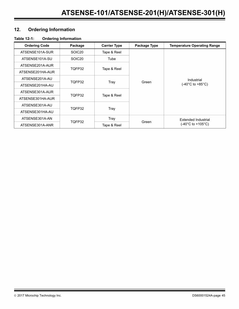
12. Ordering Information
Table 12-1: Ordering Information
Ordering Code Package Carrier Type Package Type Temperature Operating Range
ATSENSE101A-SUR SOIC20 Tape & Reel
GreenIndustrial
(-40°C to +85°C)
ATSENSE101A-SU SOIC20 Tube
ATSENSE201A-AURTQFP32 Tape & Reel
ATSENSE201HA-AUR
ATSENSE201A-AUTQFP32 Tray
ATSENSE201HA-AU
ATSENSE301A-AURTQFP32 Tape & Reel
ATSENSE301HA-AUR
ATSENSE301A-AUTQFP32 Tray
ATSENSE301HA-AU
ATSENSE301A-ANTQFP32
TrayGreen
Extended Industrial(-40°C to +105°C)ATSENSE301A-ANR Tape & Reel
2017 Microchip Technology Inc. DS60001524A-page 45
ATSENSE-101/ATSENSE-201(H)/ATSENSE-301(H)
DS60001524A-page 46 2017 Microchip Technology Inc.
13. Revision History
In the table that follows, the most recent version of the document appears first.
Table 13-1: ATSENSE-101/-201(H)/-301(H) Datasheet Rev. 60001524A Revision History
Doc. Date Changes
19-Oct-17
Updated to Microchip format. Assigned a new document number (DS60001524) and revision letter is reset to A.Document number DS60001524 revision A corresponds to what would have been 11219 revision C.ISBN number assigned.
“Atmel” changed by “Microchip” throughout.
Added 105°C devices in the “Ordering Information” section and the corresponding “Extended TemperatureRange Electrical Characteristics (Devices with “-AN” or “-ANR” ordering code suffix)” section.
Clarified maximum current spec in “Absolute Maximum Ratings” section.
Removed IVDDx OFF current specification in Table 10-6, Table 10-7 and Table 10-8 as they cannot bemeasured individually.
Table 13-2: ATSENSE-101/-201(H)/-301(H) Datasheet Rev. 11219B Revision History
Doc. Date Changes
20-Feb-14
Removed preliminary status.
ATSENSE-201(H) device added to the datasheet in “Description” and “Features”.
Section 2. “Package and Pinout”: added ATSENSE-201(H)
Updated register descriptions for use with ATSENSE-201(H) from “ADCI2 TAG Register” to “ADCV3 Output Bits 7 to 0 Read Register” and from “ADCI2 Controls Register” to “ADCV3 Controls Register”.
Section 9.6 “Measurement Channels”, Section 9.7 “Voltage Reference and Die Temperature Sensor” and Section 9.8 “VDDA LDO Regulator”: In introduction text, corrected CVREFand CVDDA units to µF.
Table 9-6 “Measurement Channel Electrical Characteristics”: Added condition with typ value for SINADPEAK
Table 9-8 “VDDA LDO Regulator”: Updated min, typ and max values and modified units for parameters Static Load Regulation and Static Line Regulation. Changed typ value for parameter Power Supply Rejection Ration for condition f = 1 MHz.
Table 13-3: ATSENSE-101/-301(H) Datasheet Rev. 11219A 15-Oct-13 Revision History
Doc. Date Changes
15-Oct-13 First Issue
2017 Microchip Technology Inc. DS60001524A-page 47
ATSENSE-101/ATSENSE-201(H)/ATSENSE-301(H)
The Microchip Web Site
Microchip provides online support via our web site at www.microchip.com. This web site is used as a means to makefiles and information easily available to customers. Accessible by using your favorite Internet browser, the web sitecontains the following information:
• Product Support – Data sheets and errata, application notes and sample programs, design resources, user’sguides and hardware support documents, latest software releases and archived software
• General Technical Support – Frequently Asked Questions (FAQ), technical support requests, online discussiongroups, Microchip consultant program member listing
• Business of Microchip – Product selector and ordering guides, latest Microchip press releases, listing of seminars and events, listings of Microchip sales offices, distributors and factory representatives
Customer Change Notification Service
Microchip’s customer notification service helps keep customers current on Microchip products. Subscribers will receivee-mail notification whenever there are changes, updates, revisions or errata related to a specified product family ordevelopment tool of interest.
To register, access the Microchip web site at www.microchip.com. Under “Design Support”, click on “Customer ChangeNotification” and follow the registration instructions.
Customer Support
Users of Microchip products can receive assistance through several channels:
• Distributor or Representative
• Local Sales Office
• Field Application Engineer (FAE)
• Technical Support
Customers should contact their distributor, representative or Field Application Engineer (FAE) for support. Local salesoffices are also available to help customers. A listing of sales offices and locations is included in the back of thisdocument.
Technical support is available through the web site at: http://microchip.com/support
DS60001524A-page 48 2017 Microchip Technology Inc.
Product Identification System
To order or obtain information, e.g., on pricing or delivery, refer to the factory or the listed sales office.
Product Series
Product Number
ATSENSE301HA - AUR
Temperature Range
Mask Revision
Package
Carrier Type
Accuracy Grade
Product Series: ATSENSE = ATSENSE series
Product Number: 101 = Single-Phase (1 Voltage + 2 Current Channels) 201 = Dual-Phase (2 Voltage + 2 Current Channels)301 = Poly-Phase (3 Voltage + 4 Current Channels)
Accuracy Grade: Blank = Standard AccuracyH = High Accuracy
Mask Revision: A = Revision A
Package: A = TQFP32S = SOIC20
Temperature Range:
U = -40°C to +85°C (Industrial)N = -40°C to +105°C (Extended Industrial)
Carrier Type: Blank = Standard Packaging (tube or tray)R = Tape and Reel (1)
Example:
a) ATSENSE301HA-AUR = 3-Phase (3xV + 4xI)
ATSENSE, High accuracy grade, Industrial
Temperature Range, TQFP32 Package, Tape
and Reel Carrier
Note 1: Tape and Reel identifier only appears in thecatalog part number description. This identi-fier is used for ordering purposes and is notprinted on the device package. Check withyour Microchip Sales Office for packageavailability with the Tape and Reel option.
2: Small form-factor packaging options may beavailable. Please check www.micro-chip.com/packaging for small-form factorpackage availability, or contact your localSales Office.
Note the following details of the code protection feature on Microchip devices:
• Microchip products meet the specification contained in their particular Microchip Data Sheet.
• Microchip believes that its family of products is one of the most secure families of its kind on the market today, when used in theintended manner and under normal conditions.
• There are dishonest and possibly illegal methods used to breach the code protection feature. All of these methods, to ourknowledge, require using the Microchip products in a manner outside the operating specifications contained in Microchip’s DataSheets. Most likely, the person doing so is engaged in theft of intellectual property.
• Microchip is willing to work with the customer who is concerned about the integrity of their code.
• Neither Microchip nor any other semiconductor manufacturer can guarantee the security of their code. Code protection does notmean that we are guaranteeing the product as “unbreakable.”
Code protection is constantly evolving. We at Microchip are committed to continuously improving the code protection features of ourproducts. Attempts to break Microchip’s code protection feature may be a violation of the Digital Millennium Copyright Act. If such actsallow unauthorized access to your software or other copyrighted work, you may have a right to sue for relief under that Act.
Legal Notice
Information contained in this publication regarding device applications and the like is provided only for your convenience and may besuperseded by updates. It is your responsibility to ensure that your application meets with your specifications. MICROCHIP MAKES NOREPRESENTATIONS OR WARRANTIES OF ANY KIND WHETHER EXPRESS OR IMPLIED, WRITTEN OR ORAL, STATUTORY OROTHERWISE, RELATED TO THE INFORMATION, INCLUDING BUT NOT LIMITED TO ITS CONDITION, QUALITY, PERFORMANCE,MERCHANTABILITY OR FITNESS FOR PURPOSE. Microchip disclaims all liability arising from this information and its use. Use ofMicrochip devices in life support and/or safety applications is entirely at the buyer’s risk, and the buyer agrees to defend, indemnify andhold harmless Microchip from any and all damages, claims, suits, or expenses resulting from such use. No licenses are conveyed, implic-itly or otherwise, under any Microchip intellectual property rights unless otherwise stated.
Trademarks
The Microchip name and logo, the Microchip logo, AnyRate, AVR, AVR logo, AVR Freaks, BeaconThings, BitCloud, CryptoMemory,CryptoRF, dsPIC, FlashFlex, flexPWR, Heldo, JukeBlox, KeeLoq, KeeLoq logo, Kleer, LANCheck, LINK MD, MediaLB, MOST, MOSTlogo, MPLAB, OptoLyzer, PIC, picoPower, PICSTART, PIC32 logo, Prochip Designer, QTouch, RightTouch, SAM-BA, SpyNIC, SST,SST Logo, SuperFlash, tinyAVR, UNI/O, and XMEGA are registered trademarks of Microchip Technology Incorporated in the U.S.A.and other countries.
ClockWorks, The Embedded Control Solutions Company, EtherSynch, Hyper Speed Control, HyperLight Load, IntelliMOS, mTouch,Precision Edge, and Quiet-Wire are registered trademarks of Microchip Technology Incorporated in the U.S.A.
Adjacent Key Suppression, AKS, Analog-for-the-Digital Age, Any Capacitor, AnyIn, AnyOut, BodyCom, chipKIT, chipKIT logo,CodeGuard, CryptoAuthentication, CryptoCompanion, CryptoController, dsPICDEM, dsPICDEM.net, Dynamic Average Matching,DAM, ECAN, EtherGREEN, In-Circuit Serial Programming, ICSP, Inter-Chip Connectivity, JitterBlocker, KleerNet, KleerNet logo, Mindi,MiWi, motorBench, MPASM, MPF, MPLAB Certified logo, MPLIB, MPLINK, MultiTRAK, NetDetach, Omniscient Code Generation,PICDEM, PICDEM.net, PICkit, PICtail, PureSilicon, QMatrix, RightTouch logo, REAL ICE, Ripple Blocker, SAM-ICE, Serial Quad I/O,SMART-I.S., SQI, SuperSwitcher, SuperSwitcher II, Total Endurance, TSHARC, USBCheck, VariSense, ViewSpan, WiperLock,Wireless DNA, and ZENA are trademarks of Microchip Technology Incorporated in the U.S.A. and other countries.
SQTP is a service mark of Microchip Technology Incorporated in the U.S.A.
Silicon Storage Technology is a registered trademark of Microchip Technology Inc. in other countries.
GestIC is a registered trademarks of Microchip Technology Germany II GmbH & Co. KG, a subsidiary of Microchip Technology Inc., inother countries.
All other trademarks mentioned herein are property of their respective companies.
2017 Microchip Technology Inc. DS60001524A-page 49
Quality Management System Certified by DNV
ISO/TS 16949
Microchip received ISO/TS-16949:2009 certification for its worldwide headquarters, design and wafer fabrication facilities in Chandlerand Tempe, Arizona; Gresham, Oregon and design centers in California and India. The Company’s quality system processes and pro-cedures are for its PIC® MCUs and dsPIC® DSCs, KEELOQ® code hopping devices, Serial EEPROMs, microperipherals, nonvolatilememory and analog products. In addition, Microchip’s quality system for the design and manufacture of development systems is ISO9001:2000 certified.
DS60001524A-page 50 2017 Microchip Technology Inc.
DS60001524A-page 51 2017 Microchip Technology Inc.
AMERICASCorporate Office2355 West Chandler Blvd.Chandler, AZ 85224-6199Tel: 480-792-7200 Fax: 480-792-7277Technical Support: http://www.microchip.com/supportWeb Address: www.microchip.com
AtlantaDuluth, GA Tel: 678-957-9614 Fax: 678-957-1455
Austin, TXTel: 512-257-3370
BostonWestborough, MA Tel: 774-760-0087 Fax: 774-760-0088
ChicagoItasca, IL Tel: 630-285-0071 Fax: 630-285-0075