Page 1
MULTIFUNCTIONAL MATERIAL DIRECT PRINTING FOR LASER SINTERING
SYSTEMS
C. E. Folgar
1, L. N. Folgar
1, and D. Cormier
2
13D Systems Corporation, Rock Hill, SC 29730
2Industrial and Systems Engineering Department,
Rochester Institute of Technology, Rochester, NY 14623
Abstract
The research reports the development of advanced techniques for the direct print of
materials into parts made by laser sintering. The present invention provides for the production of
three-dimensional objects with improved build and support materials. The direct printed material
may be metals, elastomers, ceramic, or any other material, which is typically different than the
laser sintering material. Aspects of the technique include direct printed materials within laser
sintered parts to improve part strength, provide multi-materials, provide electrical conductivity,
and provide other desirable benefits to the part.
Introduction
The ability to fabricate smart structures using multifunctional materials is an area of
interest for the manufacturers of autonomous systems. Additive manufacturing (AM) provides
the flexibility of fabricating complex shapes and monolithic structures that can reduce part count
and increase mission readiness by reducing the lead times to fabricate these structures. An AM
process that offers the robustness of functional parts and the flexibility of utilizing
multifunctional materials would disrupt the way in which such systems are designed and the way
in which they operate increasing and expanding the spectrum of mission capabilities (e.g.
intelligence, reconnaissance, surveillance, sensing).
The need to achieve light weight multifunctional materials led to the development of
carbon fiber composites and carbon nanocomposites. There is an on-going demand and need
from costumers’ applications to fabricate multifunctional parts with embedded electronics (e.g.
antennas, sensors, wiring and circuitry). In the solar panel manufacture industry Direct-Write
(DW) technologies are widely used to trace Silver (Ag) lines down to 10µm to collect solar
energy. In a similar manner this technique has been used by several companies to trace
conformal antennas, strain sensors, and conductive lines in helmets and aircraft wings. Systems
such as Aerosol Jet (AJ), SmartPump, and MicroPen deposition among several others, are being
used to print conductive material, and embedded circuitry onto the surface of parts.
Embedding electrical components to the body of structures has acquired the attention of
the AM industry [1], where manufacturing costs and turn-around lead times are critical for the
production scenario. Direct-Write of the electrical components not only allows for cost reduction
and better turn-around time; it allows for payload reduction and concealed electrical components.
With the technological advances in material development for the rapid prototyping
applications, the aerospace industry has adopted Selective Laser Sintering as the preferred
manufacturing method for non-structural aerospace components. The advantage of the SLS
282
Page 2
process is the turn-around lead time that is involved with manufacturing a part. Once a CAD
model has been created, it is sent to an SLS machine for manufacturing.
The versatility provided by the SLS process to manufacture parts; and the practicality of
Direct-Write to produce embedded electronics, make the combination of the technologies a novel
method to incorporate multifunctional materials into autonomous systems structures. Some of the
key advantages that embedded electronics offer to the manufacture of aerospace structures, and
the Direct Part Manufacture industry in general, are:
Payload reduction through electrical wiring reduction
Concealed electrical components within the part
Parts turn-around cost
Start-to-finish part productions lead times.
Multifunctional Material Incorporation Into Additive Manufactured Structures
The most suitable AM technologies to integrate an in-situ hybrid direct write (DW) rapid
manufacturing method use amorphous and semi crystalline polymers as extruded filaments or
deposited powders. The most successful bonding mechanism for this application is typically
laser consolidation/fusion. These AM processes of choice include Stereolithography (SLA),
Fused Deposition Modeling (FDM), Selective Laser Sintering (SLS), and Selective Heat
Sintering (SHS). The combination of technologies has focused on tracing conductive material on
the surface of parts with DW methods; thus achieving multi-functionality within the material.
The Direct-Write term covers a wide range of printing methods that follows the same principle
of fabrication: deposition of material on two or three-dimensional structures through a stationary
nozzle, with a motion-controlled substrate that determines the location of material deposition.
Paramount was able to demonstrate the proof of feasibility study of combining two
additive manufacturing (AM) techniques to fabricate a part with embedded traces of conductive
ink using thermoplastic materials. Compatibility of Nylon12 substrates to conductive inks was
evaluated in collaboration with the Rochester Institute of Technology. Cabot CSD-32 was used
with Optomec’s Aerosol Jet, and 40-3920R HVA was used with nScrypt’s SmartPump system.
The adhesion and flexibility of the inks was demonstrated with a 3-point-bend test designed to
print traces of conductive ink on SLS tensile bars.
The viability of performing in-situ printing traces of conductive Ag (4020R HVA
dissolved in 15 - 25 wt% Xylene) was also proven at Paramount by retrofitting an open source
3D printer (Fab@Home) to a 2500-CI SLS platform. An ASTM D-638 test bar was produced
with the laser scanner; a conductive trace was printed on top of the sintered Nylon surface, and a
layer of powder was rolled over and sintered to finish the test bar. Conductivity was tested with a
Fluke 28II TRMS multi-meter where a resistance of 0.3 Ω was shown along the XY-axis of the
SLS process.
283
Page 3
Embedded Sensors Fabrication Feasibility Using Additive Technologies
Feasibility of combining SLS with a direct-write technology was assessed in 3 phases.
Each phase would study the feasibility of retrofitting a base technology in order to create a
hybrid process.
Phase 1.1: Presented and compared available AM technologies that are compatible
with the physics of the SLS process.
Phase 1.2: Studied the feasibility of incorporating the SLS process within a DW
technology.
Phase 1.3: Evaluated DW technologies inside the SLS process.
Phase 1.1 studied existing technologies that were considered practical for the deposition
of conductive inks and compatible with the physics of the SLS process. There are several DW
technologies in the market that are used to print electronics. The complexity and packaging of
some of these prevents them from being easily adapted with an additional internal module to
perform SLS of polymers inside them. Several technologies were evaluated and their
characteristics are summarized in Table 1.
System Deposition Viscosity Interaction Temperature Setup AEROSOL JET
Optomec Hydrodynamic 1 – 1E3cP Contact-less 24 - 150°C OEM
MICROPEN
MicroPen Technologies Micro-capillary 5 – 5E5 cP Surface Contact 24 °C Custom
SMARTPUMP
nScrypt Micro-dispense 1 – 1E6 cP Surface Contact 24 - 150°C OEM
FAB@HOME
Seraph Robotics Extrusion 1 – 3E9 cP Substrate Contact 24°C OEM
Table 1. Summary of Systems Considered for Proof-of-Concept Study
Aerosol Jet®, by Optomec, is a mask-less, meso-scale, material deposition system that
uses hydrodynamic deposition of atomized aerosol particles, and a motion-controlled system
which allows for creation of complex patterns on the substrate without making contact with the
surface. The Aerosol Jet process starts with the atomization of a liquid sample of the material to
print, creating a dense aerosol of droplets with diameters between 1 and 5 microns that are
transported to the deposition head using an inert carrier gas (Figure 1: A-C).
MicroPen® writing system, by MicroPen Technologies, is a micro-capillary technology
where a pen tip “rides” on the surface of the material without touching the substrate surface
(Figure 1: D-E). It uses a proprietary positive displacement pumping method to control ink
volume of flowable materials onto a surface.
SmartPump™
, by nScrypt, uses a micro-dispense pump to deposit material onto the
substrate of contact. It uses positive pressure and a computer controlled needle valve that
provides active valving and suck-back to control flow characteristics (Figure 1: F-H).
284
Page 4
Aer
oso
l Jet
®
(A) AJ process: Ink droplets form
in the atomizer and travel to the
nozzle for deposition
(B) Contactless nozzle head of the
AJ system
(C) Optomec Aerosol Jet System
Mic
roP
en®
(D) The plunger of a syringe
loaded with material forces the
ink into the micro-capillary
writing tip
(E) Close-up of the micro-
capillary writing tip
nS
cryp
t
(F) nScrypt Deposition Close-up
(G) A computer controlled needle
valve provides active valving to
control flow characteristics at
start – stop
(H) nScrypt SmartPump System
Figure 1: Direct Write systems evaluated in the feasibility study for application with Selective Laser
Sintering: Aerosol Jet, MicroPen, and SmartPump.
Study Conductive Wire/3d Printing For Integrated Antennas/Sensors
Phase 1.2 studied the option of having the SLS process adapted within a DW technology.
The DW technologies selected were Aerosol Jet and SmartPump systems, both available at RIT.
Each technology uses a special Silver base ink and the resolution improves by using the
manufacturer’s recommended ink. Cabot CSD-32 was used for the Optomec system and 40-
3920R HVA for the nScrypt equipment; the viscosity of both inks was adjusted for printing the
conductive material on Nylon 12 (PA12) substrate.
A B C
D E
F G H
285
Page 5
DW/SLS Experimental Setup
Aerosol Jet technology from Optomec was used as a base board to adapt an engineered
fixture that would mimic the SLS environment. The flexibility of the system allowed enough
room to implement a miniature powder bed where Nylon12-substrate conditions could be tested.
Paramount designed a material delivery mechanism that mimics the deposition method in the
laser sintering process. The goal was to document the technical challenges involved in the
fabrication of parts with embedded sensors via a combination of selective laser sintering coupled
with direct-write technologies. The main technical objective is to demonstrate the feasibility of
embedding conductive paths in-situ during the laser sintering of polymers.
The miniature SLS fixture shown in Figures 2-3 consisted of a powder reservoir partition
were powder was placed and then spread across a moving z-axis stage with 10 mm travel
distance. The leveling of powder was done with a straight edge. The part bed lowering/rising
mechanism used a micrometer screw to level the powder bed in 0.004-0.005” layer thickness
increments.
Thin silicone heating pads were placed at the bottom and side walls of the SLS fixture to
achieve melting of the PA12 powder at 175°C. A radiant heating strip was placed above the
powder bed to maintain a variable current open-loop heating source to control the processing
temperature of the polymer surface. An external 40W CO2 laser was used to melt the nylon.
Layers of PA12 where sintered with the laser system and then quickly transferred the powder
bed spreader fixture to the AJ system.
Figure 2: Powder Delivery Mechanism for the Feasibility Study of SLS/Direct-Write Hybrid AM Process
Part
Piston
Overflow
Bin
Feed
Piston
Micrometer
Z-height Control
Bottom
Plate
286
Page 6
Figure 2 shows Paramount’s designs and the fabricated parts for the material delivery
mechanism. The system uses a micrometer to control the vertical travel of the part piston
controlling the z-height (layer thickness) in 0.004-0.005” increments.
The mechanism was installed and tested as shown in Figure 3. This mechanism is
heated from the bottom utilizing the heat from the platen of the Optomec Aerosol Jet Machine.
A method to heat the top of the powder bed during sintering is necessary and proved to be very
difficult to implement. The heat from the machine’s bottom plate is keeping the sintered powder
from curling up but this will become a challenge as more layers are consolidated in the z-
direction.
Figure 3: Powder Delivery Mechanism Installed in the Aerosol Jet Machine at Rochester Institute of
Technology for the Feasibility Study of SLS/Direct-Write Hybrid AM Process
Paramount provided several laser sintered Nylon-12 samples to RIT for the purpose of
testing ink adhesion to the Nylon 12 substrate. These samples were carefully fabricated to show
two different surface finishes that may be present during the laser sintering process. The first
case is when a fresh layer of polymer powder is deposited on top of a previously sintered layer
resulting in a rough surface formed by the partially bonded particles on top of the sintered
polymer matrix. The second case shows the surface roughness present during an interim stage
(fully molten layer) in between scans. In this later case the sintered layer was removed from the
fabrication area immediately after the laser stopped scanning prior to the next recoat. The goal
is to examine the microstructure of the conductive traces on both types of surfaces. This
microstructure needs to be uniform to maintain good conductivity at the interlayer (in the Z-
plane) after the new layer of powder is deposited (Figure 5).
Aerosol Jet and nScrypt technologies were used to print silver inks on the surfaces of
these samples (Figure 4). The preliminary specimens are showing high electrical conductivity
when measured with a regular ohm meter. Paramount will require more funding to perform
more extensive studies to measure and baseline the volume and surface resistivity with the
proper equipment. Table 2 summarizes the DOE for printing conductive inks in multiple
material substrates. Table 3 shows a comparison of the multiple inks utilize for these
experiments.
287
Page 7
System Substrate Ink Result Aerosol Jet Fluff Powder CSD-32 Fail
Sintered Powder CSD-32 Success
Part Surface CSD-32 Success
SmartPump Fluff Powder 40-3920R HVA Fail
Sintered Powder 40-3920R HVA N/A
Part Surface 40-3920R HVA Success Table 2. Design of Experiment Followed to Test System and Ink Compatibility to PA12
Figure 4: Traces of Silver Ink Printed on Laser Sintered Nylon-12 using A) Aerosol Jet® and B) nScrypt
Direct-Write Technologies
CSD-32 40-3920R HVA
Deposition System Aerosol Jet® SmartPump™
Conductive Metal Silver Silver
Ink Form Liquid Paste
Metal Content 45 – 55 wt% 85 wt%
Viscosity 11 – 15 Cps @ 25°C 9,000 Cps @ 25°C
Cure Temperature 100°C – 300°C 100°C – 150°C
Volume Resistivity 0.004 – 0.080 Ω∙cm 0.001Ω∙cm
Compatible to Ceramics, Metals, Plastics, Circuit
Boards
Ceramics, Metals, Plastics, Circuit
Boards
Applications
Membrane Switches, Flexible
Circuits, Polymer Thick Film
Circuits, and EMI/RFI shielding
Membrane Switches, Flexible
Circuits, Polymer Thick Film
Circuits, and EMI/RFI shielding
Table 3. Comparison of Conductive Inks used in the Proof-of-Concept Experiments
A B
288
Page 8
Figure 5: Conductive Ink Printed on PA12 Samples and then “Sandwiched” with a Second Layer of PA12 (A)
Cabot CSD-32 Ag Ink Printed with AJ (B) 40-3920R HVA Ag Ink Printed with SmartPump™
Experimental Results
Nylon Tensile bars were produced on a 3DS S-Pro60 SLS machine to evaluate ink wear
behavior under stress. A conductive print trace on a tensile bar measuring 10.16cm long and
0.3175cm wide and 10 layers thick (approximately 0.00562cm) was tested at different distances
with a multi-meter to demonstrate connectivity along the trace. Results were compared to
theoretical data calculated with equation
(1)
Where ρ is the resistivity of the material measured in [Ω∙cm], L is the length of the
conductive trace, and A is the cross-sectional area. Although the resistivity is higher than
expected, the results are promising at the stage of the study. Electrical conductivity was not lost
during strain test applied to the part is shown in Figure 6 below.
C
A B
A B
289
Page 9
Figure 6: (A-B) Bending Test Setup used to Determine Conductive-Trace Wear and Durability under
Flexural Load. Resistance Increases as Deflection Increases. (C-D) Resistance Readings vs. Deflection
Distance and Distance between Proves
The resistance values from Figure 6 show how the electrical conductivity is recovered or
goes nearly back to its original value after the load was removed. This particular experiment
proved the feasibility of being able to print a strain gauge on the surface of an SLS part.
CSD-32 ink printed with AJ shows good deposition, flexibility and adhesion to the PA
substrates. Aerosol Jet demonstrates to be a cleaner deposition method than nScrypt’s
SmartPump. Optomec’s contactless deposition makes it a more suitable candidate for conformal
deposition of conductive material to a produced part. Some of the advantages and disadvantages
of Aerosol Jet system are:
Contact-less deposition allows for clean prints.
Ability to modify trace width and thickness without switching deposition head.
Ink curing temperatures range between SLS processing temperatures.
Droplet carrier/focusing sheath gas creates a cloud of powder in surrounding print area.
Sheath gas creates a localized crystallization/solidification phase at the trace pattern.
Localized layer bonding quality decrease due to localized solidification.
The 40-3920R HVA ink used with nScrypt’s SmartPum was more difficult to apply and
to manage its print resolution. In contrast to Aerosol Jet, the SmartPump prints thicker traces of
material against the surface of contact. Some of the advantages and disadvantages of the
SmartPum systems are:
System deposits material without disturbing the surrounding print area.
Ink curing temperatures range within SLS processing temperatures.
Deposition requires indirect (substrate/ink/tip) contact with the substrate.
Trace width and thickness are modified by changing the deposition head.
Demonstrate Fabrication Feasibility Using SLS and 3DP
Phase 3 evaluated the behavior of the Direct Write method within the SLS environment
using a laser sintering machine. This effort required the design and modification of an apparatus
that was adapted to the SLS machine to make possible the in-situ deposition of conductive ink
within the SLS process. The feasibility of printing traces of conductive Silver ink (4020R HVA
dissolved in 15 - 25 wt% Xylene) was proven by retrofitting an open source 3D printer
(Fab@Home) to a 2500-CI SLS platform. ASTM D-638 test bars were produced with the SLS
laser and conductive traces were printed in-situ on the molten nylon substrate. The layer wise
process was repeated by adding a layer of powder over and sintering until the test bar was
D
290
Page 10
completed. The conductivity of the embedded conductive traces was tested with a Fluke 28-II
TRMS multi-meter and a resistance of 0.3 Ω was reported along the XY-axis of the SLS process
(Figure 90).
Experimental Setup
The Aerosol Jet and SmartPump systems previously studied were not considered as an
option for this experimental phase due to the required cost, time, and the support from OEMs to
develop custom-made components and software modifications. The integration of a DW to an
existing SLS system was performed by retrofitting a Fab@Home 3D printer to fit the frame of a
DTM 2500CI SLS system (Figure 7).
Figure 7: Fab@Home Uses Open Source Software to Create Files that are Sent to the Equipment for Printing
The Fab@Home printer is fabricated with acrylic sheets that are laser-cut in a “puzzle”
like configuration. It uses 2D parts to build a 3D structural part. Some of the modifications that
needed to take into account to be able to use the machine in the SLS equipment are:
Reduce frame size from 16.15in high to 6.29in to fit in the SLS machine.
Use a heat resistant material to withstand 175°C without deformation.
Design a rail mechanism to insert and remove the printer fixture.
The Fab@Home printer was redesigned to meet the requirements that would allow the
fixture to slide in and out of the SLS machine without difficulty (Figure 8 - 9). The Fixture was
modified in SolidWorks and re-designed to be built in as fewer parts.
Figure 8: CAD Modeling of the Retrofitted Prototype 3D Printer
291
Page 11
The prototype was fabricated in a EOS P-730 machine, with a 38% glass-filled PA 12
build the entire fixture in one part. The retrofitted printer frame was made with Aluminum to
address the PA12 processing temperature at 175°C, required to melt the powder. For
experimental purposes the printer fixture needed to withstand the SLS environment for at least 2
minutes without deforming structural parts.
Figure 9: Aluminum 3D Printer Inside the SLS Machine During Testing
Experimental Results
Traces of conductive ink (4020R HVA dissolved in 15 - 25 wt% Xylene) were printed
inside a 2500-CI SLS platform. ASTM D-638 test bars were produced with the laser scanner; a
conductive trace was printed on top of the sintered Nylon surface, and a layer of powder was
rolled over and sintered to finish the test bar. The deposition methods were varied in order to
determine the optimum deposition sequence to produce parts with embedded conductive traces.
The experimental sequences are illustrated in Figure 10 and 11 below.
Figure 10. Sintering and Printing Configurations used to Produce SLS Parts with Embedded Conductive
Paths. Configurations that Required Deposition of Ink before Laser Sintering Failed to Produce a
Complete Part
292
Page 12
The goal of the preliminary tests was to prove functionality, flow-ability and conductivity
of the ink on the XY plane as show in Figure 12. The steps followed to produce hybrid parts
were:
1. Inert process chamber and warm-up Nylon 12 powder
2. 30 min. SLS build warm-up stage
3. Test bars begin to sinter layers
Process pause
3D printer slide in and setup (Figure 11 A)
Conductive ink deposition (Figure 11 B)
3D printer slide out (Figure 11 C)
Process resume
4. Roller puts down powder
5. Sintering of a layer
Process pause
3D printer slide in and setup
Conductive ink deposition
3D printer slide out
Process resume
6. Sintering continues to finish
Figure 11. In-situ DW/SLS Stages during Printing and Deposition
Figure 12: Fabricated Parts with Embedded Ag-ink Traces Embedded in PA12 SLS Bars Demonstrate a
Novel Technique for Embedded Sensor Printing
A B C
Material Deposition Roller Direction Material Deposition Roller Direction
293
Page 13
Electrical conductivity in the Z direction will be a challenge for any AM process with
polymers. The layers deposited act as insulating barriers that prevent the electrical conductivity
through them in the Z direction. Any hybrid process must consider a way to mitigate this
technical challenge. This study, however, demonstrated signs of feasibility by showing
conductivity through multiple traces of Silver ink printed between alternating layers (different z-
heights). The DOE was limited to DW through only 5 layers sandwiched in the mid-section of a
standard tensile bar fabricated via SLS. The results presented in Figure 13 show electrical
conductivity readings ranging between 0.3Ω (1-2), to 6.4Ω (4-5).
Figure 13: Electrical Conductivity Demonstrated in the Z-Direction for Multilayer Experiments, for a 5-
Layer DW/SLS Printed Section of an SLS Tensile Bar
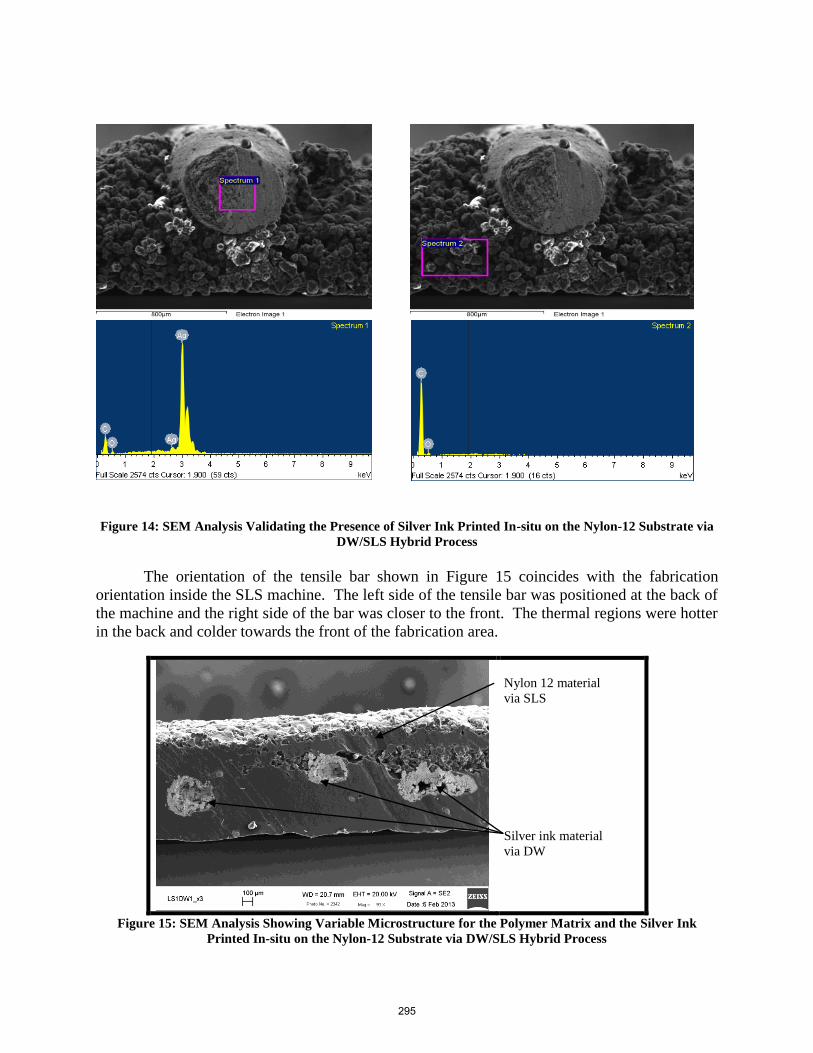
An SEM analysis was conducted to study and document the microstructure of the silver
deposited on the nylon 12 as a polymer substrate. The results are presented in Figures 14-15
showing a single trace of Ag printed in-situ on top of a previously melted [by the CO2 laser]
layer of nylon 12. The polymer matrix shown in Figure 14 appears to be very porous showing
regions only partially melted.
This microstructure is an artifact of unstable an inconsistent processing temperatures
inside the SLS processing chamber during this experiment. The processing-temperature set
points fluctuated as much as 20-30◦C due to the alterations made to the latching and seal
mechanisms of the front door of the SLS machine. These engineering modifications were
required to allow for the insertion and extraction of the fixture holding the DW extruding print
head. Figure 15 shows the microstructure of the cross section of an SLS tensile bar with
embedded traces of silver ink printed in-situ at different z-heights. The microstructure of Figure
15 also shows a variation in density from left to right going from fully dense to porous. The
variable density is shown not only within the polymer matrix, but also in the deposited silver ink
with the adverse density effect worsening in the same direction (left to right). This phenomenon
was caused by the same thermal gradients (hot and cold regions) introduced by the opening and
closing of the door.
294
Page 14
Figure 14: SEM Analysis Validating the Presence of Silver Ink Printed In-situ on the Nylon-12 Substrate via
DW/SLS Hybrid Process
The orientation of the tensile bar shown in Figure 15 coincides with the fabrication
orientation inside the SLS machine. The left side of the tensile bar was positioned at the back of
the machine and the right side of the bar was closer to the front. The thermal regions were hotter
in the back and colder towards the front of the fabrication area.
Nylon 12 material
via SLS
Silver ink material
via DW
Figure 15: SEM Analysis Showing Variable Microstructure for the Polymer Matrix and the Silver Ink
Printed In-situ on the Nylon-12 Substrate via DW/SLS Hybrid Process
295
Page 15
Conclusion
3D Systems has proven the ability to use multiple additive manufacturing technologies
for the fabrication of complex parts with embedded sensors using direct-write/direct-print
technologies combined with the laser sintering (LS) process and laser sintering materials. The
versatility provided by the SLS process to manufacture parts; and the practicality of Direct-Write
to produce embedded electronics, make the combination of the technologies a novel method to
incorporate multifunctional materials into autonomous systems structures. This novel additive
manufacturing technique provides for the ability to improve part strength, provide multi-
materials, provide electrical conductivity, and provide other desirable benefits to the part.
Acknowledgements
The research presented here was funded through contract number FA8650-10-C-5705 by
the United States Air Force Research Laboratory with funding provided by the Defense-wide
Manufacturing Science and Technology Program through the Office of the Secretary of Defense,
Manufacturing and Industrial Base Policy.
SLS is a registered trademark of 3D Systems Corp. Aerosol Jet is a registered trademark of Optomec. MicroPen is a
registered trademark of MicroPen Technologies. SmartPump is a registered trademark of nScrypt, Inc.
General References
[1] M. Hedges and A. B. Marin, 3D Aerosol Jet® Printing - Adding Electronics Functionality to
RP/RM, Direct Digital Manufacturing Conference, 2012, Berlin, Germany.
[2] B. King and M. Renn, Aerosol Jet® Direct Write Printing for Mil-Aero Electronic
Applications, Optomec, Inc., Albuquerque, NM.
[3] Bo Li, et al., Robust Printing and Dispensing Solutions with Three Sigma Volumetric Control
for 21st Century Manufacturing and Packaging, nScrypt Inc., 2007, Orlando, FL.
[4] Christian E. Folgar, Carlos Suchicital, Shashank Priya, Solution-Based Aerosol Deposition
Process for Synthesis of Multilayer Structures, Materials Letters, Volume 65, Issue 9, 15
May 2011, Pages 1302-1307.
296