Multilayer Ceramic Integrated Circuits (MCICs) Technology and Passive Circuit Design Sarmad Al-Taei, David Haigh, George Passiopoulos * Department of Electronic and Electrical Engineering University College London London WC1E 7JE, UK Telephone: (01276) 806142 Email: ext [email protected]* Nokia Networks, Camberley, Surrey, GU15 3DT Abstract : Greater integration of wireless communication transceiver functionality is a means of addressing the commercial viability of forthcoming architectures. Increasing functionality in reduced areas along with pressure to cut costs has forces hardware engineers to explore new packaging mediums that can satisfy the cost, size and performance demands. Multilayer and multichip integration techniques have been looked at in different formats, each having its own strengths and weaknesses. The integration of passive components into a monolithic package that can include multiple ASICs has been recognised as the most promising approach. In this paper we introduce the Multilayer Ceramic Integrated Circuit (MCIC) concept and address some of the design challenges that it presents to hardware designers. 1. Introduction. Higher levels of integration in subsystem functionality have led to research interest in advanced Integrated Circuit (IC) technologies. A wide range of Multi-Chip Module (MCM) technologies have been suggested in a bid to satisfy the demand for high performance, low cost, and small size systems. An approach that combines multiple ASICs/RFICs with high density interconnect and miniaturised passive components is highly desirable for commercially viable implementation. A leading candidate for this type of approach is known as Multilayer Ceramic Integrated Circuits (MCIC). In this paper we review MCIC technology and outline the manufacturing procedure for the two leading MCIC technologies known as Low/High Temperature Cofired Ceramics (LTCC/HTCC). The design methodology for high performance embedded passive structures will also be overviewed. 2. MCIC Technology Concept. Si/SiGe and GaAs IC technology is primarily suited to the integration of active devices. Integrated passive components within such ICs, typically suffer from poor performance (increased loss and/or parasitics), and may incur higher manufacturing costs, than for a discrete implementation. In addition, no single IC technology is able to accommodate all digital/analogue/RF circuit functionality (across the frequency spectrum from baseband to mm- wave). Therefore there exists a need to combine multiple IC technologies in a common integrated packaging platform. Multi-Chip Modules (MCM) are described as a packaging medium that combines multiple ICs into a single system level unit. MCMs enable high density interconnect between digital and/or RF ASICs, which are wirebonded or flip-chipped onto the substrate. Due to the limited ability of most IC technologies in including low loss and cost Figure 1. Illustration of MCM concept.
Transcript
Multilayer Ceramic Integrated Circuits (MCICs) Technology and Passive Circuit Design
Sarmad Al-Taei, David Haigh, George Passiopoulos*
Department of Electronic and Electrical Engineering University College London
London WC1E 7JE, UK Telephone: (01276) 806142 Email: ext [email protected]
*
Nokia Networks, Camberley, Surrey, GU15 3DT
Abstract: Greater integration of wireless communication transceiver functionality is a means of addressing the commercial viability of forthcoming architectures. Increasing functionality in reduced areas along with pressure to cut costs has forces hardware engineers to explore new packaging mediums that can satisfy the cost, size and performance demands. Multilayer and multichip integration techniques have been looked at in different formats, each having its own strengths and weaknesses. The integration of passive components into a monolithic package that can include multiple ASICs has been recognised as the most promising approach. In this paper we introduce the Multilayer Ceramic Integrated Circuit (MCIC) concept and address some of the design challenges that it presents to hardware designers.
1. Introduction.
Higher levels of integration in subsystem functionality have led to research interest in advanced Integrated Circuit (IC) technologies. A wide range of Multi-Chip Module (MCM) technologies have been suggested in a bid to satisfy the demand for high performance, low cost, and small size systems. An approach that combines multiple ASICs/RFICs with high density interconnect and miniaturised passive components is highly desirable for commercially viable implementation. A leading candidate for this type of approach is known as Multilayer Ceramic Integrated Circuits (MCIC).
In this paper we review MCIC technology and outline the manufacturing procedure for the two leading MCIC technologies known as Low/High Temperature Cofired Ceramics (LTCC/HTCC). The design methodology for high performance embedded passive structures will also be overviewed.
2. MCIC Technology Concept.
Si/SiGe and GaAs IC technology is primarily suited to the integration of active devices. Integrated passive components within such ICs, typically suffer from poor performance (increased loss and/or parasitics), and may incur higher manufacturing costs, than for a discrete implementation. In addition, no single IC technology is able to accommodate all digital/analogue/RF circuit functionality (across the frequency spectrum from baseband to mm-wave). Therefore there exists a need to combine multiple IC technologies in a common integrated packaging platform.
Multi-Chip Modules (MCM) are described as a packaging medium that combines multiple ICs into a single system level unit. MCMs enable
high density interconnect between digital and/or RF ASICs, which are wirebonded or flip-chipped onto the substrate. Due to the limited ability of most IC technologies in including low loss and cost
Figure 1. Illustration of MCM concept.
effective RF passives these are usually implemented as discrete devices that are soldered onto the substrate. This hybrid approach may impose significant cost, performance and reliability penalties.
The alternative is to adopt an advanced MCM approach, one of the most promising being Multilayer Ceramic Integrated Circuits (MCIC). MCICs allow high quality passive circuit functions to be monolithically integrated into the carrier substrate in a high-density manner. The technology allows the embedding of digital and controlled impedance RF interconnects as well as filters, couplers, baluns matching circuits, and general purpose RLC lumped elements using multiple metal and ceramic tape dielectric layers to accommodate a vertical stack up of these functions. Active devices are wirebonded or flip-chipped onto or within the monolithic multilayer ceramic structure. Figure 2 illustrates this approach.
There are three main types of MCIC technology: Thick-Film, Low-Temperature Cofired Ceramic (LTCC), and High-Temperature Cofired Ceramic (HTCC). The cofiring process of LTCC/HTCC make the manufacture of LTCC/HTCC based MCICs low cost and less time consuming in prototyping and volume production. By contrast thick-film layers are added one at a time. After each layer is printed it goes through a drying process, where the binding in the paste is burned off. The last stage is the firing of the entire substrate, creating a hermetic monolithic substrate.
MCIC technology has found applications in the military, space, automotive and medical electronics
industry, due to its high performance and reliability. The low loss properties of LTCC MCIC passive structures has made LTCC a desirable multilayer packaging medium, with high conductivity conductors such as silver (Ag) and copper (Cu) employed for both surface and embedded conductors. Research efforts have been directed towards producing low loss tangent ceramic materials. Some materials offering performances similar to PTFE (Polytetrafluoroethlene) based organic materials have been released commercially. This makes cofired ceramic MCIC technology useful for applications up-to the mm-wave range. The high volume production availability of LTCC/HTCC based modules, has stirred interest in the wireless electronic industry.
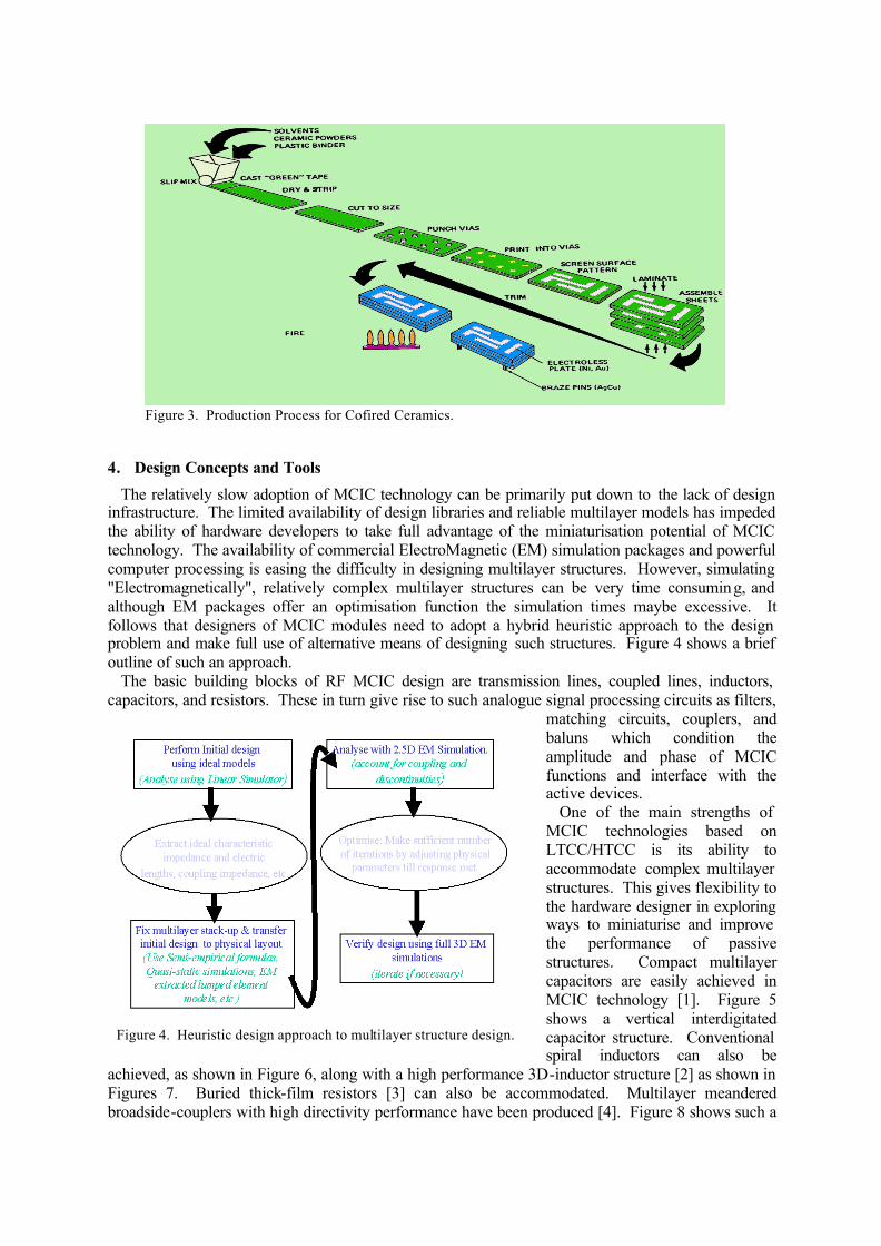
3. Cofired Ceramics Manufacturing Procedure
The manufacturing process for both LTCC and HTCC are very similar. Figure 3 shows the main stages of the process. The ceramic powder, organic binders and solvents are spread to the desired thickness and cut into correct size sheets (Green Tape). Via holes and component cavities are then punched into the tape using an automated punching tool, this is followed by the metalisation of via holes and conductors. Metalisation is accomplished using screen-printing of metal paste, which for HTCC is usually tungsten (or molybdenum), but LTCC can use the lowest resistivety conductors such as silver or copper. The layers are then assembled in order and laminated together. A burn of process to remove the solvents and organic binder follows this. For LTCC this takes place at 350 oC, whilst HTCC need to be placed under hydrostatic pressure in temperatures of about 500-600 oC. Finally, the whole LTCC structure is sintered at 850 oC for 15 minutes in air, whilst HTCC is sintered at 1350 oC for about 40 minutes in a gaseous atmosphere. LTCC uses ceramics based on glass compositions similar to those used in thick film dielectrics. HTCC for multilayer MCM applications typically uses 96% alumina.
Figure 2. Illustration of MCIC Scenario.
4. Design Concepts and Tools
The relatively slow adoption of MCIC technology can be primarily put down to the lack of design infrastructure. The limited availability of design libraries and reliable multilayer models has impeded the ability of hardware developers to take full advantage of the miniaturisation potential of MCIC technology. The availability of commercial ElectroMagnetic (EM) simulation packages and powerful computer processing is easing the difficulty in designing multilayer structures. However, simulating "Electromagnetically", relatively complex multilayer structures can be very time consuming, and although EM packages offer an optimisation function the simulation times maybe excessive. It follows that designers of MCIC modules need to adopt a hybrid heuristic approach to the design problem and make full use of alternative means of designing such structures. Figure 4 shows a brief outline of such an approach.
The basic building blocks of RF MCIC design are transmission lines, coupled lines, inductors, capacitors, and resistors. These in turn give rise to such analogue signal processing circuits as filters,
matching circuits, couplers, and baluns which condition the amplitude and phase of MCIC functions and interface with the active devices.
One of the main strengths of MCIC technologies based on LTCC/HTCC is its ability to accommodate complex multilayer structures. This gives flexibility to the hardware designer in exploring ways to miniaturise and improve the performance of passive structures. Compact multilayer capacitors are easily achieved in MCIC technology [1]. Figure 5 shows a vertical interdigitated capacitor structure. Conventional spiral inductors can also be
achieved, as shown in Figure 6, along with a high performance 3D-inductor structure [2] as shown in Figures 7. Buried thick-film resistors [3] can also be accommodated. Multilayer meandered broadside-couplers with high directivity performance have been produced [4]. Figure 8 shows such a
Figure 3. Production Process for Cofired Ceramics.
Figure 4. Heuristic design approach to multilayer structure design.
structure. This structure is a compensated broadside-coupler with capacitors to ground [5] implemented as parallel plate capacitors.
In the last few years the number of reported results of LTCC based modules has risen. As an example, Reference [6] reports on the results of a comparison between a CMOS power amplifier implemented with passives integrated on the RFIC chip, passives implemented as discrete surface mount, and with passives implemented in LTCC, for bluetooth applications. The paper concludes that efficiency and output power level performance was improved by the implementation of high Q passives in LTCC.
5. Conclusion
The demand for higher performance systems that are smaller and have the potential to be more cost effective has lead hardware designers to adopt new approaches. In this paper we have presented the MCIC concept which shows good promise for many applications. The MCIC technology approach enables passives to be embedded in a packaging substrate such as LTCC, while accommodating a multiplicity of monolithic IC technologies.
6. References
[1] W. Blood, Feng Ling, T. Myers, M. Petros. “Library Development Process for Embedded Capacitors in LTCC”; IEEE Conf. EPEP 2000, Pages 147-150.
[2] A. Sutono, A. Pham, J. Laskar, W.R. Smith. “Development of Three Dimensional Ceramic -Based MCM Inductors for Hybrid RF/Microwave Applications”; IEEE RFIC-S 1999, Pages 175-178.
[3] K. Delaney, J. Barrett, J. Barton, R. Doyle. “Characterization and Performance Prediction for Integral Resistors in Low Temperature Cofired Ceramic Technology”; IEEE Trans. Advanced Packaging, Vol. 22, No.1, Feb. 1999, Pages 78-85.
[4] S. Al-Taei, P. Lane, G. Passiopoulos. “Design of High Directivity Directional Couplers in Multilayer Ceramic Technologies”; IEEE MTT-S 2001.
[5] International Patent application files on 02.28.2001. application number PCT/EP01/02249. [6] Y.J.E. Chen, M.Hamai, D. Heo, A. Sutono, S. Yoo, and J. Laskar. “RF Power Amplifier
Integration in CMOS Technology”; IEEE MTT-S Digest 2000, Pages 545-548.
Figure 5. 3D vertical Interdigitated Capacitor in LTCC-MCIC Technology
Figure 6. Conventional Grounded Spiral Inductor in LTCC-MCIC Technology
Figure 7. Multilayer Vertical Spiral Inductor in LTCC-MCIC Technology
Figure 8. Multilayer High Directivity Broadside coupler


![BLF881; BLF881S · C1, C2 multilayer ceramic chip capacitor 5.1 pF [1] C3, C4 multilayer ceramic chip capacitor 10 pF [2] C5 multilayer ceramic chip capacitor 6.8 pF [1] C6 multilayer](https://static.documents.pub/doc/80x56/5ceec0d888c99376408beb1c/blf881-blf881s-c1-c2-multilayer-ceramic-chip-capacitor-51-pf-1-c3-c4-multilayer.jpg)


