YANG ET AL. VOL. XXX ’ NO. XX ’ 000–000 ’ XXXX www.acsnano.org A C XXXX American Chemical Society Multilayer Transparent Top Electrode for Solution Processed Perovskite/Cu(In,Ga)(Se,S) 2 Four Terminal Tandem Solar Cells Yang (Michael) Yang, †,§ Qi Chen, †,‡,§ Yao-Tsung Hsieh, †,‡ Tze-Bin Song, †,‡ Nicholas De Marco, †,‡ Huanping Zhou, * ,†,‡ and Yang Yang * ,†,‡ † Department of Materials Science and Engineering, University of California, Los Angeles, California 90095, United States and ‡ California NanoSystems Institute, University of California, Los Angeles, California 90095, United States. § These authors contributed equally to this work. S unlight is one of the most abundant renewable energy sources on our planet, yet it remains poorly utilized. Over the past decades, people have sought alternative materials for photovoltaic devices that feature both low cost and high efficiency, e.g., organic photovoltaics (OPV), 16 Dye Sensitized Solar Cells (DSSC), 710 etc. The recent advent of the organicinorganic hybrid halide perovskite (PVSK) has led to rapid progress of photo- voltaic/optoelectronic devices. 1125 In ad- dition, the capability for the simple film deposition through either vacuum or solution- based methods makes it a tremendous candi- date for the future solar cell market. As the efficiency of the PVSK solar cell is approaching its theoretical limitation, it is necessary to start to consider how to go beyond the S-Q limit. There are two major losses that currently prevent a higher PCE from being obtained in single junction PVSK devices in (1) the below band gap transmis- sion and (2) the thermal relaxation of hot charge carriers. The band gap of semicon- ductors can be reduced to enhance absorp- tion and increase the short circuit current (J sc ), while the ultrafast hot carrier relaxation process sets the limit of the open circuit voltage (V oc ) to be the band gap. The most promising method to circumvent both effects is to construct a tandem junction device consisting of a bottom cell fabricated based on prevailing solar cell techniques e.g., Si and CIGS, and a top cell with a higher bandgap absorber. Up to date, this method has had limited success due to the absence of suitable materials to produce high efficiency top cells compatible with current photovoltaic (PV) technology as bottom cells. The rapid pro- gress of the organicinorganic hybrid pe- rovskite materials with ∼1.55 eV band gap is a potential candidate to be utilized as the top cell to further improve the state-of-the-art of the solar cell technology. This family of ma- terials is gifted the most attractive optoelec- tronic characteristics as an ideal standalone * Address correspondence to [email protected], [email protected]. Received for review May 27, 2015 and accepted June 21, 2015. Published online 10.1021/acsnano.5b03189 ABSTRACT Halide perovskites (PVSK) have attracted much attention in recent years due to their high potential as a next generation solar cell material. To further improve perovskites progress toward a state-of-the-art technology, it is desirable to create a tandem structure in which perovskite may be stacked with a current prevailing solar cell such as silicon (Si) or Cu(In,Ga)(Se,S) 2 (CIGS). The transparent top electrode is one of the key components as well as challenges to realize such tandem structure. Herein, we develop a multilayer transparent top electrode for perovskite photovoltaic devices delivering an 11.5% efficiency in top illumination mode. The transparent electrode is based on a dielectric/metal/dielectric structure, featuring an ultrathin gold seeded silver layer. A four terminal tandem solar cell employing solution processed CIGS and perovskite cells is also demonstrated with over 15% efficiency. KEYWORDS: perovskite . transparent electrode . tandem . dielectric/metal/dielectric . solar cell ARTICLE
Transcript
YANG ET AL. VOL. XXX ’ NO. XX ’ 000–000 ’ XXXX
www.acsnano.org
A
CXXXX American Chemical Society
Multilayer Transparent TopElectrode for Solution ProcessedPerovskite/Cu(In,Ga)(Se,S)2 FourTerminal Tandem Solar CellsYang (Michael) Yang,†,§ Qi Chen,†,‡,§ Yao-Tsung Hsieh,†,‡ Tze-Bin Song,†,‡ Nicholas De Marco,†,‡
Huanping Zhou,*,†,‡ and Yang Yang*,†,‡
†Department of Materials Science and Engineering, University of California, Los Angeles, California 90095, United States and ‡California NanoSystems Institute,University of California, Los Angeles, California 90095, United States. §These authors contributed equally to this work.
Sunlight is one of the most abundantrenewable energy sources on our planet,yet it remains poorly utilized. Over the
past decades, people have sought alternativematerials forphotovoltaicdevices that featureboth lowcost andhighefficiency, e.g., organicphotovoltaics (OPV),1�6 Dye Sensitized SolarCells (DSSC),7�10 etc. The recent advent of theorganic�inorganic hybrid halide perovskite(PVSK) has led to rapid progress of photo-voltaic/optoelectronic devices.11�25 In ad-dition, the capability for the simple filmdeposition througheither vacuumor solution-basedmethodsmakes it a tremendous candi-date for the future solar cell market.As the efficiency of the PVSK solar cell
is approaching its theoretical limitation, it isnecessary to start to consider how to gobeyond the S-Q limit. There are two majorlosses that currently prevent a higher PCEfrom being obtained in single junction PVSKdevices in (1) the below band gap transmis-sion and (2) the thermal relaxation of hot
charge carriers. The band gap of semicon-ductors can be reduced to enhance absorp-tion and increase the short circuit current(Jsc), while the ultrafast hot carrier relaxationprocess sets the limit of the open circuitvoltage (Voc) to be the band gap. The mostpromisingmethod to circumvent both effectsis to construct a tandem junction deviceconsisting of a bottom cell fabricated basedon prevailing solar cell techniques e.g., Si andCIGS, and a top cell with a higher bandgapabsorber. Up to date, this method has hadlimited success due to the absence of suitablematerials to produce high efficiency top cellscompatible with current photovoltaic (PV)technology as bottom cells. The rapid pro-gress of the organic�inorganic hybrid pe-rovskite materials with∼1.55 eV band gap isa potential candidate to beutilized as the topcell to further improve the state-of-the-art ofthe solar cell technology. This family of ma-terials is gifted the most attractive optoelec-tronic characteristics as an ideal standalone
Received for review May 27, 2015and accepted June 21, 2015.
Published online10.1021/acsnano.5b03189
ABSTRACT Halide perovskites (PVSK) have attracted much attention in recent years due to
their high potential as a next generation solar cell material. To further improve perovskites
progress toward a state-of-the-art technology, it is desirable to create a tandem structure in which
perovskite may be stacked with a current prevailing solar cell such as silicon (Si) or Cu(In,Ga)(Se,S)2(CIGS). The transparent top electrode is one of the key components as well as challenges to realize
such tandem structure. Herein, we develop a multilayer transparent top electrode for perovskite
photovoltaic devices delivering an 11.5% efficiency in top illumination mode. The transparent
electrode is based on a dielectric/metal/dielectric structure, featuring an ultrathin gold seeded
silver layer. A four terminal tandem solar cell employing solution processed CIGS and perovskite
cells is also demonstrated with over 15% efficiency.
absorber, including a high absorption coefficient, tun-ablebandgap, longcarrier diffusion lengthandmore.20,26
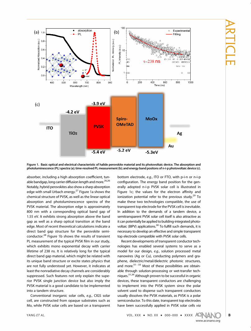
Notably, hybrid perovskites also showa sharp absorptionedge with small Urbach energy.27 Figure 1a shows thechemical structure of PVSK, as well as the linear opticalabsorption and photoluminescence spectra of thePVSK material. The absorption edge is approximately800 nm with a corresponding optical band gap of1.55 eV. It exhibits strong absorption above the bandgap as well as a sharp optical transition at the bandedge. Most of recent theoretical calculations indicate adirect band gap structure for the perovskite semi-conductor.28 Figure 1b shows the results of transientPL measurement of the typical PVSK film in our study,which exhibits mono exponential decay with carrierlifetime of 238 ns. It is relatively long for the typicaldirect band gap material, which might be related withits unique band structure or excite states physics thatare not fully understood yet. However, it indicates atleast the nonradiative decay channels are considerablysuppressed. Such features not only explain the supe-rior PVSK single junction device but also imply thePVSK material is a good candidate to be implementedinto a tandem structure.Conventional inorganic solar cells, e.g., CIGS solar
cell, are constructed from opaque substrates such asMo, while PVSK solar cells are based on a transparent
bottom electrode, e.g., ITO or FTO, with p-i-n or n-i-pconfiguration. The energy band position for the gen-erally adopted n-i-p PVSK solar cell is illustrated inFigure 1c; the values for the electron affinity andionization potential refer to the previous study.29 Tomake these two technologies compatible, the use oftransparent top electrode for the PVSK cell is inevitable.In addition to the demands of a tandem device, asemitransparent PVSK solar cell itself is also attractive asit canpotentiallybeapplied tobuilding-integratedphoto-voltaic (BIPV) applications.30 To fulfill such demands, it isnecessary to develop an effective and simple transparenttop electrode compatible with PVSK solar cells.Recent developments of transparent conductor tech-
nologies has enabled several systems to serve as amodel for our design, e.g., solution processed metalnanowires (Ag or Cu), conducting polymers and gra-phene, dielectric/metal/dielectric photonic structures,and more.31�33 Most of these possibilities are obtain-able through solution-processing or wet-transfer tech-niques.31,34 Although proven to be successful in organicdevices, these transparent conductors are challengingto implement into the PVSK system since the polarsolvent used to disperse such transparent conductorsusually dissolves the PVSK materials, as PVSK is a polarsemiconductor. To this date, transparent top electrodeshave been successfully applied in PVSK solar cells via
Figure 1. Basic optical and electrical characteristic of halide perovskite material and its photovoltaic device. The absorption andphotoluminescence (PL) spectra (a); time-resolvedPLmeasurement (b); and energybandpositons of n-i-p photovoltaic device (c).
ARTIC
LE
YANG ET AL. VOL. XXX ’ NO. XX ’ 000–000 ’ XXXX
www.acsnano.org
C
a limited number of approaches. A thin gold layer(∼10 nm) has been reported via thermal evaporationto achieve a device PCE of 7.5%.35 In another report,a transparent conducting adhesive was utilized tolaminate a Ni mesh embedded within PET onto theperovskite solar cell to yield a decent PCE over 15%.36
The development of a dielectric/metal/dielectric(DMD) (MoOx/Ag/MoOx) structure as the semitrans-parent top electrode offers a compelling approachfor the pursuit of a semitransparent PVSK top cell. Asmentioned previously, PVSK materials and adjacenttransport materials are chemically and mechanicallyunstable for the direct implication of solution pro-cessed top electrodes, e.g., Ag NWs, carbon nanotubes,or sputtered metal oxides. In addition, deposition ofDMD structures is based on simple thermal evapora-tion processes, which appear to be a cost-effectiveapproach in comparison to the combined techniquesof thermal evaporation of a buffer layer followed bysputtering of a metal oxide. Apart from the ease ofprocessing, this method provides for judicious controlover film thickness of eachmaterial to ensure reproduc-ibility of the resulting device performance.
RESULTS AND DISCUSSION
This PVSK device employs the widely used n-i-pplanar structure with compact TiO2 as the electrontransport layer (ETL), and Spiro-OMeTAD as the holetransport layer (HTL). Processing of the TiO2 film wasachieved at 150 �C, which is a rather low temperaturefor compact ETL materials. The PVSK layer is depositedon the top of TiO2 through a two-step solution-processing technique, the details of which are includedin the Methods section; the film morphology is givenin Supporting Information Figure S1. Spiro-OMeTADwith ∼350 nm thickness was subsequently deposited,serving as the HTL. We used thermally evaporatedMoOx as the dielectric material in the DMD structuredue to the hole conducting nature and suitable bandposition of MoOx compatible with Spiro-OMeTAD toprovide for efficient hole extraction and transport. Theband position of each layer is illustrated in Figure 1c.MoOx is a commonly used hole transportingmaterial inorganic photovoltaic devices and silicon solar cell.37,38
In this study, we also confirms that the Spiro-OMeTAD/MoOx layer work as an effective hole selective layer.The device parameters of this type of device are almostcomparable with the typical Spiro-OMeTAD/Au device,as shown in Supporting Information Figure S2. Inaddition, we also find that theMoOxmetal oxide affectsthe surface properties of the original Spiro-OMeTADhole transport materials, providing improved adhe-sion for the following metal deposition. The entiretop electrode is then completed by subsequent de-position of a thin metal layer and an additional MoOx
dielectric layer for optical interference to enhance thetransparency. The metal film has strong reflection even
at 11 nm thickness; the top MoOx layer can be consid-ered as the antireflection layer. However, it is challen-ging to achieve antireflection for thewhole spectra, andhence, the optimal thickness of this layer depends onparticular photovoltaic system.The most crucial part of the transparent electrode
is the metal layer stacking in-between the dielectricmaterials, which determines the trade-off between thetransparency and the conductivity of the entire topelectrode. Most traditional DMD structures employ asilver, and occasionally gold, middle layer.39�41 Weinitially used a thin Ag layer, due to its high visibletransparence and low cost. The silver thin film depos-ited on the dielectric material is likely to form isolatedclusters for the initial few nanometers of deposition.Therefore, the percolation thickness (thickness atwhich the film becomes continuous) of silver mustexceed the threshold, where the following coalescenceand film growth process can be completed to form acontinuous network. Attempts to improve film qualityduring metal deposition consider not only film thick-ness, but other deposition parameters as well. Forinstance, on the basis of the fast evaporation rate(>5 nm/s) of silver, a more continuous film with higherconductivity at a similar range of film thickness can beachieved. This is likely due to the rather sufficientnumber of vapor atoms or molecules that condenseandmerge together to establish a continuous networkon the substrate. However, in PVSK solar cells, such afast deposition rate can easily damage the Spiro-OMeTAD and even the PVSK film. In addition, substratetemperature and roughness have also been found toplay an important role in certain circumstances, whichincreases the complexity of this technology and re-duces the device performance, yield and reproducibil-ity. In our case, it is desirable to achieve Ag filmpercolation thicknesses as low as possible using a milddeposition method, so as to minimize optical lossesfrom absorption by the electrode itself.Interestingly, we found that in an ultrathin gold seed
layer (∼1 nm) beneath a silver film provides an idealsolution for improving the adhesion and reducing thepercolation thickness of the metal film sandwichedbetween the dielectric structures. This results in adramatic change of silver film morphology. As shownin Figure (2a�c), without gold seed layer, the silver filmis not continuous at 11 nm, presenting isolated metalinlands, and the film is highly resistive. With the samemetal film thickness, it becomes continuous acrossthe entire film by inserting only 1 nm gold seed layeras shown in Figure 2b. In contrast, the pure gold thinfilm with same thickness also shows noncontinuousfeature, the film consists of tiny isolated gold islandsas shown in Figure 2c. This result suggests that asubstantially different nucleation and growth modeof the metal film occurs during the evaporation pro-cess by incorporating alternative gold seeding layer.
ARTIC
LE
YANG ET AL. VOL. XXX ’ NO. XX ’ 000–000 ’ XXXX
www.acsnano.org
D
Generally, in case of metal films nucleation, the ada-toms tend to bound to each other instead of boundingto the substrates, and therefore, they grow via Volmer�Weber (island) mode. It explains the noncontinuousfilm appearing in both cases of the individual Au andAg deposition below the critical thickness. While animproved wetting of the substrate has proven to befavorable for the Frank�van der Merwe (layer-by-layer)growth, it is the reason for the widely used “trick” that Crseed is predeposited before the subsequent Au deposi-tion in many electric devices. In our study, the gold ispredeposited on the substrate and form islands, thesubsequent adsorbed Ag atoms/molecules (adatoms)may have the chance to be more strongly bound to thesubstrate than to the nearby gold islands. The interac-tion between Ag and substrate is energetically morefavorable than the Ag�Au interaction, since gold hashigher surface energy. The growth mode transitionsfrom Volmer�Weber (island) mode in homogeneousAg or Au thin film to the Frank�van der Merwe (layer-by-layer) mode in the Au/Ag heterostructure thin film.Facilitated by the gold seed, the silver film with only10 nm result in a continuous film, and such a smallpercolation thickness will ensure good optical transpar-ency aswell as the conductivity of the thinfilmelectrode.As shown in Figure 2d, the conductivity of the
corresponding silver film improves several orders ofmagnitude from 20KΩ/0 (11 nmAg) to around 16Ω/0(1 nm Auþ 10 nm Ag). This is presumably because the
isolated metal islands are well connected to formcharge conduction pathways. The gold seeded silverfilm is also superior when compared to the pure goldfilm in terms of conductivity and transparency, wherethe same thickness of gold is very resistive and exhibitslow transmittance in the visible region due to thestrong plasmonic scattering effect of the gold nanodomains.42 A dielectric toping layer was used to furtherimprove the transmittance of the electrode. All thedielectric materials in principle can serve this functionso long as they possess a large band gap to avoidoptical absorption (e.g., LiF).35 Here, we employ MoOx
as the top layer due to its ease of processing, withoutchanging the thermal evaporation source. The trans-mittance spectrum can be tuned by different MoOx
thicknesses to match the absorption spectra of theactive layer, as shown in Figure 2e. The final optimizedparameters of this D/M/D transparent top electrode isillustrated in Figure 2f. The transmittance is particularlyhigh from 550 to 800 nm, within which the PVSKmaterial actively absorbs photons.The architecture of the top illuminated semitrans-
parent PVSK solar cell as well as the cross-sectionimage of each layer are shown in Figure 3a. The IVcurve of the optimized championing device is shown inFigure 3b, delivering a very good device performanceof 11.5% power conversion efficiency (PCE). As areference, the “regular” PVSK solar cell with Spiro-OMeTAD as hole transporting layer and ∼100 nm Au
Figure 2. Characterization of multilayer transparent top electrode. The film morphology of pristine silver (a), gold seededsilver (b) and pristine gold (c) layer with same metal thickness; the transparence and conductivity of pristine silver, goldseeded silver, and pristine gold film (d); the transparency of the multilayer electrode with different MoOx topping layerthickness (e); the optimized parameters for the multilayer transparent electrode used in PVSK solar cell (f).
ARTIC
LE
YANG ET AL. VOL. XXX ’ NO. XX ’ 000–000 ’ XXXX
www.acsnano.org
E
electrode is also fabricated and shows average powerconversion efficiency of ∼16.5%; the IV curve of thetypical PVSK solar cell with regular electrode is in-cluded in Supporting Information Figure S2. The fillfactor (FF) of the top illuminated PVSK cell achieves75%, which is comparable to the best performing PVSKsolar cells made with regular metal electrodes. Thedevice performance distribution is given in Figure 3c.The open circuit voltage (Voc) reached as high as 1.05 V.This is also a reasonably high value considering that thephotoinduced excess carrier concentration inside thesemitransparent PVSK is slightly lower than that ofPVSK in regular devices, so that the quasi Fermi levelsplitting is slightly reduced. The high FF and Voc bothindicate that the sheet resistance of this D/M/D trans-parent electrode is low enough to avoid the resistivelosses. The short circuit current (Jsc) is lower than that inthe regular device due to the transmittance loss fromthe top electrode, achieving a value of 14.6 mA/cm2,which is approximately 70% of that seen in typicalPVSK photovoltaic devices. Such photocurrent loss cor-relates with the overall transmittance of the D/M/Dtransparent electrode.
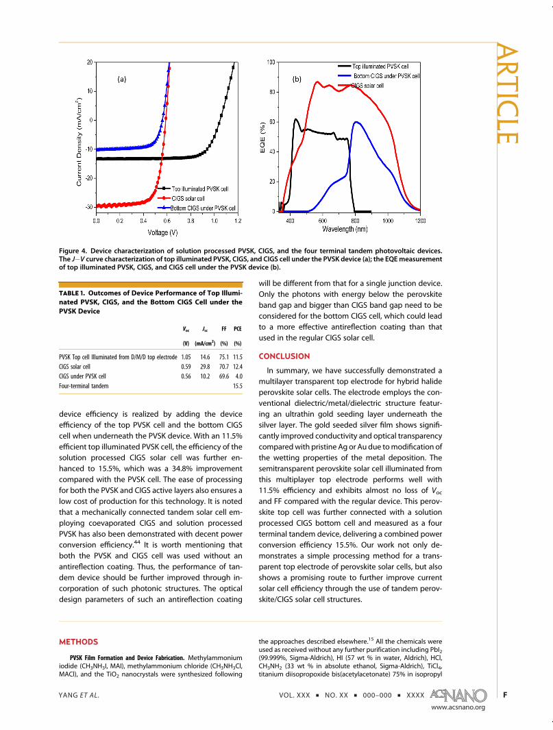
On the basis of this D/M/D transparent top electrode,a four-terminal tandem solar cell employing a solutionprocessed CIGS bottom cell was also demonstrated.The CIGS bottom cell was obtained following previousprocedures,43 andyields aVoc of 0.59V, Jsc of 29.8mA/cm2,FF of 70.7% and overall PCE of 12.4%. It must be notedthat the top and bottom cell should have an approxi-mately equal PCE in order to maximize the benefit ofusing a tandem device instead of a single junction.Hence, solution processed CIGS bottom cells and PVSKtop cells are believed to be a good combination for atandem structure. The four terminal device configura-tion is shown in Supporting Information Figure S3, thedevice is illuminated from the D/M/D electrode, andthe IV curve of top and bottom cell were measuredseparately. The CIGS bottom cell underneath the topcell shows an efficiency of 4.0%, with Jsc of 10.2mA/cm2,Voc of 0.56 V and FF of 69.6%. The current�voltagecurves and the external quantum efficiency (EQE)curves of the top PVSK cell, unfiltered CIGS solar cell,and CIGS bottom cell underneath the PVSK cell areshown in Figure 4a,b. All corresponding device param-eters are included in Table 1. The four-terminal tandem
Figure 3. Device structure and performance of top illuminated PVSK solar cell. The schematic and TEM cross-sectional imageof the photovoltaic device (a); J�V curve of the optimized device (b); the statistic of the device efficiency (c).
ARTIC
LE
YANG ET AL. VOL. XXX ’ NO. XX ’ 000–000 ’ XXXX
www.acsnano.org
F
device efficiency is realized by adding the deviceefficiency of the top PVSK cell and the bottom CIGScell when underneath the PVSK device. With an 11.5%efficient top illuminated PVSK cell, the efficiency of thesolution processed CIGS solar cell was further en-hanced to 15.5%, which was a 34.8% improvementcompared with the PVSK cell. The ease of processingfor both the PVSK and CIGS active layers also ensures alow cost of production for this technology. It is notedthat a mechanically connected tandem solar cell em-ploying coevaporated CIGS and solution processedPVSK has also been demonstrated with decent powerconversion efficiency.44 It is worth mentioning thatboth the PVSK and CIGS cell was used without anantireflection coating. Thus, the performance of tan-dem device should be further improved through in-corporation of such photonic structures. The opticaldesign parameters of such an antireflection coating
will be different from that for a single junction device.Only the photons with energy below the perovskiteband gap and bigger than CIGS band gap need to beconsidered for the bottom CIGS cell, which could leadto a more effective antireflection coating than thatused in the regular CIGS solar cell.
CONCLUSION
In summary, we have successfully demonstrated amultilayer transparent top electrode for hybrid halideperovskite solar cells. The electrode employs the con-ventional dielectric/metal/dielectric structure featur-ing an ultrathin gold seeding layer underneath thesilver layer. The gold seeded silver film shows signifi-cantly improved conductivity and optical transparencycomparedwith pristine Ag or Au due tomodification ofthe wetting properties of the metal deposition. Thesemitransparent perovskite solar cell illuminated fromthis multiplayer top electrode performs well with11.5% efficiency and exhibits almost no loss of Vocand FF compared with the regular device. This perov-skite top cell was further connected with a solutionprocessed CIGS bottom cell and measured as a fourterminal tandem device, delivering a combined powerconversion efficiency 15.5%. Our work not only de-monstrates a simple processing method for a trans-parent top electrode of perovskite solar cells, but alsoshows a promising route to further improve currentsolar cell efficiency through the use of tandem perov-skite/CIGS solar cell structures.
METHODS
PVSK Film Formation and Device Fabrication. Methylammoniumiodide (CH3NH3I, MAI), methylammonium chloride (CH3NH3Cl,MACl), and the TiO2 nanocrystals were synthesized following
the approaches described elsewhere.15 All the chemicals wereused as received without any further purification including PbI2(99.999%, Sigma-Aldrich), HI (57 wt % in water, Aldrich), HCl,CH3NH2 (33 wt % in absolute ethanol, Sigma-Aldrich), TiCl4,titanium diisopropoxide bis(acetylacetonate) 75% in isopropyl
Figure 4. Device characterization of solution processed PVSK, CIGS, and the four terminal tandem photovoltaic devices.The J�V curve characterization of top illuminated PVSK, CIGS, and CIGS cell under the PVSK device (a); the EQEmeasurementof top illuminated PVSK, CIGS, and CIGS cell under the PVSK device (b).
TABLE 1. Outcomes of Device Performance of Top Illumi-
nated PVSK, CIGS, and the Bottom CIGS Cell under the
PVSK Device
Voc Jsc FF PCE
(V) (mA/cm2) (%) (%)
PVSK Top cell Illuminated from D/M/D top electrode 1.05 14.6 75.1 11.5CIGS solar cell 0.59 29.8 70.7 12.4CIGS under PVSK cell 0.56 10.2 69.6 4.0Four-terminal tandem 15.5
ARTIC
LE
YANG ET AL. VOL. XXX ’ NO. XX ’ 000–000 ’ XXXX
www.acsnano.org
G
alcohol (TiAcac, Sigma-Aldrich), spiro-OMeTAD (Lumtec), di-methylformamide (DMF), Li-bis(trifluoromethanesulfonyl) imide(Li-TFSI, Sigma), diethyl ether, acetone, isopropyl alcohol, ace-tonitrile, ethanol, 2-methoxyethanol, and benzyl alcohol. ITO orglass substrates (for PL measurements) were sequentiallywashed with isopropyl alcohol, acetone, distilled water andethanol. The ETL was subsequently coated on ITO substrateswith a TiAcac stabilized TiO2 solution and annealed at 150 �C for30 min in air. PbI2 (dissolved in DMF, 400 mg/mL) was spin-coated on top of ITO/TiO2 substrate at 2500 rpm for 30 s. Thendissolved in 2-propanol, a mixture of MAI/MACl (50 mg/mL,5mg/mL) was spin-coated on top of the dried PbI2 layer at roomtemperature at 2000 rpm for 30 s in the dry air (at Dew Pointof�70 �C). All of the films were annealed in the air at 135 �C fordesired time. A hole transport layer (HTL) solution was coatedon the perovskite film at 3000 rpm for 30 s, where a spiro-OMeTAD/chlorobenzene (90 mg/1 mL) solution was employedwith addition of 45 μL of Li-TFSI/acetonitrile (170 mg/1 mL) and10 μL of tBP. Finally, the counter electrode was deposited bythermal evaporation of gold under a pressure of 5� 10�5 Torr.The active area was 0.108 cm2. The as-fabricated referencedevice depicts from the bottom to the top, the 150 nm thickITO electrode, 40 nm of TiO2, 350 nm of perovskite, 200 nm ofspiro-OMeTAD, and 100 nm of gold. The fabrication of solutionprocessed CIGS solar cell follows previous work demonstratedin this study.43 The transparent top electrode based deviceadopts all the device fabrication parameters as the referencedevice except replacing the Au electrode by multilayer topelectrodes. The MoOx/Au/Ag/MoOx multilayer top electrode isdeposited subsequently with thermal evaporation method,with the thickness of 10, 1, 10, and 40 nm, respectively. Theevaporation rates for each layer are 0.1, 0.02, 0.1, and 0.1 nm/s,respectively.
Optical Characterization. The absorptions of different transpar-ent electrodes and the PVSK film are measured with HitachiUV�vis spectrometer in the transmission mode. The PL mea-surement is conducted with HORIBA fluorescence spectro-meter, and the transient PL is measured using PicoQuant timecorrelated single photon counter.
Device Measurement. The current�voltage (J�V) measure-ments of the photovoltaic devices were conducted using aKeithley 236 Source-Measure unit. A xenon lamp with anAM1.5G filter (NEWPORT) simulated 1 sun conditions, and thelight intensity at the sample was 100mW/cm2, calibrated with aMono-Si photodiode with KG-5 color filter. The reference diodeis traceable to NREL certification. EQE measurements wereconducted with an integrated EQE system from EnliTech. Asfor the four�terminal tandem device, the top PVSK solar cell ismeasured using the same setup while the device is illuminatedfrom the top DMD electrode; the bottom CIGS solar cell ismeasured with top PVSK device as the filter.
Conflict of Interest: The authors declare no competingfinancial interest.
Acknowledgment. This work was financially supported bythe National Science Foundation (NSF-ECCS 1202231, ProgramManager: Dr. Paul Werbos), Air Force Office of ScientificResearch (Grant No. FA9550-12-1-0074, Program Manager:Dr. C. Lee). We also thank the technical support and discussionsfrom Mr. Chun-Chiang Kuo, Dr. Jingbi You, Dr. Ziruo Hong, Dr.Gang Li, and Mr. Lei Meng.
Supporting Information Available: SEM image of the PVSKfilm on top of TiO2; IV curves of the regular PVSK solar cell;Device stacking schematic for the four-terminal tandem device.The Supporting Information is available free of charge on theACS Publications website at DOI: 10.1021/acsnano.5b03189.
REFERENCES AND NOTES1. Li, G.; Zhu, R.; Yang, Y. Polymer Solar Cells. Nat. Photonics
2012, 6, 153–161.2. Li, Y. Molecular Design of Photovoltaic Materials for Poly-
mer Solar Cells: Toward Suitable Electronic Energy Levelsand Broad Absorption. Acc. Chem. Res. 2012, 45, 723–733.
3. Liang, Y.; Yu, L. A New Class of Semiconducting Polymersfor Bulk Heterojunction Solar Cells with Exceptionally HighPerformance. Acc. Chem. Res. 2010, 43, 1227–1236.
4. Li, G.; Shrotriya, V.; Huang, J.; Yao, Y.; Moriarty, T.; Emery, K.;Yang, Y. High-Efficiency Solution Processable PolymerPhotovoltaic Cells by Self-Organization of Polymer Blends.Nat. Mater. 2005, 4, 864–868.
6. You, J.; Dou, L.; Yoshimura, K.; Kato, T.; Ohya, K.; Moriarty, T.;Emery, K.; Chen, C.-C.; Gao, J.; Li, G.; Yang, Y. A PolymerTandem Solar Cell with 10.6% Power Conversion Effi-ciency. Nat. Commun. 2013, 4, 1446.
7. Chung, I.; Lee, B.; He, J.; Chang, R. P. H.; Kanatzidis, M. G.All-Solid-State Dye-Sensitized Solar Cells with High Effi-ciency. Nature 2012, 485, 486–489.
8. Daeneke, T.; Kwon, T.-H.; Holmes, A. B.; Duffy, N. W.; Bach,U.; Spiccia, L. High-Efficiency Dye-Sensitized Solar Cellswith Ferrocene-Based Electrolytes. Nat. Chem. 2011, 3,211–215.
9. Grätzel, M. Recent Advances in Sensitized MesoscopicSolar Cells. Acc. Chem. Res. 2009, 42, 1788–1798.
10. Wang, M.; Chamberland, N.; Breau, L.; Moser, J.-E.;Humphry-Baker, R.; Marsan, B.; Zakeeruddin, S. M.; Grätzel,M. An Organic Redox Electrolyte to Rival Triiodide/Iodidein Dye-Sensitized Solar Cells. Nat. Chem. 2010, 2, 385–389.
11. Green, M. A.; Ho-Baillie, A.; Snaith, H. J. The Emergence ofPerovskite Solar Cells. Nat. Photonics 2014, 8, 506–514.
12. Heo, J. H.; Im, S. H.; Noh, J. H.; Mandal, T. N.; Lim, C.-S.;Chang, J. A.; Lee, Y. H.; Kim, H.-j.; Sarkar, A.; NazeeruddinMd,K.; et al. Efficient Inorganic-Organic Hybrid Heterojunc-tion Solar Cells Containing Perovskite Compound andPolymeric Hole Conductors. Nat. Photonics 2013, 7, 486–491.
13. Lin, Q.; Armin, A.; Nagiri, R. C. R.; Burn, P. L.; Meredith, P.Electro-Optics of Perovskite Solar Cells. Nat. Photonics2015, 9, 106–112.
14. Liu, D.; Kelly, T. L. Perovskite Solar Cells with a PlanarHeterojunction Structure Prepared Using Room-Tempera-ture Solution Processing Techniques. Nat. Photonics 2014,8, 133–138.
15. Liu, M.; Johnston, M. B.; Snaith, H. J. Efficient PlanarHeterojunction Perovskite Solar Cells by Vapour Deposi-tion. Nature 2013, 501, 395–398.
16. Park, N.-G. Organometal Perovskite Light AbsorbersToward a 20% Efficiency Low-Cost Solid-State MesoscopicSolar Cell. J. Phys. Chem. Lett. 2013, 4, 2423–2429.
24. Song, T.-B.; Chen, Q.; Zhou, H.; Luo, S.; Yang, Y.; You, J.;Yang, Y. Unraveling Film Transformations and DevicePerformance of Planar Perovskite Solar Cells. Nano Energy2015, 12, 494–500.
25. Song, T.-B.; Chen,Q.; Zhou, H.; Jiang, C.;Wang,H.-H.; Yang, Y.;Liu, Y.; You, J.; Yang, Y. Perovskite Solar Cells: Film Formationand Properties. J. Mater. Chem. A 2015, 3, 9032–9050.
26. Xing, G.; Mathews, N.; Lim, S. S.; Yantara, N.; Liu, X.; Sabba,D.; Grätzel, M.; Mhaisalkar, S.; Sum, T. C. Low-TemperatureSolution-Processed Wavelength-Tunable Perovskites forLasing. Nat. Mater. 2014, 13, 476–480.
27. De Wolf, S.; Holovsky, J.; Moon, S.-J.; Löper, P.; Niesen, B.;Ledinsky, M.; Haug, F.-J.; Yum, J.-H.; Ballif, C. Organome-tallic Halide Perovskites: Sharp Optical Absorption Edgeand Its Relation to Photovoltaic Performance. J. Phys.Chem. Lett. 2014, 5, 1035–1039.
28. Umari, P.; Mosconi, E.; De Angelis, F. Relativistic GWCalculations on CH3NH3PbI3 and CH3NH3SnI3 Perovskitesfor Solar Cell Applications. Sci. Rep. 2014, 4, No. 4467.
29. Gao, P.; Gratzel, M.; Nazeeruddin, M. K. Organohalide LeadPerovskites for Photovoltaic Applications. Energy Environ.Sci. 2014, 7, 2448–2463.
30. Eperon, G. E.; Burlakov, V. M.; Goriely, A.; Snaith, H. J.Neutral Color Semitransparent Microstructured PerovskiteSolar Cells. ACS Nano 2014, 8, 591–598.
31. Wu, H.; Kong, D.; Ruan, Z.; Hsu, P.-C.; Wang, S.; Yu, Z.;Carney, T. J.; Hu, L.; Fan, S.; Cui, Y. A Transparent ElectrodeBased on a Metal Nanotrough Network. Nat. Nanotechnol.2013, 8, 421–425.
32. Mao, L.; Chen, Q.; Li, Y.; Li, Y.; Cai, J.; Su, W.; Bai, S.; Jin, Y.; Ma,C.-Q.; Cui, Z.; et al. Flexible Silver Grid/PEDOT:PSS HybridElectrodes for Large Area Inverted Polymer Solar Cells.Nano Energy 2014, 10, 259–267.
33. Li, Y.; Mao, L.; Gao, Y.; Zhang, P.; Li, C.; Ma, C.; Tu, Y.; Cui, Z.;Chen, L. ITO-FreePhotovoltaicCellUtilizingaHigh-SesolutionSilver Grid Current Collecting Layer. Sol. Energy Mater. Sol.Cells 2013, 113, 85–89.
35. Roldan-Carmona, C.; Malinkiewicz, O.; Betancur, R.; Longo,G.; Momblona, C.; Jaramillo, F.; Camacho, L.; Bolink, H. J.High Efficiency Single-Junction Semitransparent Perov-skite Solar Cells. Energy Environ. Sci. 2014, 7, 2968–2973.
36. Bryant, D.; Greenwood, P.; Troughton, J.; Wijdekop, M.;Carnie, M.; Davies, M.; Wojciechowski, K.; Snaith, H. J.;Watson, T.; Worsley, D. A Transparent Conductive Adhe-sive Laminate Electrode for High-Efficiency Organic-Inorganic Lead Halide Perovskite Solar Cells. Adv. Mater.2014, 26, 7499–7504.
37. Battaglia, C.; Yin, X.; Zheng, M.; Sharp, I. D.; Chen, T.;McDonnell, S.; Azcatl, A.; Carraro, C.; Ma, B.; Maboudian,R.; et al. Hole Selective MoOx Contact for Silicon SolarCells. Nano Lett. 2014, 14, 967–971.
39. Jin, H.; Tao, C.; Velusamy, M.; Aljada, M.; Zhang, Y.;Hambsch, M.; Burn, P. L.; Meredith, P. Efficient, Large AreaITO-and-PEDOT-Free Organic Solar Cell Sub-Modules. Adv.Mater. 2012, 24, 2572–2577.
40. Yambem, S. D.; Ullah, M.; Tandy, K.; Burn, P. L.; Namdas, E. B.ITO-Free Top Emitting Organic Light Emitting Diodes withEnhanced Light Out-Coupling. Laser Photonics Rev. 2014,8, 165–171.
41. Della Gaspera, E.; Peng, Y.; Hou, Q.; Spiccia, L.; Bach, U.;Jasieniak, J. J.; Cheng, Y.-B. Ultra-Thin High EfficiencySemitransparent Perovskite Solar Cells. Nano Energy2015, 13, 249–257.
43. Hou, W. W.; Bob, B.; Li, S.-h.; Yang, Y. Low-TemperatureProcessing of a Solution-Deposited CuInSSe Thin-FilmSolar Cell. Thin Solid Films 2009, 517, 6853–6856.
44. Bailie, C. D.; Christoforo, M. G.; Mailoa, J. P.; Bowring, A. R.;Unger, E. L.; Nguyen, W. H.; Burschka, J.; Pellet, N.; Lee, J. Z.;Gratzel, M.; et al. Semi-Transparent Perovskite Solar Cellsfor Tandems with Silicon and CIGS. Energy Environ. Sci.2015, 8, 956–963.