MW6S010NR1 MW6S010GNR1 1 RF Device Data Freescale Semiconductor RF Power Field Effect T ransistors N-Channel Enhancement-Mode Lateral MOSFETs Designed for Class A or Class AB base station applications with frequencies up to 1500 MHz. Suitable for analog and digital modulation and multicarrier amplifier applications. • Typical T wo- T one Performance at 960 MHz: V DD = 28 Volts, I DQ = 125 mA, P out = 10 Watts PEP Power Gain — 18 dB Drain Efficiency — 32% IMD — -37 dBc • Capable of Handling 10:1 VSWR, @ 28 Vdc, 960 MHz, 10 Watts CW Output Power Features • Characterized with Series Equivalent Large-Signal Impedance Parameters • On-Chip RF Feedback for Broadband Stability • Qualified Up to a Maximum of 32 V DD Operation • Integrated ESD Protection • 225°C Capable Plastic Package • RoHS Compliant • In T ape and Reel. R1 Suffix = 500 Units per 24 mm, 13 inch Reel. Table 1. Maximum Ratings Rating Symbol Value Unit Drain- Source Voltage V DSS - 0.5, +68 Vdc Gate- Source Voltage V GS - 0.5, +12 Vdc Storage T emperature Range T stg - 65 to +1 50 °C Case Operating T emperature T C 150 °C Operating Junction Temperature (1,2) T J 225 °C Tab le 2. Thermal Characteristics Characteristic Symbol Value (2,3) Unit Thermal Resistance, Junction to Case Case Temperature 80°C, 10 W PEP R θJC 2.85 °C/W 1. Continuous use at maximum temperature will affect MTTF . 2. MTTF calculator available at http://www .freescale.com/rf. Select Software & T ools/Development Tools/Calculators to access MTTF calculators by product. 3. Ref er to AN1 955 , Thermal Measurement Methodology of RF Power Amplifiers. Go to http://www.freescale.com/rf. Select Documentation/Application Notes - AN1955. Document Number: MW6S010N Rev. 5, 6/2009 Freescale Semiconductor Technical Data MW6S010NR1 MW6S010GNR1 450- 1500 MHz, 1 0 W, 28 VLATERAL N-CHANNEL BROADBAND RF POWER MOSFETs CASE 1265-09, STYLE 1 TO-270-2 PLASTIC MW6S010NR1 CASE 1265A-03, STYLE 1 TO- 270-2 GULL PLASTIC MW6S010GNR1 Freescale Semicond uctor, Inc., 2005- 2006, 2008- 2009. All rights reserved.
Transcript
8122019 MW6S010N
httpslidepdfcomreaderfullmw6s010n 120
MW6S010NR1 MW6S010GNR1
1RF Device DataFreescale Semiconductor
RF Power Field Effect TransistorsN-Channel Enhancement-Mode Lateral MOSFETs
Designed for Class A or Class AB base station applications with frequencies
up to 1500 MHz Suitable for analog and digital modulation and multicarrier
amplifier applications
bull Typical Two-Tone Performance at 960 MHz VDD = 28 Volts IDQ = 125 mAPout = 10 Watts PEP
Power Gain mdash 18 dB
Drain Efficiency mdash 32
IMD mdash -37 dBc
bull Capable of Handling 101 VSWR 28 Vdc 960 MHz 10 Watts CWOutput Power
Features
bull Characterized with Series Equivalent Large-Signal Impedance Parameters
bull On-Chip RF Feedback for Broadband Stability
bull Qualified Up to a Maximum of 32 VDD Operation
bull Integrated ESD Protection
bull 225degC Capable Plastic Package
bull RoHS Compliantbull In Tape and Reel R1 Suffix = 500 Units per 24 mm 13 inch Reel
Table 1 Maximum Ratings
Rating Symbol Value Unit
Drain-Source Voltage VDSS -05 +68 Vdc
Gate-Source Voltage VGS -05 +12 Vdc
Storage Temperature Range Tstg - 65 to +150 degC
Case Operating Temperature TC 150 degC
Operating Junction Temperature (12) TJ 225 degC
Table 2 Thermal Characteristics
Characteristic Symbol Value (23) Unit
Thermal Resistance Junction to Case
Case Temperature 80degC 10 W PEP
RθJC
285
degCW
1 Continuous use at maximum temperature will affect MTTF
2 MTTF calculator available at httpwwwfreescalecomrf Select Software amp ToolsDevelopment ToolsCalculators to access
MTTF calculators by product
3 Refer to AN1955 Thermal Measurement Methodology of RF Power Amplifiers Go to httpwwwfreescalecomrf
Select DocumentationApplication Notes - AN1955
Document Number MW6S010N
Rev 5 62009Freescale SemiconductorTechnical Data
MW6S010NR1MW6S010GNR1
450- 1500 MHz 10 W 28 V
LATERAL N-CHANNEL
BROADBAND RF POWER MOSFETs
CASE 1265-09 STYLE 1
TO-270-2
PLASTIC
MW6S010NR1
CASE 1265A-03 STYLE 1
TO-270-2 GULL
PLASTIC
MW6S010GNR1
983209 Freescale Semiconductor Inc 2005-2006 2008- 2009 All rights reserved
8122019 MW6S010N
httpslidepdfcomreaderfullmw6s010n 220 2
RF Device DataFreescale Semiconductor
MW6S010NR1 MW6S010GNR1
Table 3 ESD Protection Characteristics
Test Methodology Class
Human Body Model (per JESD22-A114) 1A
Machine Model (per EIAJESD22-A115) A
Charge Device Model (per JESD22-C101) III
Table 4 Moisture Sensitivity Level
Test Methodology Rating Package Peak Temperature Unit
VDD = 28 Vdc Pout = 75 W (Avg) IDQ = 150 mA2minusCarrier WminusCDMA 10 MHz Carrier Spacing384 MHz Channel Bandwidth PAR = 85 dB 001 Probability (CCDF)
ALT1
ACPR
Gps
Figure 19 Single-Carrier N-CDMA ACPR ALT1
and ALT2 versus Output Power
minus80
Pout OUTPUT POWER (WATTS) AVG
minus10
minus20
minus30
minus40
minus70
01 1 10
minus50
ACPR
VDD = 28 Vdc IDQ = 150 mA
f = 450 MHz NminusCDMA ISminus95 Pilot
Sync Paging Traffic Codes 8
Through 13
A L T 1 amp A L T 2
C H A N N E L P O W E R
d B c
A C P R
A D J A C E
N T C H A N N E L P O W E R R A T I O ( d B c )
minus60
ALT2
ALT1
8122019 MW6S010N
httpslidepdfcomreaderfullmw6s010n 1220 12
RF Device DataFreescale Semiconductor
MW6S010NR1 MW6S010GNR1
f
MHz
Zsource
Ω
Zload
Ω
400
420
440
90 + j38
96 + j66
88 + j54
150 + j14
143 + j33
150 + j47
VDD = 28 Vdc IDQ = 150 mA Pout = 10 W PEP
460
480
500
106 + j95
115 + j139
107 + j126
163 + j73
164 + j111
169 + j127
Figure 20 Series Equivalent Source and Load Impedance mdash 450 MHz
Zsource = Test circuit impedance as measured fromgate to ground
Zload = Test circuit impedance as measuredfrom drain to ground
Zsource
Zload
Input
Matching
Network
Device
Under
Test
Output
Matching
Network
f = 400 MHz
Zo = 25 Ω
Zload
Zsource
f = 500 MHz
f = 400 MHz
f = 500 MHz
8122019 MW6S010N
httpslidepdfcomreaderfullmw6s010n 1320
MW6S010NR1 MW6S010GNR1
13RF Device DataFreescale Semiconductor
PACKAGE DIMENSIONS
8122019 MW6S010N
httpslidepdfcomreaderfullmw6s010n 1420 14
RF Device DataFreescale Semiconductor
MW6S010NR1 MW6S010GNR1
8122019 MW6S010N
httpslidepdfcomreaderfullmw6s010n 1520
MW6S010NR1 MW6S010GNR1
15RF Device DataFreescale Semiconductor
8122019 MW6S010N
httpslidepdfcomreaderfullmw6s010n 1620 16
RF Device DataFreescale Semiconductor
MW6S010NR1 MW6S010GNR1
8122019 MW6S010N
httpslidepdfcomreaderfullmw6s010n 1720
MW6S010NR1 MW6S010GNR1
17RF Device DataFreescale Semiconductor
8122019 MW6S010N
httpslidepdfcomreaderfullmw6s010n 1820 18
RF Device DataFreescale Semiconductor
MW6S010NR1 MW6S010GNR1
8122019 MW6S010N
httpslidepdfcomreaderfullmw6s010n 1920
MW6S010NR1 MW6S010GNR1
19RF Device DataFreescale Semiconductor
PRODUCT DOCUMENTATION TOOLS AND SOFTWARE
Refer to the following documents to aid your design process
Application Notes
bull AN1907 Solder Reflow Attach Method for High Power RF Devices in Plastic Packages
bull AN1949 Mounting Method for the MHVIC910HR2 (PFP- 16) and Similar Surface Mount Packages
bull AN1955 Thermal Measurement Methodology of RF Power Amplifiers
bull AN3789 Clamping of High Power RF Transistors and RFICs in Over- Molded Plastic Packages
Engineering Bulletinsbull EB212 Using Data Sheet Impedances for RF LDMOS Devices
Software
bull Electromigration MTTF Calculator
bull RF High Power Model
For Software and Tools do a Part Number search at httpwwwfreescalecom and select the ldquoPart Numberrdquo link Go to the
Software amp Tools tab on the partrsquos Product Summary page to download the respective tool
REVISION HISTORY
The following table summarizes revisions to this document
Revision Date Description
4 Dec 2008 bull Changed Storage Temperature Range in Max Ratings table from -65 to +175 to -65 to +150 for
standardization across products p 1
bull Removed Total Device Dissipation from Max Ratings table as data was redundant (information already
provided in Thermal Characteristics table) p 1
bull Added Case Operating Temperature limit to the Maximum Ratings table and set limit to 150degC p 1
bull Operating Junction Temperature increased from 200degC to 225degC in Maximum Ratings table related
ldquoContinuous use at maximum temperature will affect MTTFrdquo footnote added and changed 200degC to 225degC in
Capable Plastic Package bullet p 1
bull Corrected VDS to VDD in the RF test condition voltage callout for VGS(Q) and added ldquoMeasured in Functional
Testrdquo On Characteristics table p 2
bull Corrected Ciss test condition to indicate AC stimulus on the VGS connection versus the VDS connection
Dynamic Characteristics table p 2bull Updated Part Numbers in Tables 6 7 Component Designations and Values to RoHS compliant part
numbers p 3 9
bull Removed lower voltage tests from Fig 10 Power Gain versus Output Power due to fixed tuned fixture
limitations p 6
bull Replaced Fig 12 MTTF versus Junction Temperature with updated graph Removed Amps2 and listed
operating characteristics and location of MTTF calculator for device p 7
bull Replaced Case Outline 1265-08 with 1265-09 Issue K p 1 13-15 Corrected cross hatch pattern in
bottom view and changed its dimensions (D2 and E3) to minimum value on source contact (D2 changed
from Min-Max 290-320 to 290 Min E3 changed from Min-Max 150-180 to 150 Min) Added JEDEC
Standard Package Number
bull Replaced Case Outline 1265A-02 with 1265A-03 Issue C p 1 16-18 Corrected cross hatch pattern and
its dimensions (D2 and E2) on source contact (D2 changed from Min-Max 290-320 to 290 Min E3
changed from Min-Max 150-180 to 150 Min) Added pin numbers Corrected mm dimension L for
gull-wing foot from 490-506 Min-Max to 046-061 Min-Max Added JEDEC Standard Package Number
bull Added Product Documentation and Revision History p 19
5 June 2009 bull Modified data sheet to reflect MSL rating change from 1 to 3 as a result of the standardization of packing
process as described in Product and Process Change Notification number PCN13516 p 2
bull Added AN3789 Clamping of High Power RF Transistors and RFICs in Over- Molded Plastic Packages to
Product Documentation Application Notes p 19
bull Added Electromigration MTTF Calculator and RF High Power Model availability to Product Software p 19
8122019 MW6S010N
httpslidepdfcomreaderfullmw6s010n 2020
MW6S010NR1 MW6S010GNR1
Information in this document is provided solely to enable system and software
implementers to use Freescale Semiconductor products There are no express or
implied copyright licenses granted hereunder to design or fabricate any integrated
circuits or integrated circuits based on the information in this document
Freescale Semiconductor reserves the right to make changes without further notice to
any products herein Freescale Semiconductor makes no warranty representation or
guarantee regarding the suitability of its products for any particular purpose nor does
Freescale Semiconductor assume any liability arising out of the application or use of
any product or circuit and specifically disclaims any and all liability including without
limitation consequential or incidental damages ldquoTypicalrdquo parameters that may be
provided in Freescale Semiconductor data sheets andor specifications can and dovary in different applications and actual performance may vary over time All operating
parameters including ldquoTypicalsrdquo must be validated for each customer application by
customerrsquos technical experts Freescale Semiconductor does not convey any license
under its patent rights nor the rights of others Freescale Semiconductor products are
not designed intended or authorized for use as components in systems intended for
surgical implant into the body or other applications intended to support or sustain life
or for any other application in which the failure of the Freescale Semiconductor product
could create a situation where personal injury or death may occur Should Buyer
purchase or use Freescale Semiconductor products for any such unintended or
unauthorized application Buyer shall indemnify and hold Freescale Semiconductor
and its officers employees subsidiaries affiliates and distributors harmless against all
claims costs damages and expenses and reasonable attorney fees arising out of
directly or indirectly any claim of personal injury or death associated with such
unintended or unauthorized use even if such claim alleges that Freescale
Semiconductor was negligent regarding the design or manufacture of the part
Freescale and the Freescale logo are trademarks of Freescale Semiconductor Inc
All other product or service names are the property of their respective owners
copy Freescale Semiconductor Inc 2005-2006 2008- 2009 All rights reserved
How to Reach Us
Home Pagewwwfreescalecom
Web Supporthttpwwwfreescalecomsupport
USAEurope or Locations Not ListedFreescale Semiconductor IncTechnical Information Center EL5162100 East Elliot Road
Tempe Arizona 852841-800-521-6274 or +1-480-768-2130wwwfreescalecomsupport
Europe Middle East and AfricaFreescale Halbleiter Deutschland GmbHTechnical Information CenterSchatzbogen 781829 Muenchen Germany+44 1296 380 456 (English)+46 8 52200080 (English)+49 89 92103 559 (German)+33 1 69 35 48 48 (French)wwwfreescalecomsupport
JapanFreescale Semiconductor Japan LtdHeadquarters ARCO Tower 15F1-8-1 Shimo-Meguro Meguro-kuTokyo 153-0064Japan0120 191014 or +81 3 5437 9125supportjapanfreescalecom
AsiaPacificFreescale Semiconductor China LtdExchange Building 23FNo 118 Jianguo RoadChaoyang DistrictBeijing 100022China+86 10 5879 8000supportasiafreescalecom
For Literature Requests OnlyFreescale Semiconductor Literature Distribution Center1-800-441-2447 or +1-303-675-2140Fax +1- 303-675- 2150LDCForFreescaleSemiconductorhibbertgroupcom
8122019 MW6S010N
httpslidepdfcomreaderfullmw6s010n 320
MW6S010NR1 MW6S010GNR1
3RF Device DataFreescale Semiconductor
Figure 1 MW6S010NR1(GNR1) Test Circuit Schematic mdash 900 MHz
C9
C2
+
RF
OUTPUT
C5
VBIAS
C3
+ VSUPPLY
RF
INPUT Z1
C1
Z2 Z3 Z4
C8
R1 DUT
C4
B1
C6 C7
C10
Z5
L1
C14
Z6
C17C20
Z7
C11
C12
C13
C15 C16
+
C18
+
C19
+
Z5 0313Prime x 0902Prime Microstrip
Z6 0073Prime x 1080Prime Microstrip
Z7 0073Prime x 0314Prime Microstrip
PCB Rogers ULTRALAM 2000 0031Prime εr = 255
Z1 0073Prime x 0223Prime Microstrip
Z2 0112Prime x 0070Prime Microstrip
Z3 0213Prime x 0500Prime Microstrip
Z4 0313Prime x 1503Prime Microstrip
Table 6 MW6S010NR1(GNR1) Test Circuit Component Designations and Values mdash 900 MHz
VDD = 28 Vdc Pout = 75 W (Avg) IDQ = 150 mA2minusCarrier WminusCDMA 10 MHz Carrier Spacing384 MHz Channel Bandwidth PAR = 85 dB 001 Probability (CCDF)
ALT1
ACPR
Gps
Figure 19 Single-Carrier N-CDMA ACPR ALT1
and ALT2 versus Output Power
minus80
Pout OUTPUT POWER (WATTS) AVG
minus10
minus20
minus30
minus40
minus70
01 1 10
minus50
ACPR
VDD = 28 Vdc IDQ = 150 mA
f = 450 MHz NminusCDMA ISminus95 Pilot
Sync Paging Traffic Codes 8
Through 13
A L T 1 amp A L T 2
C H A N N E L P O W E R
d B c
A C P R
A D J A C E
N T C H A N N E L P O W E R R A T I O ( d B c )
minus60
ALT2
ALT1
8122019 MW6S010N
httpslidepdfcomreaderfullmw6s010n 1220 12
RF Device DataFreescale Semiconductor
MW6S010NR1 MW6S010GNR1
f
MHz
Zsource
Ω
Zload
Ω
400
420
440
90 + j38
96 + j66
88 + j54
150 + j14
143 + j33
150 + j47
VDD = 28 Vdc IDQ = 150 mA Pout = 10 W PEP
460
480
500
106 + j95
115 + j139
107 + j126
163 + j73
164 + j111
169 + j127
Figure 20 Series Equivalent Source and Load Impedance mdash 450 MHz
Zsource = Test circuit impedance as measured fromgate to ground
Zload = Test circuit impedance as measuredfrom drain to ground
Zsource
Zload
Input
Matching
Network
Device
Under
Test
Output
Matching
Network
f = 400 MHz
Zo = 25 Ω
Zload
Zsource
f = 500 MHz
f = 400 MHz
f = 500 MHz
8122019 MW6S010N
httpslidepdfcomreaderfullmw6s010n 1320
MW6S010NR1 MW6S010GNR1
13RF Device DataFreescale Semiconductor
PACKAGE DIMENSIONS
8122019 MW6S010N
httpslidepdfcomreaderfullmw6s010n 1420 14
RF Device DataFreescale Semiconductor
MW6S010NR1 MW6S010GNR1
8122019 MW6S010N
httpslidepdfcomreaderfullmw6s010n 1520
MW6S010NR1 MW6S010GNR1
15RF Device DataFreescale Semiconductor
8122019 MW6S010N
httpslidepdfcomreaderfullmw6s010n 1620 16
RF Device DataFreescale Semiconductor
MW6S010NR1 MW6S010GNR1
8122019 MW6S010N
httpslidepdfcomreaderfullmw6s010n 1720
MW6S010NR1 MW6S010GNR1
17RF Device DataFreescale Semiconductor
8122019 MW6S010N
httpslidepdfcomreaderfullmw6s010n 1820 18
RF Device DataFreescale Semiconductor
MW6S010NR1 MW6S010GNR1
8122019 MW6S010N
httpslidepdfcomreaderfullmw6s010n 1920
MW6S010NR1 MW6S010GNR1
19RF Device DataFreescale Semiconductor
PRODUCT DOCUMENTATION TOOLS AND SOFTWARE
Refer to the following documents to aid your design process
Application Notes
bull AN1907 Solder Reflow Attach Method for High Power RF Devices in Plastic Packages
bull AN1949 Mounting Method for the MHVIC910HR2 (PFP- 16) and Similar Surface Mount Packages
bull AN1955 Thermal Measurement Methodology of RF Power Amplifiers
bull AN3789 Clamping of High Power RF Transistors and RFICs in Over- Molded Plastic Packages
Engineering Bulletinsbull EB212 Using Data Sheet Impedances for RF LDMOS Devices
Software
bull Electromigration MTTF Calculator
bull RF High Power Model
For Software and Tools do a Part Number search at httpwwwfreescalecom and select the ldquoPart Numberrdquo link Go to the
Software amp Tools tab on the partrsquos Product Summary page to download the respective tool
REVISION HISTORY
The following table summarizes revisions to this document
Revision Date Description
4 Dec 2008 bull Changed Storage Temperature Range in Max Ratings table from -65 to +175 to -65 to +150 for
standardization across products p 1
bull Removed Total Device Dissipation from Max Ratings table as data was redundant (information already
provided in Thermal Characteristics table) p 1
bull Added Case Operating Temperature limit to the Maximum Ratings table and set limit to 150degC p 1
bull Operating Junction Temperature increased from 200degC to 225degC in Maximum Ratings table related
ldquoContinuous use at maximum temperature will affect MTTFrdquo footnote added and changed 200degC to 225degC in
Capable Plastic Package bullet p 1
bull Corrected VDS to VDD in the RF test condition voltage callout for VGS(Q) and added ldquoMeasured in Functional
Testrdquo On Characteristics table p 2
bull Corrected Ciss test condition to indicate AC stimulus on the VGS connection versus the VDS connection
Dynamic Characteristics table p 2bull Updated Part Numbers in Tables 6 7 Component Designations and Values to RoHS compliant part
numbers p 3 9
bull Removed lower voltage tests from Fig 10 Power Gain versus Output Power due to fixed tuned fixture
limitations p 6
bull Replaced Fig 12 MTTF versus Junction Temperature with updated graph Removed Amps2 and listed
operating characteristics and location of MTTF calculator for device p 7
bull Replaced Case Outline 1265-08 with 1265-09 Issue K p 1 13-15 Corrected cross hatch pattern in
bottom view and changed its dimensions (D2 and E3) to minimum value on source contact (D2 changed
from Min-Max 290-320 to 290 Min E3 changed from Min-Max 150-180 to 150 Min) Added JEDEC
Standard Package Number
bull Replaced Case Outline 1265A-02 with 1265A-03 Issue C p 1 16-18 Corrected cross hatch pattern and
its dimensions (D2 and E2) on source contact (D2 changed from Min-Max 290-320 to 290 Min E3
changed from Min-Max 150-180 to 150 Min) Added pin numbers Corrected mm dimension L for
gull-wing foot from 490-506 Min-Max to 046-061 Min-Max Added JEDEC Standard Package Number
bull Added Product Documentation and Revision History p 19
5 June 2009 bull Modified data sheet to reflect MSL rating change from 1 to 3 as a result of the standardization of packing
process as described in Product and Process Change Notification number PCN13516 p 2
bull Added AN3789 Clamping of High Power RF Transistors and RFICs in Over- Molded Plastic Packages to
Product Documentation Application Notes p 19
bull Added Electromigration MTTF Calculator and RF High Power Model availability to Product Software p 19
8122019 MW6S010N
httpslidepdfcomreaderfullmw6s010n 2020
MW6S010NR1 MW6S010GNR1
Information in this document is provided solely to enable system and software
implementers to use Freescale Semiconductor products There are no express or
implied copyright licenses granted hereunder to design or fabricate any integrated
circuits or integrated circuits based on the information in this document
Freescale Semiconductor reserves the right to make changes without further notice to
any products herein Freescale Semiconductor makes no warranty representation or
guarantee regarding the suitability of its products for any particular purpose nor does
Freescale Semiconductor assume any liability arising out of the application or use of
any product or circuit and specifically disclaims any and all liability including without
limitation consequential or incidental damages ldquoTypicalrdquo parameters that may be
provided in Freescale Semiconductor data sheets andor specifications can and dovary in different applications and actual performance may vary over time All operating
parameters including ldquoTypicalsrdquo must be validated for each customer application by
customerrsquos technical experts Freescale Semiconductor does not convey any license
under its patent rights nor the rights of others Freescale Semiconductor products are
not designed intended or authorized for use as components in systems intended for
surgical implant into the body or other applications intended to support or sustain life
or for any other application in which the failure of the Freescale Semiconductor product
could create a situation where personal injury or death may occur Should Buyer
purchase or use Freescale Semiconductor products for any such unintended or
unauthorized application Buyer shall indemnify and hold Freescale Semiconductor
and its officers employees subsidiaries affiliates and distributors harmless against all
claims costs damages and expenses and reasonable attorney fees arising out of
directly or indirectly any claim of personal injury or death associated with such
unintended or unauthorized use even if such claim alleges that Freescale
Semiconductor was negligent regarding the design or manufacture of the part
Freescale and the Freescale logo are trademarks of Freescale Semiconductor Inc
All other product or service names are the property of their respective owners
copy Freescale Semiconductor Inc 2005-2006 2008- 2009 All rights reserved
How to Reach Us
Home Pagewwwfreescalecom
Web Supporthttpwwwfreescalecomsupport
USAEurope or Locations Not ListedFreescale Semiconductor IncTechnical Information Center EL5162100 East Elliot Road
Tempe Arizona 852841-800-521-6274 or +1-480-768-2130wwwfreescalecomsupport
Europe Middle East and AfricaFreescale Halbleiter Deutschland GmbHTechnical Information CenterSchatzbogen 781829 Muenchen Germany+44 1296 380 456 (English)+46 8 52200080 (English)+49 89 92103 559 (German)+33 1 69 35 48 48 (French)wwwfreescalecomsupport
JapanFreescale Semiconductor Japan LtdHeadquarters ARCO Tower 15F1-8-1 Shimo-Meguro Meguro-kuTokyo 153-0064Japan0120 191014 or +81 3 5437 9125supportjapanfreescalecom
AsiaPacificFreescale Semiconductor China LtdExchange Building 23FNo 118 Jianguo RoadChaoyang DistrictBeijing 100022China+86 10 5879 8000supportasiafreescalecom
For Literature Requests OnlyFreescale Semiconductor Literature Distribution Center1-800-441-2447 or +1-303-675-2140Fax +1- 303-675- 2150LDCForFreescaleSemiconductorhibbertgroupcom
8122019 MW6S010N
httpslidepdfcomreaderfullmw6s010n 420 4
RF Device DataFreescale Semiconductor
MW6S010NR1 MW6S010GNR1
Figure 2 MW6S010NR1(GNR1) Test Circuit Component Layout mdash 900 MHz
VDD = 28 Vdc Pout = 75 W (Avg) IDQ = 150 mA2minusCarrier WminusCDMA 10 MHz Carrier Spacing384 MHz Channel Bandwidth PAR = 85 dB 001 Probability (CCDF)
ALT1
ACPR
Gps
Figure 19 Single-Carrier N-CDMA ACPR ALT1
and ALT2 versus Output Power
minus80
Pout OUTPUT POWER (WATTS) AVG
minus10
minus20
minus30
minus40
minus70
01 1 10
minus50
ACPR
VDD = 28 Vdc IDQ = 150 mA
f = 450 MHz NminusCDMA ISminus95 Pilot
Sync Paging Traffic Codes 8
Through 13
A L T 1 amp A L T 2
C H A N N E L P O W E R
d B c
A C P R
A D J A C E
N T C H A N N E L P O W E R R A T I O ( d B c )
minus60
ALT2
ALT1
8122019 MW6S010N
httpslidepdfcomreaderfullmw6s010n 1220 12
RF Device DataFreescale Semiconductor
MW6S010NR1 MW6S010GNR1
f
MHz
Zsource
Ω
Zload
Ω
400
420
440
90 + j38
96 + j66
88 + j54
150 + j14
143 + j33
150 + j47
VDD = 28 Vdc IDQ = 150 mA Pout = 10 W PEP
460
480
500
106 + j95
115 + j139
107 + j126
163 + j73
164 + j111
169 + j127
Figure 20 Series Equivalent Source and Load Impedance mdash 450 MHz
Zsource = Test circuit impedance as measured fromgate to ground
Zload = Test circuit impedance as measuredfrom drain to ground
Zsource
Zload
Input
Matching
Network
Device
Under
Test
Output
Matching
Network
f = 400 MHz
Zo = 25 Ω
Zload
Zsource
f = 500 MHz
f = 400 MHz
f = 500 MHz
8122019 MW6S010N
httpslidepdfcomreaderfullmw6s010n 1320
MW6S010NR1 MW6S010GNR1
13RF Device DataFreescale Semiconductor
PACKAGE DIMENSIONS
8122019 MW6S010N
httpslidepdfcomreaderfullmw6s010n 1420 14
RF Device DataFreescale Semiconductor
MW6S010NR1 MW6S010GNR1
8122019 MW6S010N
httpslidepdfcomreaderfullmw6s010n 1520
MW6S010NR1 MW6S010GNR1
15RF Device DataFreescale Semiconductor
8122019 MW6S010N
httpslidepdfcomreaderfullmw6s010n 1620 16
RF Device DataFreescale Semiconductor
MW6S010NR1 MW6S010GNR1
8122019 MW6S010N
httpslidepdfcomreaderfullmw6s010n 1720
MW6S010NR1 MW6S010GNR1
17RF Device DataFreescale Semiconductor
8122019 MW6S010N
httpslidepdfcomreaderfullmw6s010n 1820 18
RF Device DataFreescale Semiconductor
MW6S010NR1 MW6S010GNR1
8122019 MW6S010N
httpslidepdfcomreaderfullmw6s010n 1920
MW6S010NR1 MW6S010GNR1
19RF Device DataFreescale Semiconductor
PRODUCT DOCUMENTATION TOOLS AND SOFTWARE
Refer to the following documents to aid your design process
Application Notes
bull AN1907 Solder Reflow Attach Method for High Power RF Devices in Plastic Packages
bull AN1949 Mounting Method for the MHVIC910HR2 (PFP- 16) and Similar Surface Mount Packages
bull AN1955 Thermal Measurement Methodology of RF Power Amplifiers
bull AN3789 Clamping of High Power RF Transistors and RFICs in Over- Molded Plastic Packages
Engineering Bulletinsbull EB212 Using Data Sheet Impedances for RF LDMOS Devices
Software
bull Electromigration MTTF Calculator
bull RF High Power Model
For Software and Tools do a Part Number search at httpwwwfreescalecom and select the ldquoPart Numberrdquo link Go to the
Software amp Tools tab on the partrsquos Product Summary page to download the respective tool
REVISION HISTORY
The following table summarizes revisions to this document
Revision Date Description
4 Dec 2008 bull Changed Storage Temperature Range in Max Ratings table from -65 to +175 to -65 to +150 for
standardization across products p 1
bull Removed Total Device Dissipation from Max Ratings table as data was redundant (information already
provided in Thermal Characteristics table) p 1
bull Added Case Operating Temperature limit to the Maximum Ratings table and set limit to 150degC p 1
bull Operating Junction Temperature increased from 200degC to 225degC in Maximum Ratings table related
ldquoContinuous use at maximum temperature will affect MTTFrdquo footnote added and changed 200degC to 225degC in
Capable Plastic Package bullet p 1
bull Corrected VDS to VDD in the RF test condition voltage callout for VGS(Q) and added ldquoMeasured in Functional
Testrdquo On Characteristics table p 2
bull Corrected Ciss test condition to indicate AC stimulus on the VGS connection versus the VDS connection
Dynamic Characteristics table p 2bull Updated Part Numbers in Tables 6 7 Component Designations and Values to RoHS compliant part
numbers p 3 9
bull Removed lower voltage tests from Fig 10 Power Gain versus Output Power due to fixed tuned fixture
limitations p 6
bull Replaced Fig 12 MTTF versus Junction Temperature with updated graph Removed Amps2 and listed
operating characteristics and location of MTTF calculator for device p 7
bull Replaced Case Outline 1265-08 with 1265-09 Issue K p 1 13-15 Corrected cross hatch pattern in
bottom view and changed its dimensions (D2 and E3) to minimum value on source contact (D2 changed
from Min-Max 290-320 to 290 Min E3 changed from Min-Max 150-180 to 150 Min) Added JEDEC
Standard Package Number
bull Replaced Case Outline 1265A-02 with 1265A-03 Issue C p 1 16-18 Corrected cross hatch pattern and
its dimensions (D2 and E2) on source contact (D2 changed from Min-Max 290-320 to 290 Min E3
changed from Min-Max 150-180 to 150 Min) Added pin numbers Corrected mm dimension L for
gull-wing foot from 490-506 Min-Max to 046-061 Min-Max Added JEDEC Standard Package Number
bull Added Product Documentation and Revision History p 19
5 June 2009 bull Modified data sheet to reflect MSL rating change from 1 to 3 as a result of the standardization of packing
process as described in Product and Process Change Notification number PCN13516 p 2
bull Added AN3789 Clamping of High Power RF Transistors and RFICs in Over- Molded Plastic Packages to
Product Documentation Application Notes p 19
bull Added Electromigration MTTF Calculator and RF High Power Model availability to Product Software p 19
8122019 MW6S010N
httpslidepdfcomreaderfullmw6s010n 2020
MW6S010NR1 MW6S010GNR1
Information in this document is provided solely to enable system and software
implementers to use Freescale Semiconductor products There are no express or
implied copyright licenses granted hereunder to design or fabricate any integrated
circuits or integrated circuits based on the information in this document
Freescale Semiconductor reserves the right to make changes without further notice to
any products herein Freescale Semiconductor makes no warranty representation or
guarantee regarding the suitability of its products for any particular purpose nor does
Freescale Semiconductor assume any liability arising out of the application or use of
any product or circuit and specifically disclaims any and all liability including without
limitation consequential or incidental damages ldquoTypicalrdquo parameters that may be
provided in Freescale Semiconductor data sheets andor specifications can and dovary in different applications and actual performance may vary over time All operating
parameters including ldquoTypicalsrdquo must be validated for each customer application by
customerrsquos technical experts Freescale Semiconductor does not convey any license
under its patent rights nor the rights of others Freescale Semiconductor products are
not designed intended or authorized for use as components in systems intended for
surgical implant into the body or other applications intended to support or sustain life
or for any other application in which the failure of the Freescale Semiconductor product
could create a situation where personal injury or death may occur Should Buyer
purchase or use Freescale Semiconductor products for any such unintended or
unauthorized application Buyer shall indemnify and hold Freescale Semiconductor
and its officers employees subsidiaries affiliates and distributors harmless against all
claims costs damages and expenses and reasonable attorney fees arising out of
directly or indirectly any claim of personal injury or death associated with such
unintended or unauthorized use even if such claim alleges that Freescale
Semiconductor was negligent regarding the design or manufacture of the part
Freescale and the Freescale logo are trademarks of Freescale Semiconductor Inc
All other product or service names are the property of their respective owners
copy Freescale Semiconductor Inc 2005-2006 2008- 2009 All rights reserved
How to Reach Us
Home Pagewwwfreescalecom
Web Supporthttpwwwfreescalecomsupport
USAEurope or Locations Not ListedFreescale Semiconductor IncTechnical Information Center EL5162100 East Elliot Road
Tempe Arizona 852841-800-521-6274 or +1-480-768-2130wwwfreescalecomsupport
Europe Middle East and AfricaFreescale Halbleiter Deutschland GmbHTechnical Information CenterSchatzbogen 781829 Muenchen Germany+44 1296 380 456 (English)+46 8 52200080 (English)+49 89 92103 559 (German)+33 1 69 35 48 48 (French)wwwfreescalecomsupport
JapanFreescale Semiconductor Japan LtdHeadquarters ARCO Tower 15F1-8-1 Shimo-Meguro Meguro-kuTokyo 153-0064Japan0120 191014 or +81 3 5437 9125supportjapanfreescalecom
AsiaPacificFreescale Semiconductor China LtdExchange Building 23FNo 118 Jianguo RoadChaoyang DistrictBeijing 100022China+86 10 5879 8000supportasiafreescalecom
For Literature Requests OnlyFreescale Semiconductor Literature Distribution Center1-800-441-2447 or +1-303-675-2140Fax +1- 303-675- 2150LDCForFreescaleSemiconductorhibbertgroupcom
8122019 MW6S010N
httpslidepdfcomreaderfullmw6s010n 620 6
RF Device DataFreescale Semiconductor
MW6S010NR1 MW6S010GNR1
TYPICAL CHARACTERISTICS mdash 900 MHz
A C P R ( d B c )
0 minus60
Pout OUTPUT POWER (WATTS) AVG
50 minus10
40 minus20
30 minus30
20 minus40
10 minus50
01 1 10
Gps
ACPR
VDD = 28 Vdc
IDQ = 125 mA
f = 945 MHz
Figure 8 Single-Carrier CDMA ACPR Power
Gain and Power Added Efficiency
versus Output Power
100
15
20
01
0
50
TC = minus30C
25C
minus30
C
101
19
18
17
16
40
30
20
10
Pout OUTPUT POWER (WATTS) CW
Figure 9 Power Gain and Power Added
Efficiency versus Output Power
G p s
P O W E R G A I N ( d B )
Gps
Pout OUTPUT POWER (WATTS) CW
Figure 10 Power Gain versus Output Power
IDQ = 125 mA
f = 945 MHz
1415
19
0 12
17
16
18
4 6 8
G p s P
O W E R G A I N ( d B )
0
24
500
minus25
5
S21
f FREQUENCY (MHz)
Figure 11 Broadband Frequency Response
S11
20 0
16 minus5
12 minus10
8 minus15
4 minus20
120011001000900800700600
VDD = 28 Vdc
Pout = 10 W CW
IDQ = 125 mA
S 1 1 ( d B )
S 2 1 ( d B )
85C
25C
85C
16102
VDD = 28 Vdc
IDQ = 125 mA
f = 945 MHz
VDD = 24 V28 V 32 V
ηD
η D
D R A I N E F F I C I E N C
Y ( ) G p s
P O W E R G A I N ( d B )
ηD
η D D R A I N
E F F I C I E N C Y ( )
8122019 MW6S010N
httpslidepdfcomreaderfullmw6s010n 720
MW6S010NR1 MW6S010GNR1
7RF Device DataFreescale Semiconductor
TYPICAL CHARACTERISTICS
Figure 12 MTTF Factor versus Junction Temperature
250
108
90
TJ JUNCTION TEMPERATURE (degC)
This above graph displays calculated MTTF in hours when the device
is operated at VDD = 28 Vdc Pout = 10 W PEP and ηD = 32
MTTF calculator available at httpwwwfreescalecomrf Select
Software amp ToolsDevelopment ToolsCalculators to access MTTF
calculators by product
106
105
104
110 130 150 170 190
M T T F
( H O U R S )
210 230
107
8122019 MW6S010N
httpslidepdfcomreaderfullmw6s010n 820 8
RF Device DataFreescale Semiconductor
MW6S010NR1 MW6S010GNR1
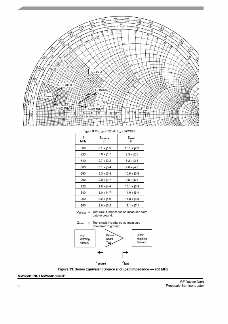
f
MHz
Zsource
Ω
Zload
Ω
800
820
840
31 + j19
27 + j22
28 + j17
101 + j23
83 + j25
82 + j33
VDD = 28 Vdc IDQ = 125 mA Pout = 10 W PEP
860
880
900
31 + j34
29 + j37
33 + j38
98 + j48
106 + j56
95 + j55
920
940
960
28 + j44
32 + j49
30 + j47
101 + j59
110 + j64
118 + j66
980 36 + j52 121 + j71
Figure 13 Series Equivalent Source and Load Impedance mdash 900 MHz
Zsource = Test circuit impedance as measured fromgate to ground
Zload = Test circuit impedance as measured
from drain to ground
Zsource
Zload
Input
Matching
Network
Device
Under
Test
Output
Matching
Network
f = 800 MHz
f = 980 MHz
Zo = 25 Ω
f = 800 MHz
f = 980 MHz
Zload
Zsource
8122019 MW6S010N
httpslidepdfcomreaderfullmw6s010n 920
MW6S010NR1 MW6S010GNR1
9RF Device DataFreescale Semiconductor
Figure 14 MW6S010NR1(GNR1) Test Circuit Schematic mdash 450 MHz
C5
C2
+
RF
OUTPUT
C6
VBIAS
VSUPPLY
RF
INPUT Z1
C9
Z5
R6
DUT
B2
C4
Z6
L1
C12 C11C10
Z5 0475Prime x 0330Prime Microstrip
Z6 0475Prime x 0325Prime Microstrip
Z8 1250Prime x 0080Prime Microstrip
PCB Rogers ULTRALAM 2000 0030Prime εr = 255
Z1 0540Prime x 0080Prime Microstrip
Z2 0365Prime x 0080Prime Microstrip
Z3 0225Prime x 0080Prime Microstrip
Z4 Z7 0440Prime x 0080Prime Microstrip
C7
Z2
C8
Z3 Z4
C3
C1
+
R2R5
R1T1
R3
R4
T2
Z8Z7
B1
C13 C14 C15
+
Table 7 MW6S010NR1(GNR1) Test Circuit Component Designations and Values mdash 450 MHz
Part Description Part Number Manufacturer
B1 B2 Ferrite Bead 2743019447 Fair -Rite
C1 1 microF 35 V Tantalum Capacitor T491C105K050AT Kemet
C2 C15 22 microF 35 V Tantalum Capacitors T491X226K035AT Kemet
VDD = 28 Vdc Pout = 75 W (Avg) IDQ = 150 mA2minusCarrier WminusCDMA 10 MHz Carrier Spacing384 MHz Channel Bandwidth PAR = 85 dB 001 Probability (CCDF)
ALT1
ACPR
Gps
Figure 19 Single-Carrier N-CDMA ACPR ALT1
and ALT2 versus Output Power
minus80
Pout OUTPUT POWER (WATTS) AVG
minus10
minus20
minus30
minus40
minus70
01 1 10
minus50
ACPR
VDD = 28 Vdc IDQ = 150 mA
f = 450 MHz NminusCDMA ISminus95 Pilot
Sync Paging Traffic Codes 8
Through 13
A L T 1 amp A L T 2
C H A N N E L P O W E R
d B c
A C P R
A D J A C E
N T C H A N N E L P O W E R R A T I O ( d B c )
minus60
ALT2
ALT1
8122019 MW6S010N
httpslidepdfcomreaderfullmw6s010n 1220 12
RF Device DataFreescale Semiconductor
MW6S010NR1 MW6S010GNR1
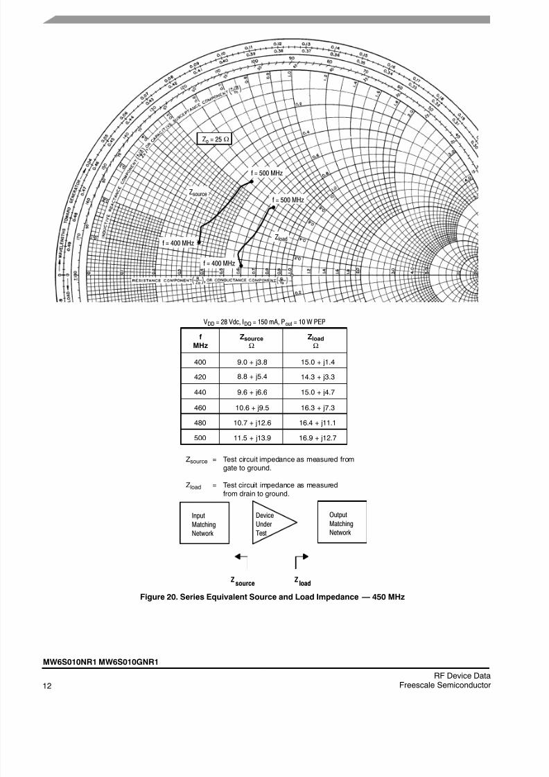
f
MHz
Zsource
Ω
Zload
Ω
400
420
440
90 + j38
96 + j66
88 + j54
150 + j14
143 + j33
150 + j47
VDD = 28 Vdc IDQ = 150 mA Pout = 10 W PEP
460
480
500
106 + j95
115 + j139
107 + j126
163 + j73
164 + j111
169 + j127
Figure 20 Series Equivalent Source and Load Impedance mdash 450 MHz
Zsource = Test circuit impedance as measured fromgate to ground
Zload = Test circuit impedance as measuredfrom drain to ground
Zsource
Zload
Input
Matching
Network
Device
Under
Test
Output
Matching
Network
f = 400 MHz
Zo = 25 Ω
Zload
Zsource
f = 500 MHz
f = 400 MHz
f = 500 MHz
8122019 MW6S010N
httpslidepdfcomreaderfullmw6s010n 1320
MW6S010NR1 MW6S010GNR1
13RF Device DataFreescale Semiconductor
PACKAGE DIMENSIONS
8122019 MW6S010N
httpslidepdfcomreaderfullmw6s010n 1420 14
RF Device DataFreescale Semiconductor
MW6S010NR1 MW6S010GNR1
8122019 MW6S010N
httpslidepdfcomreaderfullmw6s010n 1520
MW6S010NR1 MW6S010GNR1
15RF Device DataFreescale Semiconductor
8122019 MW6S010N
httpslidepdfcomreaderfullmw6s010n 1620 16
RF Device DataFreescale Semiconductor
MW6S010NR1 MW6S010GNR1
8122019 MW6S010N
httpslidepdfcomreaderfullmw6s010n 1720
MW6S010NR1 MW6S010GNR1
17RF Device DataFreescale Semiconductor
8122019 MW6S010N
httpslidepdfcomreaderfullmw6s010n 1820 18
RF Device DataFreescale Semiconductor
MW6S010NR1 MW6S010GNR1
8122019 MW6S010N
httpslidepdfcomreaderfullmw6s010n 1920
MW6S010NR1 MW6S010GNR1
19RF Device DataFreescale Semiconductor
PRODUCT DOCUMENTATION TOOLS AND SOFTWARE
Refer to the following documents to aid your design process
Application Notes
bull AN1907 Solder Reflow Attach Method for High Power RF Devices in Plastic Packages
bull AN1949 Mounting Method for the MHVIC910HR2 (PFP- 16) and Similar Surface Mount Packages
bull AN1955 Thermal Measurement Methodology of RF Power Amplifiers
bull AN3789 Clamping of High Power RF Transistors and RFICs in Over- Molded Plastic Packages
Engineering Bulletinsbull EB212 Using Data Sheet Impedances for RF LDMOS Devices
Software
bull Electromigration MTTF Calculator
bull RF High Power Model
For Software and Tools do a Part Number search at httpwwwfreescalecom and select the ldquoPart Numberrdquo link Go to the
Software amp Tools tab on the partrsquos Product Summary page to download the respective tool
REVISION HISTORY
The following table summarizes revisions to this document
Revision Date Description
4 Dec 2008 bull Changed Storage Temperature Range in Max Ratings table from -65 to +175 to -65 to +150 for
standardization across products p 1
bull Removed Total Device Dissipation from Max Ratings table as data was redundant (information already
provided in Thermal Characteristics table) p 1
bull Added Case Operating Temperature limit to the Maximum Ratings table and set limit to 150degC p 1
bull Operating Junction Temperature increased from 200degC to 225degC in Maximum Ratings table related
ldquoContinuous use at maximum temperature will affect MTTFrdquo footnote added and changed 200degC to 225degC in
Capable Plastic Package bullet p 1
bull Corrected VDS to VDD in the RF test condition voltage callout for VGS(Q) and added ldquoMeasured in Functional
Testrdquo On Characteristics table p 2
bull Corrected Ciss test condition to indicate AC stimulus on the VGS connection versus the VDS connection
Dynamic Characteristics table p 2bull Updated Part Numbers in Tables 6 7 Component Designations and Values to RoHS compliant part
numbers p 3 9
bull Removed lower voltage tests from Fig 10 Power Gain versus Output Power due to fixed tuned fixture
limitations p 6
bull Replaced Fig 12 MTTF versus Junction Temperature with updated graph Removed Amps2 and listed
operating characteristics and location of MTTF calculator for device p 7
bull Replaced Case Outline 1265-08 with 1265-09 Issue K p 1 13-15 Corrected cross hatch pattern in
bottom view and changed its dimensions (D2 and E3) to minimum value on source contact (D2 changed
from Min-Max 290-320 to 290 Min E3 changed from Min-Max 150-180 to 150 Min) Added JEDEC
Standard Package Number
bull Replaced Case Outline 1265A-02 with 1265A-03 Issue C p 1 16-18 Corrected cross hatch pattern and
its dimensions (D2 and E2) on source contact (D2 changed from Min-Max 290-320 to 290 Min E3
changed from Min-Max 150-180 to 150 Min) Added pin numbers Corrected mm dimension L for
gull-wing foot from 490-506 Min-Max to 046-061 Min-Max Added JEDEC Standard Package Number
bull Added Product Documentation and Revision History p 19
5 June 2009 bull Modified data sheet to reflect MSL rating change from 1 to 3 as a result of the standardization of packing
process as described in Product and Process Change Notification number PCN13516 p 2
bull Added AN3789 Clamping of High Power RF Transistors and RFICs in Over- Molded Plastic Packages to
Product Documentation Application Notes p 19
bull Added Electromigration MTTF Calculator and RF High Power Model availability to Product Software p 19
8122019 MW6S010N
httpslidepdfcomreaderfullmw6s010n 2020
MW6S010NR1 MW6S010GNR1
Information in this document is provided solely to enable system and software
implementers to use Freescale Semiconductor products There are no express or
implied copyright licenses granted hereunder to design or fabricate any integrated
circuits or integrated circuits based on the information in this document
Freescale Semiconductor reserves the right to make changes without further notice to
any products herein Freescale Semiconductor makes no warranty representation or
guarantee regarding the suitability of its products for any particular purpose nor does
Freescale Semiconductor assume any liability arising out of the application or use of
any product or circuit and specifically disclaims any and all liability including without
limitation consequential or incidental damages ldquoTypicalrdquo parameters that may be
provided in Freescale Semiconductor data sheets andor specifications can and dovary in different applications and actual performance may vary over time All operating
parameters including ldquoTypicalsrdquo must be validated for each customer application by
customerrsquos technical experts Freescale Semiconductor does not convey any license
under its patent rights nor the rights of others Freescale Semiconductor products are
not designed intended or authorized for use as components in systems intended for
surgical implant into the body or other applications intended to support or sustain life
or for any other application in which the failure of the Freescale Semiconductor product
could create a situation where personal injury or death may occur Should Buyer
purchase or use Freescale Semiconductor products for any such unintended or
unauthorized application Buyer shall indemnify and hold Freescale Semiconductor
and its officers employees subsidiaries affiliates and distributors harmless against all
claims costs damages and expenses and reasonable attorney fees arising out of
directly or indirectly any claim of personal injury or death associated with such
unintended or unauthorized use even if such claim alleges that Freescale
Semiconductor was negligent regarding the design or manufacture of the part
Freescale and the Freescale logo are trademarks of Freescale Semiconductor Inc
All other product or service names are the property of their respective owners
copy Freescale Semiconductor Inc 2005-2006 2008- 2009 All rights reserved
How to Reach Us
Home Pagewwwfreescalecom
Web Supporthttpwwwfreescalecomsupport
USAEurope or Locations Not ListedFreescale Semiconductor IncTechnical Information Center EL5162100 East Elliot Road
Tempe Arizona 852841-800-521-6274 or +1-480-768-2130wwwfreescalecomsupport
Europe Middle East and AfricaFreescale Halbleiter Deutschland GmbHTechnical Information CenterSchatzbogen 781829 Muenchen Germany+44 1296 380 456 (English)+46 8 52200080 (English)+49 89 92103 559 (German)+33 1 69 35 48 48 (French)wwwfreescalecomsupport
JapanFreescale Semiconductor Japan LtdHeadquarters ARCO Tower 15F1-8-1 Shimo-Meguro Meguro-kuTokyo 153-0064Japan0120 191014 or +81 3 5437 9125supportjapanfreescalecom
AsiaPacificFreescale Semiconductor China LtdExchange Building 23FNo 118 Jianguo RoadChaoyang DistrictBeijing 100022China+86 10 5879 8000supportasiafreescalecom
For Literature Requests OnlyFreescale Semiconductor Literature Distribution Center1-800-441-2447 or +1-303-675-2140Fax +1- 303-675- 2150LDCForFreescaleSemiconductorhibbertgroupcom
8122019 MW6S010N
httpslidepdfcomreaderfullmw6s010n 720
MW6S010NR1 MW6S010GNR1
7RF Device DataFreescale Semiconductor
TYPICAL CHARACTERISTICS
Figure 12 MTTF Factor versus Junction Temperature
250
108
90
TJ JUNCTION TEMPERATURE (degC)
This above graph displays calculated MTTF in hours when the device
is operated at VDD = 28 Vdc Pout = 10 W PEP and ηD = 32
MTTF calculator available at httpwwwfreescalecomrf Select
Software amp ToolsDevelopment ToolsCalculators to access MTTF
calculators by product
106
105
104
110 130 150 170 190
M T T F
( H O U R S )
210 230
107
8122019 MW6S010N
httpslidepdfcomreaderfullmw6s010n 820 8
RF Device DataFreescale Semiconductor
MW6S010NR1 MW6S010GNR1
f
MHz
Zsource
Ω
Zload
Ω
800
820
840
31 + j19
27 + j22
28 + j17
101 + j23
83 + j25
82 + j33
VDD = 28 Vdc IDQ = 125 mA Pout = 10 W PEP
860
880
900
31 + j34
29 + j37
33 + j38
98 + j48
106 + j56
95 + j55
920
940
960
28 + j44
32 + j49
30 + j47
101 + j59
110 + j64
118 + j66
980 36 + j52 121 + j71
Figure 13 Series Equivalent Source and Load Impedance mdash 900 MHz
Zsource = Test circuit impedance as measured fromgate to ground
Zload = Test circuit impedance as measured
from drain to ground
Zsource
Zload
Input
Matching
Network
Device
Under
Test
Output
Matching
Network
f = 800 MHz
f = 980 MHz
Zo = 25 Ω
f = 800 MHz
f = 980 MHz
Zload
Zsource
8122019 MW6S010N
httpslidepdfcomreaderfullmw6s010n 920
MW6S010NR1 MW6S010GNR1
9RF Device DataFreescale Semiconductor
Figure 14 MW6S010NR1(GNR1) Test Circuit Schematic mdash 450 MHz
C5
C2
+
RF
OUTPUT
C6
VBIAS
VSUPPLY
RF
INPUT Z1
C9
Z5
R6
DUT
B2
C4
Z6
L1
C12 C11C10
Z5 0475Prime x 0330Prime Microstrip
Z6 0475Prime x 0325Prime Microstrip
Z8 1250Prime x 0080Prime Microstrip
PCB Rogers ULTRALAM 2000 0030Prime εr = 255
Z1 0540Prime x 0080Prime Microstrip
Z2 0365Prime x 0080Prime Microstrip
Z3 0225Prime x 0080Prime Microstrip
Z4 Z7 0440Prime x 0080Prime Microstrip
C7
Z2
C8
Z3 Z4
C3
C1
+
R2R5
R1T1
R3
R4
T2
Z8Z7
B1
C13 C14 C15
+
Table 7 MW6S010NR1(GNR1) Test Circuit Component Designations and Values mdash 450 MHz
Part Description Part Number Manufacturer
B1 B2 Ferrite Bead 2743019447 Fair -Rite
C1 1 microF 35 V Tantalum Capacitor T491C105K050AT Kemet
C2 C15 22 microF 35 V Tantalum Capacitors T491X226K035AT Kemet
VDD = 28 Vdc Pout = 75 W (Avg) IDQ = 150 mA2minusCarrier WminusCDMA 10 MHz Carrier Spacing384 MHz Channel Bandwidth PAR = 85 dB 001 Probability (CCDF)
ALT1
ACPR
Gps
Figure 19 Single-Carrier N-CDMA ACPR ALT1
and ALT2 versus Output Power
minus80
Pout OUTPUT POWER (WATTS) AVG
minus10
minus20
minus30
minus40
minus70
01 1 10
minus50
ACPR
VDD = 28 Vdc IDQ = 150 mA
f = 450 MHz NminusCDMA ISminus95 Pilot
Sync Paging Traffic Codes 8
Through 13
A L T 1 amp A L T 2
C H A N N E L P O W E R
d B c
A C P R
A D J A C E
N T C H A N N E L P O W E R R A T I O ( d B c )
minus60
ALT2
ALT1
8122019 MW6S010N
httpslidepdfcomreaderfullmw6s010n 1220 12
RF Device DataFreescale Semiconductor
MW6S010NR1 MW6S010GNR1
f
MHz
Zsource
Ω
Zload
Ω
400
420
440
90 + j38
96 + j66
88 + j54
150 + j14
143 + j33
150 + j47
VDD = 28 Vdc IDQ = 150 mA Pout = 10 W PEP
460
480
500
106 + j95
115 + j139
107 + j126
163 + j73
164 + j111
169 + j127
Figure 20 Series Equivalent Source and Load Impedance mdash 450 MHz
Zsource = Test circuit impedance as measured fromgate to ground
Zload = Test circuit impedance as measuredfrom drain to ground
Zsource
Zload
Input
Matching
Network
Device
Under
Test
Output
Matching
Network
f = 400 MHz
Zo = 25 Ω
Zload
Zsource
f = 500 MHz
f = 400 MHz
f = 500 MHz
8122019 MW6S010N
httpslidepdfcomreaderfullmw6s010n 1320
MW6S010NR1 MW6S010GNR1
13RF Device DataFreescale Semiconductor
PACKAGE DIMENSIONS
8122019 MW6S010N
httpslidepdfcomreaderfullmw6s010n 1420 14
RF Device DataFreescale Semiconductor
MW6S010NR1 MW6S010GNR1
8122019 MW6S010N
httpslidepdfcomreaderfullmw6s010n 1520
MW6S010NR1 MW6S010GNR1
15RF Device DataFreescale Semiconductor
8122019 MW6S010N
httpslidepdfcomreaderfullmw6s010n 1620 16
RF Device DataFreescale Semiconductor
MW6S010NR1 MW6S010GNR1
8122019 MW6S010N
httpslidepdfcomreaderfullmw6s010n 1720
MW6S010NR1 MW6S010GNR1
17RF Device DataFreescale Semiconductor
8122019 MW6S010N
httpslidepdfcomreaderfullmw6s010n 1820 18
RF Device DataFreescale Semiconductor
MW6S010NR1 MW6S010GNR1
8122019 MW6S010N
httpslidepdfcomreaderfullmw6s010n 1920
MW6S010NR1 MW6S010GNR1
19RF Device DataFreescale Semiconductor
PRODUCT DOCUMENTATION TOOLS AND SOFTWARE
Refer to the following documents to aid your design process
Application Notes
bull AN1907 Solder Reflow Attach Method for High Power RF Devices in Plastic Packages
bull AN1949 Mounting Method for the MHVIC910HR2 (PFP- 16) and Similar Surface Mount Packages
bull AN1955 Thermal Measurement Methodology of RF Power Amplifiers
bull AN3789 Clamping of High Power RF Transistors and RFICs in Over- Molded Plastic Packages
Engineering Bulletinsbull EB212 Using Data Sheet Impedances for RF LDMOS Devices
Software
bull Electromigration MTTF Calculator
bull RF High Power Model
For Software and Tools do a Part Number search at httpwwwfreescalecom and select the ldquoPart Numberrdquo link Go to the
Software amp Tools tab on the partrsquos Product Summary page to download the respective tool
REVISION HISTORY
The following table summarizes revisions to this document
Revision Date Description
4 Dec 2008 bull Changed Storage Temperature Range in Max Ratings table from -65 to +175 to -65 to +150 for
standardization across products p 1
bull Removed Total Device Dissipation from Max Ratings table as data was redundant (information already
provided in Thermal Characteristics table) p 1
bull Added Case Operating Temperature limit to the Maximum Ratings table and set limit to 150degC p 1
bull Operating Junction Temperature increased from 200degC to 225degC in Maximum Ratings table related
ldquoContinuous use at maximum temperature will affect MTTFrdquo footnote added and changed 200degC to 225degC in
Capable Plastic Package bullet p 1
bull Corrected VDS to VDD in the RF test condition voltage callout for VGS(Q) and added ldquoMeasured in Functional
Testrdquo On Characteristics table p 2
bull Corrected Ciss test condition to indicate AC stimulus on the VGS connection versus the VDS connection
Dynamic Characteristics table p 2bull Updated Part Numbers in Tables 6 7 Component Designations and Values to RoHS compliant part
numbers p 3 9
bull Removed lower voltage tests from Fig 10 Power Gain versus Output Power due to fixed tuned fixture
limitations p 6
bull Replaced Fig 12 MTTF versus Junction Temperature with updated graph Removed Amps2 and listed
operating characteristics and location of MTTF calculator for device p 7
bull Replaced Case Outline 1265-08 with 1265-09 Issue K p 1 13-15 Corrected cross hatch pattern in
bottom view and changed its dimensions (D2 and E3) to minimum value on source contact (D2 changed
from Min-Max 290-320 to 290 Min E3 changed from Min-Max 150-180 to 150 Min) Added JEDEC
Standard Package Number
bull Replaced Case Outline 1265A-02 with 1265A-03 Issue C p 1 16-18 Corrected cross hatch pattern and
its dimensions (D2 and E2) on source contact (D2 changed from Min-Max 290-320 to 290 Min E3
changed from Min-Max 150-180 to 150 Min) Added pin numbers Corrected mm dimension L for
gull-wing foot from 490-506 Min-Max to 046-061 Min-Max Added JEDEC Standard Package Number
bull Added Product Documentation and Revision History p 19
5 June 2009 bull Modified data sheet to reflect MSL rating change from 1 to 3 as a result of the standardization of packing
process as described in Product and Process Change Notification number PCN13516 p 2
bull Added AN3789 Clamping of High Power RF Transistors and RFICs in Over- Molded Plastic Packages to
Product Documentation Application Notes p 19
bull Added Electromigration MTTF Calculator and RF High Power Model availability to Product Software p 19
8122019 MW6S010N
httpslidepdfcomreaderfullmw6s010n 2020
MW6S010NR1 MW6S010GNR1
Information in this document is provided solely to enable system and software
implementers to use Freescale Semiconductor products There are no express or
implied copyright licenses granted hereunder to design or fabricate any integrated
circuits or integrated circuits based on the information in this document
Freescale Semiconductor reserves the right to make changes without further notice to
any products herein Freescale Semiconductor makes no warranty representation or
guarantee regarding the suitability of its products for any particular purpose nor does
Freescale Semiconductor assume any liability arising out of the application or use of
any product or circuit and specifically disclaims any and all liability including without
limitation consequential or incidental damages ldquoTypicalrdquo parameters that may be
provided in Freescale Semiconductor data sheets andor specifications can and dovary in different applications and actual performance may vary over time All operating
parameters including ldquoTypicalsrdquo must be validated for each customer application by
customerrsquos technical experts Freescale Semiconductor does not convey any license
under its patent rights nor the rights of others Freescale Semiconductor products are
not designed intended or authorized for use as components in systems intended for
surgical implant into the body or other applications intended to support or sustain life
or for any other application in which the failure of the Freescale Semiconductor product
could create a situation where personal injury or death may occur Should Buyer
purchase or use Freescale Semiconductor products for any such unintended or
unauthorized application Buyer shall indemnify and hold Freescale Semiconductor
and its officers employees subsidiaries affiliates and distributors harmless against all
claims costs damages and expenses and reasonable attorney fees arising out of
directly or indirectly any claim of personal injury or death associated with such
unintended or unauthorized use even if such claim alleges that Freescale
Semiconductor was negligent regarding the design or manufacture of the part
Freescale and the Freescale logo are trademarks of Freescale Semiconductor Inc
All other product or service names are the property of their respective owners
copy Freescale Semiconductor Inc 2005-2006 2008- 2009 All rights reserved
How to Reach Us
Home Pagewwwfreescalecom
Web Supporthttpwwwfreescalecomsupport
USAEurope or Locations Not ListedFreescale Semiconductor IncTechnical Information Center EL5162100 East Elliot Road
Tempe Arizona 852841-800-521-6274 or +1-480-768-2130wwwfreescalecomsupport
Europe Middle East and AfricaFreescale Halbleiter Deutschland GmbHTechnical Information CenterSchatzbogen 781829 Muenchen Germany+44 1296 380 456 (English)+46 8 52200080 (English)+49 89 92103 559 (German)+33 1 69 35 48 48 (French)wwwfreescalecomsupport
JapanFreescale Semiconductor Japan LtdHeadquarters ARCO Tower 15F1-8-1 Shimo-Meguro Meguro-kuTokyo 153-0064Japan0120 191014 or +81 3 5437 9125supportjapanfreescalecom
AsiaPacificFreescale Semiconductor China LtdExchange Building 23FNo 118 Jianguo RoadChaoyang DistrictBeijing 100022China+86 10 5879 8000supportasiafreescalecom
For Literature Requests OnlyFreescale Semiconductor Literature Distribution Center1-800-441-2447 or +1-303-675-2140Fax +1- 303-675- 2150LDCForFreescaleSemiconductorhibbertgroupcom
8122019 MW6S010N
httpslidepdfcomreaderfullmw6s010n 1020 10
RF Device DataFreescale Semiconductor
MW6S010NR1 MW6S010GNR1
Figure 15 MW6S010NR1(GNR1) Test Circuit Component Layout mdash 450 MHz
VDD = 28 Vdc Pout = 75 W (Avg) IDQ = 150 mA2minusCarrier WminusCDMA 10 MHz Carrier Spacing384 MHz Channel Bandwidth PAR = 85 dB 001 Probability (CCDF)
ALT1
ACPR
Gps
Figure 19 Single-Carrier N-CDMA ACPR ALT1
and ALT2 versus Output Power
minus80
Pout OUTPUT POWER (WATTS) AVG
minus10
minus20
minus30
minus40
minus70
01 1 10
minus50
ACPR
VDD = 28 Vdc IDQ = 150 mA
f = 450 MHz NminusCDMA ISminus95 Pilot
Sync Paging Traffic Codes 8
Through 13
A L T 1 amp A L T 2
C H A N N E L P O W E R
d B c
A C P R
A D J A C E
N T C H A N N E L P O W E R R A T I O ( d B c )
minus60
ALT2
ALT1
8122019 MW6S010N
httpslidepdfcomreaderfullmw6s010n 1220 12
RF Device DataFreescale Semiconductor
MW6S010NR1 MW6S010GNR1
f
MHz
Zsource
Ω
Zload
Ω
400
420
440
90 + j38
96 + j66
88 + j54
150 + j14
143 + j33
150 + j47
VDD = 28 Vdc IDQ = 150 mA Pout = 10 W PEP
460
480
500
106 + j95
115 + j139
107 + j126
163 + j73
164 + j111
169 + j127
Figure 20 Series Equivalent Source and Load Impedance mdash 450 MHz
Zsource = Test circuit impedance as measured fromgate to ground
Zload = Test circuit impedance as measuredfrom drain to ground
Zsource
Zload
Input
Matching
Network
Device
Under
Test
Output
Matching
Network
f = 400 MHz
Zo = 25 Ω
Zload
Zsource
f = 500 MHz
f = 400 MHz
f = 500 MHz
8122019 MW6S010N
httpslidepdfcomreaderfullmw6s010n 1320
MW6S010NR1 MW6S010GNR1
13RF Device DataFreescale Semiconductor
PACKAGE DIMENSIONS
8122019 MW6S010N
httpslidepdfcomreaderfullmw6s010n 1420 14
RF Device DataFreescale Semiconductor
MW6S010NR1 MW6S010GNR1
8122019 MW6S010N
httpslidepdfcomreaderfullmw6s010n 1520
MW6S010NR1 MW6S010GNR1
15RF Device DataFreescale Semiconductor
8122019 MW6S010N
httpslidepdfcomreaderfullmw6s010n 1620 16
RF Device DataFreescale Semiconductor
MW6S010NR1 MW6S010GNR1
8122019 MW6S010N
httpslidepdfcomreaderfullmw6s010n 1720
MW6S010NR1 MW6S010GNR1
17RF Device DataFreescale Semiconductor
8122019 MW6S010N
httpslidepdfcomreaderfullmw6s010n 1820 18
RF Device DataFreescale Semiconductor
MW6S010NR1 MW6S010GNR1
8122019 MW6S010N
httpslidepdfcomreaderfullmw6s010n 1920
MW6S010NR1 MW6S010GNR1
19RF Device DataFreescale Semiconductor
PRODUCT DOCUMENTATION TOOLS AND SOFTWARE
Refer to the following documents to aid your design process
Application Notes
bull AN1907 Solder Reflow Attach Method for High Power RF Devices in Plastic Packages
bull AN1949 Mounting Method for the MHVIC910HR2 (PFP- 16) and Similar Surface Mount Packages
bull AN1955 Thermal Measurement Methodology of RF Power Amplifiers
bull AN3789 Clamping of High Power RF Transistors and RFICs in Over- Molded Plastic Packages
Engineering Bulletinsbull EB212 Using Data Sheet Impedances for RF LDMOS Devices
Software
bull Electromigration MTTF Calculator
bull RF High Power Model
For Software and Tools do a Part Number search at httpwwwfreescalecom and select the ldquoPart Numberrdquo link Go to the
Software amp Tools tab on the partrsquos Product Summary page to download the respective tool
REVISION HISTORY
The following table summarizes revisions to this document
Revision Date Description
4 Dec 2008 bull Changed Storage Temperature Range in Max Ratings table from -65 to +175 to -65 to +150 for
standardization across products p 1
bull Removed Total Device Dissipation from Max Ratings table as data was redundant (information already
provided in Thermal Characteristics table) p 1
bull Added Case Operating Temperature limit to the Maximum Ratings table and set limit to 150degC p 1
bull Operating Junction Temperature increased from 200degC to 225degC in Maximum Ratings table related
ldquoContinuous use at maximum temperature will affect MTTFrdquo footnote added and changed 200degC to 225degC in
Capable Plastic Package bullet p 1
bull Corrected VDS to VDD in the RF test condition voltage callout for VGS(Q) and added ldquoMeasured in Functional
Testrdquo On Characteristics table p 2
bull Corrected Ciss test condition to indicate AC stimulus on the VGS connection versus the VDS connection
Dynamic Characteristics table p 2bull Updated Part Numbers in Tables 6 7 Component Designations and Values to RoHS compliant part
numbers p 3 9
bull Removed lower voltage tests from Fig 10 Power Gain versus Output Power due to fixed tuned fixture
limitations p 6
bull Replaced Fig 12 MTTF versus Junction Temperature with updated graph Removed Amps2 and listed
operating characteristics and location of MTTF calculator for device p 7
bull Replaced Case Outline 1265-08 with 1265-09 Issue K p 1 13-15 Corrected cross hatch pattern in
bottom view and changed its dimensions (D2 and E3) to minimum value on source contact (D2 changed
from Min-Max 290-320 to 290 Min E3 changed from Min-Max 150-180 to 150 Min) Added JEDEC
Standard Package Number
bull Replaced Case Outline 1265A-02 with 1265A-03 Issue C p 1 16-18 Corrected cross hatch pattern and
its dimensions (D2 and E2) on source contact (D2 changed from Min-Max 290-320 to 290 Min E3
changed from Min-Max 150-180 to 150 Min) Added pin numbers Corrected mm dimension L for
gull-wing foot from 490-506 Min-Max to 046-061 Min-Max Added JEDEC Standard Package Number
bull Added Product Documentation and Revision History p 19
5 June 2009 bull Modified data sheet to reflect MSL rating change from 1 to 3 as a result of the standardization of packing
process as described in Product and Process Change Notification number PCN13516 p 2
bull Added AN3789 Clamping of High Power RF Transistors and RFICs in Over- Molded Plastic Packages to
Product Documentation Application Notes p 19
bull Added Electromigration MTTF Calculator and RF High Power Model availability to Product Software p 19
8122019 MW6S010N
httpslidepdfcomreaderfullmw6s010n 2020
MW6S010NR1 MW6S010GNR1
Information in this document is provided solely to enable system and software
implementers to use Freescale Semiconductor products There are no express or
implied copyright licenses granted hereunder to design or fabricate any integrated
circuits or integrated circuits based on the information in this document
Freescale Semiconductor reserves the right to make changes without further notice to
any products herein Freescale Semiconductor makes no warranty representation or
guarantee regarding the suitability of its products for any particular purpose nor does
Freescale Semiconductor assume any liability arising out of the application or use of
any product or circuit and specifically disclaims any and all liability including without
limitation consequential or incidental damages ldquoTypicalrdquo parameters that may be
provided in Freescale Semiconductor data sheets andor specifications can and dovary in different applications and actual performance may vary over time All operating
parameters including ldquoTypicalsrdquo must be validated for each customer application by
customerrsquos technical experts Freescale Semiconductor does not convey any license
under its patent rights nor the rights of others Freescale Semiconductor products are
not designed intended or authorized for use as components in systems intended for
surgical implant into the body or other applications intended to support or sustain life
or for any other application in which the failure of the Freescale Semiconductor product
could create a situation where personal injury or death may occur Should Buyer
purchase or use Freescale Semiconductor products for any such unintended or
unauthorized application Buyer shall indemnify and hold Freescale Semiconductor
and its officers employees subsidiaries affiliates and distributors harmless against all
claims costs damages and expenses and reasonable attorney fees arising out of
directly or indirectly any claim of personal injury or death associated with such
unintended or unauthorized use even if such claim alleges that Freescale
Semiconductor was negligent regarding the design or manufacture of the part
Freescale and the Freescale logo are trademarks of Freescale Semiconductor Inc
All other product or service names are the property of their respective owners
copy Freescale Semiconductor Inc 2005-2006 2008- 2009 All rights reserved
How to Reach Us
Home Pagewwwfreescalecom
Web Supporthttpwwwfreescalecomsupport
USAEurope or Locations Not ListedFreescale Semiconductor IncTechnical Information Center EL5162100 East Elliot Road
Tempe Arizona 852841-800-521-6274 or +1-480-768-2130wwwfreescalecomsupport
Europe Middle East and AfricaFreescale Halbleiter Deutschland GmbHTechnical Information CenterSchatzbogen 781829 Muenchen Germany+44 1296 380 456 (English)+46 8 52200080 (English)+49 89 92103 559 (German)+33 1 69 35 48 48 (French)wwwfreescalecomsupport
JapanFreescale Semiconductor Japan LtdHeadquarters ARCO Tower 15F1-8-1 Shimo-Meguro Meguro-kuTokyo 153-0064Japan0120 191014 or +81 3 5437 9125supportjapanfreescalecom
AsiaPacificFreescale Semiconductor China LtdExchange Building 23FNo 118 Jianguo RoadChaoyang DistrictBeijing 100022China+86 10 5879 8000supportasiafreescalecom
For Literature Requests OnlyFreescale Semiconductor Literature Distribution Center1-800-441-2447 or +1-303-675-2140Fax +1- 303-675- 2150LDCForFreescaleSemiconductorhibbertgroupcom
8122019 MW6S010N
httpslidepdfcomreaderfullmw6s010n 2020
MW6S010NR1 MW6S010GNR1
Information in this document is provided solely to enable system and software
implementers to use Freescale Semiconductor products There are no express or
implied copyright licenses granted hereunder to design or fabricate any integrated
circuits or integrated circuits based on the information in this document
Freescale Semiconductor reserves the right to make changes without further notice to
any products herein Freescale Semiconductor makes no warranty representation or
guarantee regarding the suitability of its products for any particular purpose nor does
Freescale Semiconductor assume any liability arising out of the application or use of
any product or circuit and specifically disclaims any and all liability including without
limitation consequential or incidental damages ldquoTypicalrdquo parameters that may be
provided in Freescale Semiconductor data sheets andor specifications can and dovary in different applications and actual performance may vary over time All operating
parameters including ldquoTypicalsrdquo must be validated for each customer application by
customerrsquos technical experts Freescale Semiconductor does not convey any license
under its patent rights nor the rights of others Freescale Semiconductor products are
not designed intended or authorized for use as components in systems intended for
surgical implant into the body or other applications intended to support or sustain life
or for any other application in which the failure of the Freescale Semiconductor product
could create a situation where personal injury or death may occur Should Buyer
purchase or use Freescale Semiconductor products for any such unintended or
unauthorized application Buyer shall indemnify and hold Freescale Semiconductor
and its officers employees subsidiaries affiliates and distributors harmless against all
claims costs damages and expenses and reasonable attorney fees arising out of
directly or indirectly any claim of personal injury or death associated with such
unintended or unauthorized use even if such claim alleges that Freescale
Semiconductor was negligent regarding the design or manufacture of the part
Freescale and the Freescale logo are trademarks of Freescale Semiconductor Inc
All other product or service names are the property of their respective owners
copy Freescale Semiconductor Inc 2005-2006 2008- 2009 All rights reserved
How to Reach Us
Home Pagewwwfreescalecom
Web Supporthttpwwwfreescalecomsupport
USAEurope or Locations Not ListedFreescale Semiconductor IncTechnical Information Center EL5162100 East Elliot Road
Tempe Arizona 852841-800-521-6274 or +1-480-768-2130wwwfreescalecomsupport
Europe Middle East and AfricaFreescale Halbleiter Deutschland GmbHTechnical Information CenterSchatzbogen 781829 Muenchen Germany+44 1296 380 456 (English)+46 8 52200080 (English)+49 89 92103 559 (German)+33 1 69 35 48 48 (French)wwwfreescalecomsupport
JapanFreescale Semiconductor Japan LtdHeadquarters ARCO Tower 15F1-8-1 Shimo-Meguro Meguro-kuTokyo 153-0064Japan0120 191014 or +81 3 5437 9125supportjapanfreescalecom
AsiaPacificFreescale Semiconductor China LtdExchange Building 23FNo 118 Jianguo RoadChaoyang DistrictBeijing 100022China+86 10 5879 8000supportasiafreescalecom
For Literature Requests OnlyFreescale Semiconductor Literature Distribution Center1-800-441-2447 or +1-303-675-2140Fax +1- 303-675- 2150LDCForFreescaleSemiconductorhibbertgroupcom