82
1 P/N:PM1494 REV. 1.6, OCT. 30, 2013 MX29GL640E T/B MX29GL640E H/L MX29GL640E T/B, MX29GL640E H/L DATASHEET

1P/N:PM1494 REV. 1.6, OCT. 30, 2013
MX29GL640E T/BMX29GL640E H/L
MX29GL640E T/B, MX29GL640E H/L
DATASHEET

2P/N:PM1494 REV. 1.6, OCT. 30, 2013
MX29GL640E T/BMX29GL640E H/L
Contents
FEATURES .............................................................................................................................................................5PIN CONFIGURATION for MX29GL640E T/B .......................................................................................................6PIN CONFIGURATION for MX29GL640E H/L .......................................................................................................7PIN DESCRIPTION .................................................................................................................................................8BLOCK DIAGRAM ..................................................................................................................................................9BLOCK DIAGRAM DESCRIPTION ......................................................................................................................10BLOCK STRUCTURE ........................................................................................................................................... 11
Table 1-1. MX29GL640ET SECTOR ARCHITECTURE ............................................................................. 11Table 1-2. MX29GL640EB SECTOR ARCHITECTURE .............................................................................15Table 1-3. MX29GL640E H/L SECTOR ARCHITECTURE .........................................................................19
FUNCTIONAL OPERATION DESCRIPTION .......................................................................................................24READ OPERATION ....................................................................................................................................24PAGE READ ................................................................................................................................................24WRITE OPERATION ...................................................................................................................................24DEVICE RESET ..........................................................................................................................................24STANDBY MODE ........................................................................................................................................24OUTPUT DISABLE .....................................................................................................................................25BYTE/WORD SELECTION .........................................................................................................................25HARDWARE WRITE PROTECT .................................................................................................................25ACCELERATED PROGRAMMING OPERATION ......................................................................................25WRITE BUFFER PROGRAMMING OPERATION ......................................................................................25SECTOR PROTECT OPERATION .............................................................................................................26AUTOMATIC SELECT BUS OPERATIONS ................................................................................................26SECTOR LOCK STATUS VERIFICATION ..................................................................................................26READ SILICON ID MANUFACTURER CODE ............................................................................................27READ INDICATOR BIT (Q7) FOR SECURITY SECTOR ...........................................................................27INHERENT DATA PROTECTION ................................................................................................................27COMMAND COMPLETION .........................................................................................................................27LOW VCC WRITE INHIBIT .........................................................................................................................27WRITE PULSE "GLITCH" PROTECTION ...................................................................................................27LOGICAL INHIBIT .......................................................................................................................................27POWER-UP SEQUENCE ...........................................................................................................................28POWER-UP WRITE INHIBIT ......................................................................................................................28POWER SUPPLY DECOUPLING ...............................................................................................................28
COMMAND OPERATIONS ...................................................................................................................................29READING THE MEMORY ARRAY ..............................................................................................................29AUTOMATIC PROGRAMMING OF THE MEMORY ARRAY .....................................................................29ERASING THE MEMORY ARRAY ..............................................................................................................30SECTOR ERASE ........................................................................................................................................30CHIP ERASE ..............................................................................................................................................31

3P/N:PM1494 REV. 1.6, OCT. 30, 2013
MX29GL640E T/BMX29GL640E H/L
ERASE SUSPEND/RESUME .....................................................................................................................32SECTOR ERASE RESUME ........................................................................................................................32PROGRAM SUSPEND/RESUME ...............................................................................................................33PROGRAM RESUME .................................................................................................................................33BUFFER WRITE ABORT ............................................................................................................................33AUTOMATIC SELECT OPERATIONS ........................................................................................................34AUTOMATIC SELECT COMMAND SEQUENCE .......................................................................................34READ MANUFACTURER ID OR DEVICE ID .............................................................................................35RESET .......................................................................................................................................................35ADVANCED SECTOR PROTECTION/UN-PROTECTION .........................................................................36Figure 1. Advance Sector Protection/Unprotection SPB Program Algorithm ..............................................36Figure 2. Lock Register Program Algorithm ................................................................................................37Figure 3. SPB Program Algorithm ...............................................................................................................39SECURITY SECTOR FLASH MEMORY REGION .....................................................................................42TABLE 3. COMMAND DEFINITIONS .........................................................................................................43
COMMON FLASH MEMORY INTERFACE (CFI) MODE .....................................................................................46QUERY COMMAND AND COMMAND FLASH MEMORY INTERFACE (CFI) MODE ...............................46Table 4-1. CFI mode: Identification Data Values (Note 1) ................................................................................46Table 4-2. CFI mode: System Interface Data Values ..................................................................................46Table 4-3. CFI mode: Device Geometry Data Values ..................................................................................47Table 4-4. CFI mode: Primary Vendor-Specific Extended Query Data Values ............................................48
ELECTRICAL CHARACTERISTICS ....................................................................................................................49ABSOLUTE MAXIMUM STRESS RATINGS ...............................................................................................49OPERATING TEMPERATURE AND VOLTAGE ..........................................................................................49DC CHARACTERISTICS ............................................................................................................................50SWITCHING TEST CIRCUITS ....................................................................................................................51SWITCHING TEST WAVEFORMS ............................................................................................................51AC CHARACTERISTICS ............................................................................................................................52Figure 4. COMMAND WRITE OPERATION ................................................................................................53
READ/RESET OPERATION .................................................................................................................................54Figure 5. READ TIMING WAVEFORMS .....................................................................................................54Figure 6. RESET# TIMING WAVEFORM ...................................................................................................55
ERASE/PROGRAM OPERATION ........................................................................................................................56Figure 7. AUTOMATIC CHIP ERASE TIMING WAVEFORM ......................................................................56Figure 8. AUTOMATIC CHIP ERASE ALGORITHM FLOWCHART ............................................................57Figure 9. AUTOMATIC SECTOR ERASE TIMING WAVEFORM ................................................................58Figure 10. AUTOMATIC SECTOR ERASE ALGORITHM FLOWCHART ................................................... 59Figure 11. ERASE SUSPEND/RESUME FLOWCHART .............................................................................60Figure 12. AUTOMATIC PROGRAM TIMING WAVEFORMS .....................................................................61Figure 13. ACCELERATED PROGRAM TIMING DIAGRAM ......................................................................61Figure 14. CE# CONTROLLED WRITE TIMING WAVEFORM ...................................................................62Figure 15. AUTOMATIC PROGRAMMING ALGORITHM FLOWCHART .................................................... 63

4P/N:PM1494 REV. 1.6, OCT. 30, 2013
MX29GL640E T/BMX29GL640E H/L
Figure 16. SILICON ID READ TIMING WAVEFORM ..................................................................................64WRITE OPERATION STATUS ..............................................................................................................................65
Figure 17. DATA# POLLING TIMING WAVEFORMS (DURING AUTOMATIC ALGORITHMS) .................. 65Figure 18. STATUS POLLING FOR WORD PROGRAM/ERASE ...............................................................66Figure 19. STATUS POLLING FOR WRITE BUFFER PROGRAM .............................................................67Figure 20. TOGGLE BIT TIMING WAVEFORMS (DURING AUTOMATIC ALGORITHMS) .......................68Figure 21. TOGGLE BIT ALGORITHM........................................................................................................69Figure 22. BYTE# TIMING WAVEFORM FOR READ OPERATIONS (BYTE# switching from byte mode to word mode) .................................................................................................................................................70Figure 23. PAGE READ TIMING WAVEFORM ...........................................................................................70Figure 24. DEEP POWER DOWN MODE WAVEFORM ............................................................................71Figure 25. WRITE BUFFER PROGRAM FLOWCHART .............................................................................72
RECOMMENDED OPERATING CONDITIONS ....................................................................................................73ERASE AND PROGRAMMING PERFORMANCE ...............................................................................................74DATA RETENTION ...............................................................................................................................................74LATCH-UP CHARACTERISTICS .........................................................................................................................74PIN CAPACITANCE ..............................................................................................................................................74ORDERING INFORMATION .................................................................................................................................75PART NAME DESCRIPTION ................................................................................................................................76PACKAGE INFORMATION ...................................................................................................................................77REVISION HISTORY ............................................................................................................................................81

5P/N:PM1494 REV. 1.6, OCT. 30, 2013
MX29GL640E T/BMX29GL640E H/L
FEATURESGENERAL FEATURES• Power Supply Operation - 2.7 to 3.6 volt for read, erase, and program operations - V I/O voltage must tight with VCC - VI/O=VCC=2.7V~3.6V• Byte/Word mode switchable - 8,388,608 x 8 / 4,194,304 x 16 • Sector architecture - MX29GL640E T/B: 127 x 32Kword(64KB) + 8 x 4Kword(8KB) boot sector - MX29GL640E H/L: 128 x 32Kword(64KB) Uniform sector• 16-byte/8-word page read buffer• 32-byte/16-word write buffer• Extra 128-word sector for security - Features factory locked and identifiable, and customer lockable• Advanced sector protection function (Solid and Password Protect)• Latch-up protected to 100mA from -1V to 1.5xVcc• Low Vcc write inhibit : Vcc ≤ VLKO• Compatible with JEDEC standard - Pinout and software compatible to single power supply Flash• Deep power down mode
PERFORMANCE• High Performance - Fast access time: 70ns - Page access time: 25ns - Fast program time: 10us/word - Fast erase time: 0.5s/secter (typical)• Low Power Consumption - Low active read current: 10mA (typical) at 5MHz - Low standby current: 20uA (typical)• Typical 100,000 erase/program cycle• 20 years data retention
SOFTWARE FEATURES• Program/Erase Suspend & Program/Erase Resume - Suspends sector erase operation to read data from or program data to another sector which is not being
erased - Suspends sector program operation to read data from another sector which is not being program• Status Reply - Data# Polling & Toggle bits provide detection of program and erase operation completion• Support Common Flash Interface (CFI)
HARDWARE FEATURES• Ready/Busy# (RY/BY#) Output - Provides a hardware method of detecting program and erase operation completion• Hardware Reset (RESET#) Input - Provides a hardware method to reset the internal state machine to read mode• WP#/ACC input pin - Hardware write protect pin/Provides accelerated program capability - MX29GL640E T/B: Protect Top or Bottom two sectors if WP#/ACC=Vil - MX29GL640E H/L: Protect first or last sector if WP#/ACC=Vil
PACKAGE• MX29GL640E T/B - 48-pin TSOP - 48-ball LFBGA (6x8mm)• MX29GL640E H/L - 56-pin TSOP - 64-ball LFBGA (11x13mm)• All devices are RoHS Compliant and Halogen-free
SINGLE VOLTAGE 3V ONLY FLASH MEMORY

6P/N:PM1494 REV. 1.6, OCT. 30, 2013
MX29GL640E T/BMX29GL640E H/L
PIN CONFIGURATION for MX29GL640E T/B
48 TSOPA15A14A13A12A11A10A9A8
A19A20
WE#RESET#
A21WP#/ACC
RY/BY#A18A17A7A6A5A4A3A2A1
123456789101112131415161718192021222324
A16BYTE#GNDQ15/A-1Q7Q14Q6Q13Q5Q12Q4VCCQ11Q3Q10Q2Q9Q1Q8Q0OE#GNDCE#A0
484746454443424140393837363534333231302928272625
48 LFBGA
A136
5
4
3
2
1
A B C D E F G H
A9
A7
A3
WE#
RY/BY#
A12
A8
WP#/ACC
A17
A4
A14
A10
A21
A18
A6
A2
A15
A11
RE-SET# A19
A20
A5
A1
A16
Q7
Q5
Q2
Q0
A0
BYTE# Q15/A-1
Q14
Q12
Q10
Q8
Q13
VCC
Q11
Q9
GND
Q6
Q4
Q3
Q1
GNDCE# OE#
8.0 mm
6.0 mm

7P/N:PM1494 REV. 1.6, OCT. 30, 2013
MX29GL640E T/BMX29GL640E H/L
56 TSOP
NCNC
A15A14A13A12A11A10
A9A8
A19A20
WE#RESET#
A21WP#/ACC
RY/BY#A18A17
A7A6A5A4A3A2A1NCNC
12345678910111213141516171819202122232425262728
NCNCA16BYTE#GNDQ15/A-1Q7Q14Q6Q13Q5Q12Q4VCCQ11Q3Q10Q2Q9Q1Q8Q0OE#GNDCE#A0NCVI/O
56555453525150494847464544434241403938373635343332313029
PIN CONFIGURATION for MX29GL640E H/L
64 LFBGA
A B C D E F G H
NC NC NC8
7
6
5
4
3
2
1
VIO NCNC NC
A13 A12 A14 A15 A16 BYTE# Q15/A-1
A9 A8 A10 A11 Q7 Q14 Q13 Q6
WE# A21 A19RES-ET#
Q5 Q12 VCC Q4
WP#/ACC
A18 A20 Q2 Q10 Q11RY/BY#
A7 A17 A6 A5 Q0 Q8 Q9 Q1
Q3
A3 A4 A2 A1 A0 CE# OE# GND
GND
GND
NC NC NC NC NC VIO NC NC

8P/N:PM1494 REV. 1.6, OCT. 30, 2013
MX29GL640E T/BMX29GL640E H/L
PIN DESCRIPTIONSYMBOL PIN NAMEA0~A21 Address InputQ0~Q14 Data Inputs/OutputsQ15/A-1 Q15(Word Mode)/LSB addr(Byte Mode)
CE# Chip Enable InputWE# Write Enable InputOE# Output Enable Input
RESET# Hardware Reset Pin, Active Low
WP#/ACC* Hardware Write Protect/Programming Acceleration input
RY/BY# Read/Busy OutputBYTE# Selects 8 bits or 16 bits modeVCC +3.0V single power supplyGND Device GroundNC Pin Not Connected InternallyVI/O Power Supply for Input/Output
LOGIC SYMBOL
Notes:1. WP#/ACC has internal pull up.2. VI/O voltage must tight with VCC. VI/O = VCC =2.7V~3.6V.
16 or 8Q0-Q15
(A-1)
RY/BY#
A0-A21
CE#
OE#
WE#
RESET#
WP#/ACC
BYTE#
VI/O
22

9P/N:PM1494 REV. 1.6, OCT. 30, 2013
MX29GL640E T/BMX29GL640E H/L
BLOCK DIAGRAM
CONTROLINPUTLOGIC
PROGRAM/ERASE
HIGH VOLTAGE
WRITE
STATE
MACHINE
(WSM)
STATE
REGISTERFLASHARRAY
X-D
EC
OD
ER
ADDRESS
LATCH
AND
BUFFER Y-PASS GATE
Y-DE
CO
DE
R
ARRAYSOURCE
HVCOMMANDDATA
DECODER
COMMAND
DATA LATCH
I/O BUFFER
PGMDATA
HV
PROGRAMDATA LATCH
SENSEAMPLIFIER
Q0-Q15/A-1
A0-AM
AM: MSB address
CE#OE#WE#
RESET#BYTE#
WP#/ACC
10P/N:PM1494 REV. 1.6, OCT. 30, 2013
MX29GL640E T/BMX29GL640E H/L
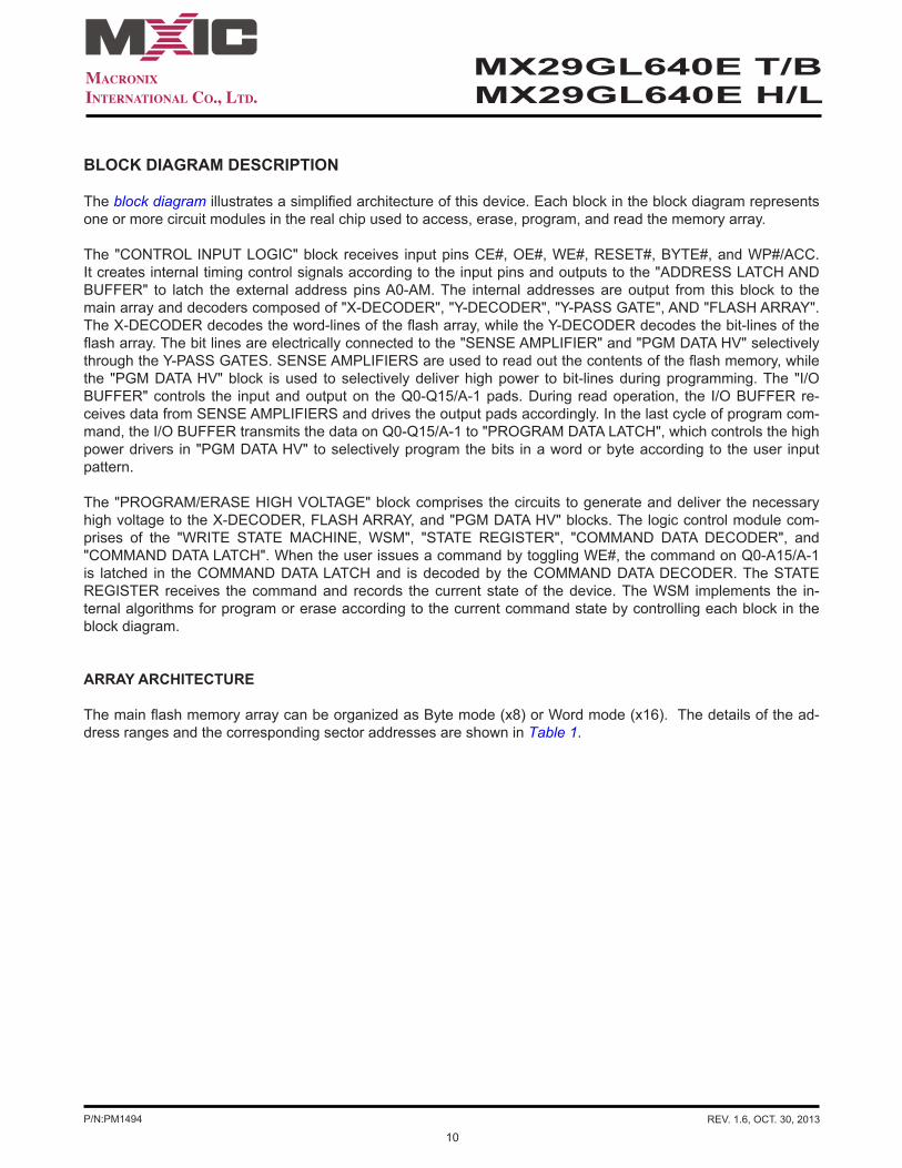
BLOCK DIAGRAM DESCRIPTION The block diagram illustrates a simplified architecture of this device. Each block in the block diagram represents one or more circuit modules in the real chip used to access, erase, program, and read the memory array.
The "CONTROL INPUT LOGIC" block receives input pins CE#, OE#, WE#, RESET#, BYTE#, and WP#/ACC. It creates internal timing control signals according to the input pins and outputs to the "ADDRESS LATCH AND BUFFER" to latch the external address pins A0-AM. The internal addresses are output from this block to the main array and decoders composed of "X-DECODER", "Y-DECODER", "Y-PASS GATE", AND "FLASH ARRAY". The X-DECODER decodes the word-lines of the flash array, while the Y-DECODER decodes the bit-lines of the flash array. The bit lines are electrically connected to the "SENSE AMPLIFIER" and "PGM DATA HV" selectively through the Y-PASS GATES. SENSE AMPLIFIERS are used to read out the contents of the flash memory, while the "PGM DATA HV" block is used to selectively deliver high power to bit-lines during programming. The "I/O BUFFER" controls the input and output on the Q0-Q15/A-1 pads. During read operation, the I/O BUFFER re-ceives data from SENSE AMPLIFIERS and drives the output pads accordingly. In the last cycle of program com-mand, the I/O BUFFER transmits the data on Q0-Q15/A-1 to "PROGRAM DATA LATCH", which controls the high power drivers in "PGM DATA HV" to selectively program the bits in a word or byte according to the user input pattern.
The "PROGRAM/ERASE HIGH VOLTAGE" block comprises the circuits to generate and deliver the necessary high voltage to the X-DECODER, FLASH ARRAY, and "PGM DATA HV" blocks. The logic control module com-prises of the "WRITE STATE MACHINE, WSM", "STATE REGISTER", "COMMAND DATA DECODER", and "COMMAND DATA LATCH". When the user issues a command by toggling WE#, the command on Q0-A15/A-1 is latched in the COMMAND DATA LATCH and is decoded by the COMMAND DATA DECODER. The STATE REGISTER receives the command and records the current state of the device. The WSM implements the in-ternal algorithms for program or erase according to the current command state by controlling each block in the block diagram.
ARRAY ARCHITECTURE The main flash memory array can be organized as Byte mode (x8) or Word mode (x16). The details of the ad-dress ranges and the corresponding sector addresses are shown in Table 1.

11P/N:PM1494 REV. 1.6, OCT. 30, 2013
MX29GL640E T/BMX29GL640E H/L
Table 1-1. MX29GL640ET SECTOR ARCHITECTURE
BLOCK STRUCTURE
Sector SizeSector Sector Address
A21-A12(x8)
Address Range (x16)
Address RangeKbytes Kwords64 32 SA0 0000000xxx 000000h-00FFFFh 000000h-07FFFh64 32 SA1 0000001xxx 010000h-01FFFFh 008000h-0FFFFh64 32 SA2 0000010xxx 020000h-02FFFFh 010000h-17FFFh64 32 SA3 0000011xxx 030000h-03FFFFh 018000h-01FFFFh64 32 SA4 0000100xxx 040000h-04FFFFh 020000h-027FFFh64 32 SA5 0000101xxx 050000h-05FFFFh 028000h-02FFFFh64 32 SA6 0000110xxx 060000h-06FFFFh 030000h-037FFFh64 32 SA7 0000111xxx 070000h-07FFFFh 038000h-03FFFFh64 32 SA8 0001000xxx 080000h-08FFFFh 040000h-047FFFh64 32 SA9 0001001xxx 090000h-09FFFFh 048000h-04FFFFh64 32 SA10 0001010xxx 0A0000h-0AFFFFh 050000h-057FFFh64 32 SA11 0001011xxx 0B0000h-0BFFFFh 058000h-05FFFFh64 32 SA12 0001100xxx 0C0000h-0CFFFFh 060000h-067FFFh64 32 SA13 0001101xxx 0D0000h-0DFFFFh 068000h-06FFFFh64 32 SA14 0001110xxx 0E0000h-0EFFFFh 070000h-077FFFh64 32 SA15 0001111xxx 0F0000h-0FFFFFh 078000h-07FFFFh64 32 SA16 0010000xxx 100000h-10FFFFh 080000h-087FFFh64 32 SA17 0010001xxx 110000h-11FFFFh 088000h-08FFFFh64 32 SA18 0010010xxx 120000h-12FFFFh 090000h-097FFFh64 32 SA19 0010011xxx 130000h-13FFFFh 098000h-09FFFFh64 32 SA20 0010100xxx 140000h-14FFFFh 0A0000h-0A7FFFh64 32 SA21 0010101xxx 150000h-15FFFFh 0A8000h-0AFFFFh64 32 SA22 0010110xxx 160000h-16FFFFh 0B0000h-0B7FFFh64 32 SA23 0010111xxx 170000h-17FFFFh 0B8000h-0BFFFFh64 32 SA24 0011000xxx 180000h-18FFFFh 0C0000h-0C7FFFh64 32 SA25 0011001xxx 190000h-19FFFFh 0C8000h-0CFFFFh64 32 SA26 0011010xxx 1A0000h-1AFFFFh 0D0000h-0D7FFFh64 32 SA27 0011011xxx 1B0000h-1BFFFFh 0D8000h-0DFFFFh64 32 SA28 0011100xxx 1C0000h-1CFFFFh 0E0000h-0E7FFFh64 32 SA29 0011101xxx 1D0000h-1DFFFFh 0E8000h-0EFFFFh64 32 SA30 0011110xxx 1E0000h-1EFFFFh 0F0000h-0F7FFFh64 32 SA31 0011111xxx 1F0000h-1FFFFFh 0F8000h-0FFFFFh64 32 SA32 0100000xxx 200000h-20FFFFh 100000h-107FFFh64 32 SA33 0100001xxx 210000h-21FFFFh 108000h-10FFFFh64 32 SA34 0100010xxx 220000h-22FFFFh 110000h-117FFFh64 32 SA35 0100011xxx 230000h-23FFFFh 118000h-11FFFFh64 32 SA36 0100100xxx 240000h-24FFFFh 120000h-127FFFh64 32 SA37 0100101xxx 250000h-25FFFFh 128000h-12FFFFh64 32 SA38 0100110xxx 260000h-26FFFFh 130000h-137FFFh64 32 SA39 0100111xxx 270000h-27FFFFh 138000h-13FFFFh

12P/N:PM1494 REV. 1.6, OCT. 30, 2013
MX29GL640E T/BMX29GL640E H/L
Sector SizeSector Sector Address
A21-A12(x8)
Address Range (x16)
Address RangeKbytes Kwords64 32 SA40 0101000xxx 280000h-28FFFFh 140000h-147FFFh64 32 SA41 0101001xxx 290000h-29FFFFh 148000h-14FFFFh64 32 SA42 0101010xxx 2A0000h-2AFFFFh 150000h-157FFFh64 32 SA43 0101011xxx 2B0000h-2BFFFFh 158000h-15FFFFh64 32 SA44 0101100xxx 2C0000h-2CFFFFh 160000h-147FFFh64 32 SA45 0101101xxx 2D0000h-2DFFFFh 168000h-14FFFFh64 32 SA46 0101110xxx 2E0000h-2EFFFFh 170000h-177FFFh64 32 SA47 0101111xxx 2F0000h-2FFFFFh 178000h-17FFFFh64 32 SA48 0110000xxx 300000h-30FFFFh 180000h-187FFFh64 32 SA49 0110001xxx 310000h-31FFFFh 188000h-18FFFFh64 32 SA50 0110010xxx 320000h-32FFFFh 190000h-197FFFh64 32 SA51 0110011xxx 330000h-33FFFFh 198000h-19FFFFh64 32 SA52 0110100xxx 340000h-34FFFFh 1A0000h-1A7FFFh64 32 SA53 0110101xxx 350000h-35FFFFh 1A8000h-1AFFFFh64 32 SA54 0110110xxx 360000h-36FFFFh 1B0000h-1B7FFFh64 32 SA55 0110111xxx 370000h-37FFFFh 1B8000h-1BFFFFh64 32 SA56 0111000xxx 380000h-38FFFFh 1C0000h-1C7FFFh64 32 SA57 0111001xxx 390000h-39FFFFh 1C8000h-1CFFFFh64 32 SA58 0111010xxx 3A0000h-3AFFFFh 1D0000h-1D7FFFh64 32 SA59 0111011xxx 3B0000h-3BFFFFh 1D8000h-1DFFFFh64 32 SA60 0111100xxx 3C0000h-3CFFFFh 1E0000h-1E7FFFh64 32 SA61 0111101xxx 3D0000h-3DFFFFh 1E8000h-1EFFFFh64 32 SA62 0111110xxx 3E0000h-3EFFFFh 1F0000h-1F7FFFh64 32 SA63 0111111xxx 3F0000h-3FFFFFh 1F8000h-1FFFFFh64 32 SA64 1000000xxx 400000h-40FFFFh 200000h-207FFFh64 32 SA65 1000001xxx 410000h-41FFFFh 208000h-20FFFFh64 32 SA66 1000010xxx 420000h-42FFFFh 210000h-217FFFh64 32 SA67 1000011xxx 430000h-43FFFFh 218000h-21FFFFh64 32 SA68 1000100xxx 440000h-44FFFFh 220000h-227FFFh64 32 SA69 1000101xxx 450000h-45FFFFh 228000h-22FFFFh64 32 SA70 1000110xxx 460000h-46FFFFh 230000h-237FFFh64 32 SA71 1000111xxx 470000h-47FFFFh 238000h-23FFFFh64 32 SA72 1001000xxx 480000h-48FFFFh 240000h-247FFFh64 32 SA73 1001001xxx 490000h-49FFFFh 248000h-24FFFFh64 32 SA74 1001010xxx 4A0000h-4AFFFFh 250000h-257FFFh64 32 SA75 1001011xxx 4B0000h-4BFFFFh 258000h-25FFFFh64 32 SA76 1001100xxx 4C0000h-4CFFFFh 260000h-247FFFh64 32 SA77 1001101xxx 4D0000h-4DFFFFh 268000h-24FFFFh64 32 SA78 1001110xxx 4E0000h-4EFFFFh 270000h-277FFFh64 32 SA79 1001111xxx 4F0000h-4FFFFFh 278000h-27FFFFh64 32 SA80 1010000xxx 500000h-50FFFFh 280000h-287FFFh64 32 SA81 1010001xxx 510000h-51FFFFh 288000h-28FFFFh64 32 SA82 1010010xxx 520000h-52FFFFh 290000h-297FFFh

13P/N:PM1494 REV. 1.6, OCT. 30, 2013
MX29GL640E T/BMX29GL640E H/L
Sector SizeSector Sector Address
A21-A12(x8)
Address Range (x16)
Address RangeKbytes Kwords64 32 SA83 1010011xxx 530000h-53FFFFh 298000h-29FFFFh64 32 SA84 1010100xxx 540000h-54FFFFh 2A0000h-2A7FFFh64 32 SA85 1010101xxx 550000h-55FFFFh 2A8000h-2AFFFFh64 32 SA86 1010110xxx 560000h-56FFFFh 2B0000h-2B7FFFh64 32 SA87 1010111xxx 570000h-57FFFFh 2B8000h-2BFFFFh64 32 SA88 1011000xxx 580000h-58FFFFh 2C0000h-2C7FFFh64 32 SA89 1011001xxx 590000h-59FFFFh 2C8000h-2CFFFFh64 32 SA90 1011010xxx 5A0000h-5AFFFFh 2D0000h-2D7FFFh64 32 SA91 1011011xxx 5B0000h-5BFFFFh 2D8000h-2DFFFFh64 32 SA92 1011100xxx 5C0000h-5CFFFFh 2E0000h-2E7FFFh64 32 SA93 1011101xxx 5D0000h-5DFFFFh 2E8000h-2EFFFFh64 32 SA94 1011110xxx 5E0000h-5EFFFFh 2F0000h-2F7FFFh64 32 SA95 1011111xxx 5F0000h-5FFFFFh 2F8000h-2FFFFFh64 32 SA96 1100000xxx 600000h-60FFFFh 300000h-307FFFh64 32 SA97 1100001xxx 610000h-61FFFFh 308000h-30FFFFh64 32 SA98 1100010xxx 620000h-62FFFFh 310000h-317FFFh64 32 SA99 1100011xxx 630000h-63FFFFh 318000h-31FFFFh64 32 SA100 1100100xxx 640000h-64FFFFh 320000h-327FFFh64 32 SA101 1100101xxx 650000h-65FFFFh 328000h-32FFFFh64 32 SA102 1100110xxx 660000h-66FFFFh 330000h-337FFFh64 32 SA103 1100111xxx 670000h-67FFFFh 338000h-33FFFFh64 32 SA104 1101000xxx 680000h-68FFFFh 340000h-347FFFh64 32 SA105 1101001xxx 690000h-69FFFFh 348000h-34FFFFh64 32 SA106 1101010xxx 6A0000h-6AFFFFh 350000h-357FFFh64 32 SA107 1101011xxx 6B0000h-6BFFFFh 358000h-35FFFFh64 32 SA108 1101100xxx 6C0000h-6CFFFFh 360000h-347FFFh64 32 SA109 1101101xxx 6D0000h-6DFFFFh 368000h-34FFFFh64 32 SA110 1101110xxx 6E0000h-6EFFFFh 370000h-377FFFh64 32 SA111 1101111xxx 6F0000h-6FFFFFh 378000h-37FFFFh64 32 SA112 1110000xxx 700000h-70FFFFh 380000h-387FFFh64 32 SA113 1110001xxx 710000h-71FFFFh 388000h-38FFFFh64 32 SA114 1110010xxx 720000h-72FFFFh 390000h-397FFFh64 32 SA115 1110011xxx 730000h-73FFFFh 398000h-39FFFFh64 32 SA116 1110100xxx 740000h-74FFFFh 3A0000h-3A7FFFh64 32 SA117 1110101xxx 750000h-75FFFFh 3A8000h-3AFFFFh64 32 SA118 1110110xxx 760000h-76FFFFh 3B0000h-3B7FFFh64 32 SA119 1110111xxx 770000h-77FFFFh 3B8000h-3BFFFFh64 32 SA120 1111000xxx 780000h-78FFFFh 3C0000h-3C7FFFh64 32 SA121 1111001xxx 790000h-79FFFFh 3C8000h-3CFFFFh64 32 SA122 1111010xxx 7A0000h-7AFFFFh 3D0000h-3D7FFFh64 32 SA123 1111011xxx 7B0000h-7BFFFFh 3D8000h-3DFFFFh64 32 SA124 1111100xxx 7C0000h-7CFFFFh 3E0000h-3E7FFFh64 32 SA125 1111101xxx 7D0000h-7DFFFFh 3E8000h-3EFFFFh

14P/N:PM1494 REV. 1.6, OCT. 30, 2013
MX29GL640E T/BMX29GL640E H/L
Sector SizeSector Sector Address
A21-A12(x8)
Address Range (x16)
Address RangeKbytes Kwords64 32 SA126 1111110xxx 7E0000h-7EFFFFh 3F0000h-3F7FFFh8 4 SA127 1111111000 7F0000h-7F1FFFh 3F8000h-3FFFFFh8 4 SA128 1111111001 7F2000h-7F3FFFh 3F9000h-3F9FFFh8 4 SA129 1111111010 7F4000h-7F5FFFh 3FA000h-3FAFFFh8 4 SA130 1111111011 7F6000h-7F7FFFh 3FB000h-3FBFFFh8 4 SA131 1111111100 7F8000h-7F9FFFh 3FC000h-3FCFFFh8 4 SA132 1111111101 7FA000h-7FBFFFh 3FD000h-3FDFFFh8 4 SA133 1111111110 7FC000h-7FDFFFh 3FE000h-3FEFFFh8 4 SA134 1111111111 7FE000h-7FFFFFh 3FF000h-3FFFFFh

15P/N:PM1494 REV. 1.6, OCT. 30, 2013
MX29GL640E T/BMX29GL640E H/L
Sector SizeSector Sector Address
A21-A12(x8)
Address Range (x16)
Address RangeKbytes Kwords8 4 SA0 0000000000 000000h-001FFFh 000000h-000FFFh8 4 SA1 0000000001 002000h-003FFFh 001000h-001FFFh8 4 SA2 0000000010 004000h-005FFFh 002000h-002FFFh8 4 SA3 0000000011 006000h-007FFFh 003000h-003FFFh8 4 SA4 0000000100 008000h-009FFFh 004000h-004FFFh8 4 SA5 0000000101 00A000h-00BFFFh 005000h-005FFFh8 4 SA6 0000000110 00C000h-00DFFFh 006000h-006FFFh8 4 SA7 0000000111 00E000h-00FFFFh 007000h-007FFFh
64 32 SA8 0000001xxx 010000h-01FFFFh 008000h-00FFFFh64 32 SA9 0000010xxx 020000h-02FFFFh 010000h-017FFFh64 32 SA10 0000011xxx 030000h-03FFFFh 018000h-01FFFFh64 32 SA11 0000100xxx 040000h-04FFFFh 020000h-027FFFh64 32 SA12 0000101xxx 050000h-05FFFFh 028000h-02FFFFh64 32 SA13 0000110xxx 060000h-06FFFFh 030000h-037FFFh64 32 SA14 0000111xxx 070000h-07FFFFh 038000h-03FFFFh64 32 SA15 0001000xxx 080000h-08FFFFh 040000h-047FFFh64 32 SA16 0001001xxx 090000h-09FFFFh 048000h-04FFFFh64 32 SA17 0001010xxx 0A0000h-0AFFFFh 050000h-057FFFh64 32 SA18 0001011xxx 0B0000h-0BFFFFh 058000h-05FFFFh64 32 SA19 0001100xxx 0C0000h-0CFFFFh 060000h-067FFFh64 32 SA20 0001101xxx 0D0000h-0DFFFFh 068000h-06FFFFh64 32 SA21 0001110xxx 0E0000h-0EFFFFh 070000h-077FFFh64 32 SA22 0001111xxx 0F0000h-0FFFFFh 078000h-07FFFFh64 32 SA23 0010000xxx 100000h-10FFFFh 080000h-087FFFh64 32 SA24 0010001xxx 110000h-11FFFFh 088000h-08FFFFh64 32 SA25 0010010xxx 120000h-12FFFFh 090000h-097FFFh64 32 SA26 0010011xxx 130000h-13FFFFh 098000h-09FFFFh64 32 SA27 0010100xxx 140000h-14FFFFh 0A0000h-0A7FFFh64 32 SA28 0010101xxx 150000h-15FFFFh 0A8000h-0AFFFFh64 32 SA29 0010110xxx 160000h-16FFFFh 0B0000h-0B7FFFh64 32 SA30 0010111xxx 170000h-17FFFFh 0B8000h-0BFFFFh64 32 SA31 0011000xxx 180000h-18FFFFh 0C0000h-0C7FFFh64 32 SA32 0011001xxx 190000h-19FFFFh 0C8000h-0CFFFFh64 32 SA33 0011010xxx 1A0000h-1AFFFFh 0D0000h-0D7FFFh64 32 SA34 0011011xxx 1B0000h-1BFFFFh 0D8000h-0DFFFFh64 32 SA35 0011100xxx 1C0000h-1CFFFFh 0E0000h-0E7FFFh64 32 SA36 0011101xxx 1D0000h-1DFFFFh 0E8000h-0EFFFFh64 32 SA37 0011110xxx 1E0000h-1EFFFFh 0F0000h-0F7FFFh64 32 SA38 0011111xxx 1F0000h-1FFFFFh 0F8000h-0FFFFFh64 32 SA39 0100000xxx 200000h-20FFFFh 100000h-107FFFh64 32 SA40 0100001xxx 210000h-21FFFFh 108000h-10FFFFh
Table 1-2. MX29GL640EB SECTOR ARCHITECTURE

16P/N:PM1494 REV. 1.6, OCT. 30, 2013
MX29GL640E T/BMX29GL640E H/L
Sector SizeSector Sector Address
A21-A12(x8)
Address Range (x16)
Address RangeKbytes Kwords64 32 SA41 0100010xxx 220000h-22FFFFh 110000h-117FFFh64 32 SA42 0100011xxx 230000h-23FFFFh 118000h-11FFFFh64 32 SA43 0100100xxx 240000h-24FFFFh 120000h-127FFFh64 32 SA44 0100101xxx 250000h-25FFFFh 128000h-12FFFFh64 32 SA45 0100110xxx 260000h-26FFFFh 130000h-137FFFh64 32 SA46 0100111xxx 270000h-27FFFFh 138000h-13FFFFh64 32 SA47 0101000xxx 280000h-28FFFFh 140000h-147FFFh64 32 SA48 0101001xxx 290000h-29FFFFh 148000h-14FFFFh64 32 SA49 0101010xxx 2A0000h-2AFFFFh 150000h-157FFFh64 32 SA50 0101011xxx 2B0000h-2BFFFFh 158000h-15FFFFh64 32 SA51 0101100xxx 2C0000h-2CFFFFh 160000h-167FFFh64 32 SA52 0101101xxx 2D0000h-2DFFFFh 168000h-16FFFFh64 32 SA53 0101110xxx 2E0000h-2EFFFFh 170000h-177FFFh64 32 SA54 0101111xxx 2F0000h-2FFFFFh 178000h-17FFFFh64 32 SA55 0110000xxx 300000h-30FFFFh 180000h-187FFFh64 32 SA56 0110001xxx 310000h-31FFFFh 188000h-18FFFFh64 32 SA57 0110010xxx 320000h-32FFFFh 190000h-197FFFh64 32 SA58 0110011xxx 330000h-33FFFFh 198000h-19FFFFh64 32 SA59 0110100xxx 340000h-34FFFFh 1A0000h-1A7FFFh64 32 SA60 0110101xxx 350000h-35FFFFh 1A8000h-1AFFFFh64 32 SA61 0110110xxx 360000h-36FFFFh 1B0000h-1B7FFFh64 32 SA62 0110111xxx 370000h-37FFFFh 1B8000h-1BFFFFh64 32 SA63 0111000xxx 380000h-38FFFFh 1C0000h-1C7FFFh64 32 SA64 0111001xxx 390000h-39FFFFh 1C8000h-1CFFFFh64 32 SA65 0111010xxx 3A0000h-3AFFFFh 1D0000h-1D7FFFh64 32 SA66 0111011xxx 3B0000h-3BFFFFh 1D8000h-1DFFFFh64 32 SA67 0111100xxx 3C0000h-3CFFFFh 1E0000h-1E7FFFh64 32 SA68 0111101xxx 3D0000h-3DFFFFh 1E8000h-1EFFFFh64 32 SA69 0111110xxx 3E0000h-3EFFFFh 1F0000h-1F7FFFh64 32 SA70 0111111xxx 3F0000h-3FFFFFh 1F8000h-1FFFFFh64 32 SA71 1000000xxx 400000h-40FFFFh 200000h-207FFFh64 32 SA72 1000001xxx 410000h-41FFFFh 208000h-20FFFFh64 32 SA73 1000010xxx 420000h-42FFFFh 210000h-217FFFh64 32 SA74 1000011xxx 430000h-43FFFFh 218000h-21FFFFh64 32 SA75 1000100xxx 440000h-44FFFFh 220000h-227FFFh64 32 SA76 1000101xxx 450000h-45FFFFh 228000h-22FFFFh64 32 SA77 1000110xxx 460000h-46FFFFh 230000h-237FFFh64 32 SA78 1000111xxx 470000h-47FFFFh 238000h-23FFFFh64 32 SA79 1001000xxx 480000h-48FFFFh 240000h-247FFFh64 32 SA80 1001001xxx 490000h-49FFFFh 248000h-24FFFFh64 32 SA81 1001010xxx 4A0000h-4AFFFFh 250000h-257FFFh64 32 SA82 1001011xxx 4B0000h-4BFFFFh 258000h-25FFFFh

17P/N:PM1494 REV. 1.6, OCT. 30, 2013
MX29GL640E T/BMX29GL640E H/L
Sector SizeSector Sector Address
A21-A12(x8)
Address Range (x16)
Address RangeKbytes Kwords64 32 SA83 1001100xxx 4C0000h-4CFFFFh 260000h-267FFFh64 32 SA84 1001101xxx 4D0000h-4DFFFFh 268000h-26FFFFh64 32 SA85 1001110xxx 4E0000h-4EFFFFh 270000h-277FFFh64 32 SA86 1001111xxx 4F0000h-4FFFFFh 278000h-27FFFFh64 32 SA87 1010000xxx 500000h-50FFFFh 280000h-287FFFh64 32 SA88 1010001xxx 510000h-51FFFFh 288000h-28FFFFh64 32 SA89 1010010xxx 520000h-52FFFFh 290000h-297FFFh64 32 SA90 1010011xxx 530000h-53FFFFh 298000h-29FFFFh64 32 SA91 1010100xxx 540000h-54FFFFh 2A0000h-2A7FFFh64 32 SA92 1010101xxx 550000h-55FFFFh 2A8000h-2AFFFFh64 32 SA93 1010110xxx 560000h-56FFFFh 2B0000h-2B7FFFh64 32 SA94 1010111xxx 570000h-57FFFFh 2B8000h-2BFFFFh64 32 SA95 1011000xxx 580000h-58FFFFh 2C0000h-2C7FFFh64 32 SA96 1011001xxx 590000h-59FFFFh 2C8000h-2CFFFFh64 32 SA97 1011010xxx 5A0000h-5AFFFFh 2D0000h-2D7FFFh64 32 SA98 1011011xxx 5B0000h-5BFFFFh 2D8000h-2DFFFFh64 32 SA99 1011100xxx 5C0000h-5CFFFFh 2E0000h-2E7FFFh64 32 SA100 1011101xxx 5D0000h-5DFFFFh 2E8000h-2EFFFFh64 32 SA101 1011110xxx 5E0000h-5EFFFFh 2F0000h-2F7FFFh64 32 SA102 1011111xxx 5F0000h-5FFFFFh 2F8000h-2FFFFFh64 32 SA103 1100000xxx 600000h-60FFFFh 300000h-307FFFh64 32 SA104 1100001xxx 610000h-61FFFFh 308000h-30FFFFh64 32 SA105 1100010xxx 620000h-62FFFFh 310000h-317FFFh64 32 SA106 1100011xxx 630000h-63FFFFh 318000h-31FFFFh64 32 SA107 1100100xxx 640000h-64FFFFh 320000h-327FFFh64 32 SA108 1100101xxx 650000h-65FFFFh 328000h-32FFFFh64 32 SA109 1100110xxx 660000h-66FFFFh 330000h-337FFFh64 32 SA110 1100111xxx 670000h-67FFFFh 338000h-33FFFFh64 32 SA111 1101000xxx 680000h-68FFFFh 340000h-347FFFh64 32 SA112 1101001xxx 690000h-69FFFFh 348000h-34FFFFh64 32 SA113 1101010xxx 6A0000h-6AFFFFh 350000h-357FFFh64 32 SA114 1101011xxx 6B0000h-6BFFFFh 358000h-35FFFFh64 32 SA115 1101100xxx 6C0000h-6CFFFFh 360000h-367FFFh64 32 SA116 1101101xxx 6D0000h-6DFFFFh 368000h-36FFFFh64 32 SA117 1101110xxx 6E0000h-6EFFFFh 370000h-377FFFh64 32 SA118 1101111xxx 6F0000h-6FFFFFh 378000h-37FFFFh64 32 SA119 1110000xxx 700000h-70FFFFh 380000h-387FFFh64 32 SA120 1110001xxx 710000h-71FFFFh 388000h-38FFFFh64 32 SA121 1110010xxx 720000h-72FFFFh 390000h-397FFFh64 32 SA122 1110011xxx 730000h-73FFFFh 398000h-39FFFFh64 32 SA123 1110100xxx 740000h-74FFFFh 3A0000h-3A7FFFh64 32 SA124 1110101xxx 750000h-75FFFFh 3A8000h-3AFFFFh

18P/N:PM1494 REV. 1.6, OCT. 30, 2013
MX29GL640E T/BMX29GL640E H/L
Sector SizeSector Sector Address
A21-A12(x8)
Address Range (x16)
Address RangeKbytes Kwords64 32 SA125 1110110xxx 760000h-76FFFFh 3B0000h-3B7FFFh64 32 SA126 1110111xxx 770000h-77FFFFh 3B8000h-3BFFFFh64 32 SA127 1111000xxx 780000h-78FFFFh 3C0000h-3C7FFFh64 32 SA128 1111001xxx 790000h-79FFFFh 3C8000h-3CFFFFh64 32 SA129 1111010xxx 7A0000h-7AFFFFh 3D0000h-3D7FFFh64 32 SA130 1111011xxx 7B0000h-7BFFFFh 3D8000h-3DFFFFh64 32 SA131 1111100xxx 7C0000h-7CFFFFh 3E0000h-3E7FFFh64 32 SA132 1111101xxx 7D0000h-7DFFFFh 3E8000h-3EFFFFh64 32 SA133 1111110xxx 7E0000h-7EFFFFh 3F0000h-3F7FFFh64 32 SA134 1111111xxx 7F0000h-7FFFFFh 3F8000h-3FFFFFh
19P/N:PM1494 REV. 1.6, OCT. 30, 2013
MX29GL640E T/BMX29GL640E H/L
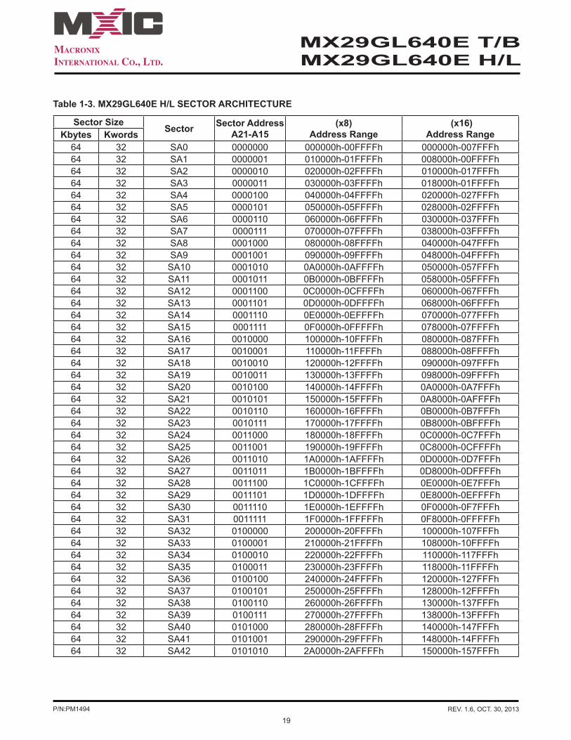
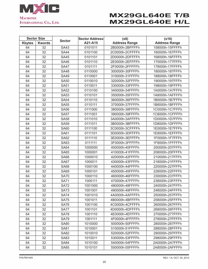
Table 1-3. MX29GL640E H/L SECTOR ARCHITECTURE
Sector SizeSector Sector Address
A21-A15(x8)
Address Range (x16)
Address RangeKbytes Kwords64 32 SA0 0000000 000000h-00FFFFh 000000h-007FFFh64 32 SA1 0000001 010000h-01FFFFh 008000h-00FFFFh64 32 SA2 0000010 020000h-02FFFFh 010000h-017FFFh64 32 SA3 0000011 030000h-03FFFFh 018000h-01FFFFh64 32 SA4 0000100 040000h-04FFFFh 020000h-027FFFh64 32 SA5 0000101 050000h-05FFFFh 028000h-02FFFFh64 32 SA6 0000110 060000h-06FFFFh 030000h-037FFFh64 32 SA7 0000111 070000h-07FFFFh 038000h-03FFFFh64 32 SA8 0001000 080000h-08FFFFh 040000h-047FFFh64 32 SA9 0001001 090000h-09FFFFh 048000h-04FFFFh64 32 SA10 0001010 0A0000h-0AFFFFh 050000h-057FFFh64 32 SA11 0001011 0B0000h-0BFFFFh 058000h-05FFFFh64 32 SA12 0001100 0C0000h-0CFFFFh 060000h-067FFFh64 32 SA13 0001101 0D0000h-0DFFFFh 068000h-06FFFFh64 32 SA14 0001110 0E0000h-0EFFFFh 070000h-077FFFh64 32 SA15 0001111 0F0000h-0FFFFFh 078000h-07FFFFh64 32 SA16 0010000 100000h-10FFFFh 080000h-087FFFh64 32 SA17 0010001 110000h-11FFFFh 088000h-08FFFFh64 32 SA18 0010010 120000h-12FFFFh 090000h-097FFFh64 32 SA19 0010011 130000h-13FFFFh 098000h-09FFFFh64 32 SA20 0010100 140000h-14FFFFh 0A0000h-0A7FFFh64 32 SA21 0010101 150000h-15FFFFh 0A8000h-0AFFFFh64 32 SA22 0010110 160000h-16FFFFh 0B0000h-0B7FFFh64 32 SA23 0010111 170000h-17FFFFh 0B8000h-0BFFFFh64 32 SA24 0011000 180000h-18FFFFh 0C0000h-0C7FFFh64 32 SA25 0011001 190000h-19FFFFh 0C8000h-0CFFFFh64 32 SA26 0011010 1A0000h-1AFFFFh 0D0000h-0D7FFFh64 32 SA27 0011011 1B0000h-1BFFFFh 0D8000h-0DFFFFh64 32 SA28 0011100 1C0000h-1CFFFFh 0E0000h-0E7FFFh64 32 SA29 0011101 1D0000h-1DFFFFh 0E8000h-0EFFFFh64 32 SA30 0011110 1E0000h-1EFFFFh 0F0000h-0F7FFFh64 32 SA31 0011111 1F0000h-1FFFFFh 0F8000h-0FFFFFh64 32 SA32 0100000 200000h-20FFFFh 100000h-107FFFh64 32 SA33 0100001 210000h-21FFFFh 108000h-10FFFFh64 32 SA34 0100010 220000h-22FFFFh 110000h-117FFFh64 32 SA35 0100011 230000h-23FFFFh 118000h-11FFFFh64 32 SA36 0100100 240000h-24FFFFh 120000h-127FFFh64 32 SA37 0100101 250000h-25FFFFh 128000h-12FFFFh64 32 SA38 0100110 260000h-26FFFFh 130000h-137FFFh64 32 SA39 0100111 270000h-27FFFFh 138000h-13FFFFh64 32 SA40 0101000 280000h-28FFFFh 140000h-147FFFh64 32 SA41 0101001 290000h-29FFFFh 148000h-14FFFFh64 32 SA42 0101010 2A0000h-2AFFFFh 150000h-157FFFh
20P/N:PM1494 REV. 1.6, OCT. 30, 2013
MX29GL640E T/BMX29GL640E H/L
Sector SizeSector Sector Address
A21-A15(x8)
Address Range (x16)
Address RangeKbytes Kwords64 32 SA43 0101011 2B0000h-2BFFFFh 158000h-15FFFFh64 32 SA44 0101100 2C0000h-2CFFFFh 160000h-167FFFh64 32 SA45 0101101 2D0000h-2DFFFFh 168000h-16FFFFh64 32 SA46 0101110 2E0000h-2EFFFFh 170000h-177FFFh64 32 SA47 0101111 2F0000h-2FFFFFh 178000h-17FFFFh64 32 SA48 0110000 300000h-30FFFFh 180000h-187FFFh64 32 SA49 0110001 310000h-31FFFFh 188000h-18FFFFh64 32 SA50 0110010 320000h-32FFFFh 190000h-197FFFh64 32 SA51 0110011 330000h-33FFFFh 198000h-19FFFFh64 32 SA52 0110100 340000h-34FFFFh 1A0000h-1A7FFFh64 32 SA53 0110101 350000h-35FFFFh 1A8000h-1AFFFFh64 32 SA54 0110110 360000h-36FFFFh 1B0000h-1B7FFFh64 32 SA55 0110111 370000h-37FFFFh 1B8000h-1BFFFFh64 32 SA56 0111000 380000h-38FFFFh 1C0000h-1C7FFFh64 32 SA57 0111001 390000h-39FFFFh 1C8000h-1CFFFFh64 32 SA58 0111010 3A0000h-3AFFFFh 1D0000h-1D7FFFh64 32 SA59 0111011 3B0000h-3BFFFFh 1D8000h-1DFFFFh64 32 SA60 0111100 3C0000h-3CFFFFh 1E0000h-1E7FFFh64 32 SA61 0111101 3D0000h-3DFFFFh 1E8000h-1EFFFFh64 32 SA62 0111110 3E0000h-3EFFFFh 1F0000h-1F7FFFh64 32 SA63 0111111 3F0000h-3FFFFFh 1F8000h-1FFFFFh64 32 SA64 1000000 400000h-40FFFFh 200000h-207FFFh64 32 SA65 1000001 410000h-41FFFFh 208000h-20FFFFh64 32 SA66 1000010 420000h-42FFFFh 210000h-217FFFh64 32 SA67 1000011 430000h-43FFFFh 218000h-21FFFFh64 32 SA68 1000100 440000h-44FFFFh 220000h-227FFFh64 32 SA69 1000101 450000h-45FFFFh 228000h-22FFFFh64 32 SA70 1000110 460000h-46FFFFh 230000h-237FFFh64 32 SA71 1000111 470000h-47FFFFh 238000h-23FFFFh64 32 SA72 1001000 480000h-48FFFFh 240000h-247FFFh64 32 SA73 1001001 490000h-49FFFFh 248000h-24FFFFh64 32 SA74 1001010 4A0000h-4AFFFFh 250000h-257FFFh64 32 SA75 1001011 4B0000h-4BFFFFh 258000h-25FFFFh64 32 SA76 1001100 4C0000h-4CFFFFh 260000h-267FFFh64 32 SA77 1001101 4D0000h-4DFFFFh 268000h-26FFFFh64 32 SA78 1001110 4E0000h-4EFFFFh 270000h-277FFFh64 32 SA79 1001111 4F0000h-4FFFFFh 278000h-27FFFFh64 32 SA80 1010000 500000h-50FFFFh 280000h-287FFFh64 32 SA81 1010001 510000h-51FFFFh 288000h-28FFFFh64 32 SA82 1010010 520000h-52FFFFh 290000h-297FFFh64 32 SA83 1010011 530000h-53FFFFh 298000h-29FFFFh64 32 SA84 1010100 540000h-54FFFFh 2A0000h-2A7FFFh64 32 SA85 1010101 550000h-55FFFFh 2A8000h-2AFFFFh

21P/N:PM1494 REV. 1.6, OCT. 30, 2013
MX29GL640E T/BMX29GL640E H/L
Sector SizeSector Sector Address
A21-A15(x8)
Address Range (x16)
Address RangeKbytes Kwords64 32 SA86 1010110 560000h-56FFFFh 2B0000h-2B7FFFh64 32 SA87 1010111 570000h-57FFFFh 2B8000h-2BFFFFh64 32 SA88 1011000 580000h-58FFFFh 2C0000h-2C7FFFh64 32 SA89 1011001 590000h-59FFFFh 2C8000h-2CFFFFh64 32 SA90 1011010 5A0000h-5AFFFFh 2D0000h-2D7FFFh64 32 SA91 1011011 5B0000h-5BFFFFh 2D8000h-2DFFFFh64 32 SA92 1011100 5C0000h-5CFFFFh 2E0000h-2E7FFFh64 32 SA93 1011101 5D0000h-5DFFFFh 2E8000h-2EFFFFh64 32 SA94 1011110 5E0000h-5EFFFFh 2F0000h-2F7FFFh64 32 SA95 1011111 5F0000h-5FFFFFh 2F8000h-2FFFFFh64 32 SA96 1100000 600000h-60FFFFh 300000h-307FFFh64 32 SA97 1100001 610000h-61FFFFh 308000h-30FFFFh64 32 SA98 1100010 620000h-62FFFFh 310000h-317FFFh64 32 SA99 1100011 630000h-63FFFFh 318000h-31FFFFh64 32 SA100 1100100 640000h-64FFFFh 320000h-327FFFh64 32 SA101 1100101 650000h-65FFFFh 328000h-32FFFFh64 32 SA102 1100110 660000h-66FFFFh 330000h-337FFFh64 32 SA103 1100111 670000h-67FFFFh 338000h-33FFFFh64 32 SA104 1101000 680000h-68FFFFh 340000h-347FFFh64 32 SA105 1101001 690000h-69FFFFh 348000h-34FFFFh64 32 SA106 1101010 6A0000h-6AFFFFh 350000h-357FFFh64 32 SA107 1101011 6B0000h-6BFFFFh 358000h-35FFFFh64 32 SA108 1101100 6C0000h-6CFFFFh 360000h-367FFFh64 32 SA109 1101101 6D0000h-6DFFFFh 368000h-36FFFFh64 32 SA110 1101110 6E0000h-6EFFFFh 370000h-377FFFh64 32 SA111 1101111 6F0000h-6FFFFFh 378000h-37FFFFh64 32 SA112 1110000 700000h-70FFFFh 380000h-387FFFh64 32 SA113 1110001 710000h-71FFFFh 388000h-38FFFFh64 32 SA114 1110010 720000h-72FFFFh 390000h-397FFFh64 32 SA115 1110011 730000h-73FFFFh 398000h-39FFFFh64 32 SA116 1110100 740000h-74FFFFh 3A0000h-3A7FFFh64 32 SA117 1110101 750000h-75FFFFh 3A8000h-3AFFFFh64 32 SA118 1110110 760000h-76FFFFh 3B0000h-3B7FFFh64 32 SA119 1110111 770000h-77FFFFh 3B8000h-3BFFFFh64 32 SA120 1111000 780000h-78FFFFh 3C0000h-3C7FFFh64 32 SA121 1111001 790000h-79FFFFh 3C8000h-3CFFFFh64 32 SA122 1111010 7A0000h-7AFFFFh 3D0000h-3D7FFFh64 32 SA123 1111011 7B0000h-7BFFFFh 3D8000h-3DFFFFh64 32 SA124 1111100 7C0000h-7CFFFFh 3E0000h-3E7FFFh64 32 SA125 1111101 7D0000h-7DFFFFh 3E8000h-3EFFFFh64 32 SA126 1111110 7E0000h-7EFFFFh 3F0000h-3F7FFFh64 32 SA127 1111111 7F0000h-7FFFFFh 3F8000h-3FFFFFh

22P/N:PM1494 REV. 1.6, OCT. 30, 2013
MX29GL640E T/BMX29GL640E H/L
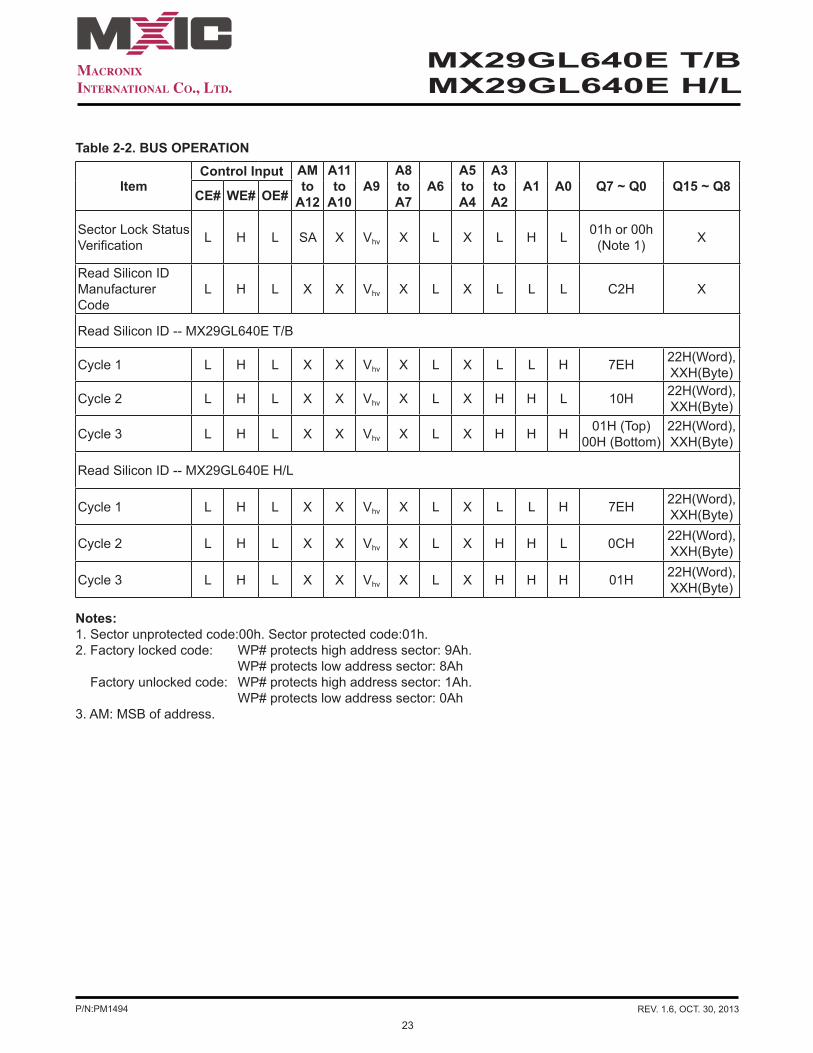
Table 2-1. BUS OPERATION
Notes:1. MX29GL640E T/B: Protect Top or Bottom two sectors if WP#/ACC=Vil. MX29GL640E H/L: Protect first or last sector if WP#/ACC=Vil.2. When WP#/ACC = Vih, the protection conditions of the outmost sector depends on previous protection condi-
tions. Refer to the advanced protect feature.3. Q0~Q15 are input (DIN) or output (DOUT) pins according to the requests of command sequence, sector pro-
tection, or data polling algorithm.4. In Word Mode (Byte#=Vih), the addresses are AM to A0, AM: MSB of address. In Byte Mode (Byte#=Vil), the addresses are AM to A-1 (Q15), AM: MSB of address.
Mode Select RE- SET# CE# WE# OE# Address
(Note4)
Data I/O
Q7~Q0
Byte#WP#/ ACC
Vil VihData (I/O) Q15~Q8
Device Reset L X X X X HighZ HighZ HighZ L/H
Standby Mode Vcc ± 0.3V
Vcc± 0.3V X X X HighZ HighZ HighZ H
Output Disable H L H H X HighZ HighZ HighZ L/HRead Mode H L H L AIN DOUT Q8-Q14=
HighZ,Q15=A1
DOUT L/HWrite H L L H AIN DIN DIN Note1,2Accelerate Program H L L H AIN DIN DIN Vhv
BUS OPERATION
23P/N:PM1494 REV. 1.6, OCT. 30, 2013
MX29GL640E T/BMX29GL640E H/L
Notes:1. Sector unprotected code:00h. Sector protected code:01h.2. Factory locked code: WP# protects high address sector: 9Ah. WP# protects low address sector: 8Ah Factory unlocked code: WP# protects high address sector: 1Ah. WP# protects low address sector: 0Ah3. AM: MSB of address.
Table 2-2. BUS OPERATION
ItemControl Input AM
to A12
A11 to
A10A9
A8 to A7
A6A5 to A4
A3 to A2
A1 A0 Q7 ~ Q0 Q15 ~ Q8CE# WE# OE#
Sector Lock Status Verification L H L SA X Vhv X L X L H L 01h or 00h
(Note 1) X
Read Silicon ID Manufacturer Code
L H L X X Vhv X L X L L L C2H X
Read Silicon ID -- MX29GL640E T/B
Cycle 1 L H L X X Vhv X L X L L H 7EH 22H(Word), XXH(Byte)
Cycle 2 L H L X X Vhv X L X H H L 10H 22H(Word), XXH(Byte)
Cycle 3 L H L X X Vhv X L X H H H 01H (Top)00H (Bottom)
22H(Word), XXH(Byte)
Read Silicon ID -- MX29GL640E H/L
Cycle 1 L H L X X Vhv X L X L L H 7EH 22H(Word), XXH(Byte)
Cycle 2 L H L X X Vhv X L X H H L 0CH 22H(Word), XXH(Byte)
Cycle 3 L H L X X Vhv X L X H H H 01H 22H(Word), XXH(Byte)
24P/N:PM1494 REV. 1.6, OCT. 30, 2013
MX29GL640E T/BMX29GL640E H/L
FUNCTIONAL OPERATION DESCRIPTION
READ OPERATION To perform a read operation, the system addresses the desired memory array or status register location by pro-viding its address on the address pins and simultaneously enabling the chip by driving CE# & OE# LOW, and WE# HIGH. After the Tce and Toe timing requirements have been met, the system can read the contents of the addressed location by reading the Data (I/O) pins. If either the CE# or OE# is held HIGH, the outputs will remain tri-stated and no data will appear on the output pins.
PAGE READ
This device is able to conduct MXIC MaskROM compatible high performance page read. Page size is 16 bytes or 8 words. The higher address Amax ~ A3 select the certain page, while A2~A0 for word mode, A2~A-1 for byte mode select the particular word or byte in a page. The page access time is Taa or Tce, following by Tpa for the rest of the page read time. When CE# toggles, access time is Taa or Tce. Page mode can be turned on by keeping "page-read address" constant and changing the "intra-read page" addresses.
WRITE OPERATION
To perform a write operation, the system provides the desired address on the address pins, enables the chip by asserting CE# LOW, and disables the Data (I/O) pins by holding OE# HIGH. The system then places data to be written on the Data (I/O) pins and pulses WE# LOW. The device captures the address information on the falling edge of WE# and the data on the rising edge of WE#. To see an example, please refer to the timing diagram in Figure 4. The system is not allowed to write invalid commands (commands not defined in this datasheet) to the device. Writing an invalid command may put the device in an undefined state.
DEVICE RESET
Driving the RESET# pin LOW for a period of Trp or more will return the device to Read mode. If the device is in the middle of a program or erase operation, the reset operation will take at most a period of Tready1 before the device returns to Read mode. Until the device does returns to Read mode, the RY/BY# pin will remain Low (Busy Status).
When the RESET# pin is held at GND±0.3V, the device only consumes standby (Isbr) current. However, the de-vice draws larger current if the RESET# pin is held at a voltage greater than GND+0.3V and less than or equal to Vil.
It is recommended to tie the system reset signal to the RESET# pin of the flash memory. This allows the device to be reset with the system and puts it in a state where the system can immediately begin reading boot code from it.
STANDBY MODE
The device enters Standby mode whenever the RESET# and CE# pins are both held High except in the embed-ded mode. While in this mode, WE# and OE# will be ignored, all Data Output pins will be in a high impedance state, and the device will draw minimal (Isb) current.

25P/N:PM1494 REV. 1.6, OCT. 30, 2013
MX29GL640E T/BMX29GL640E H/L
FUNCTIONAL OPERATION DESCRIPTION (cont'd)
OUTPUT DISABLE
While in active mode (RESET# HIGH and CE# LOW), the OE# pin controls the state of the output pins. If OE# is held HIGH, all Data (I/O) pins will remain tri-stated. If held LOW, the Byte or Word Data (I/O) pins will drive data.
BYTE/WORD SELECTION
The BYTE# input pin is used to select the organization of the array data and how the data is input/output on the Data (I/O) pins. If the BYTE# pin is held HIGH, Word mode will be selected and all 16 data lines (Q0 to Q15) will be active.
If BYTE# is forced LOW, Byte mode will be active and only data lines Q0 to Q7 will be active. Data lines Q8 to Q14 will remain in a high impedance state and Q15 becomes the A-1 address input pin.
HARDWARE WRITE PROTECT
By driving the WP#/ACC pin LOW. The Top or Bottom two sectors (for MX29GL640E T/B) and the highest or low-est sector (for MX29GL640E H/L) was protected from all erase/program operations. If WP#/ACC is held HIGH (Vih to VCC), these sectors revert to their previously protected/unprotected status.
ACCELERATED PROGRAMMING OPERATION
By applying high voltage (Vhv) to the WP#/ACC pin, the device will enter the Accelerated Programming mode. This mode permits the system to skip the normal command unlock sequences and program byte/word locations directly. During accelerated programming, the current drawn from the WP#/ACC pin is no more than ICP1.
WRITE BUFFER PROGRAMMING OPERATION
Programs 32bytes/16words in a programming operation. To trigger the Write Buffer Programming, start by the first two unlock cycles, then third cycle writes the Write Buffer Load command at the destined programming Sec-tor Address. The forth cycle writes the "word locations subtract one" number.
Following above operations, system starts to write the mingling of address and data. After the programming of the first address or data, the "write-buffer-page" is selected. The following data should be within the above men-tioned page.
The "write-buffer-page" is selected by choosing address Amax-A4.
"Write-Buffer-Page" address has to be the same for all address/ data write into the write buffer. If not, operation will ABORT.
To program the content of the write buffer page this command must be followed by a write to buffer Program con-firm command.
The operation of write-buffer can be suspended or resumed by the standard commands, once the write buffer programming operation is finished, it’ll return to normal READ mode.

26P/N:PM1494 REV. 1.6, OCT. 30, 2013
MX29GL640E T/BMX29GL640E H/L
FUNCTIONAL OPERATION DESCRIPTION (cont'd)
WRITE BUFFER PROGRAMMING OPERATION (cont'd)
ABORT will be executed for the Write Buffer Programming Sequence if following condition occurs:• The value loaded is bigger than the page buffer size during "Number of Locations to Program"• Address written in a sector is not the same as the one assigned during the Write-Buffer-Load command.• Address/ Data pair written to a different write-buffer-page than the one assigned by the "Starting Address"
during the "write buffer data loading" operation.• Writing not "Confirm Command" after the assigned number of "data load" cycles.
At Write Buffer Abort mode, the status register will be Q1=1, Q7=DATA# (last address written), Q6=toggle. A Write-to-Buffer-Abort Reset command sequence has to be written to reset the device for the next operation.
Write buffer programming can be conducted in any sequence. However the CFI functions, autoselect, Secured Silicon sector are not functional when program operation is in progress. Multiple write buffer programming opera-tions on the same write buffer address range without intervening erases is available. Any bit in a write buffer ad-dress range can’t be programmed from 0 back to 1.
SECTOR PROTECT OPERATION
The device provides user programmable protection operations for selected sectors. Please refer to Table 1 which show all Sector assignments.
During the protection operation, the sector address of any sector may be used to specify the Sector being pro-tected.
AUTOMATIC SELECT BUS OPERATIONS
The following five bus operations require A9 to be raised to Vhv. Please see AUTOMATIC SELECT COMMAND SEQUENCE in the COMMAND OPERATIONS section for details of equivalent command operations that do not require the use of Vhv.
SECTOR LOCK STATUS VERIFICATION
To determine the protected state of any sector using bus operations, the system performs a READ OPERATION with A9 raised to Vhv, the sector address applied to address pins A21 to A12, address pins A6, A3, A2 & A0 held LOW, and address pin A1 held HIGH. If data bit Q0 is LOW, the sector is not protected, and if Q0 is HIGH, the sector is protected.

27P/N:PM1494 REV. 1.6, OCT. 30, 2013
MX29GL640E T/BMX29GL640E H/L
FUNCTIONAL OPERATION DESCRIPTION (cont'd)
READ SILICON ID MANUFACTURER CODE
To determine the Silicon ID Manufacturer Code, the system performs a READ OPERATION with A9 raised to Vhv and address pins A6, A3, A2, A1, & A0 held LOW. The Macronix ID code of C2h should be present on data bits Q0 to Q7.
READ INDICATOR BIT (Q7) FOR SECURITY SECTOR
To determine if the Security Sector has been locked at the factory, the system performs a READ OPERATION with A9 raised to Vhv, address pin A6, A3 & A2 held LOW, and address pins A1 & A0 held HIGH. If the Security Sector has been locked at the factory, the code 99h(H)/89h(L) will be present on data bits Q0 to Q7. Otherwise, the factory unlocked code of 19h(H)/09h(L) will be present.
INHERENT DATA PROTECTION
To avoid accidental erasure or programming of the device, the device is automatically reset to Read mode during power up. Additionally, the following design features protect the device from unintended data corruption.
COMMAND COMPLETION
Only after the successful completion of the specified command sets will the device begin its erase or program operation. The failure in observing valid command sets will result in the memory returning to read mode.
LOW VCC WRITE INHIBIT
The device refuses to accept any write command when Vcc is less than VLKO. This prevents data from spuriously being altered during power-up, power-down, or temporary power interruptions. The device automatically resets itself when Vcc is lower than VLKO and write cycles are ignored until Vcc is greater than VLKO. The system must provide proper signals on control pins after Vcc rises above VLKO to avoid unintentional program or erase operations.
WRITE PULSE "GLITCH" PROTECTION
CE#, WE#, OE# pulses shorter than 5ns are treated as glitches and will not be regarded as an effective write cycle.
LOGICAL INHIBIT
A valid write cycle requires both CE# and WE# at Vil with OE# at Vih. Write cycle is ignored when either CE# at Vih, WE# at Vih, or OE# at Vil.

28P/N:PM1494 REV. 1.6, OCT. 30, 2013
MX29GL640E T/BMX29GL640E H/L
FUNCTIONAL OPERATION DESCRIPTION (cont'd)
POWER-UP SEQUENCE
Upon power up, the device is placed in Read mode. Furthermore, program or erase operation will begin only after successful completion of specified command sequences.
POWER-UP WRITE INHIBIT
When WE#, CE# is held at Vil and OE# is held at Vih during power up, the device ignores the first command on the rising edge of WE#.
POWER SUPPLY DECOUPLING
A 0.1uF capacitor should be connected between the Vcc and GND to reduce the noise effect.

29P/N:PM1494 REV. 1.6, OCT. 30, 2013
MX29GL640E T/BMX29GL640E H/L
COMMAND OPERATIONS
READING THE MEMORY ARRAY Read mode is the default state after power up or after a reset operation. To perform a read operation, please re-fer to READ OPERATION in the BUS OPERATIONS section above.
If the device receives an Erase Suspend command while in the Sector Erase state, the erase operation will pause (after a time delay not exceeding 20us) and the device will enter Erase-Suspended Read mode. While in the Erase-Suspended Read mode, data can be programmed or read from any sector not being erased. Reading from addresses within sector(s) being erased will only return the contents of the status register, which is in fact how the current status of the device can be determined.
If a program command is issued to any inactive (not currently being erased) sector during Erase-Suspended Read mode, the device will perform the program operation and automatically return to Erase-Suspended Read mode after the program operation completes successfully.
While in Erase-Suspended Read mode, an Erase Resume command must be issued by the system to reactivate the erase operation. The erase operation will resume from where is was suspended and will continue until it completes successfully or another Erase Suspend command is received.
After the memory device completes an embedded operation (automatic Chip Erase, Sector Erase, or Program) successfully, it will automatically return to Read mode and data can be read from any address in the array. If the embedded operation fails to complete, as indicated by status register bit Q5 (exceeds time limit flag) going HIGH during the operations, the system must perform a reset operation to return the device to Read mode.
There are several states that require a reset operation to return to Read mode:
1. A program or erase failure--indicated by status register bit Q5 going HIGH during the operation. Failures dur-ing either of these states will prevent the device from automatically returning to Read mode.
2. The device is in Auto Select mode or CFI mode. These two states remain active until they are terminated by a reset operation.
In the two situations above, if a reset operation (either hardware reset or software reset command) is not per-formed, the device will not return to Read mode and the system will not be able to read array data.
AUTOMATIC PROGRAMMING OF THE MEMORY ARRAY
The device provides the user the ability to program the memory array in Byte mode or Word mode. As long as the users enters the correct cycle defined in the Table 3 (including 2 unlock cycles and the A0H program com-mand), any byte or word data provided on the data lines by the system will automatically be programmed into the array at the specified location.
After the program command sequence has been executed, the internal write state machine (WSM) automatically executes the algorithms and timings necessary for programming and verification, which includes generating suit-able program pulses, checking cell threshold voltage margins, and repeating the program pulse if any cells do not pass verification or have low margins. The internal controller protects cells that do pass verification and mar-gin tests from being over-programmed by inhibiting further program pulses to these passing cells as weaker cells continue to be programmed.
With the internal WSM automatically controlling the programming process, the user only needs to enter the pro-gram command and data once.

30P/N:PM1494 REV. 1.6, OCT. 30, 2013
MX29GL640E T/BMX29GL640E H/L
COMMAND OPERATIONS (cont'd)
AUTOMATIC PROGRAMMING OF THE MEMORY ARRAY (cont'd)
Programming will only change the bit status from "1" to "0". It is not possible to change the bit status from "0" to "1" by programming. This can only be done by an erase operation. Furthermore, the internal write verification only checks and detects errors in cases where a "1" is not successfully programmed to "0".
Any commands written to the device during programming will be ignored except hardware reset or program sus-pend. Hard ware reset will terminate the program operation after a period of time no more than 10us. When the embedded program algorithm is complete or the program operation is terminated by a hardware reset, the de-vice will return to Read mode. Program suspend ready, the device will enter program suspend read mode.
After the embedded program operation has begun, the user can check for completion by reading the following bits in the status register:
Note: RY/BY# is an open drain output pin and should be connected to VCC through a high value pull-up resistor.
ERASING THE MEMORY ARRAY
There are two types of erase operations performed on the memory array -- Sector Erase and Chip Erase. In the Sector Erase operation, one or more selected sectors may be erased simultaneously. In the Chip Erase operation, the complete memory array is erased except for any protected sectors. More details of the protected sectors are explained in section Advanced Sector Protection/Un-protection.
SECTOR ERASE
The sector erase operation is used to clear data within a sector by returning all of its memory locations to the "1" state. It requires six command cycles to initiate the erase operation. The first two cycles are "unlock cycles", the third is a configuration cycle, the fourth and fifth are also "unlock cycles", and the sixth cycle is the Sector Erase command. After the sector erase command sequence has been issued, an internal 50us time-out counter is started. Until this counter reaches zero, additional sector addresses and Sector Erase commands may be is-sued thus allowing multiple sectors to be selected and erased simultaneously. After the 50us time-out counter has expired, no new commands will be accepted and the embedded sector erase operation will begin. Note that the 50us timer-out counter is restarted after every erase command sequence. If the user enters any command other than Sector Erase or Erase Suspend during the time-out period, the erase operation will abort and the de-vice will return to Read mode.
After the embedded sector erase operation begins, all commands except Erase Suspend will be ignored. The only way to interrupt the operation is with an Erase Suspend command or with a hardware reset. The hardware reset will completely abort the operation and return the device to Read mode.
Status Q7*1 Q6*1 Q5 Q1 RY/BY# (Note)In progress Q7# Toggling 0 0 0
Exceed time limit Q7# Toggling 1 N/A 0

31P/N:PM1494 REV. 1.6, OCT. 30, 2013
MX29GL640E T/BMX29GL640E H/L
COMMAND OPERATIONS (cont'd)
SECTOR ERASE (cont'd)
The system can determine the status of the embedded sector erase operation by the following methods:
CHIP ERASE
The Chip Erase operation is used erase all the data within the memory array. All memory cells containing a "0" will be returned to the erased state of "1". This operation requires 6 write cycles to initiate the action. The first two cycles are "unlock" cycles, the third is a configuration cycle, the fourth and fifth are also "unlock" cycles, and the sixth cycle initiates the chip erase operation.
During the chip erase operation, no other software commands will be accepted, but if a hardware reset is re-ceived or the working voltage is too low, that chip erase will be terminated. After Chip Erase, the chip will auto-matically return to Read mode.
The system can determine the status of the embedded chip erase operation by the following methods:
*1: RY/BY# is open drain output pin and should be connected to VCC through a high value pull-up resistor.
Notes:1. The Q3 status bit is the 50us time-out indicator. When Q3=0, the 50us time-out counter has not yet reached
zero and a new Sector Erase command may be issued to specify the address of another sector to be erased. When Q3=1, the 50us time-out counter has expired and the Sector Erase operation has already begun. Erase Suspend is the only valid command that may be issued once the embedded erase operation is underway.
2. RY/BY# is open drain output pin and should be connected to VCC through a high value pull-up resistor.3. When an attempt is made to erase only protected sector(s), the erase operation will abort thus preventing any
data changes in the protected sector(s). Q7 will output "0" and Q6 will toggle briefly (100us or less) before aborting and returning the device to Read mode. If unprotected sectors are also specified, however, they will be erased normally and the protected sector(s) will remain unchanged.
4. Q2 is a localized indicator showing a specified sector is undergoing erase operation or not. Q2 toggles when user reads at addresses where the sectors are actively being erased (in erase mode) or to be erased (in erase suspend mode).
Status Q7 Q6 Q5 Q3*1 Q2 RY/BY#*2
Time-out period 0 Toggling 0 0 Toggling 0In progress 0 Toggling 0 1 Toggling 0
Exceeded time limit 0 Toggling 1 1 Toggling 0
Status Q7 Q6 Q5 Q2 RY/BY#*1
In progress 0 Toggling 0 Toggling 0Exceed time limit 0 Toggling 1 Toggling 0
32P/N:PM1494 REV. 1.6, OCT. 30, 2013
MX29GL640E T/BMX29GL640E H/L
After beginning a sector erase operation, Erase Suspend is the only valid command that may be issued. If sys-tem issues an Erase Suspend command during the 50us time-out period following a Sector Erase command, the time-out period will terminate immediately and the device will enter Erase-Suspended Read mode. If the system issues an Erase Suspend command after the sector erase operation has already begun, the device will not enter Erase-Suspended Read mode until 20us time has elapsed. The system can determine if the device has entered the Erase-Suspended Read mode through Q6, Q7, and RY/BY#.
After the device has entered Erase-Suspended Read mode, the system can read or program any sector(s) ex-cept those being erased by the suspended erase operation. Reading any sector being erased or programmed will return the contents of the status register. Whenever a suspend command is issued, user must issue a re-sume command and check Q6 toggle bit status, before issue another erase command. The system can use the status register bits shown in the following table to determine the current state of the device:
COMMAND OPERATIONS (cont'd)
ERASE SUSPEND/RESUME
When the device has suspended erasing, user can execute the command sets except sector erase and chip erase, such as read silicon ID, sector protect verify, program, CFI query and erase resume.
SECTOR ERASE RESUME
The sector Erase Resume command is valid only when the device is in Erase-Suspended Read mode. After erase resumes, the user can issue another Ease Suspend command, but there should be a 400us interval be-tween Ease Resume and the next Erase Suspend command.
Status Q7 Q6 Q5 Q3 Q2 Q1 RY/BY#Erase suspend read in erase suspended sector 1 No toggle 0 N/A toggle N/A 1Erase suspend read in non-erase suspended sector Data Data Data Data Data Data 1Erase suspend program in non-erase suspended sector Q7# Toggle 0 N/A N/A N/A 0

33P/N:PM1494 REV. 1.6, OCT. 30, 2013
MX29GL640E T/BMX29GL640E H/L
COMMAND OPERATIONS (cont'd)
PROGRAM SUSPEND/RESUME
When the device has Program/Erase suspended, user can execute read array, auto-select, read CFI, read secu-rity silicon.
PROGRAM RESUME
The Program Resume command is valid only when the device is in Program-Suspended mode. After program resumes, the user can issue another Program Suspend command, but there should be a 5us interval between Program Resume and the next Program Suspend command.
Status Q7 Q6 Q5 Q3 Q2 Q1 RY/BY#Program suspend read in program suspended sector Invalid 1Program suspend read in non-program suspended sector Data Data Data Data Data Data 1
BUFFER WRITE ABORT
Q1 is the indicator of Buffer Write Abort. When Q1=1, the device will abort from buffer write and go back to read status register shown as following table:
Status Q7 Q6 Q5 Q3 Q2 Q1 RY/BY#Buffer Write Busy Q7# Toggle 0 N/A N/A 0 0
Buffer Write Abort Q7# Toggle 0 N/A N/A 1 0
Buffer Write Exceeded Time Limit Q7# Toggle 1 N/A N/A 0 0
After beginning a program operation, Program Suspend is the only valid command that may be issued. The sys-tem can determine if the device has entered the Program-Suspended Read mode through Q6 and RY/BY#.
After the device has entered Program-Suspended mode, the system can read any sector(s) except those be-ing programmed by the suspended program operation. Reading the sector being program suspended is invalid. Whenever a suspend command is issued, user must issue a resume command and check Q6 toggle bit status, before issue another program command. The system can use the status register bits shown in the following table to determine the current state of the device:
34P/N:PM1494 REV. 1.6, OCT. 30, 2013
MX29GL640E T/BMX29GL640E H/L
AUTOMATIC SELECT OPERATIONS
When the device is in Read mode, Program Suspended mode, Erase-Suspended Read mode, or CFI mode, the user can issue the Automatic Select command shown in Table 3 (two unlock cycles followed by the Automatic Select command 90h) to enter Automatic Select mode. After entering Automatic Select mode, the user can query the Manufacturer ID, Device ID, Security Sector locked status, or Sector protected status multiple times without issuing a new Automatic Select command.
While In Automatic Select mode, issuing a Reset command (F0h) will return the device to Read mode (or Ease-Suspended Read mode if Erase-Suspend was active) or Program Suspended Read mode if Program Suspend was active.
Another way to enter Automatic Select mode is to use one of the bus operations shown in Table 2-2. BUS OP-ERATION. After the high voltage (Vhv) is removed from the A9 pin, the device will automatically return to Read mode or Erase-Suspended Read mode.
AUTOMATIC SELECT COMMAND SEQUENCE
Automatic Select mode is used to access the manufacturer ID, device ID and to verify whether or not secured silicon is locked and whether or not a sector is protected. The automatic select mode has four command cycles. The first two are unlock cycles, and followed by a specific command. The fourth cycle is a normal read cycle, and user can read at any address any number of times without entering another command sequence. The Reset command is necessary to exit the Automatic Select mode and back to read array. The following table shows the identification code with corresponding address.
After entering automatic select mode, no other commands are allowed except the reset command.
COMMAND OPERATIONS (cont'd)
Address Data (Hex) Representation
Manufacturer IDWord X00 C2Byte X00 C2
Device ID
MX29GL640E T/B
Word X01/0E/0F 227E/2210/2201 (Top)227E/2210/2200 (Bottom)
Byte X02/1C/1E 7E/10/01 (Top)7E/10/00 (Bottom)
MX29GL640E H/LWord X01/0E/0F 227E/220C/2201
Byte X02/1C/1E 7E/0C/01
Secured SiliconWord X03
9A/1A (H) Factory locked/unlocked8A/0A (L)
Byte X069A/1A (H) Factory locked/
unlocked8A/0A (L)
Sector Protect VerifyWord
(Sector address) X 02
00/01 Unprotected/protected
Byte(Sector address)
X 0400/01 Unprotected/protected

35P/N:PM1494 REV. 1.6, OCT. 30, 2013
MX29GL640E T/BMX29GL640E H/L
READ MANUFACTURER ID OR DEVICE ID
The Manufacturer ID (identification) is a unique hexadecimal number assigned to each manufacturer by the JE-DEC committee. Each company has its own manufacturer ID, which is different from the ID of all other compa-nies. The number assigned to Macronix is C2h.
After entering Automatic Select mode, performing a read operation with A1 & A0 held LOW will cause the device to output the Manufacturer ID on the Data I/O (Q7 to Q0) pins.
RESET
In the following situations, executing reset command will reset device back to Read mode:
• Among erase command sequence (before the full command set is completed)• Sector erase time-out period• Erase fail (while Q5 is high)• Among program command sequence (before the full command set is completed, erase-suspended program
included)• Program fail (while Q5 is high, and erase-suspended program fail is included)• Auto-select mode• CFI mode
While device is at the status of program fail or erase fail (Q5 is high), user must issue reset command to reset device back to read array mode. While the device is in Auto-Select mode or CFI mode, user must issue reset command to reset device back to read array mode.
When the device is in the progress of programming (not program fail) or erasing (not erase fail), device will ig-nore reset command.
COMMAND OPERATIONS (cont'd)
36P/N:PM1494 REV. 1.6, OCT. 30, 2013
MX29GL640E T/BMX29GL640E H/L
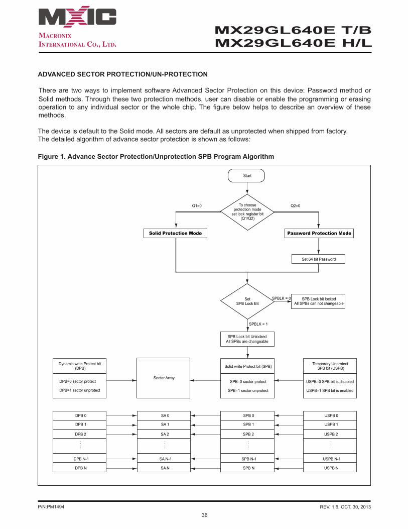
ADVANCED SECTOR PROTECTION/UN-PROTECTION
There are two ways to implement software Advanced Sector Protection on this device: Password method or Solid methods. Through these two protection methods, user can disable or enable the programming or erasing operation to any individual sector or the whole chip. The figure below helps to describe an overview of these methods.
The device is default to the Solid mode. All sectors are default as unprotected when shipped from factory. The detailed algorithm of advance sector protection is shown as follows:
Figure 1. Advance Sector Protection/Unprotection SPB Program Algorithm
Start
Q1=0 Q2=0
Password Protection Mode
To chooseprotection mode
set lock register bit(Q1/Q2)
SPB Lock bit UnlockedAll SPBs are changeable
Solid write Protect bit (SPB)
SPB=0 sector protect
SPB=1 sector unprotect
Temporary Unprotect SPB bit (USPB)
USPB=0 SPB bit is disabled
USPB=1 SPB bit is enabled
USPB 0
USPB 1
USPB 2
::
USPB N-1
USPB N
SPB 0
SPB 1
SPB 2
::
SPB N-1
SPB N
SA 0
SA 1
SA 2
::
SA N-1
SA N
DPB 0
DPB 1
DPB 2
::
DPB N-1
DPB N
SPB Lock bit lockedAll SPBs can not changeable
Solid Protection Mode
Set 64 bit Password
Sector Array
Dynamic write Protect bit (DPB)
DPB=0 sector protect
DPB=1 sector unprotect
SetSPB Lock Bit
SPBLK = 0
SPBLK = 1

37P/N:PM1494 REV. 1.6, OCT. 30, 2013
MX29GL640E T/BMX29GL640E H/L
Figure 2. Lock Register Program Algorithm
START
Pass
Exit Lock Register command
Done YES
YES
NO
Q5 = 1NO
Write Data AAH, Address 555H
Lock register command set EntryWrite Data 55H, Address 2AAH
Write Data 40H, Address 555H
Write Data A0H, Address don’t care
Write Program Data, Address don’t care
Data # Polling Algorithm
Fail
Reset command
Lock register data program
1. Lock Register
User can choose the sector protecting method via setting Lock Register bits as Q1 and Q2. Lock Register is a 16-bit one-time programmable register. Once programming either Q1 or Q2, they will be locked in that mode and the others will be disabled permanently. Q1 and Q2 can not be programmed at the same time, otherwise the device will abort the operation.
If users select Password Protection mode, the password setting is required. Users can set password by issuing password program command.
Lock Register bitsQ15-Q3 Q2 Q1 Q0
Don't care Password Protection Mode Lock Bit
Solid Protection Mode Lock Bit
Secured Silicon Sector Protection Bit
Please refer to the command for Lock Register command set about how to read and program the Lock Register bits.

38P/N:PM1494 REV. 1.6, OCT. 30, 2013
MX29GL640E T/BMX29GL640E H/L
2. Solid Protection Mode
2.1 Solid write Protection Bits (SPB)
The Solid write Protection bits (SPB) are nonvolatile bit with the same endurances as the Flash memory. Each SPB is assigned to each sector individually. The SPB is preprogrammed, and verified prior to erasure are managed by the device, so system monitoring is not necessary.
When SPB is set to “0”, the associated sector may be protected, preventing any program or erase operation on this sector. Whether the sector is protected depends also upon the value of the USPB, as described elsewhere.The SPB bits are set individually by SPB program command. However, it cannot be cleared individually. Issuing the All SPB Erase command will erase all SPB in the same time. During SPB programming period, the read and write operations are disabled for normal sector until exiting this mode.
To unprotect a protected sector, the SPB lock bit must be cleared first by using a hardware reset or a power-up cycle. After the SPB lock bit is cleared, the SPB status can be changed to the desired settings. To lock the Solid Protection Bits after the modification has finished, the SPB Lock Bit must be set once again.
To verify the state of the SPB for a given sector, issuing a SPB Status Read Command to the device is required. Refer to the flow chart for details in Figure 3.
2.2 Dynamic write Protection Bits (DPB)
The Dynamic Protection features a volatile type protection to each individual sector. It can protect sectors from being unintentionally changed, and is easy to disable.
All Dynamic write Protection bit (DPB) can be modified individually. DPBs protect the unprotected sectors with their SPBs cleared. To modify the DPB status by issuing the DPB Set (programmed to “0”) or DPB Clear (erased to “1”) commands, and place each sector in the protected or unprotected state seperately. After the DPB Clear command is issued (erased to “1”), the sector may be modified depending on the SPB state of that sector.
The DPBs are default to be erased to “1” when first shipped from factory.
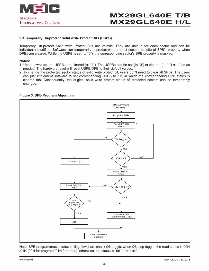
39P/N:PM1494 REV. 1.6, OCT. 30, 2013
MX29GL640E T/BMX29GL640E H/L
Figure 3. SPB Program Algorithm
Q6 Toggle ?
Q6 Toggle ?
Q5 = 1 ?
NO
NO
YES
NO
NO
SPB commandset entry
Program SPB
Read Q7~Q0Twice
Read Q7~Q0Twice
Read Q7~Q0Twice
YES
YES
YES
Wait 500 µs
Program Fail Write Reset CMD
Pass
Q0='1' (Erase)'0' (Program)
SPB commandset Exit
2.3 Temporary Un-protect Solid write Protect Bits (USPB)
Temporary Un-protect Solid write Protect Bits are volatile. They are unique for each sector and can be individually modified. Software can temporarily unprotect write protect sectors despite of SPB's property when DPBs are cleared. While the USPB is set (to “0”), the corresponding sector's SPB property is masked.
Notes:1. Upon power up, the USPBs are cleared (all “1”). The USPBs can be set (to “0”) or cleared (to “1”) as often as
needed. The hardware reset will reset USPB/DPB to their default values.2. To change the protected sector status of solid write protect bit, users don't need to clear all SPBs. The users
can just implement software to set corresponding USPB to "0", in which the corresponding DPB status is cleared too. Consequently, the original solid write protect status of protected sectors can be temporarily changed.
Note: SPB program/erase status polling flowchart: check Q6 toggle, when Q6 stop toggle, the read status is 00H /01H (00H for program/ 01H for erase), otherwise, the status is “fail” and “exit”.

40P/N:PM1494 REV. 1.6, OCT. 30, 2013
MX29GL640E T/BMX29GL640E H/L
4. Password Protection Method
The security level of Password Protection Method is higher than the Solid protection mode. The 64 bit password is requested before modifying SPB lock bit status. When device is under password protection mode, the SPB lock bit is set as “0”, after a power-up cycle or Reset Command.
A correct password is required for password Unlock command to unlock the SPB lock bit. Await 2us is necessary to unlock the device after a valid password is given. After that, the SPB bits are allowed to be changed. The Password Unlock command is issued slower than 2 μs every time, to prevent hacker from trying all the 64-bit password combinations.
There are a few steps to start password protection mode:(1). Set a 64-bit password for verification before entering the password protection mode. This verification is only
allowed in password programming.(2). Set the Password Protection Mode Lock Bit to”0” to activate the password protection mode.
Once the password protection mode lock bit is programmed, the programmed Q2 bit can not be erased any more and the device will remain permanently in password protection mode. The previous set 64-bit password can not be retrieved or programmed. All the commands to the password-protected address will also be disabled.
All the combinations of the 64-bit password can be used as a password, and programming the password does not require special address. The password is defaulted to be all “1” when shipped from the factory. Under password program command, only "0" can be programmed. In order to prevent access, the Password Mode Locking Bit must be set after the Password is programmed and verified. To set the Password Mode Lock Bit will prevent this 64-bits password to be read on the data bus. Any modification is impossible then, and the password can not be checked anymore after the Password Mode Lock Bit is set.
3. Solid Protection Bit Lock Bit
The Solid Protection Bit Lock Bit (SPBLK) is assigned to control all SPB status. It is an unique and volatile. When SPBLK=0 (set), all SPBs are locked and can not be changed. When SPBLK=1 (cleared), all SPBs are allowed to be changed.
There is no software command sequence requested to unlock this bit, unless the device is in the password protection mode. To clear the SPB Lock Bit, just execute a hardware reset or a power-up cycle. In order to prevent modification, the SPB Lock Bit must be set (SPBLK=0) after all SPBs are set to desired status.
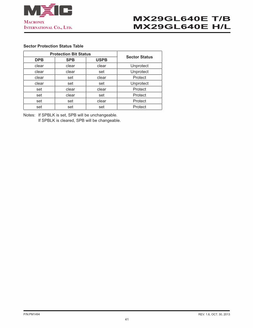
41P/N:PM1494 REV. 1.6, OCT. 30, 2013
MX29GL640E T/BMX29GL640E H/L
Sector Protection Status Table
Protection Bit StatusSector Status
DPB SPB USPBclear clear clear Unprotectclear clear set Unprotectclear set clear Protectclear set set Unprotectset clear clear Protectset clear set Protectset set clear Protectset set set Protect
Notes: If SPBLK is set, SPB will be unchangeable. If SPBLK is cleared, SPB will be changeable.

42P/N:PM1494 REV. 1.6, OCT. 30, 2013
MX29GL640E T/BMX29GL640E H/L
Secured Silicon Sector Address Range Standard Factory Locked Express Flash
Factory Locked Customer Lockable
000000h-000007h ESN ESN or Determined by Customer Determined by Customer
000008h-00007Fh Unavailable Determined by Customer
Customer Lockable: Security Sector NOT Programmed or Protected at the Factory
When the security feature is not required, the security region can act as an extra memory space.
Security silicon sector can also be protected by two methods. Note that once the security silicon sector is pro-tected, there is no way to unprotect the security silicon sector and the content of it can no longer be altered.
After the security silicon is locked and verified, system must write Exit Security Sector Region, go through a pow-er cycle, or issue a hardware reset to return the device to read normal array mode.
SECURITY SECTOR FLASH MEMORY REGION
The Security Sector region is an extra OTP memory space of 128 words in length. The security sector can be locked upon shipping from factory, or it can be locked by customer after shipping. Customer can issue Security Sector Factory Protect Verify and/or Security Sector Protect Verify to query the lock status of the device.
In factory-locked device, security sector region is protected when shipped from factory and the security silicon sector indicator bit, Q7 (at Autoslect address 03h) is set to "1". In customer lockable device, security sector re-gion is unprotected when shipped from factory and the security silicon indicator bit is set to "0".
Factory Locked: Security Sector Programmed and Protected at the Factory
In a factory locked device, the Security Sector is permanently locked before shipping from the factory. The de-vice will have a 16-byte (8-word) ESN in the security region.
Security Sector Address for MX29GL640ET device
Security Sector Address for MX29GL640EB device
Security Sector Address for MX29GL640E H/L device
Secured Silicon Sector Address Range Standard Factory Locked Express Flash
Factory Locked Customer Lockable
3FFF80h-3FFF87h ESN ESN or Determined by Customer Determined by Customer
3FFF88h-3FFFFFh Unavailable Determined by Customer
Secured Silicon Sector Address Range Standard Factory Locked Express Flash
Factory Locked Customer Lockable
000000h-000007h ESN ESN or Determined by Customer Determined by Customer
000008h-00007Fh Unavailable Determined by Customer

43P/N:PM1494 REV. 1.6, OCT. 30, 2013
MX29GL640E T/BMX29GL640E H/L
TABLE 3. COMMAND DEFINITIONS
WA= Write AddressWD= Write DataSA= Sector AddressN= Word CountWBL= Write Buffer LocationPWD= PasswordPWDn=Password word 0, word 1, word nID1/ID2/ID3: Refer to Table 2-2 for detail ID of each device.
Comm-and
Read Mode
Reset Mode
Automatic Select Security Sector Region
Exit Security SectorSilicon ID Device ID Factory Protect
Verify Sector Protect Verify
Word Byte Word Byte Word Byte Word Byte Word Byte Word Byte1st Bus Cycle
Addr Addr XXX 555 AAA 555 AAA 555 AAA 555 AAA 555 AAA 555 AAAData Data F0 AA AA AA AA AA AA AA AA AA AA AA AA
2nd Bus Cycle
Addr 2AA 555 2AA 555 2AA 555 2AA 555 2AA 555 2AA 555Data 55 55 55 55 55 55 55 55 55 55 55 55
3rd Bus Cycle
Addr 555 AAA 555 AAA 555 AAA 555 AAA 555 AAA 555 AAAData 90 90 90 90 90 90 90 90 88 88 90 90
4th Bus Cycle
Addr X00 X00 X01 X02 X03 X06 (Sector)X02
(Sector)X04 XXX XXX
Data C2h C2h ID1 ID1 9A/1A(H) 8A/0A(L) 00/01 00/01 00 00
5th Bus Cycle
Addr X0E X1CData ID2 ID2
6th Bus Cycle
Addr X0F X1EData ID3 ID3
Comm-and
ProgramWrite to Buffer
Program
Write to Buffer
Program Abort Reset
Write to Buffer
Program confirm
Chip Erase Sector Erase CFI Read
Program/Erase
Suspend
Program/Erase
Resume
Word Byte Word Byte Word Byte Word Byte Word Byte Word Byte Word Byte Word Byte Word Byte
1st Bus Cycle
Addr 555 AAA 555 AAA 555 AAA SA SA 555 AAA 555 AAA 55 AA xxx xxx xxx xxxData AA AA AA AA AA AA 29 29 AA AA AA AA 98 98 B0 B0 30 30
2nd Bus Cycle
Addr 2AA 555 2AA 555 2AA 555 2AA 555 2AA 555Data 55 55 55 55 55 55 55 55 55 55
3rd Bus Cycle
Addr 555 AAA SA SA 555 AAA 555 AAA 555 AAAData A0 A0 25 25 F0 F0 80 80 80 80
4th Bus Cycle
Addr Addr Addr SA SA 555 AAA 555 AAAData Data Data N-1 N-1 AA AA AA AA
5th Bus Cycle
Addr WA WA 2AA 555 2AA 555Data WD WD 55 55 55 55
6th Bus Cycle
Addr WBL WBL 555 AAA Sec-tor
Sec-tor
Data WD WD 10 10 30 30

44P/N:PM1494 REV. 1.6, OCT. 30, 2013
MX29GL640E T/BMX29GL640E H/L
Command
Deep Power Down Password Protection
Enter ExitPassword
Command Set Entry
Password Program
Password Read
Password Unlock
Password Command Set
ExitWord Byte Word Byte Word Byte Word Byte Word Byte Word Byte Word Byte
1st Bus Cycle
Addr 555 AAA XXX XXX 555 AAA XXX XXX X00 X00 00 00 XXX XXXData AA AA AB AB AA AA A0 A0 PWD0 PWD0 25 25 90 90
2nd Bus Cycle
Addr 2AA 555 2AA 555 PWA PWA X01 X01 00 00 XXX XXXData 55 55 55 55 PWD PWD PWD1 PWD1 03 03 00 00
3rd Bus Cycle
Addr XXX XXX 555 AAA X02 X02 X00 X00Data B9 B9 60 60 PWD2 PWD2 PWD0 PWD0
4th Bus Cycle
Addr X03 X03 X01 X01Data PWD3 PWD3 PWD1 PWD1
5th Bus Cycle
Addr X04 X02 X02Data PWD4 PWD2 PWD2
6th Bus Cycle
Addr X05 X03 X03Data PWD5 PWD3 PWD3
7th Bus Cycle
Addr X06 00 X04Data PWD6 29 PWD4
8th Bus Cycle
Addr X07 X05Data PWD7 PWD5
9th Bus Cycle
Addr X06Data PWD6
10th Bus Cycle
Addr X07Data PWD7
11th Bus Cycle
Addr 00Data 29
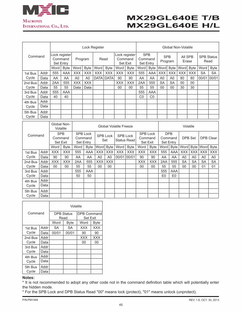
45P/N:PM1494 REV. 1.6, OCT. 30, 2013
MX29GL640E T/BMX29GL640E H/L
Command
Lock Register Global Non-Volatile
Lock register Command Set Entry
Program ReadLock register Command
Set Exit
SPB Command Set Entry
SPB Program
All SPB Erase
SPB Status Read
Word Byte Word Byte Word Byte Word Byte Word Byte Word Byte Word Byte Word Byte1st Bus Cycle
Addr 555 AAA XXX XXX XXX XXX XXX XXX 555 AAA XXX XXX XXX XXX SA SAData AA AA A0 A0 DATA DATA 90 90 AA AA A0 A0 80 80 00/01 00/01
2nd Bus Cycle
Addr 2AA 555 XXX XXX XXX XXX 2AA 555 SA SA 00 00Data 55 55 Data Data 00 00 55 55 00 00 30 30
3rd Bus Cycle
Addr 555 AAA 555 AAA Data 40 40 C0 C0
4th Bus Cycle
AddrData
5th Bus Cycle
AddrData
Command
Global Non-Volatile Global Volatile Freeze Volatile
SPB Command
Set Exit
SPB Lock Command Set Entry
SPB Lock Set
SPB Lock Status Read
SPB Lock Command
Set Exit
DPB Command Set Entry
DPB Set DPB Clear
Word Byte Word Byte Word Byte Word Byte Word Byte Word Byte Word Byte Word Byte1st Bus Cycle
Addr XXX XXX 555 AAA XXX XXX XXX XXX XXX XXX 555 AAA XXX XXX XXX XXXData 90 90 AA AA A0 A0 00/01 00/01 90 90 AA AA A0 A0 A0 A0
2nd Bus Cycle
Addr XXX XXX 2AA 555 XXX XXX XXX XXX 2AA 555 SA SA SA SAData 00 00 55 55 00 00 00 00 55 55 00 00 01 01
3rd Bus Cycle
Addr 555 AAA 555 AAA Data 50 50 E0 E0
4th Bus Cycle
AddrData
5th Bus Cycle
AddrData
Command
Volatile
DPB Status Read
DPB Command Set Exit
Word Byte Word Byte1st Bus Cycle
Addr SA SA XXX XXXData 00/01 00/01 90 90
2nd Bus Cycle
Addr XXX XXXData 00 00
3rd Bus Cycle
AddrData
4th Bus Cycle
AddrData
5th Bus Cycle
AddrData
Notes: * It is not recommended to adopt any other code not in the command definition table which will potentially enter the hidden mode.* For the SPB Lock and DPB Status Read "00" means lock (protect), "01" means unlock (unprotect).

46P/N:PM1494 REV. 1.6, OCT. 30, 2013
MX29GL640E T/BMX29GL640E H/L
Table 4-2. CFI mode: System Interface Data Values
COMMON FLASH MEMORY INTERFACE (CFI) MODE
QUERY COMMAND AND COMMAND FLASH MEMORY INTERFACE (CFI) MODE
The device features CFI mode. Host system can retrieve the operating characteristics, structure and vendor-specified information such as identifying information, memory size, byte/word configuration, operating voltages and timing information of this device by CFI mode. If the system writes the CFI Query command "98h", to ad-dress "55h"/"AAh" (depending on Word/Byte mode), the device will enter the CFI Query Mode, any time the de-vice is ready to read array data. The system can read CFI information at the addresses given in Table 4.
Once user enters CFI query mode, user can issue reset command to exit CFI mode and return to read array mode. The unused CFI area is reserved by Macronix.
DescriptionAddress (h) (Word Mode)
Address (h)(Byte Mode)
Data (h)
Vcc supply minimum program/erase voltage 1B 36 0027Vcc supply maximum program/erase voltage 1C 38 0036VPP supply minimum program/erase voltage 1D 3A 0000VPP supply maximum program/erase voltage 1E 3C 0000Typical timeout per single word/byte write, 2n us 1F 3E 0003Typical timeout for maximum-size buffer write, 2n us (00h, not support)
20 40 0006
Typical timeout per individual block erase, 2n ms 21 42 0009Typical timeout for full chip erase, 2n ms (00h, not support) 22 44 0013Maximum timeout for word/byte write, 2n times typical 23 46 0003Maximum timeout for buffer write, 2n times typical 24 48 0005Maximum timeout per individual block erase, 2n times typical 25 4A 0003Maximum timeout for chip erase, 2n times typical (00h, not support)
26 4C 0002
DescriptionAddress (h) (Word Mode)
Address (h)(Byte Mode)
Data (h)
Query-unique ASCII string "QRY"10 20 005111 22 005212 24 0059
Primary vendor command set and control interface ID code 13 26 000214 28 0000
Address for primary algorithm extended query table 15 2A 004016 2C 0000
Alternate vendor command set and control interface ID code 17 2E 000018 30 0000
Address for alternate algorithm extended query table 19 32 00001A 34 0000
Table 4-1. CFI mode: Identification Data Values (Note 1) (All values in these tables are in hexadecimal)
Note 1. Query data are always presented on the lowest data output Q7~Q0 only, Q8~Q15 are "0".

47P/N:PM1494 REV. 1.6, OCT. 30, 2013
MX29GL640E T/BMX29GL640E H/L
Table 4-3. CFI mode: Device Geometry Data Values
DescriptionAddress (h) (Word Mode)
Address (h)(Byte Mode)
Data (h)
Device size = 2n in number of bytes (17=64Mb) 27 4E 0017
Flash device interface description (02=asynchronous x8/x16)28 50 000229 52 0000
Maximum number of bytes in buffer write = 2n (00h, not support)2A 54 00052B 56 0000
Number of erase regions within device29GL640E T/B=02 (boot device)29GL640E H/L=01 (uniform device)
2C 58 00XX
Index for Erase Bank Area 1:[2E,2D] = # of same-size sectors in region 1-1[30, 2F] = sector size in multiples of 256-bytes29GL640E T/B=0007, 0000, 0020, 000029GL640E H/L=007F, 0000, 0000, 0001
2D 5A 00XX2E 5C 0000
2F 5E 00XX
30 60 00XX
Index for Erase Bank Area 229GL640E T/B=007E, 0000, 0000, 000129GL640E H/L=0000, 0000, 0000, 0000
31 62 00XX32 64 000033 66 000034 68 00XX
Index for Erase Bank Area 3
35 6A 000036 6C 000037 6E 000038 70 0000
Index for Erase Bank Area 4
39 72 00003A 74 00003B 76 00003C 78 0000

48P/N:PM1494 REV. 1.6, OCT. 30, 2013
MX29GL640E T/BMX29GL640E H/L
Table 4-4. CFI mode: Primary Vendor-Specific Extended Query Data Values
DescriptionAddress (h) (Word Mode)
Address (h)(Byte Mode)
Data (h)
Query - Primary extended table, unique ASCII string, PRI40 80 005041 82 005242 84 0049
Major version number, ASCII 43 86 0031Minor version number, ASCII 44 88 0033Unlock recognizes address (Bits 1-0)0= recognize, 1= don't recognize Process Technology (Bits 7-2) 0101b=110nm
45 8A 0014
Erase suspend (2= to both read and program) 46 8C 0002Sector protect (N= # of sectors/group) 47 8E 0001Temporary sector unprotect (1=supported) 48 90 0000Sector protect/Chip unprotect scheme 49 92 0008Simultaneous R/W operation (0=not supported) 4A 94 0000Burst mode (0=not supported) 4B 96 0000Page mode (0=not supported, 01 = 4 word page, 02 = 8 word page) 4C 98 0002
Minimum ACC(acceleration) supply (0= not supported), [D7:D4] for volt, [D3:D0] for 100mV 4D 9A 0095
Maximum ACC(acceleration) supply (0= not supported), [D7:D4] for volt, [D3:D0] for 100mV 4E 9C 00A5
WP# Protection Flag29GL640EB=02 (Bottom Boot Sectors WP# Protect)29GL640ET=03 (Top Boot Sectors WP# Protect)29GL640EL=04 (Uniform Sectors Bottom WP# Protect)29GL640EH=05 (Uniform Sectors Top WP# Protect)
4F 9E 00XX
Program Suspend (0=not supported, 1=supported) 50 A0 0001
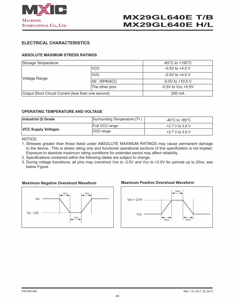
49P/N:PM1494 REV. 1.6, OCT. 30, 2013
MX29GL640E T/BMX29GL640E H/L
ABSOLUTE MAXIMUM STRESS RATINGS
OPERATING TEMPERATURE AND VOLTAGE
ELECTRICAL CHARACTERISTICS
Storage Temperature -65°C to +150°C
Voltage Range
VCC -0.5V to +4.0 V
VI/O -0.5V to +4.0 V
A9 , WP#/ACC -0.5V to +10.5 VThe other pins. -0.5V to Vcc +0.5V
Output Short Circuit Current (less than one second) 200 mA
Industrial (I) Grade Surrounding Temperature (TA ) -40°C to +85°C
VCC Supply VoltagesFull VCC range +2.7 V to 3.6 VVI/O range +2.7 V to 3.6 V
NOTICE:1. Stresses greater than those listed under ABSOLUTE MAXIMUM RATINGS may cause permanent damage
to the device. This is stress rating only and functional operational sections of this specification is not implied. Exposure to absolute maximum rating conditions for extended period may affect reliability.
2. Specifications contained within the following tables are subject to change.3. During voltage transitions, all pins may overshoot Vss to -2.0V and Vcc to +2.0V for periods up to 20ns, see
below Figure.
Maximum Negative Overshoot Waveform Maximum Positive Overshoot Waveform
Vss
Vss - 2.0V
20ns 20ns
20ns
Vcc + 2.0V
Vcc
20ns 20ns
20ns
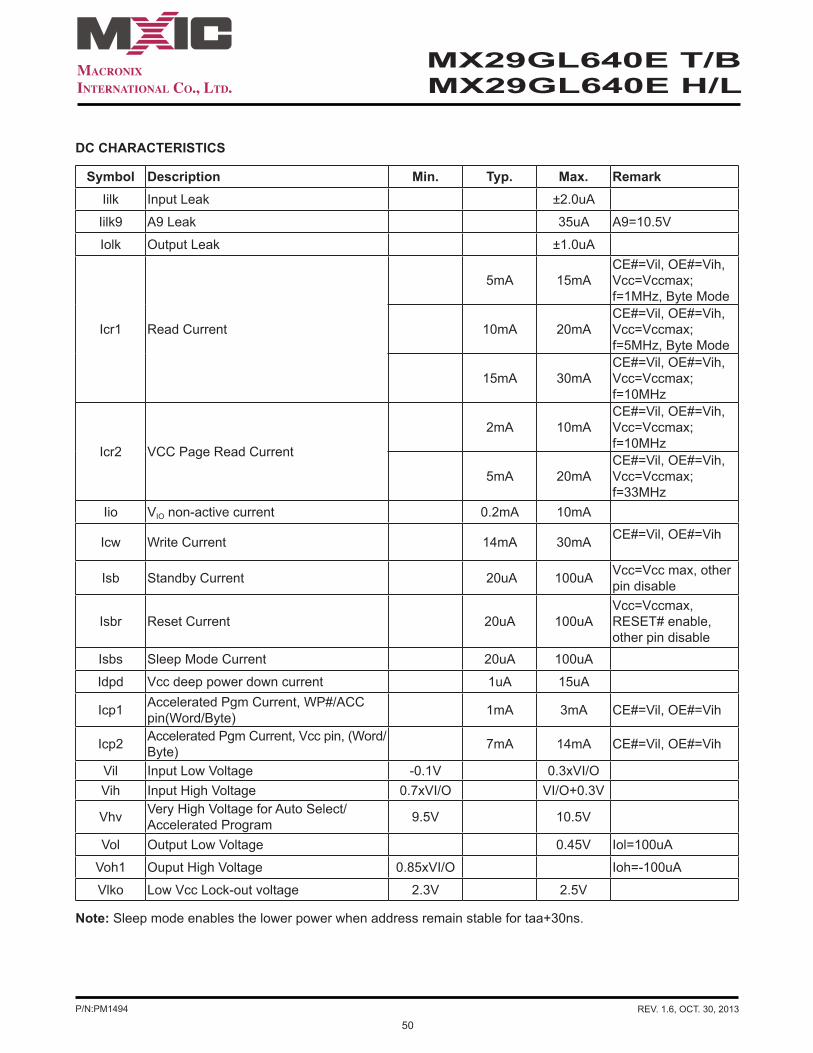
50P/N:PM1494 REV. 1.6, OCT. 30, 2013
MX29GL640E T/BMX29GL640E H/L
DC CHARACTERISTICS
Symbol Description Min. Typ. Max. RemarkIilk Input Leak ±2.0uA
Iilk9 A9 Leak 35uA A9=10.5V
Iolk Output Leak ±1.0uA
Icr1 Read Current
5mA 15mACE#=Vil, OE#=Vih, Vcc=Vccmax; f=1MHz, Byte Mode
10mA 20mACE#=Vil, OE#=Vih, Vcc=Vccmax; f=5MHz, Byte Mode
15mA 30mACE#=Vil, OE#=Vih, Vcc=Vccmax; f=10MHz
Icr2 VCC Page Read Current
2mA 10mACE#=Vil, OE#=Vih, Vcc=Vccmax; f=10MHz
5mA 20mACE#=Vil, OE#=Vih, Vcc=Vccmax; f=33MHz
Iio VIO non-active current 0.2mA 10mA
Icw Write Current 14mA 30mA CE#=Vil, OE#=Vih
Isb Standby Current 20uA 100uA Vcc=Vcc max, other pin disable
Isbr Reset Current 20uA 100uAVcc=Vccmax, RESET# enable, other pin disable
Isbs Sleep Mode Current 20uA 100uA
Idpd Vcc deep power down current 1uA 15uA
Icp1 Accelerated Pgm Current, WP#/ACC pin(Word/Byte) 1mA 3mA CE#=Vil, OE#=Vih
Icp2 Accelerated Pgm Current, Vcc pin, (Word/Byte) 7mA 14mA CE#=Vil, OE#=Vih
Vil Input Low Voltage -0.1V 0.3xVI/OVih Input High Voltage 0.7xVI/O VI/O+0.3V
Vhv Very High Voltage for Auto Select/Accelerated Program 9.5V 10.5V
Vol Output Low Voltage 0.45V Iol=100uA
Voh1 Ouput High Voltage 0.85xVI/O Ioh=-100uA
Vlko Low Vcc Lock-out voltage 2.3V 2.5V
Note: Sleep mode enables the lower power when address remain stable for taa+30ns.

51P/N:PM1494 REV. 1.6, OCT. 30, 2013
MX29GL640E T/BMX29GL640E H/L
SWITCHING TEST CIRCUITS
SWITCHING TEST WAVEFORMS
Test Condition Output Load Capacitance, CL : 1TTL gate, 30pFRise/Fall Times : 5nsInput Pulse levels :0.0 ~ VI/OIn/Out reference levels :0.5VI/O
Test Points
VI/O
VI/O / 2VI/O / 2
0.0VOUTPUTINPUT
DEVICE UNDERTEST
CL
3.3V
6.2KΩ
2.7KΩ

52P/N:PM1494 REV. 1.6, OCT. 30, 2013
MX29GL640E T/BMX29GL640E H/L
AC CHARACTERISTICS
Symbol Description29GL640E
(VCC=2.7V~3.6V) UnitMin. Typ. Max.
Taa Valid data output after address 70 nsTpa Page access time 25 nsTce Valid data output after CE# low 70 nsToe Valid data output after OE# low 25 nsTdf Data output floating after OE# high 20 ns
Tsrw Latency between read and write operation (Note) 35 ns
Toh Output hold time from the earliest rising edge of address,CE#, OE# 0 ns
Trc Read period time 70 nsTwc Write period time 70 nsTcwc Command write period time 70 nsTas Address setup time 0 nsTah Address hold time 45 nsTds Data setup time 30 nsTdh Data hold time 0 nsTvcs Vcc setup time 500 usTcs Chip enable Setup time 0 nsTch Chip enable hold time 0 ns
Toes Output enable setup time 0 ns
Toeh Output enable hold time Read 0 nsToggle & Data# Polling 10 ns
Tws WE# setup time 0 nsTwh WE# hold time 0 ns
Tcepw CE# pulse width 35 nsTcepwh CE# pulse width high 30 ns
Twp WE# pulse width 35 nsTwph WE# pulse width high 30 nsTbusy Program/Erase active time by RY/BY# 70 nsTghwl Read recover time before write 0 nsTghel Read recover time before write 0 ns
Twhwh1 Program operationByte 10 usWord 10 us
Twhwh1 Acc program operation (Word/Byte) 10 usTwhwh2 Sector erase operation 0.5 3.5 sec
Tbal Sector add hold time 50 usTrdp Release from deep power down mode 200 us
Note : Not 100% tested.

53P/N:PM1494 REV. 1.6, OCT. 30, 2013
MX29GL640E T/BMX29GL640E H/L
Figure 4. COMMAND WRITE OPERATION
Addresses
CE#
OE#
WE#
DIN
Tds
Tah
Data
Tdh
Tcs Tch
Tcwc
TwphTwpToes
Tas
Vih
Vil
Vih
Vil
Vih
Vil
Vih
Vil
Vih
Vil
VA
VA: Valid Address

54P/N:PM1494 REV. 1.6, OCT. 30, 2013
MX29GL640E T/BMX29GL640E H/L
READ/RESET OPERATION
Figure 5. READ TIMING WAVEFORMS
Addresses
CE#
OE#
Taa
WE#
Vih
Vil
Vih
Vil
Vih
Vil
Vih
Vil
Voh
Vol
HIGH Z HIGH ZDATA Valid
ToeToeh Tdf
Tce
Trc
Outputs
Toh
ADD Valid

55P/N:PM1494 REV. 1.6, OCT. 30, 2013
MX29GL640E T/BMX29GL640E H/L
Figure 6. RESET# TIMING WAVEFORM
Trh
Trb1
Trp2
Trp1
Tready2
Tready1
RY/BY#
CE#, OE#
RESET#
Reset Timing NOT during Automatic Algorithms
Reset Timing during Automatic Algorithms
RY/BY#
CE#, OE#
Trb2
WE#
RESET#
AC CHARACTERISTICS
Item Description Setup Speed UnitTrp1 RESET# Pulse Width (During Automatic Algorithms) MIN 10 us
Trp2 RESET# Pulse Width (NOT During Automatic Algorithms) MIN 500 ns
Trh RESET# High Time Before Read MIN 200 ns
Trb1 RY/BY# Recovery Time (to CE#, OE# go low) MIN 0 ns
Trb2 RY/BY# Recovery Time (to WE# go low) MIN 50 ns
Tready1 RESET# PIN Low (During Automatic Algorithms) to Read or Write MAX 20 us
Tready2 RESET# PIN Low (NOT During Automatic Algorithms) to Read or Write MAX 500 ns

56P/N:PM1494 REV. 1.6, OCT. 30, 2013
MX29GL640E T/BMX29GL640E H/L
ERASE/PROGRAM OPERATION
Figure 7. AUTOMATIC CHIP ERASE TIMING WAVEFORM
Twc
Address
OE#
CE#
55h
2AAh 555h
10h
InProgress Complete
VA VA
Tas Tah
Tghwl
Tch
Twp
Tds Tdh
Twhwh2
Read StatusLast 2 Erase Command Cycle
Tbusy Trb
Tcs TwphWE#
Data
RY/BY#

57P/N:PM1494 REV. 1.6, OCT. 30, 2013
MX29GL640E T/BMX29GL640E H/L
Figure 8. AUTOMATIC CHIP ERASE ALGORITHM FLOWCHART
START
Write Data AAH Address 555H
Write Data 55H Address 2AAH
Write Data AAH Address 555H
Write Data 80H Address 555H
YES
NOData=FFh ?
Write Data 10H Address 555H
Write Data 55H Address 2AAH
Data# Polling Algorithm or
Toggle Bit Algorithm
Auto Chip Erase Completed

58P/N:PM1494 REV. 1.6, OCT. 30, 2013
MX29GL640E T/BMX29GL640E H/L
Figure 9. AUTOMATIC SECTOR ERASE TIMING WAVEFORM
Twc
Address
OE#
CE#
55h
2AAh SectorAddress 1
SectorAddress 0
30h
InProgress Complete
VA VA
30h
SectorAddress n
Tas
Tah
Tbal
Tghwl
Tch
Twp
Tds Tdh
Twhwh2
Read Status
Last 2 Erase Command Cycle
TbusyTrb
Tcs TwphWE#
Data
RY/BY#
30h

59P/N:PM1494 REV. 1.6, OCT. 30, 2013
MX29GL640E T/BMX29GL640E H/L
Figure 10. AUTOMATIC SECTOR ERASE ALGORITHM FLOWCHART
START
Write Data AAH Address 555H
Write Data 55H Address 2AAH
Write Data AAH Address 555H
Write Data 80H Address 555H
Write Data 30H Sector Address
Write Data 55H Address 2AAH
Data# Polling Algorithm or
Toggle Bit Algorithm
Auto Sector Erase Completed
NOLast Sector
to Erase
YES
YES
NOData=FFh
60P/N:PM1494 REV. 1.6, OCT. 30, 2013
MX29GL640E T/BMX29GL640E H/L
Figure 11. ERASE SUSPEND/RESUME FLOWCHART
START
Write Data B0H
Toggle Bit checking Q6 not toggled
ERASE SUSPEND
YES
NO
Write Data 30H
Continue Erase
Reading or Programming End
Read Array orProgram
AnotherErase Suspend ?
NO
YES
YES
NO
ERASE RESUME

61P/N:PM1494 REV. 1.6, OCT. 30, 2013
MX29GL640E T/BMX29GL640E H/L
Figure 12. AUTOMATIC PROGRAM TIMING WAVEFORMS
Figure 13. ACCELERATED PROGRAM TIMING DIAGRAM
Address
OE#
CE#
A0h
555h PA
PD Status DOUT
VA VA
Tas Tah
Tghwl
Tch
Twp
Tds Tdh
Twhwh1
Last 2 Read Status CycleLast 2 Program Command Cycle
TbusyTrb
Tcs TwphWE#
Data
RY/BY#
WP#/ACC
Vcc
250ns 250ns
Vhv (9.5V ~ 10.5V)
Vil or Vih Vil or Vih
Tvcs
Vcc (min)
GND

62P/N:PM1494 REV. 1.6, OCT. 30, 2013
MX29GL640E T/BMX29GL640E H/L
Figure 14. CE# CONTROLLED WRITE TIMING WAVEFORM
Address
OE#
CE#
A0h
555h PA
PD Status DOUT
VA VA
Tas Tah
Tghwl
TcepwTws Twh
Tds Tdh
Twhwh1 or Twhwh2
Tbusy
Tcepwh
WE#
Data
RY/BY#

63P/N:PM1494 REV. 1.6, OCT. 30, 2013
MX29GL640E T/BMX29GL640E H/L
Figure 15. AUTOMATIC PROGRAMMING ALGORITHM FLOWCHART
START
Write Data AAH Address 555H
Write Data 55H Address 2AAH
Write Program Data/Address
Write Data A0H Address 555H
YES
Read Again Data:Program Data?
YES
Auto Program Completed
Data# Polling Algorithm orToggle Bit Algorithm
next address
Last Word to beProgramed
No
No

64P/N:PM1494 REV. 1.6, OCT. 30, 2013
MX29GL640E T/BMX29GL640E H/L
Figure 16. SILICON ID READ TIMING WAVEFORM
Taa Taa Taa Taa
Tce
Toe
Toh Toh Toh Toh
Tdf
DATA OUT
Manufacturer ID Device IDCycle 1
Device IDCycle 2
Device IDCycle 3
VhvVihVil
ADDA9
ADD
CE#
A1
OE#
WE#
ADDA0
DATA OUT DATA OUT DATA OUTDATAQ15~Q0
VCC3V
Vih
Vil
Vih
Vil
Vih
Vil
Vih
Vil
Vih
Vil
Vih
Vil
Vih
Vil
A2
Disable
Enable

65P/N:PM1494 REV. 1.6, OCT. 30, 2013
MX29GL640E T/BMX29GL640E H/L
WRITE OPERATION STATUS
Figure 17. DATA# POLLING TIMING WAVEFORMS (DURING AUTOMATIC ALGORITHMS)
Tdf
Tce
Tch
Toe
Toeh
Toh
CE#
OE#
WE#
Q7
Q6~Q0
RY/BY#
Tbusy
Status Data Status Data
ComplementComplement True Valid Data
Taa
Trc
Address VAVA
High Z
High ZValid DataTrue

66P/N:PM1494 REV. 1.6, OCT. 30, 2013
MX29GL640E T/BMX29GL640E H/L
Figure 18. STATUS POLLING FOR WORD PROGRAM/ERASE
Notes:1. For programming, valid address means program address. For erasing, valid address means erase sectors address.2. Q7 may change simultaneously with Q5, so even Q5=1, Q7 should be reverify.
Start
Q7 = Data# ?
Q5 = 1 ?
Q7 = Data# ?(Note 2)
FailPass
No
No
No
Yes
Yes
Yes
Read Data at valid address(Note 1)
Read Data at valid address(Note 1)

67P/N:PM1494 REV. 1.6, OCT. 30, 2013
MX29GL640E T/BMX29GL640E H/L
Figure 19. STATUS POLLING FOR WRITE BUFFER PROGRAM
Read Data at last writeaddress (Note 1)
Start
Q7 = Data# ?
Q1=1 ?Only for write
buffer program
Q7 = Data# ?(Note 2)
Fail Pass
Write Buffer Abort
No
No
No
No
No
Yes
Yes
Q5=1 ?
Yes
Yes
Yes
Read Data at last writeaddress (Note 1)
Q7 = Data# ?(Note 2)
Read Data at last writeaddress (Note 1)
Notes:1. For programming, valid address means program address. For erasing, valid address means erase sectors address.2. Q7 may change simultaneously with Q5, so even Q5=1, Q7 should be reverify.
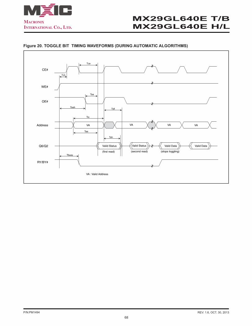
68P/N:PM1494 REV. 1.6, OCT. 30, 2013
MX29GL640E T/BMX29GL640E H/L
Figure 20. TOGGLE BIT TIMING WAVEFORMS (DURING AUTOMATIC ALGORITHMS)
Tdf
Tce
Tch
Toe
Toeh
Taa
Trc
Toh
Address
CE#
OE#
WE#
Q6/Q2
RY/BY#
Tbusy
Valid Status
(first read)
Valid Status
(second read) (stops toggling)
Valid Data
VA VAVA
VA : Valid Address
VA
Valid Data
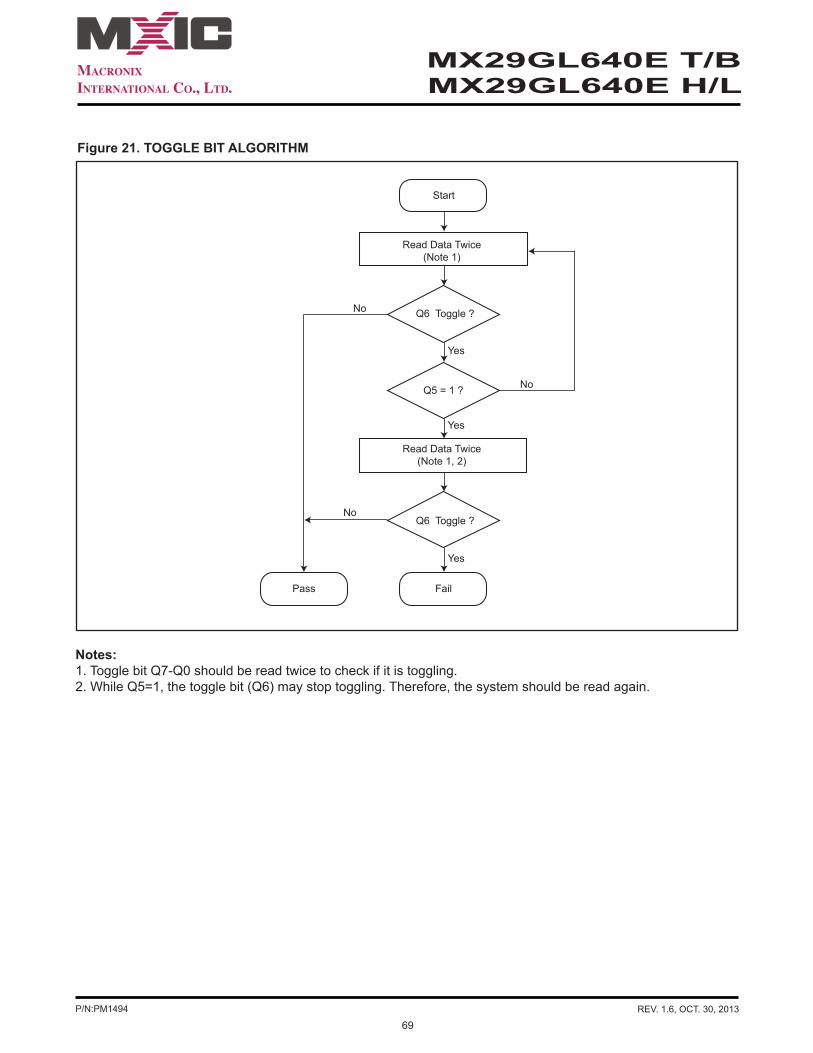
69P/N:PM1494 REV. 1.6, OCT. 30, 2013
MX29GL640E T/BMX29GL640E H/L
Figure 21. TOGGLE BIT ALGORITHM
Notes:1. Toggle bit Q7-Q0 should be read twice to check if it is toggling.2. While Q5=1, the toggle bit (Q6) may stop toggling. Therefore, the system should be read again.
Start
Q5 = 1 ?
FailPass
No
No
No
Yes
Yes
Yes
Read Data Twice(Note 1)
Read Data Twice(Note 1, 2)
Q6 Toggle ?
Q6 Toggle ?

70P/N:PM1494 REV. 1.6, OCT. 30, 2013
MX29GL640E T/BMX29GL640E H/L
Figure 22. BYTE# TIMING WAVEFORM FOR READ OPERATIONS (BYTE# switching from byte mode to word mode)
AC CHARACTERISTICS
WORD/BYTE CONFIGURATION (BYTE#)
Parameter Description Test Setup All Speed Options Unit
Telfl/Telfh CE# to BYTE# from L/H Max. 5 nsTflqz BYTE# from L to Output Hiz Max. 30 nsTfhqv BYTE# from H to Output Active Min. 70 ns
Figure 23. PAGE READ TIMING WAVEFORM
Tfhqv
Telfh
DOUT(Q0-Q7)
DOUT(Q0-Q14)
VA DOUT(Q15)
CE#
OE#
BYTE#
Q14~Q0
Q15/A-1
Amax:A3
(A-1),A0,A1,A2
DATA
CE#
Note: CE#, OE# are enable. Page size is 8 words in Word mode, 16 bytes in Byte mode. Address are A2~A0 for Word mode, A2~A-1 for Byte mode.
VALID ADD
Data 1 Data 2 Data 3
1'st ADD 2'nd ADD
Tpa Taa
3'rd ADD
Tpa
OE#
Tce
Toe

71P/N:PM1494 REV. 1.6, OCT. 30, 2013
MX29GL640E T/BMX29GL640E H/L
Figure 24. DEEP POWER DOWN MODE WAVEFORM
CEB
WEB
ADD
DATA
XX
B9
2AA55
tDP
XX (don't care)
AB
Standby mode
AA 55
Deep power down mode
tRDP
Standby mode
ITEM TYP. MAX.WEB high to release from deep power down mode tRDP 100us 200us
WEB high to deep power down mode tDP 10us 20us
AC CHARACTERISTICS
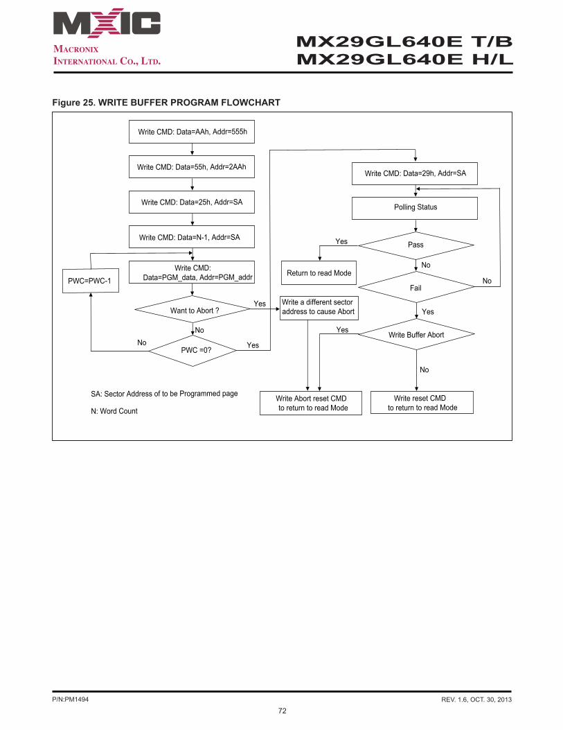
72P/N:PM1494 REV. 1.6, OCT. 30, 2013
MX29GL640E T/BMX29GL640E H/L
Figure 25. WRITE BUFFER PROGRAM FLOWCHART
Write CMD: Data=AAh, Addr=555h
Write CMD: Data=55h, Addr=2AAh
Write CMD: Data=25h, Addr=SA
SA: Sector Address of to be Programmed page
Write CMD: Data=N-1, Addr=SA
N: Word Count
Write CMD:Data=PGM_data, Addr=PGM_addr
PWC =0?
Write CMD: Data=29h, Addr=SA
Polling Status
Yes
Pass
No
No
Write Buffer Abort
Write reset CMD to return to read Mode
PWC=PWC-1 NoFail
YesWant to Abort ?
Yes
NoNo
Yes
Return to read Mode
Write Abort reset CMD to return to read Mode
Write a different sector address to cause Abort
Yes
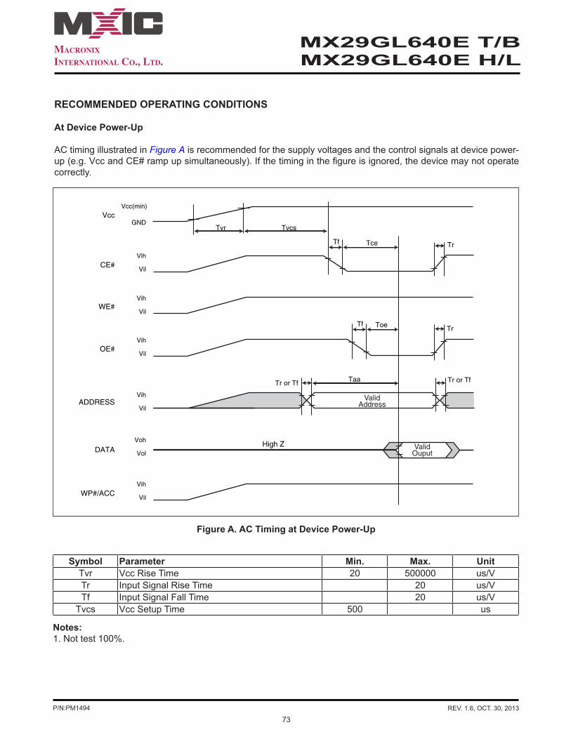
73P/N:PM1494 REV. 1.6, OCT. 30, 2013
MX29GL640E T/BMX29GL640E H/L
RECOMMENDED OPERATING CONDITIONS
At Device Power-Up
AC timing illustrated in Figure A is recommended for the supply voltages and the control signals at device power-up (e.g. Vcc and CE# ramp up simultaneously). If the timing in the figure is ignored, the device may not operate correctly.
Figure A. AC Timing at Device Power-Up
Vcc
ADDRESS
CE#
WE#
OE#
DATA
Tvr
TaaTr or Tf Tr or Tf
TceTf
Vcc(min)
GND
Vih
Vil
Vih
Vil
Vih
Vil
Vih
Vil
Vih
Vil
VohHigh Z
Vol
WP#/ACC
ValidOuput
ValidAddress
Tvcs
Tr
ToeTfTr
Symbol Parameter Min. Max. UnitTvr Vcc Rise Time 20 500000 us/VTr Input Signal Rise Time 20 us/VTf Input Signal Fall Time 20 us/V
Tvcs Vcc Setup Time 500 us
Notes:1. Not test 100%.

74P/N:PM1494 REV. 1.6, OCT. 30, 2013
MX29GL640E T/BMX29GL640E H/L
LATCH-UP CHARACTERISTICS
ERASE AND PROGRAMMING PERFORMANCE
PIN CAPACITANCE
Notes:1. Typical program and erase times assume the following conditions: 25°C, 3.0V VCC. Programming specifica-
tions assume checkboard data pattern.2. Maximum values are measured at VCC = 3.0 V, worst case temperature. Maximum values are valid up to and
including 100,000 program/erase cycles.3. Erase/Program cycles comply with JEDEC JESD-47 & JESD 22-A117 standard.4. Exclude 00h program before erase operation.
Parameter Symbol Parameter Description Test Set Typ. Max. UnitCIN2 Control Pin Capacitance VIN=0 7.5 9 pFCOUT Output Capacitance VOUT=0 8.5 12 pFCIN Input Capacitance VIN=0 6 7.5 pF
Min. Max.Input Voltage voltage difference with GND on WP#/ACC and A9 pins -1.0V 10.5VInput Voltage voltage difference with GND on all normal pins input -1.0V 1.5VccVcc Current -100mA +100mAAll pins included except Vcc. Test conditions: Vcc = 3.0V, one pin per testing
Parameter Limits UnitsMin. Typ. (1) Max. (2)Chip Erase Time 60 150 sec
Sector Erase Time 0.5 3.5 sec
Chip Programming Time (Page Mode) 20 sec
Word Program Time 10 180 us
Total Write Buffer Time 80 400 us
ACC Total Write Buffer Time 75 us
Erase/Program Cycles 100,000 Cycles
DATA RETENTION
Parameter Condition Min. Max. UnitData retention 55˚C 20 years

75P/N:PM1494 REV. 1.6, OCT. 30, 2013
MX29GL640E T/BMX29GL640E H/L
ORDERING INFORMATION
PART NO. ACCESS TIME (ns) PACKAGE RemarkMX29GL640ETTI-70G 70ns 48 Pin TSOP
MX29GL640EBTI-70G 70ns 48 Pin TSOP
MX29GL640ETXEI-70G 70ns 48 Ball LFBGA
MX29GL640EBXEI-70G 70ns 48 Ball LFBGA
MX29GL640ETTI-90G 90ns 48 Pin TSOP
MX29GL640EBTI-90G 90ns 48 Pin TSOP
MX29GL640ETXEI-90G 90ns 48 Ball LFBGA
MX29GL640EBXEI-90G 90ns 48 Ball LFBGA
MX29GL640E T/B
PART NO. ACCESS TIME (ns) PACKAGE Remark
MX29GL640EHT2I-70G 70ns 56 Pin TSOP
MX29GL640ELT2I-70G 70ns 56 Pin TSOP
MX29GL640EHXFI-70G 70ns 64 LFBGA
MX29GL640ELXFI-70G 70ns 64 LFBGA
MX29GL640EHT2I-90G 90ns 56 Pin TSOP
MX29GL640ELT2I-90G 90ns 56 Pin TSOP
MX29GL640EHXFI-90G 90ns 64 LFBGA
MX29GL640ELXFI-90G 90ns 64 LFBGA
MX29GL640E H/L

76P/N:PM1494 REV. 1.6, OCT. 30, 2013
MX29GL640E T/BMX29GL640E H/L
PART NAME DESCRIPTION
MX 29 GL 70E H T2 I GOPTION:G: RoHS Compliant & Halogen-free
SPEED:70: 70ns90: 90ns
TEMPERATURE RANGE:I: Industrial (-40° C to 85° C)
PACKAGE:
BOOT BLOCK TYPE:T: Top BootB: Bottom BootH: Highest Address Sector ProtectedL: Lowest Address Sector Protected
REVISION:E
DENSITY & MODE:640: 64Mb with x8/x16 Architecture
GL: 3V Page ModeTYPE:
DEVICE:29:Flash
640
T: 48-TSOPT2: 56-TSOPXE: LFBGA (6mm x 8mm)XF: LFBGA (11mm x 13mm)

77P/N:PM1494 REV. 1.6, OCT. 30, 2013
MX29GL640E T/BMX29GL640E H/L
PACKAGE INFORMATION

78P/N:PM1494 REV. 1.6, OCT. 30, 2013
MX29GL640E T/BMX29GL640E H/L

79P/N:PM1494 REV. 1.6, OCT. 30, 2013
MX29GL640E T/BMX29GL640E H/L
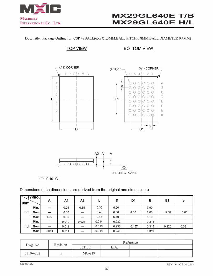
80P/N:PM1494 REV. 1.6, OCT. 30, 2013
MX29GL640E T/BMX29GL640E H/L
81P/N:PM1494 REV. 1.6, OCT. 30, 2013
MX29GL640E T/BMX29GL640E H/L
REVISION HISTORY
Revision No. Description Page Date1.0 1. Modified CFI descriptions P44~45 AUG/28/2009 2. Removed "Preliminary" title P2
1.1 1. Added WP# protected area description P2,19,22 SEP/10/2009
1.2 1. Added 70ns grade spec. and part numbers P2,49,67, NOV/10/2009 P72,73 2. Added (e.g. Vcc and CE# ramp up simultaneously) wording P70
1.3 1. Modified Figure 10. Accelerated Program Timing Diagram P58 OCT/12/2010 2. Modified "Query Command And Command Flash Memory P43 Interface (CFI) Mode" description
1.4 1. Modified sector erase time (typ.) from 0.6s to 0.5s P5,74 DEC/27/2011 2. Modified Figure 11. CE# Controlled Write Timing Waveform P62 3. Modified Figure 16. Status Polling For Write Buffer Program P26,67 4. Modified description for RoHS compliance P75,76
1.5 1. Added MAX. Total Write Buffer Time P74 AUG/16/2013 2. Modified Figure 23. PAGE READ TIMING WAVEFORM P70 3. Advanced Sector Protection/Un-Protection description update P36~41 4. Added Note 1. Query data are always presented on the lowest P46 data output Q7~Q0 only, Q8~Q15 are "0".
1.6 1. Updated parameters for DC Characteristics. P5,50 OCT/30/2013 2. Updated Erase and Programming Performance. P5,52,74 3. Content correction P36~41
82
MX29GL640E T/BMX29GL640E H/L
MACRONIX INTERNATIONAL CO., LTD. reserves the right to change product and specifications without notice.
Except for customized products which has been expressly identified in the applicable agreement, Macronix's products are designed, developed, and/or manufactured for ordinary business, industrial, personal, and/or household applications only, and not for use in any applications which may, directly or indirectly, cause death, personal injury, or severe property damages. In the event Macronix products are used in contradicted to their target usage above, the buyer shall take any and all actions to ensure said Macronix's product qualified for its actual use in accordance with the applicable laws and regulations; and Macronix as well as it’s suppliers and/or distributors shall be released from any and all liability arisen therefrom.
Copyright© Macronix International Co., Ltd. 2009~2013. All rights reserved, including the trademarks and tradename thereof, such as Macronix, MXIC, MXIC Logo, MX Logo, Integrated Solutions Provider, NBit, Nbit, NBiit, Macronix NBit, eLiteFlash, HybridNVM, HybridFlash, XtraROM, Phines, KH Logo, BE-SONOS, KSMC, Kingtech, MXSMIO, Macronix vEE, Macronix MAP, Rich Au dio, Rich Book, Rich TV, and FitCAM. The names and brands of third party referred thereto (if any) are for identification purposes only.
For the contact and order information, please visit Macronix’s Web site at: http://www.macronix.com


