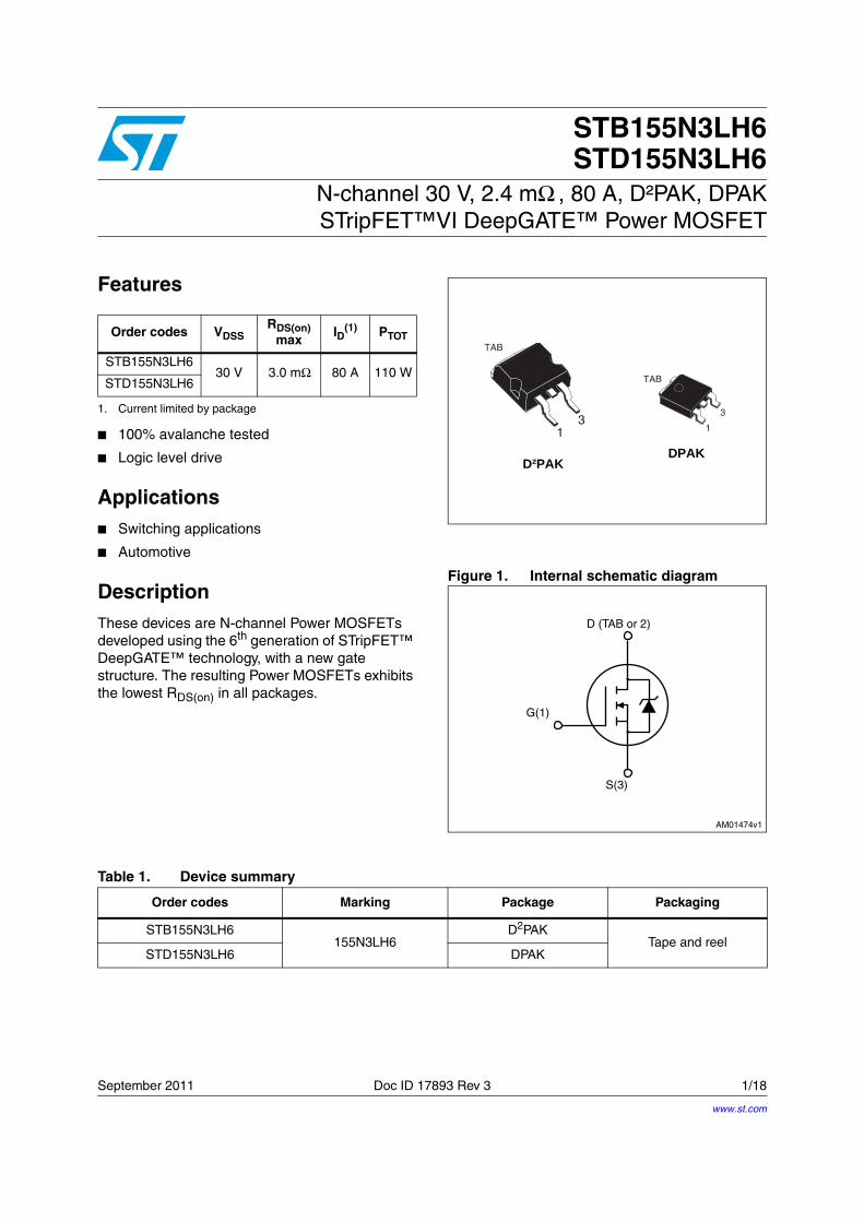
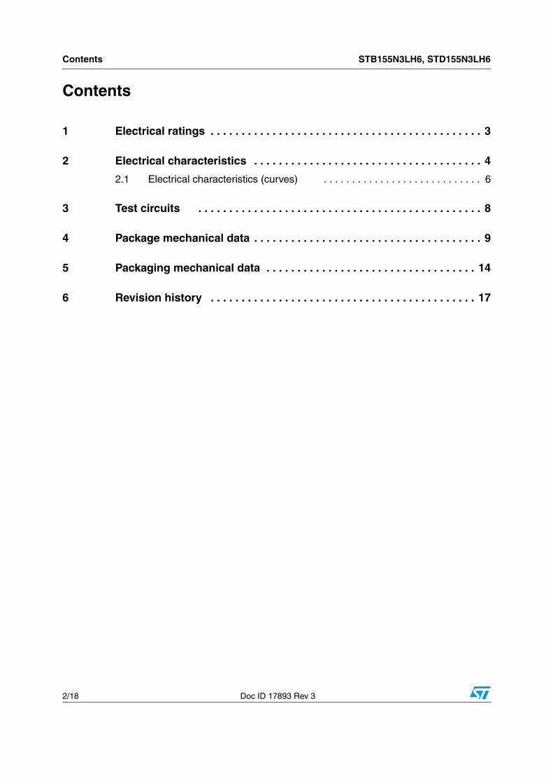
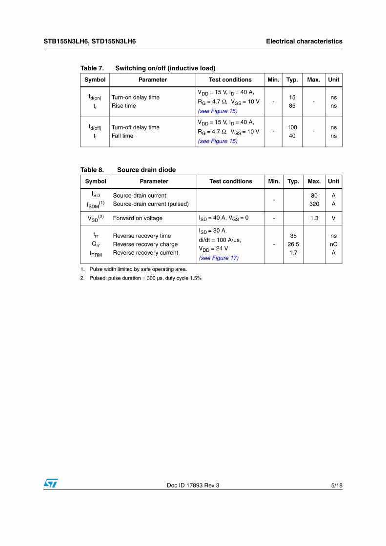
September 2011 Doc ID 17893 Rev 3 1/18 18 STB155N3LH6 STD155N3LH6 N-channel 30 V, 2.4 mΩ , 80 A, D²PAK, DPAK STripFET™VI DeepGATE™ Power MOSFET Features ■ 100% avalanche tested ■ Logic level drive Applications ■ Switching applications ■ Automotive Description These devices are N-channel Power MOSFETs developed using the 6 th generation of STripFET™ DeepGATE™ technology, with a new gate structure. The resulting Power MOSFETs exhibits the lowest R DS(on) in all packages. Figure 1. Internal schematic diagram Order codes V DSS R DS(on) max I D (1) 1. Current limited by package P TOT STB155N3LH6 30 V 3.0 mΩ 80 A 110 W STD155N3LH6 DPAK D²PAK 1 3 TAB TAB 3 1 Table 1. Device summary Order codes Marking Package Packaging STB155N3LH6 155N3LH6 D 2 PAK Tape and reel STD155N3LH6 DPAK www.st.com
Transcript
September 2011 Doc ID 17893 Rev 3 1/18
18
STB155N3LH6STD155N3LH6
N-channel 30 V, 2.4 mΩ , 80 A, D²PAK, DPAKSTripFET™VI DeepGATE™ Power MOSFET
Features
100% avalanche tested
Logic level drive
Applications Switching applications
Automotive
DescriptionThese devices are N-channel Power MOSFETs developed using the 6th generation of STripFET™ DeepGATE™ technology, with a new gate structure. The resulting Power MOSFETs exhibits the lowest RDS(on) in all packages.
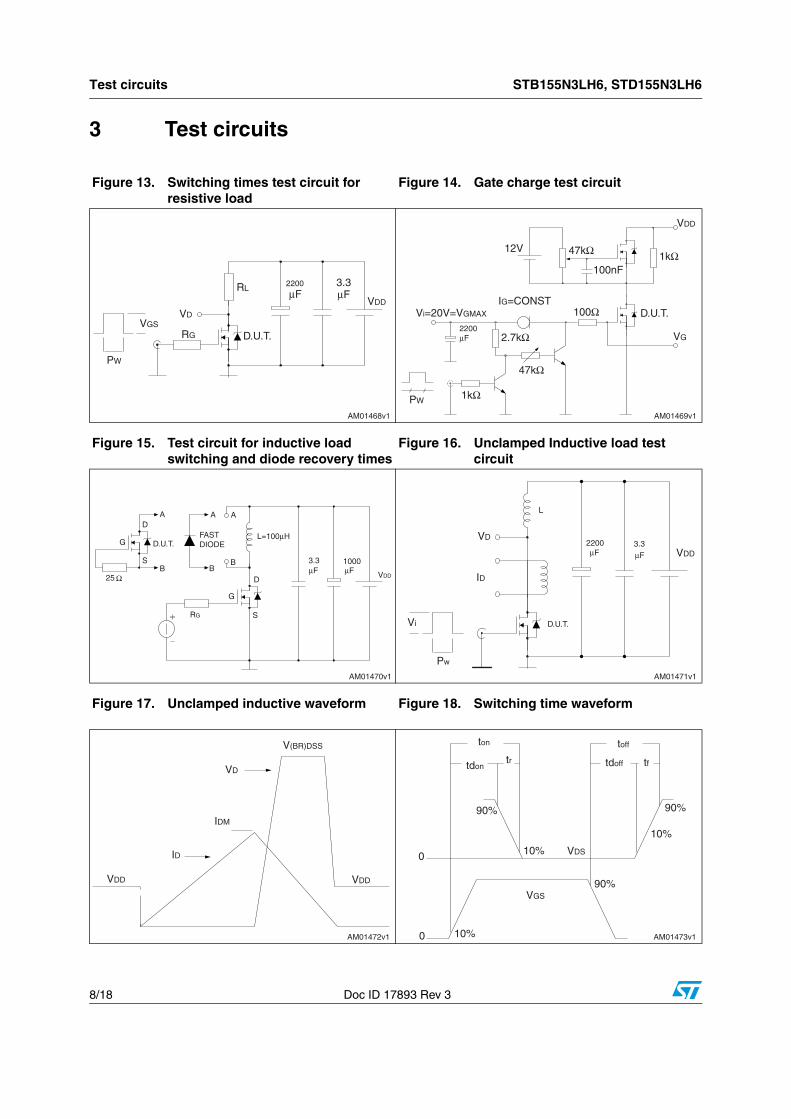
Figure 13. Switching times test circuit for resistive load
Figure 14. Gate charge test circuit
Figure 15. Test circuit for inductive load switching and diode recovery times
Figure 16. Unclamped Inductive load test circuit
Figure 17. Unclamped inductive waveform Figure 18. Switching time waveform
AM01468v1
VGS
PW
VD
RG
RL
D.U.T.
2200
µF3.3µF
VDD
AM01469v1
VDD
47kΩ 1kΩ
47kΩ
2.7kΩ
1kΩ
12V
Vi=20V=VGMAX
2200µF
PW
IG=CONST100Ω
100nF
D.U.T.
VG
AM01470v1
AD
D.U.T.
SB
G
25 Ω
A A
BB
RG
G
FASTDIODE
D
S
L=100µH
µF3.3 1000
µF VDD
AM01471v1
Vi
Pw
VD
ID
D.U.T.
L
2200µF
3.3µF VDD
AM01472v1
V(BR)DSS
VDDVDD
VD
IDM
ID
AM01473v1
VDS
ton
tdon tdoff
toff
tftr
90%
10%
10%
0
0
90%
90%
10%
VGS
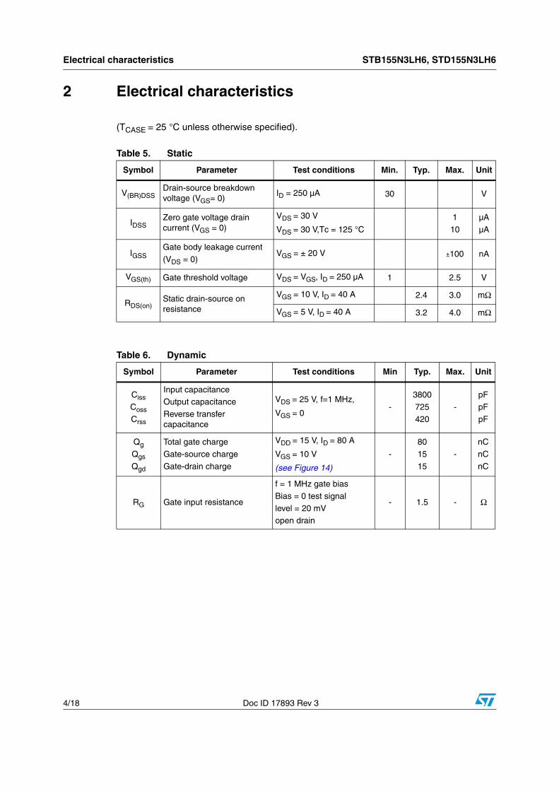
STB155N3LH6, STD155N3LH6 Package mechanical data
Doc ID 17893 Rev 3 9/18
4 Package mechanical data
In order to meet environmental requirements, ST offers these devices in different grades of ECOPACK® packages, depending on their level of environmental compliance. ECOPACK® specifications, grade definitions and product status are available at: www.st.com. ECOPACK is an ST trademark.
Package mechanical data STB155N3LH6, STD155N3LH6
10/18 Doc ID 17893 Rev 3
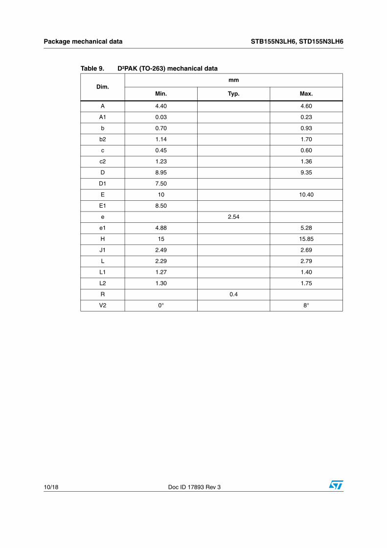
Table 9. D²PAK (TO-263) mechanical data
Dim.mm
Min. Typ. Max.
A 4.40 4.60
A1 0.03 0.23
b 0.70 0.93
b2 1.14 1.70
c 0.45 0.60
c2 1.23 1.36
D 8.95 9.35
D1 7.50
E 10 10.40
E1 8.50
e 2.54
e1 4.88 5.28
H 15 15.85
J1 2.49 2.69
L 2.29 2.79
L1 1.27 1.40
L2 1.30 1.75
R 0.4
V2 0° 8°
STB155N3LH6, STD155N3LH6 Package mechanical data
Doc ID 17893 Rev 3 11/18
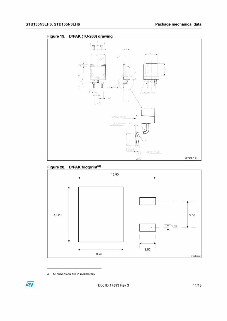
Figure 19. D²PAK (TO-263) drawing
Figure 20. D²PAK footprint(a)
a. All dimension are in millimeters
0079457_S
16.90
12.20
9.75
3.50
5.08
1.60
Footprint
Package mechanical data STB155N3LH6, STD155N3LH6
12/18 Doc ID 17893 Rev 3
Table 10. DPAK (TO-252) mechanical data
Dim.mm
Min. Typ. Max.
A 2.20 2.40
A1 0.90 1.10
A2 0.03 0.23
b 0.64 0.90
b4 5.20 5.40
c 0.45 0.60
c2 0.48 0.60
D 6.00 6.20
D1 5.10
E 6.40 6.60
E1 4.70
e 2.28
e1 4.40 4.60
H 9.35 10.10
L 1 1.50
L1 2.80
L2 0.80
L4 0.60 1
R 0.20
V2 0° 8°
STB155N3LH6, STD155N3LH6 Package mechanical data
Doc ID 17893 Rev 3 13/18
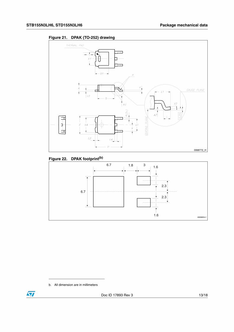
Figure 21. DPAK (TO-252) drawing
Figure 22. DPAK footprint(b)
b. All dimension are in millimeters
0068772_H
6.7
1.6
1.6
2.3
2.3
6.7 1.8 3
AM08850v1
Packaging mechanical data STB155N3LH6, STD155N3LH6
14/18 Doc ID 17893 Rev 3
5 Packaging mechanical data
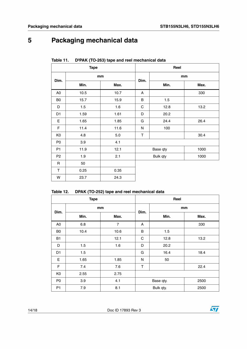
Table 11. D²PAK (TO-263) tape and reel mechanical data
Tape Reel
Dim.mm
Dim.mm
Min. Max. Min. Max.
A0 10.5 10.7 A 330
B0 15.7 15.9 B 1.5
D 1.5 1.6 C 12.8 13.2
D1 1.59 1.61 D 20.2
E 1.65 1.85 G 24.4 26.4
F 11.4 11.6 N 100
K0 4.8 5.0 T 30.4
P0 3.9 4.1
P1 11.9 12.1 Base qty 1000
P2 1.9 2.1 Bulk qty 1000
R 50
T 0.25 0.35
W 23.7 24.3
Table 12. DPAK (TO-252) tape and reel mechanical data
Tape Reel
Dim.mm
Dim.mm
Min. Max. Min. Max.
A0 6.8 7 A 330
B0 10.4 10.6 B 1.5
B1 12.1 C 12.8 13.2
D 1.5 1.6 D 20.2
D1 1.5 G 16.4 18.4
E 1.65 1.85 N 50
F 7.4 7.6 T 22.4
K0 2.55 2.75
P0 3.9 4.1 Base qty. 2500
P1 7.9 8.1 Bulk qty. 2500
STB155N3LH6, STD155N3LH6 Packaging mechanical data
Doc ID 17893 Rev 3 15/18
P2 1.9 2.1
R 40
T 0.25 0.35
W 15.7 16.3
Table 12. DPAK (TO-252) tape and reel mechanical data (continued)
Tape Reel
Dim.mm
Dim.mm
Min. Max. Min. Max.
Packaging mechanical data STB155N3LH6, STD155N3LH6
16/18 Doc ID 17893 Rev 3
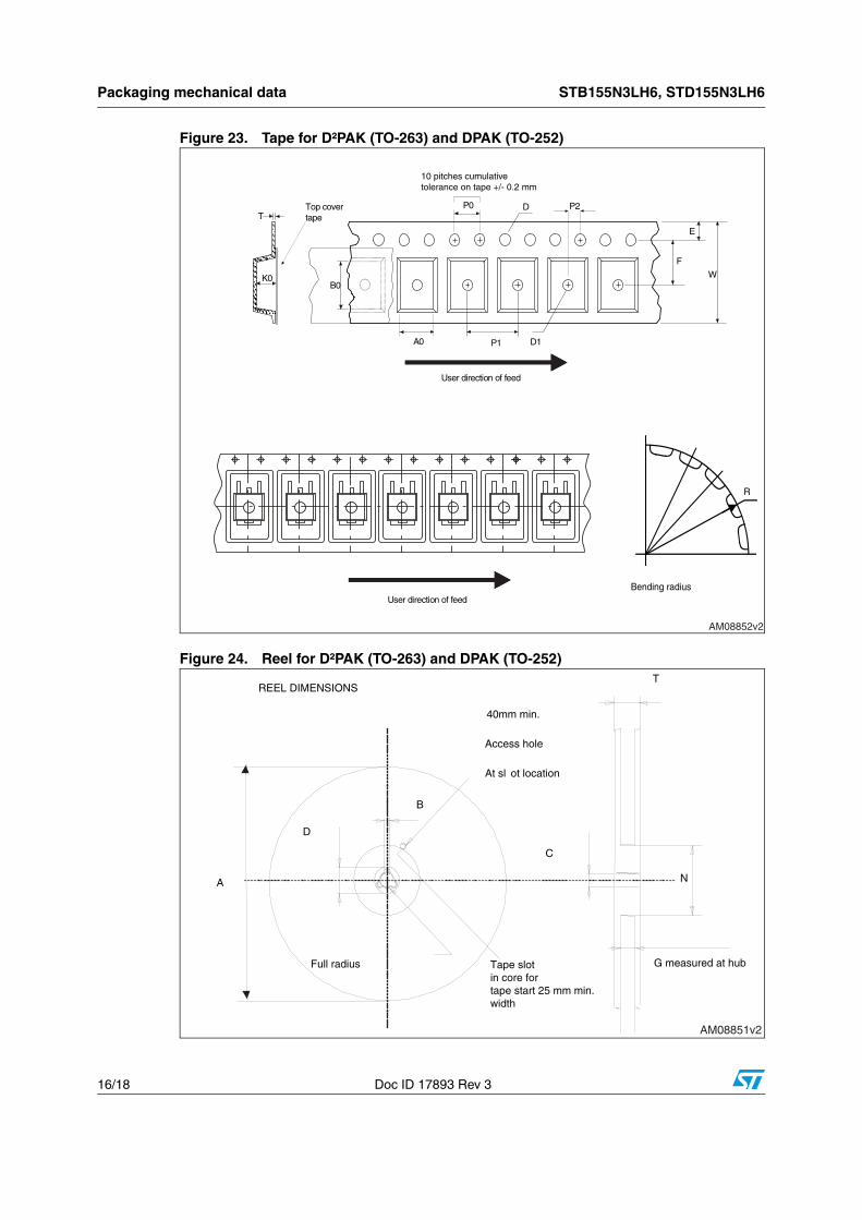
Figure 23. Tape for D²PAK (TO-263) and DPAK (TO-252)
Figure 24. Reel for D²PAK (TO-263) and DPAK (TO-252)
P1A0 D1
P0
F
W
E
D
B0K0
T
User direction of feed
P2
10 pitches cumulativetolerance on tape +/- 0.2 mm
User direction of feed
R
Bending radius
Top covertape
AM08852v2
A
D
B
Full radius G measured at hub
C
N
REEL DIMENSIONS
40mm min.
Access hole
At sl ot location
T
Tape slot in core fortape start 25 mm min.width
AM08851v2
STB155N3LH6, STD155N3LH6 Revision history
Doc ID 17893 Rev 3 17/18
6 Revision history
Table 13. Document revision history
Date Revision Changes
02-Sep-2010 1 First release.
12-Apr-2011 2 Document status promoted from preliminary data to datasheet.
27-Sep-2011 3Updated Table 1: Device summary, Figure 2: Safe operating area and Section 4: Package mechanical data.
Minor text changes.
STB155N3LH6, STD155N3LH6
18/18 Doc ID 17893 Rev 3
Please Read Carefully:
Information in this document is provided solely in connection with ST products. STMicroelectronics NV and its subsidiaries (“ST”) reserve theright to make changes, corrections, modifications or improvements, to this document, and the products and services described herein at anytime, without notice.
All ST products are sold pursuant to ST’s terms and conditions of sale.
Purchasers are solely responsible for the choice, selection and use of the ST products and services described herein, and ST assumes noliability whatsoever relating to the choice, selection or use of the ST products and services described herein.
No license, express or implied, by estoppel or otherwise, to any intellectual property rights is granted under this document. If any part of thisdocument refers to any third party products or services it shall not be deemed a license grant by ST for the use of such third party productsor services, or any intellectual property contained therein or considered as a warranty covering the use in any manner whatsoever of suchthird party products or services or any intellectual property contained therein.
UNLESS OTHERWISE SET FORTH IN ST’S TERMS AND CONDITIONS OF SALE ST DISCLAIMS ANY EXPRESS OR IMPLIEDWARRANTY WITH RESPECT TO THE USE AND/OR SALE OF ST PRODUCTS INCLUDING WITHOUT LIMITATION IMPLIEDWARRANTIES OF MERCHANTABILITY, FITNESS FOR A PARTICULAR PURPOSE (AND THEIR EQUIVALENTS UNDER THE LAWSOF ANY JURISDICTION), OR INFRINGEMENT OF ANY PATENT, COPYRIGHT OR OTHER INTELLECTUAL PROPERTY RIGHT.
UNLESS EXPRESSLY APPROVED IN WRITING BY TWO AUTHORIZED ST REPRESENTATIVES, ST PRODUCTS ARE NOTRECOMMENDED, AUTHORIZED OR WARRANTED FOR USE IN MILITARY, AIR CRAFT, SPACE, LIFE SAVING, OR LIFE SUSTAININGAPPLICATIONS, NOR IN PRODUCTS OR SYSTEMS WHERE FAILURE OR MALFUNCTION MAY RESULT IN PERSONAL INJURY,DEATH, OR SEVERE PROPERTY OR ENVIRONMENTAL DAMAGE. ST PRODUCTS WHICH ARE NOT SPECIFIED AS "AUTOMOTIVEGRADE" MAY ONLY BE USED IN AUTOMOTIVE APPLICATIONS AT USER’S OWN RISK.
Resale of ST products with provisions different from the statements and/or technical features set forth in this document shall immediately voidany warranty granted by ST for the ST product or service described herein and shall not create or extend in any manner whatsoever, anyliability of ST.
ST and the ST logo are trademarks or registered trademarks of ST in various countries.
Information in this document supersedes and replaces all information previously supplied.
The ST logo is a registered trademark of STMicroelectronics. All other names are the property of their respective owners.
Australia - Belgium - Brazil - Canada - China - Czech Republic - Finland - France - Germany - Hong Kong - India - Israel - Italy - Japan - Malaysia - Malta - Morocco - Philippines - Singapore - Spain - Sweden - Switzerland - United Kingdom - United States of America


![PAK-A-PUNCH & KEY BLANK REFERENCE - ABsupply.net · 2015-11-18 · pak-a-punch & key blank reference ... valet an1-an9282 x9/73vb pak-v1 v01 acces pak-90v 90deg ... [-p] pak-v1 v01](https://static.documents.pub/doc/80x56/5b3896967f8b9a5a518d9b59/pak-a-punch-key-blank-reference-2015-11-18-pak-a-punch-key-blank-reference.jpg)


