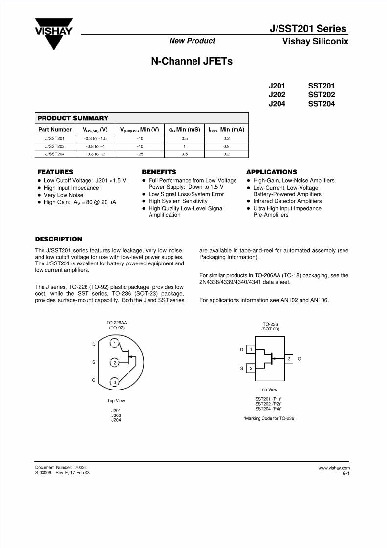
J/SST201 Series Vishay Siliconix New ProductDocument Number: 70233 S-03006—Rev. F, 17-Feb-03 www.vishay.com 6-1 N-Channel JFETs J201 SST201 J202 SST202 J204 SST204 PRODUCT SUMMARYPart Number V GS(off) (V) V (BR)GSS Min (V) g fs Min (mS) I DSS Min (mA) J/SST201 - 0.3 to - 1.5 - 40 0.5 0.2 J/SST202 - 0.8 to - 4 - 40 1 0.9 J/SST204 - 0.3 to - 2 - 25 0.5 0.2 FEA TURES BENEFITS APPLICA TIONS Low Cutoff Voltage: J201 <1.5 V High Input Impedance Very Low Noise High Gain: A V = 80 @ 20 A Full Performance from Low Voltage Power Supply: Down to 1.5 V Low Signal Loss/System Error High System Sensitivity High Quality Low-Level Signal Amplification High-Gain, Low-Noise Amplifiers Low-Current, Low-Voltage Battery-Powered Amplifiers Infrared Detector Amplifiers Ultra High Input Impedance Pre-Amplifiers DESCRIPTION The J/SST201 series features low leakage, very low noise, and low cutoff voltage for use with low-level power supplies. The J/SST201 is excellent for battery powered equipment and low current amplifiers. The J series, TO-226 (TO-92) plastic package, provides low cost, while the SST series, TO-236 (SOT-23) package, provides surface- mount capabil ity. Both the J and SST series are available in tape-and-reel for automated assembly (see Packaging Information). For similar products in TO-206AA (TO-18) packaging, see the 2N4338/4339/4340/4341 data sheet. For applications information see AN102 and AN106. TO-226AA (TO-92) Top View J201 J202 J204 D G S 1 2 3 D S G TO-236 (SOT-23) 2 3 1 Top View SST201 (P1)* SST202 (P2)* SST204 (P4)* *Marking Code for TO-236
The J/SST201 series features low leakage, very low noise,and low cutoff voltage for use with low-level power supplies.The J/SST201 is excellent for battery powered equipment andlow current amplifiers.
The J series, TO-226 (TO-92) plastic package, provides lowcost, while the SST series, TO-236 (SOT-23) package,provides surface-mount capabil ity. Both the J and SST series
are available in tape-and-reel for automated assembly (seePackaging Information).
For similar products in TO-206AA (TO-18) packaging, see the2N4338/4339/4340/4341 data sheet.
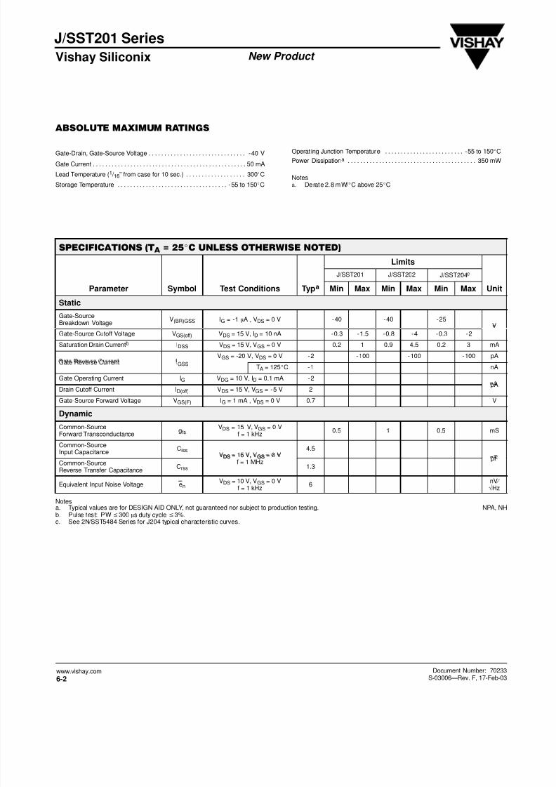
SPECIFICATIONS (T A = 25_C UNLESS OTHERWISE NOTED)
Limits
J/SST201 J/SST202 J/SST204c
Parameter Symbol Test Conditions Typa Min Max Min Max Min Max Unit
Static
Gate-SourceBreakdown Voltage
V(BR)GSS IG = - 1 mA , VDS = 0 V -40 -40 -25V
Gate-Source Cutoff Voltage VGS(off) VDS = 15 V, ID = 10 nA -0.3 -1.5 -0.8 -4 -0.3 -2
Saturation Drain Currentb IDSS VDS = 15 V, VGS = 0 V 0.2 1 0.9 4.5 0.2 3 mA
VGS = -20 V, VDS = 0 V -2 -100 -100 -100 pA
Gate Reverse Current IGSSTA = 125_C -1 nA
Gate Operating Current IG VDG = 10 V, ID = 0.1 mA -2
Drain Cutoff Current ID(off) VDS = 15 V, VGS = -5 V 2pA
Gate-Source Forward Voltage VGS(F) IG = 1 mA , VDS = 0 V 0.7 V
Dynamic
Common-SourceForward Transconductance
gfsVDS = 15 V, VGS = 0 V
f = 1 kHz0.5 1 0.5 mS
Common-SourceInput Capacitance
CissVDS = 15 V, VGS = 0 V
4.5
Common-SourceReverse Transfer Capacitance
Crss
,f = 1 MHz
1.3
pF
Equivalent Input Noise Voltage enVDS = 10 V, VGS = 0 V
f = 1 kHz6
nV ⁄ √Hz
Notesa. Typical values are for DESIGN AID ONLY, not guaranteed nor subject to production testing. NPA, NHb. Pulse test: PWv300 ms duty cyclev3%.c. See 2N/SST5484 Series for J204 typical characteristic curves.


![[SiC-En-2013-17] Challenges Regarding Parallel Connection of SiC JFETs](https://static.documents.pub/doc/80x56/577cda5a1a28ab9e78a57636/sic-en-2013-17-challenges-regarding-parallel-connection-of-sic-jfets.jpg)


