Page 1
Approved in the First Governing body
NANDHA ENGINEERING COLLEGE (An Autonomous Institution affiliated to Anna University Chennai and approved by AICTE, New Delhi)
Erode-638 052, Tamilnadu, India, Phone: 04294 – 225585
Curriculum and Syllabus
for
M.E – Applied Electronics [R13]
(This Curriculum and Syllabi are applicable to Students admitted from the academic year 2013-2014
onwards)
AUGUST 2013
Page 2
Approved in the First Governing body
NANDHA ENGINEERING COLLEGE, ERODE-52
REGULATIONS 2013
M.E. (Applied Electronics)
I TO IV SEMESTERS (FULL TIME) CURRICULUM AND SYLLABUS
SEMESTER I
THEORY
Course code
codecoCode
Course Title L T P C
13AE101 Applied Mathematics for Electronics Engineers 3 1 0 4
13AE102 Advanced Digital Signal Processing 3 0 0 3
13AE103 Advanced Digital System Design 3 0 0 3
13VL 102 VLSI Design Techniques 3 0 0 3
13AE104 Advanced Microprocessors and Micro Controllers 3 0 0 3
E1 Elective I 3 0 0 3
PRACTICAL
Course code Course Title L T P C
13AE116 Electronics Design Lab I 0 0 4 2
TOTAL 18 1 4 21
SEMESTER II
THEORY
Course code Course Title L T P C
13AE201 Analysis and Design of Analog Integrated Circuits 3 0 0 3
13AE202 Computer Architecture and Parallel Processing 3 0 0 3
13AE203 Digital Control Engineering 3 0 0 3
13AE204 Embedded Systems 3 0 0 3
E2 Elective II 3 0 0 3
E3 Elective III 3 0 0 3
PRACTICAL
Course code Course Title L T P C
13AE215 Electronics Design Lab II 0 0 4 2
TOTAL 18 0 4 20
Page 3
Approved in the First Governing body
SEMESTER III
THEORY Course code Course Title L T P C
E4 Elective IV 3 0 0 3
E5 Elective V 3 0 0 3
E6 Elective VI 3 0 0 3
PRACTICAL
Course code Course Title L T P C
13AE331 Project Work (Phase I) 0 0 12 6
TOTAL
9
0
12
15
SEMESTER IV
PRACTICAL
Course code Course Title L T P C
13AE431 Project Work (Phase II) 0 0 24 12
TOTAL
18
0
24
12
Page 4
Approved in the First Governing body
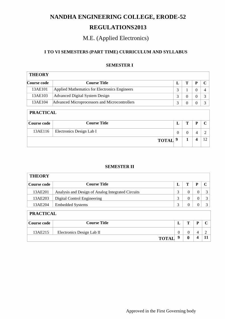
NANDHA ENGINEERING COLLEGE, ERODE-52
REGULATIONS 2013
M.E. (Applied Electronics)
I TO VI SEMESTERS (PART TIME) CURRICULUM AND SYLLABUS
SEMESTER I
THEORY
Course code
codecoCode
Course Title L T P C
13AE101 Applied Mathematics for Electronics Engineers 3 1 0 4
13AE103 Advanced Digital System Design 3 0 0 3
13AE104 Advanced Microprocessors and Microcontrollers 3 0 0 3
PRACTICAL
Course code Course Title L T P C
13AE116 Electronics Design Lab I 0 0 4 2
TOTAL 9 1 4 12
SEMESTER II
THEORY
Course code Course Title L T P C
13AE201 Analysis and Design of Analog Integrated Circuits 3 0 0 3
13AE203 Digital Control Engineering 3 0 0 3
13AE204 Embedded Systems 3 0 0 3
PRACTICAL
Course code Course Title L T P C
13AE215 Electronics Design Lab II 0 0 4 2
TOTAL 9 0 4 11
Page 5
Approved in the First Governing body
SEMESTER III
THEORY
Course code
codecoCode
Course Title L T P C
13AE102 Advanced Digital Signal Processing 3 0 0 3
13VL102 VLSI Design Techniques 3 0 0 3
E1 Elective I 3 0 0 3
TOTAL 9 0 0 9
SEMESTER IV
THEORY
Course code Course Title L T P C
13AE202 Computer Architecture and Parallel Processing 3 0 0 3
E2 Elective II 3 0 0 3
E3 Elective III 3 0 0 3
TOTAL 9 0 0 9
SEMESTER V
THEORY
Course code
codecoCode
Course Title L T P C
E4 Elective IV 3 0 0 3
E5 Elective V 3 0 0 3
E6 Elective VI 3 0 0 3
PRACTICAL
Course code Course Title L T P C
13AE331 Project Work(phase I) 0 0 12 6
TOTAL 9 0 12 6
SEMESTER VI
PRACTICAL
Course code Course Title L T P C
13AE431 Project Work (phase II) 0 0 24 12
TOTAL 0 0 24 12
Page 6
Approved in the First Governing body
LIST OF ELECTIVES M.E APPLIED ELECTRONICS
ELECTIVES
Course code Course Title L T P C
13AEX01 Digital Image Processing 3 0 0 3
13AEX02 Neural Networks and Its Applications 3 0 0 3
13AEX03 Robotics 3 0 0 3
13VL101 DSP Integrated Circuits 3 0 0 3
13VLX09 ASIC Design 3 0 0 3
13AEX04 Design and Analysis of Algorithms 3 0 0 3
13AEX05 Electromagnetic Interference and Compatibility in System Design 3 0 0 3
13AEX06 High Performance Computer Networks 3 0 0 3
13AEX07 RF system Design 3 0 0 3
13VLX02 Low Power VLSI Design 3 0 0 3
13VLX03 VLSI Signal Processing 3 0 0 3
13VLX04 Analog VLSI Design 3 0 0 3
13VL201 CAD for VLSI Circuits 3 0 0 3
13AEX08 Hardware Software Co-design 3 0 0 3
Page 7
Approved in the First Governing body
13AE101 APPLIED MATHEMATICS FOR ELECTRONIC ENGINEERS
OBJECTIVE:
The course aims at imparting the knowledge of propositions, decompositions and optimality. The
course aims at providing necessary mathematical support and confidence to tackle real life problems.
LEARNING OUTCOME:
At the end of the course the students should be able
To develop efficient algorithms for solving dynamic programming problems, to
acquire skills in handling situation involving random variable.
To learn the basics and gained the skill for specialized studies and research.
T o exposed the basic characteristic features of a queueing system and acquire skills in
analysing queueing models.
To understand the basic principles of fuzzy logic.
UNIT I:FUZZY LOGIC (9+3)
Classical logic – Multivalued logics – Fuzzy propositions – Fuzzy quantifiers..
UNIT II: MATRIX THEORY (9+3)
Some important matrix factorizations – The Cholesky decomposition – QR factorization – Least
squares method – Singular value decomposition – Toeplitz matrices and some applications.
UNIT III :ONE DIMENSIONAL RANDOM VARIABLES (9+3)
Random variables – Probability function – moments – moment generating functions and their
properties – Binomial, Poisson, Geometric, Uniform, Exponential, Gamma and Normal distributions
– Function of a Random variable.
UNIT IV: DYNAMIC PROGRAMMING (9+3)
Dynamic programming – Principle of optimality – Forward and backward recursion – Applications of
dynamic programming – Problem of dimensionality.
UNIT V:QUEUEING MODELS (9+3)
Poisson Process – Markovian queues – Single and Multi-server Models – Little‟s formula – Machine
Interference Model – Steady State analysis – Self Service queue.
TUTORIAL : 15
TOTAL : 60 Hours
REFERENCES:
1. George J. Klir and Yuan, B., Fuzzy sets and fuzzy logic, Theory and applications, Prentice Hall
of India Pvt. Ltd., 1997.
2. Moon, T.K., Sterling, W.c., Mathematical methods and algorithms for signal processing,
Pearson Education, 2000.
3. Richard Johnson, miler & Freund. , Probability and Statistics for Engineers, 7th
Ed., Prentice
– Hall of India, Private Ltd., New delhi,2007.
4. Taha, H.A., Operations Research, An introduction, 7th
Ed., Pearson education editions, Asia,
New Delhi,2002.
5. Donald Gross and carl M. Harris, Fundamentals of Queueing theory, 2nd
Ed., John Wiley and
Sons, New York,1985.
L T P C
3 1 0 4
Page 8
Approved in the First Governing body
13AE102 ADVANCED DIGITAL SIGNAL PROCESSING
OBJECTIVE:
The objective of course to provide knowledge about fundamentals of digital signal processing:
specific algorithms, processing techniques and practical considerations for implementation.
LEARNING OUTCOME:
At the end of the course the students would
Get idea about performance and limitations in digital signal processing
Know about Time-domain and Frequency-domain representation of discrete signals and
systems
Analysis of discrete systems using the z-transform
Gain knowledge about Practical aspects of FFT and DFT implementation and optimization
techniques
UNIT I: DISCRETE RANDOM SIGNAL PROCESSING (9)
Discrete Random Processes- Ensemble Averages, Stationary processes, Bias and Estimation,
Autocovariance, Autocorrelation, Parseval‟s theorem, Power Spectral Density, Spectral
factorization, Filtering Random Processes, Special types of Random Processes – ARMA, AR, MA
– Yule-Walker equations.
UNIT II:SPECTRAL ESTIMATION (9)
Estimation of spectra from finite duration signals, Nonparametric methods -Periodogram, Modified
periodogram, Bartlett, Welch and Blackman-Tukey methods, Parametric methods – ARMA, AR
and MA model based spectral estimation
UNIT III:LINEAR ESTIMATION AND PREDICTION (9)
Linear prediction – Forward and Backward prediction, Solution using Levinson-Durbin algorithm,
Solution of Prony‟s normal equations, Least mean-squared error criterion, Wiener-Khintchine
relation,Wiener filter for filtering and prediction, FIR and IIR Wiener filters, Discrete Kalman filter
UNIT IV:ADAPTIVE FILTERS (9)
FIR adaptive filters – adaptive filter based on steepest descent method- Widrow-Hopf LMS
algorithm, Normalized LMS algorithm, Adaptive channel equalization, Adaptive echo cancellation,
Adaptive noise cancellation, RLS adaptive algorithm.
UNIT V:MULTIRATE DIGITAL SIGNAL PROCESSING (9)
Mathematical description of change of sampling rate – Interpolation and Decimation, Decimation
by an integer factor, Interpolation by an integer factor, Sampling rate conversion by a rational factor,
Polyphase filter structures, Multistage implementation of multirate system, Application to subband
coding – Wavelet transform
Total = 45 Hours
REFERENCES:
1. Monson H. Hayes, „Statistical Digital Signal Processing and Modeling”, John Wiley and Sons,
Inc, Singapore,2002
2. John J. Proakis, Dimitris G. Manolakis, : Digital Signal Processing‟, Pearson Education, 2002
3. Rafael C. Gonzalez, Richard E. Woods, “ Digital Image Processing”, Pearson Education
Inc.,2nd
Ed., 2004 (For Wavelet Transform Topic).
L T P C
3 0 0 3
Page 9
Approved in the First Governing body
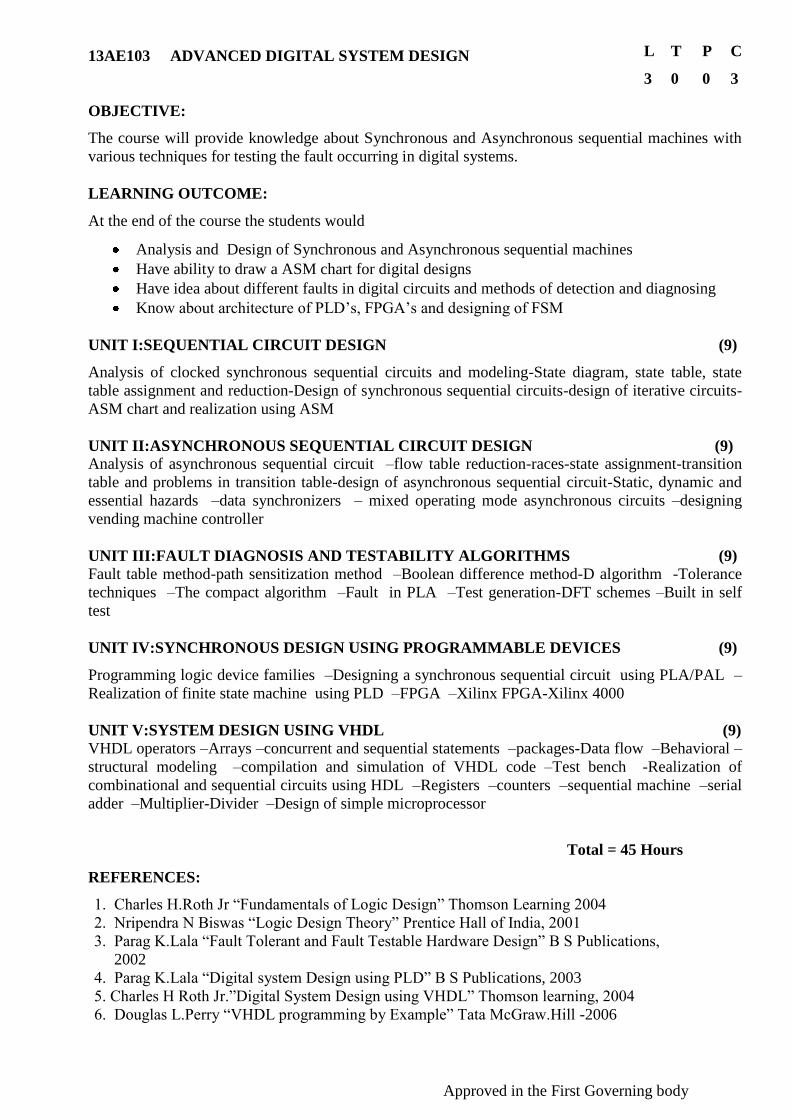
13AE103 ADVANCED DIGITAL SYSTEM DESIGN
OBJECTIVE:
The course will provide knowledge about Synchronous and Asynchronous sequential machines with
various techniques for testing the fault occurring in digital systems.
LEARNING OUTCOME:
At the end of the course the students would
Analysis and Design of Synchronous and Asynchronous sequential machines
Have ability to draw a ASM chart for digital designs
Have idea about different faults in digital circuits and methods of detection and diagnosing
Know about architecture of PLD‟s, FPGA‟s and designing of FSM
UNIT I:SEQUENTIAL CIRCUIT DESIGN (9)
Analysis of clocked synchronous sequential circuits and modeling-State diagram, state table, state
table assignment and reduction-Design of synchronous sequential circuits-design of iterative circuits-
ASM chart and realization using ASM
UNIT II:ASYNCHRONOUS SEQUENTIAL CIRCUIT DESIGN (9)
Analysis of asynchronous sequential circuit –flow table reduction-races-state assignment-transition
table and problems in transition table-design of asynchronous sequential circuit-Static, dynamic and
essential hazards –data synchronizers – mixed operating mode asynchronous circuits –designing
vending machine controller
UNIT III:FAULT DIAGNOSIS AND TESTABILITY ALGORITHMS (9)
Fault table method-path sensitization method –Boolean difference method-D algorithm -Tolerance
techniques –The compact algorithm –Fault in PLA –Test generation-DFT schemes –Built in self
test
UNIT IV:SYNCHRONOUS DESIGN USING PROGRAMMABLE DEVICES (9)
Programming logic device families –Designing a synchronous sequential circuit using PLA/PAL –
Realization of finite state machine using PLD –FPGA –Xilinx FPGA-Xilinx 4000
UNIT V:SYSTEM DESIGN USING VHDL (9)
VHDL operators –Arrays –concurrent and sequential statements –packages-Data flow –Behavioral –
structural modeling –compilation and simulation of VHDL code –Test bench -Realization of
combinational and sequential circuits using HDL –Registers –counters –sequential machine –serial
adder –Multiplier-Divider –Design of simple microprocessor
Total = 45 Hours
REFERENCES:
1. Charles H.Roth Jr “Fundamentals of Logic Design” Thomson Learning 2004
2. Nripendra N Biswas “Logic Design Theory” Prentice Hall of India, 2001
3. Parag K.Lala “Fault Tolerant and Fault Testable Hardware Design” B S Publications,
2002
4. Parag K.Lala “Digital system Design using PLD” B S Publications, 2003
5. Charles H Roth Jr.”Digital System Design using VHDL” Thomson learning, 2004
6. Douglas L.Perry “VHDL programming by Example” Tata McGraw.Hill -2006
L T P C
3 0 0 3
Page 10
Approved in the First Governing body
13VL102 VLSI DESIGN TECHNIQUES
OBJECTIVE:
The course aims to develop the skills of the students in the areas of the CMOS VLSI design
concepts as well as concerns related to combinational , sequential, Interconnect, and datapath systems
are extremely important for today‟s digital designers..
LEARNING OUTCOME:
At the end of the course the students would
To introduce the fundamental principles of VLSI circuit design.
To examine the basic building blocks of large-scale digital integrated circuits
To study the concepts on different levels of power estimation and optimization techniques
implementation of special purpose structures for complex digital systems
UNIT I:MOS TRANSISTOR THEORY AND PROCESS TECHNOLOGY (9) NMOS and PMOS transistors, Threshold voltage- Body effect- Design equations-Second order
effects. MOS models and small signal AC characteristics. Basic CMOS technology. UNIT II:INVERTERS AND LOGIC GATES (9)
NMOS and CMOS Inverters, Stick diagram, Inverter ratio, DC and transient characteristics ,
switching times, Super buffers, Driving large capacitance loads, CMOS logic structures ,
Transmission gates, Static CMOS design, dynamic CMOS design. UNIT III:CIRCUIT CHARACTERISATION AND PERFORMANCE ESTIMATION (9) Resistance estimation, Capacitance estimation, Inductance, switching characteristics, transistor sizing, power dissipation and design margining. Charge sharing .Scaling. UNIT IV:VLSI SYSTEM COMPONENTS CIRCUITS AND SYSTEM LEVEL
PHYSICAL DESIGN (9)
Multiplexers, Decoders, comparators, priority encoders, Shift registers. Arithmetic circuits – Ripple carry adders, Carry look ahead adders, High-speed adders, Multipliers. Physical design – Delay modelling ,cross talk, floor planning, power distribution. Clock distribution.
Basics of CMOS testing. UNIT V:VERILOG HARDWARE DESCRIPTION LANGUAGE (9) Overview of digital design with Verilog HDL, hierarchical modelling concepts, modules and port
definitions, gate level modelling, data flow modelling, behavioral modelling, task & functions, Test Bench.
TOTAL: 45 Hours REFRENCES:
1. Neil H.E.Weste and Kamran Eshraghian, Principles of CMOS VLSI Design, Pearson
Education Asia, 2nd
Edition,2000 2. John.P.Uymura”Introduction to VLSI Circuits and Systems”, John Wiley & Sons, Inc 2002 3. Samir Palnitkar, “Verilog HDL”, Pearson Education, 2
nd Edition, 2004.
4. Eugene D.Fabricius, Introduction to VLSI Design McGraw Hill International Editions, 1990. 5. J.Bhasker, B.S.Publications, “A Verilog HDL Primer”, 2
nd Edition, 2001.
6. Pucknell, “Basic VLSI Design”, Prentice Hall of India Publication, 1995.
L T P C
3 0 0 3
Page 11
Approved in the First Governing body
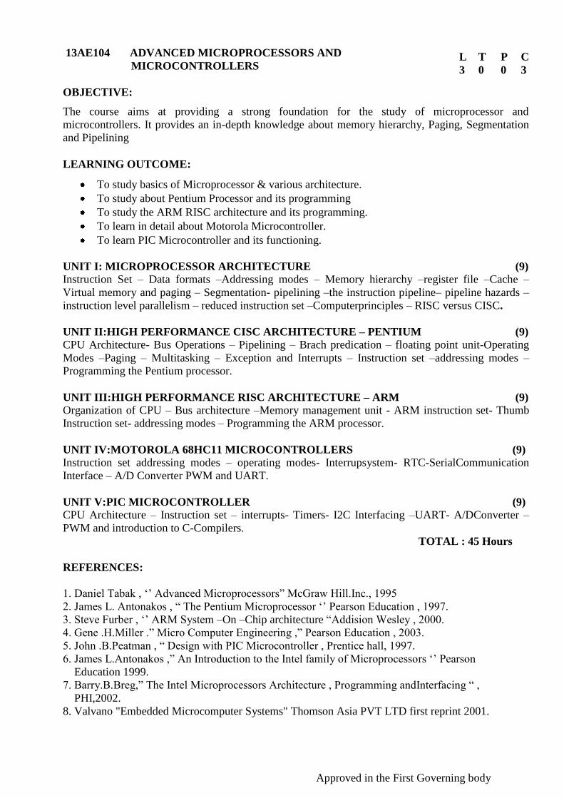
13AE104 ADVANCED MICROPROCESSORS AND
MICROCONTROLLERS
OBJECTIVE:
The course aims at providing a strong foundation for the study of microprocessor and
microcontrollers. It provides an in-depth knowledge about memory hierarchy, Paging, Segmentation
and Pipelining
LEARNING OUTCOME:
To study basics of Microprocessor & various architecture.
To study about Pentium Processor and its programming
To study the ARM RISC architecture and its programming.
To learn in detail about Motorola Microcontroller.
To learn PIC Microcontroller and its functioning.
UNIT I: MICROPROCESSOR ARCHITECTURE (9)
Instruction Set – Data formats –Addressing modes – Memory hierarchy –register file –Cache –
Virtual memory and paging – Segmentation- pipelining –the instruction pipeline– pipeline hazards –
instruction level parallelism – reduced instruction set –Computerprinciples – RISC versus CISC.
UNIT II:HIGH PERFORMANCE CISC ARCHITECTURE – PENTIUM (9)
CPU Architecture- Bus Operations – Pipelining – Brach predication – floating point unit-Operating
Modes –Paging – Multitasking – Exception and Interrupts – Instruction set –addressing modes –
Programming the Pentium processor.
UNIT III:HIGH PERFORMANCE RISC ARCHITECTURE – ARM (9)
Organization of CPU – Bus architecture –Memory management unit - ARM instruction set- Thumb
Instruction set- addressing modes – Programming the ARM processor.
UNIT IV:MOTOROLA 68HC11 MICROCONTROLLERS (9)
Instruction set addressing modes – operating modes- Interrupsystem- RTC-SerialCommunication
Interface – A/D Converter PWM and UART.
UNIT V:PIC MICROCONTROLLER (9)
CPU Architecture – Instruction set – interrupts- Timers- I2C Interfacing –UART- A/DConverter –
PWM and introduction to C-Compilers.
TOTAL : 45 Hours
REFERENCES:
1. Daniel Tabak , „‟ Advanced Microprocessors” McGraw Hill.Inc., 1995
2. James L. Antonakos , “ The Pentium Microprocessor „‟ Pearson Education , 1997.
3. Steve Furber , „‟ ARM System –On –Chip architecture “Addision Wesley , 2000.
4. Gene .H.Miller .” Micro Computer Engineering ,” Pearson Education , 2003.
5. John .B.Peatman , “ Design with PIC Microcontroller , Prentice hall, 1997.
6. James L.Antonakos ,” An Introduction to the Intel family of Microprocessors „‟ Pearson
Education 1999.
7. Barry.B.Breg,” The Intel Microprocessors Architecture , Programming andInterfacing “ ,
PHI,2002.
8. Valvano "Embedded Microcomputer Systems" Thomson Asia PVT LTD first reprint 2001.
L T P C
3 0 0 3
Page 12
Approved in the First Governing body
13AE116 ELECTRONICS DESIGN LABORATORY I
OBJECTIVE:
The course will provide the knowledge about design of logic gates, sequential & Combinational
digital systems with analysis using SPICE tool.
LEARNING OUTCOME:
At the end of the course the students would
Have knowledge about sequential & Combinational digital system designs
know about Transient and DC analysis of transistor level designs
Have skill to design and develop digital filters using DSP processors
Have experience of real time implementations
1. System design using PIC Microcontroller.
2. Implementation of Adaptive Filters, periodogram and multistage multirate
system in DSP Processor
3. Simulation of QMF using Simulation Packages
4. Modeling of Sequential Digital system using VHDL.
5. Modeling of Sequential Digital system using Verilog.
6. Design and Implementation of ALU using FPGA.
7. Simulation of NMOS and CMOS circuits using SPICE.
8. System design using 16- bit Microprocessor.
L T P C
0 0 4 2
Page 13
Approved in the First Governing body
13AE201 ANALYSIS AND DESIGN OF ANALOG INTEGRATED
CIRCUITS
OBJECTIVE:
The objective of course to provide the background and the methods for the understanding of the
operation of basic analogue CMOS cells, and how to design common functions. The emphasis is
placed on design of analogue functions specifically as part of mixed signal systems.
LEARNING OUTCOME:
At the end of the course the students would
Get idea about Active and passive components available in CMOS and their parasitic
elements of first order transistor modeling for initial manual design and the limits of
applicability
To know about Behavior and design of basic analogue circuit primitives, including
quantitative treatment of matching
CMOS Op-Amp design, from simple single ended to full differential and rail-to-rail structures
Signal and bias handling for noise immunity in mixed signal substrate
UNIT I:MODELS FOR INTEGRATED CIRCUIT ACTIVE DEVICES (9)
Depletion region of a PN junction – large signal behavior of bipolar transistors- small signalmodel of
bipolar transistor- large signal behavior of MOSFET- small signal model of theMOS transistors- short
channel effects in MOS transistors – weak inversion in MOS transistors- substrate current flow in
MOS transistor.
UNIT II:CIRCUIT CONFIGURATION FOR LINEAR IC (9)
Current sources, Analysis of difference amplifiers with active load using BJT and FET, supply and
temperature independent biasing techniques, voltage references. Output stages: Emitter follower,
source follower and Push pull output stages.
UNIT III:OPERATIONAL AMPLIFIERS (9)
Analysis of operational amplifiers circuit, slew rate model and high frequency analysis, Frequency
response of integrated circuits: Single stage and multistage amplifiers, Operational amplifier noise
UNIT IV:ANALOG MULTIPLIER AND PLL (9)
Analysis of four quadrant and variable trans conductance multiplier, voltage controlled oscillator,
closed loop analysis of PLL, Monolithic PLL design in integrated circuits: Sources of noise- Noise
models of Integrated-circuit Components – Circuit Noise Calculations – Equivalent Input Noise
Generators – Noise Bandwidth – Noise Figure and Noise Temperature
UNIT V:ANALOG DESIGN WITH MOS TECHNOLOGY (9)
MOS Current Mirrors – Simple, Cascode, Wilson and Widlar current source – CMOS Class AB
output stages – Two stage MOS Operational Amplifiers, with Cascode, MOS Telescopic- Cascode
Operational Amplifier – MOS Folded Cascode and MOS Active Cascode Operational Amplifiers.
TOTAL: 45 Hours
L T P C
3 0 0 3
Page 14
Approved in the First Governing body
REFERENCES:
1. Gray, Meyer, Lewis, Hurst, “Analysis and design of Analog IC‟s”,4th
Ed., Willey
International, 2002.
2. Behzad Razavi, “Principles of data conversion system design”, S.Chand and company
ltd, 2000
3. Nandita Dasgupata, Amitava Dasgupta,”Semiconductor Devices, Modelling and
Technology”, Prentice Hall of India pvt. ltd, 2004.
4. Grebene, Bipolar and MOS Analog Integrated circuit design”, John Wiley &
sons,Inc.,2003.
5. Phillip E.Allen Douglas R. Holberg, “CMOS Analog Circuit Design”, Second Edition-
Oxford University Press-2003
Page 15
Approved in the First Governing body
13AE202 COMPUTER ARCHITECTURE AND PARALLEL
PROCESSING
OBJECTIVE:
Computer Architecture and Parallel Processing aims at imparting the basic concepts of architecture
and organization of computers, understanding about pipelining and parallel processing techniques,
imparting knowledge about the current PC hardware
LEARNING OUTCOME:
To understand concepts of parallel processing and design choices of implementing parallel
execution within a single processor (pipeline, VLIW, and superscalar) and multiprocessor
systems.
To gain knowledge of the state of the art research topics on advanced computing systems.
UNIT I:THEORY OF PARALLELISM (9) Parallel computer models - the state of computing, Multiprocessors and Multicomputers and
Multivectors and SIMD computers, PRAM and VLSI models, Architectural development tracks.
Program and network properties- Conditions of parallelism.
UNIT II:PARTITIONING AND SCHEDULING (9) Program partitioning and scheduling, Program flow mechanisms, System interconnect architectures.
Principles of scalable performance – performance matrices and measures, Parallel processing
applications, speedup performance laws, scalability analysis and approaches.
UNIT III:HARDWARE TECHNOLOGIES (9) Processor and memory hierarchy advanced processor technology, superscalar and vector processors,
memory hierarchy technology, virtual memory technology, bus cache and shared memory - backplane
bus systems, cache memory organisations, shared memory organisations, sequential and weak
consistency models
UNIT IV:PIPELINING AND SUPERSCALAR TECHNOLOGIES (9) Parallel and scalable architectures, Multiprocessor and Multicomputers, Multivector and SIMD
computers, Scalable, Multithreaded and data flow architectures.
UNIT V:SOFTWARE AND PARALLEL PROGRAMMING (9) Parallel models, Languages and compilers, Parallel program development and environments, UNIX,
MACH and OSF/1 for parallel computers.
TOTAL: 45 Hours
L T P C
3 0 0 3
Page 16
Approved in the First Governing body
REFERENCES:
1. Kai Hwang, " Advanced Computer Architecture ", McGraw Hill International, 2001.
2. Dezso Sima, Terence Fountain, Peter Kacsuk, ”Advanced Computer architecture – A design
Space Approach” , Pearson Education , 2003.
3. John P.Shen, “Modern processor design . Fundamentals of super scalar processors”, Tata
McGraw Hill 2003.
4. Kai Hwang, “Scalable parallel computing”, Tata McGraw Hill 1998.
5. William Stallings, “ Computer Organization and Architecture”, Macmillan Publishing
Company, 1990.
6. M.J. Quinn, “ Designing Efficient Algorithms for Parallel Computers”, McGraw Hill
International, 1994.
7. Barry, Wilkinson, Michael, Allen “Parallel Programming”, Pearson Education Asia , 2002
8. Harry F. Jordan Gita Alaghband, “ Fundamentals of parallel Processing”, Pearson Education ,
2003
9. Richard Y.Kain, “ Advanced computer architecture –A systems Design Approach”, PHI, 2003.
Page 17
Approved in the First Governing body
13AE203 DIGITAL CONTROL ENGINEERING
OBJECTIVE:
To provide students with an introduction to advanced theory and techniques of control system
analysis and design, as well as some issues in their implementation, both in linear and nonlinear
framework
LEARNING OUTCOME:
At the end of the course the students would
• Understand the approximate dynamical models used in various control applications for electro-
mechanical systems
• Design the fundamental dynamics of the controllers implemented in these applications.
• Construct suitable mathematical models applicable to the design of relevant control systems.
• Further advance usage of MATLAB/SIMULINK
UNIT I:PRINCIPLES OF CONTROLLERS (9)
Review of frequency and time response analysis and specifications of control systems, need for
controllers, continues time compensations, continues time PI, PD, PID controllers, digital PID
controllers.
UNIT II:SIGNAL PROCESSING IN DIGITAL CONTROL (9)
Sampling, time and frequency domain description, aliasing, hold operation, mathematical model of
sample and hold, zero and first order hold, factors limiting the choice of sampling rate,
reconstruction.
UNIT III:MODELING AND ANALYSIS OF SAMPLED DATA CONTROL SYSTEM (9)
Difference equation description, Z-transform method of description, pulse transfer function, time
and frequency response of discrete time control systems, stability of digital control systems, Jury's
stability test, state variable concepts, first companion, second companion, Jordan canonical
models, discrete state variable models, elementary principles.
UNIT IV:DESIGN OF DIGITAL CONTROL ALGORITHM (9)
Review of principle of compensator design, Z-plane specifications, digital compensator design
using frequency response plots, discrete integrator, discrete differentiator, development of digital
PID controller, transfer function, design in the Z-plane.
UNIT V:PRACTICAL ASPECTS OF DIGITAL CONTROL ALGORITHMS (9)
Algorithm development of PID control algorithms, software implementation, implementation
using microprocessors and microcontrollers, finite word length effects, choice of data acquisition
systems, microcontroller based temperature control systems, microcontroller based motor speed
control systems.
TOTAL : 45 Hours
REFERENCES 1. M.Gopal, "Digital Control and Static Variable Methods", Tata McGraw Hill, New Delhi,
1997.
2. John J. D'Azzo, "Constantive Houpios, Linear Control System Analysis and Design", Mc
Graw Hill, 1995.
3 Kenneth J. Ayala, "The 8051 Microcontroller- Architecture, Programming and
Applications", Penram International, 2nd Ed.,1996.
L T P C
3 0 0 3
Page 18
Approved in the First Governing body
13AE204 EMBEDDED SYSTEMS
OBJECTIVE:
The course aims at providing a strong foundation for the study of Embedded system designing,
development and debugging.
LEARNING OUTCOME:
To study Embedded computers, their features and design with an example
To study Embedded architectures, design & development.
To study the networking concepts of Embedded Systems
To study various real time Embedded algorithms
UNIT I:EMBEDDED PROCESSORS (9)
Embedded Computers, Characteristics of Embedded Computing Applications, Challenges in
Embedded Computing system design, Embedded system design process-Requirements, Specification,
Architectural Design, Designing Hardware and Software Components, System Integration, Formalism
for System Design- Structural Description, Behavioral Description, Design Example: Model Train
Controller, ARM processor- processor and memory organization.
UNIT II:EMBEDDED PROCESSOR AND COMPUTING PLATFORM (9)
Data operations, Flow of Control, SHARC processor- Memory organization, Data operations, Flow of
Control, parallelism with instructions, CPU Bus configuration, ARM Bus, SHARC Bus, Memory
devices, Input/output devices, Component interfacing, designing with microprocessor development
and debugging, Design Example : Alarm Clock. Hybrid Architecture
UNIT III:NETWORKS (9)
Distributed Embedded Architecture- Hardware and Software Architectures, Networks for embedded
systems- I2C, CAN Bus, SHARC link supports, Ethernet, Myrinet, Internet, Network-Based design-
Communication Analysis, system performance Analysis, Hardware platform design, Allocation and
scheduling, Design Example: Elevator Controller
.
UNIT IV:REAL-TIME CHARACTERISTICS (9)
Clock driven Approach, weighted round robin Approach, Priority driven Approach, Dynamic Versus
Static systems, effective release times and deadlines, Optimality of the Earliest deadline first (EDF)
algorithm, challenges in validating timing constraints in priority driven systems, Off-line Versus On-
line scheduling.
UNIT V:SYSTEM DESIGN TECHNIQUES (9)
Design Methodologies, Requirement Analysis, Specification, System Analysis and Architecture
Design, Quality Assurance, Design Example: Telephone PBX- System Architecture, Ink jet printer-
Hardware Design and Software Design, Personal Digital Assistants, Set-top Boxes.
TOTAL: 45 Hours
REFERENCES:
1. Wayne Wolf, “Computers as Components: Principles of Embedded Computing System
Design”, Morgan Kaufman Publishers.
2. Jane.W.S. Liu, “Real-Time systems”, Pearson Education Asia.
3. C. M. Krishna and K. G. Shin, “Real-Time Systems” , McGraw-Hill, 1997
4. Frank Vahid and Tony Givargis, “Embedded System Design: A Unified Hardware/Software
Introduction” , John Wiley & Sons.
L T P C
3 0 0 3
Page 19
Approved in the First Governing body
13AE215 ELECTRONICS DESIGN LAB II
OBJECTIVE:
The course will provide the knowledge about system design, programming skill using various
languages like Embedded C, Assembly level Languages and HDL. It also teach implementation of
designs in FPGA/CPLD
LEARNING OUTCOME:
At the end of the course the students would
Have knowledge about system design using different software tools
know about efficient programming techniques
Have idea about Embedded System development
Have experience of real time implementations
1. System design using PLL
2. System design using CPLD
3. Alarm clock using embedded micro controller
4. Model train controller using embedded micro controller
5. Elevator controller using embedded micro controller
6. Simulation of Non adaptive Digital Control System using MAT LAB control system
toolbox
7. Simulation of Adaptive Digital Control System using MAT LAB control system toolbox
TOTAL:60 Hours
L T P C
0 0 4 2
Page 20
Approved in the First Governing body
13AEX01 DIGITAL IMAGE PROCESSING
OBJECTIVE:
Image is the main source of information acquisition and exchange of human beings, the development
of digital image processing technique involves information science, computer science, mathematics,
physics, biology and other disciplines.
LEARNING OUTCOME:
At the end of the course the students would
Processing digital image on digital hardware usually computer.
Emphasizing certain pictorial information for better clarity.
To explore characterization of image sampling and quantization with mathematical
representation
Compressing the image data for efficient utilization of storage space and transmission
bandwidth
UNIT I:DIGITAL IMAGE FUNDAMENTALS (9)
Elements of digital image processing systems, Vidicon and Digital Camera working principles,
Elements of visual perception, brightness, contrast, hue, saturation, Mach Band effect, Image
sampling, Quantization, Dither, Two dimensional mathematical preliminaries. UNIT II:IMAGE TRANSFOR (9) 1D DFT, 2D transforms - DFT, DCT, Discrete Sine, Walsh, Hadamard, Slant, Haar, KLT, SVD, Wavelet transform. UNIT III:IMAGE ENHANCEMENT AND RESTORATI (9)
Histogram modification, Noise distributions, Spatial averaging, Directional Smoothing, Median,
Geometric mean, Harmonic mean, Contraharmonic and Yp mean filters . Design of 2D FIR filters.
Image restoration - degradation model, Unconstrained and Constrained restoration, Inverse filtering-
removal of blur caused by uniform linear motion, Wiener filtering, Geometric transformations-spatial
transformations, Gray Level interpolation. .
UNIT IV:IMAGE SEGMENTATION AND RECOGNITION (9) Image segmentation - Edge detection, Edge linking and boundary detection, Region growing, Region
splitting and Merging, Image Recognition - Patterns and pattern classes, Matching by minimum
distance classifier, Matching by correlation., Neural networks-Backpropagation network and
training, Neural network to recognize shapes.
UNIT V:IMAGE COMPRESSION (9)
Need for data compression, Huffman, Run Length Encoding, Shift codes, Arithmetic coding,
Vector Quantization, Block Truncation Coding, Transform coding, JPEG standard, JPEG 2000,
EZW, SPIHT, MPEG.
TOTAL: 45 Hours
L T P C
3 0 0 3
Page 21
Approved in the First Governing body
REFERENCES:
1. Rafael C. Gonzalez, Richard E. Woods, “ Digital Image Processing”, Pearson Education,
Inc.,2nd
Ed., 2004 2. Anil K. Jain, “Fundamentals of Digital Image Processing”, Prentice Hall of India, 2002.
3. Rafael C. Gonzalez, Richard E. Woods, Steven Eddins,” Digital Image Processing using
MATLAB”, Pearson Education, Inc., 2004.
4. D.E. Dudgeon and R.M. Mersereau, “Multidimensional Digital Signal Processing”, Prentice
Hall Professional Technical Reference, 1990.
Page 22
Approved in the First Governing body
13AEX02 NEURAL NETWORKS AND ITS APPLICATIONS
OBJECTIVE:
The course aims to develop the skills of the students in the areas to track the production losses and
abnormally high maintenance cost assets, then find ways to reduce those losses or high costs..
LEARNING OUTCOME:
At the end of the course the students would
Have learnt the basics of Safety margin and loading roughness on reliability.
Have gained a well founded knowledge of modeling and simulation.
Have obtained techniques and applications of electronics and software systems.
Have grasped the concept of reliability testing and management.
UNIT I:PROBABILITY PLOTTING AND LOAD-STRENGTH INTERFERENCE (9)
Statistical distribution , statistical confidence and hypothesis testing ,probability plottingtechniques –
Weibull, extreme value ,hazard, binomial data; Analysis of load – strength interference , Safety
margin and loading roughness on reliability.
UNIT II:RELIABILITY PREDICTION, MODELLING AND DESIGN (9)
Statistical design of experiments and analysis of variance Taguchi method, Reliabilityprediction,
Reliability modeling, Block diagram and Fault tree Analysis ,petric Nets, Statespace Analysis, Monte
carlo simulation, Design analysis methods – quality functiondeployment, load strength analysis,
failure modes, effects and criticality analysis.
UNIT III:ELECTRONICS AND SOFTWARE SYSTEMS RELIABILITY (9)
Reliability of electronic components, component types and failure mechanisms, Electronic system
reliability prediction, Reliability in electronic system design; software errors, software structure and
modularity, fault tolerance, software reliability, prediction and measurement, hardware/software
interfaces.
UNIT IV:RELIABILITY TESTING AND ANALYSIS (9)
Test environments, testing for reliability and durability, failure reporting, Pareto analysis,Accelerated
test data analysis, CUSUM charts, Exploratory data analysis andproportional hazards modeling,
reliability demonstration, reliability growth monitoring.
UNIT V:MANUFACTURE AND RELIABILITY MANAGEMENT (9)
Control of production variability, Acceptance sampling, Quality control and stressscreening,
Production failure reporting; preventive maintenance strategy, Maintenanceschedules, Design for
maintainability, Integrated reliability programmes , reliability andcosts, standard for reliability,
quality and safety, specifying reliability, organization forreliability.
TOTAL: 45 Hours
REFERENCES:
1. Patrick D.T. O‟Connor, David Newton and Richard Bromley, Practical Reliability Engineering,
4th
Ed., John Wiley & Sons, 2002
2. David J. Klinger, Yoshinao Nakada and Maria A. Menendez, Von Nostrand Reinhold, New
York, "AT & T Reliability Manual",5th
Ed., 1998.
3. Gregg K. Hobbs, "Accelerated Reliability Engineering - HALT and HASS", John Wiley &
Sons, New York, 2000.
L T P C
3 0 0 3
Page 23
Approved in the First Governing body
4. Lewis, "Introduction to Reliability Engineering", 2nd
Ed., Wiley International,1996
13AEX03 ROBOTICS
OBJECTIVE:
The course aims to develop the skills of the students to ensure that the design, construction,
operation, and application of robotsas well as computer systems for their control, sensory feedback,
and information processing.
LEARNING OUTCOME:
At the end of the course the students would
Have learnt the basics of robotics with transformation matrix.
Have gained a well founded knowledge of computer vision.
Have obtained techniques of sensors,sensing devices and artificial intelligence.
Have grasped the concept of robot integration .
UNIT I:INTRODUCTION TO ROBOTICS (9)
Motion - Potential Function, Road maps, Cell decomposition and Sensor and sensor planning.
Kinematics. Forward and Inverse Kinematics - Transformation matrix and DH transformation.
Inverse Kinematics - Geometric methods and Algebraic methods. Non-Holonomic constraints.
UNIT II:COMPUTER VISION (9)
Projection - Optics, Projection on the Image Plane and Radiometry. Image Processing - Connectivity,
Images-Gray Scale and Binary Images, Blob Filling, Thresholding, Histogram. Convolution - Digital
Convolution and Filtering and Masking Techniques. Edge Detection - Mono and Stereo Vision.
UNIT III:SENSORS AND SENSING DEVICES (9)
Introduction to various types of sensor. Resistive sensors. Range sensors – Ladar (laser distance and
ranging), Sonar, Radar and Infra-red. Introduction to sensing - Light sensing, Heat sensing, Touch
sensing and Position sensing.
UNIT IV:ARTIFICIAL INTELLIGENCE (9)
Uniform Search strategies - Breadth first, Depth first, Depth limited, Iterative and deepening depth
first search and Bidirectional search. The A* algorithm . Planning - State-Space Planning , Plan-Space
Planning, Graphplan/SatPlan and their Comparison, Multi-agent planning 1, and Multi-agent planning
2, Probabilistic Reasoning - Bayesian Networks, Decision Trees and Bayes net inference
UNIT V:INTEGRATION TO ROBOT (9)
Building of 4 axis or 6 axis robot - Vision System for pattern detection - Sensors for obstacle
detection - AI algorithms for path finding and decision making
TOTAL : 45 Hours
L T P C
3 0 0 3
Page 24
Approved in the First Governing body
REFERENCES:
1. Duda, Hart and Stork, Pattern Recognition. Wiley-Interscience, 2000.
2. Mallot, Computational Vision: Information Processing in Perception and Visual Behavior.
Cambridge, MA: MIT Press, 2000.
3. Artificial Intelligence-A Modern Approach By Stuart Russell and Peter Norvig, Pearson
Education Series in Artificial Intelligence, 2004
4. Fundamentals of Robotics, Analysis and control By Robert Schilling and Craig, Hall of India
Private Limied, New Delhi, 2003.
5. Computer Vision, A modern Approach By Forsyth and Ponce, Person Education, 2003.
Page 25
Approved in the First Governing body
13VL101 DSP INTEGRATED CIRCUITS
OBJECTIVE:
To study the detail about different architecture and design of DSP integrated circuits.
LEARNING OUTCOME:
At the end of the course the students would
Have learnt the basics of DSP integrated circuits and VLSI circuit technologies
Have gained a well founded knowledge of DFT and FFT.
Have obtained FIR filters and Word length effects.
To the detail structure of different architecture
UNIT I:DSP INTEGARTED CIRCUITS AND VLSI CIRCUIT TECHNOLOGIES (9)
Standard digital signal processors, Application specific IC‟s for DSP, DSP systems, DSP system
design, Integrated circuit design. MOS transistors, MOS logic, VLSI process technologies, Trends in
CMOStechnologies.
UNIT II:DIGITAL SIGNAL PROCESSING (9)
Digital signal processing, Sampling of analog signals, Selection of sample frequency, Signal-
processing systems, Frequency response, Transfer functions, Signal flow graphs, Filter structures,
Adaptive DSP algorithms, DFT-The Discrete Fourier Transform, FFT-The Fast Fourier Transform
Algorithm, Image coding, Discrete cosine transforms.
UNIT III:DIGITAL FILTERS AND FINITE WORD LENGTH EFFECTS (9)
FIR filters, FIR filter structures, FIR chips, IIR filters, Specifications of IIR filters, Mapping of analog
transfer functions, Mapping of analog filter structures, Multirate systems,Interpolation with an integer
factor L, Sampling rate change with a ratio L/M, Multirate filters. Finite word length effects -Parasitic
oscillations, Scaling of signal levels, Round-off noise, Measuring round-off noise, Coefficient
sensitivity, Sensitivity and noise.
UNIT IV:DSP ARCHITECTURES AND SYNTHESIS OF DSP ARCHITECTURES (9)
DSP system architectures, Standard DSP architecture, Ideal DSP architectures,Multiprocessors and
multicomputers, Systolic and Wave front arrays, Shared memory architectures. Mapping of DSP
algorithms onto hardware, Implementation based on complex PEs, Shared memory architecture with
Bit –serial PEs.
UNIT V:ARITHMETIC UNITS AND INTEGRATED CIRCUIT DESIGN (9)
Conventional number system, Redundant Number system, Residue Number System, Bit-parallel and
Bit-Serial arithmetic, Basic shift accumulator, Reducing the memory size,Complex multipliers,
Improved shift-accumulator. Layout of VLSI circuits, FFT processor,DCT processor and Interpolator
as case studies. Cordic algorithm.
TOTAL : 45 Hours
REFERENCES: 1. Lars Wanhammer, “DSP Integrated Circuits”, 1999 Academic press, New York
2. A.V.Oppenheim et.al, “Discrete-time Signal Processing”, Pearson Education, 2000.
3. Emmanuel C. Ifeachor, Barrie W. Jervis, “Digital signal processing –A practical approach”,
2nd
Ed., Pearson Education, Asia.
4. Keshab K.Parhi,“VLSI Digital Signal Processing Systems design and Implementation”, John
Wiley & Sons, 1999.
L T P C
3 0 0 3
Page 26
Approved in the First Governing body
13VLX09 ASIC DESIGN
OBJECTIVE:
The course aims to develop the skills of the students in the areas of Ability to evaluate complex
conditions in which solving one problem creates other problems Use analytical methods to assess the
cost of a decision .
LEARNING OUTCOME:
At the end of the course the students would
Have learnt the basics of ASIC design flow and library design.
Have gained a well founded knowledge of logical cells and i/o cells.
Have obtained techniques of logic synthesis, simulation and testing.
Have grasped the concept of ASIC construction, floor planning, placement and routing.
UNIT I:INTRODUCTION TO ASICS, CMOS LOGIC AND ASIC LIBRARY DESIGN (9)
Types of ASICs - Design flow - CMOS transistors CMOS Design rules - Combinational Logic Cell –
Sequential logic cell - Data path logic cell - Transistors as Resistors – Transistor Parasitic
Capacitance- Logical effort –Library cell design - Library architecture .
UNIT II:PROGRAMMABLE ASICS, PROGRAMMABLE ASIC LOGIC CELLS AND
PROGRAMMABLE ASIC I/O CELLS (9)
Anti fuse - static RAM - EPROM and EEPROM technology - PREP benchmarks - Actel ACT –
Xilinx LCA –Altera FLEX - Altera MAX DC & AC inputs and outputs - Clock & Power inputs -
Xilinx I/O blocks.
UNIT III:PROGRAMMABLE ASIC INTERCONNECT, PROGRAMMABLE ASIC
DESIGN SOFTWARE AND LOW LEVEL DESIGN ENTRY (9)
Actel ACT -Xilinx LCA - Xilinx EPLD - Altera MAX 5000 and 7000 - Altera MAX 9000 – Altera
FLEX –Design systems - Logic Synthesis - Half gate ASIC -Schematic entry - Low level design
language - PLA tools -EDIF- CFI design representation.
UNIT IV:LOGIC SYNTHESIS, SIMULATION AND TESTING (9)
Verilog and logic synthesis -VHDL and logic synthesis - types of simulation -boundary scan test -
fault simulation - automatic test pattern generation.
UNIT V: ASIC CONSTRUCTION, FLOOR PLANNING, PLACEMENT
AND ROUTING (9)
System partition - FPGA partitioning - partitioning methods - floor planning - placement -physical
design flow –global routing - detailed routing - special routing - circuit extraction –DRC.
TOTAL: 45 Hours
REFERENCES:
1. M.J.S.Smith, "Application Specific Integrated Circuits, Addison-Wesley Longman Inc,1997.
2. Farzad Nekoogar and Faranak Nekoogar, From ASICs to SOCs: A Practical Approach,
PrenticeHall PTR, 2003.
3. Wayne Wolf, FPGA-Based System Design, Prentice Hall PTR, 2004.
4. R. Rajsuman, System-on-a-Chip Design and Test. Santa Clara, CA: Artech House Publishers,
2000.
5. F. Nekoogar. Timing Verification of Application-Specific Integrated Circuits
(ASICs).Prentice Hall PTR, 1999.
L T P C
3 0 0 3
Page 27
Approved in the First Governing body
13AEX04 DESIGN AND ANALYSIS OF ALGORITHMS
OBJECTIVE:
The course aims to develop the skills of the students to ensure that the paradigms and approaches
used to analyze and design algorithms and to appreciate the impact of algorithm design in practice.
LEARNING OUTCOME:
At the end of the course the students would
Have learnt the basics of Polynomial and Exponential algorithms.
Have gained a well founded knowledge of design techniques.
Have obtained techniques of searching and sorting of graph algorithms.
Have grasped the concept of parallel algorithms and genetic algorithms .
UNIT I:INTRODUCTION (9)
Polynomial and Exponential algorithms, big "oh" and small "oh" notation, exact algorithms and
heuristics, direct / indirect / deterministic algorithms, static and dynamic complexity, stepwise
refinement.
UNIT II:DESIGNTECHNIQUES (9)
Subgoals method, working backwards, work tracking, branch and bound algorithms for traveling
salesman problem and knapsack problem, hill climbing techniques, divide and conquer method,
dynamic programming, greedy methods.
UNIT III:SEARCHING AND SORTING (9)
Sequential search, binary search, block search, Fibonacci search, bubble sort, bucket sorting, quick
sort, heap sort, average case and worst case behaviour.
UNIT IV:GRAPHALGORITHMS (9)
Minimum spanning, tree, shortest path algorithms, R-connected graphs, Even's and Kleitman's
algorithms, max-flow min cut theorem, Steiglitz's link deficit algorithm.
UNIT V:SELECTEDTOPICS (9)
NP Completeness Approximation Algorithms, NP Hard Problems, Strasseu's Matrix Multiplication
Algorithms, Magic Squares, Introduction To Parallel Algorithms and Genetic Algorithms, Monte-
Carlo Methods, Amortised Analysis.
TOTAL : 45 Hours
REFERENCES:
1. Sara Baase, "Computer Algorithms : Introduction to Design and Analysis", Addison Wesley,
1988.
2. T.H.Cormen, C.E.Leiserson and R.L.Rivest, "Introduction to Algorithms", Mc Graw Hill, 1994.
3. E.Horowitz and S.Sahni, "Fundamentals of Computer Algorithms", Galgotia Publications,
1988.
4. D.E.Goldberg, "Genetic Algorithms : Search Optimization and Machine Learning", Addison
Wesley, 1989.
L T P C
3 0 0 3
Page 28
Approved in the First Governing body
13AEX05 ELECTROMAGNETIC INTERFERENCE
AND COMPATIBILITY IN SYSTEM DESIGN
OBJECTIVE:
The course aims to develop the skills of the students to ensure that equipment items or systems will
not interfere with or prevent each other's correct operation through spurious emission and absorption
of EMI.
LEARNING OUTCOME:
At the end of the course the students would
Have learnt the basics of EMI /EMC concepts.
Have gained a well founded knowledge of EMI principles.
Have obtained techniques and applications of EMI.
Have grasped the concept of EMI design of PCBs .
UNIT I:EMI/EMC CONCEPTS (9)
EMI-EMC definitions and Units of parameters; Sources and victim of EMI; Conducted and Radiated
EMI Emission and Susceptibility; Transient EMI, ESD; Radiation Hazards.
UNIT II:EMICOUPLINGPRINCIPLES (9)
Conducted, radiated and transient coupling; Common ground impedance coupling ; Common mode
and ground loop coupling ; Differential mode coupling ; Near field cable to cable coupling, cross talk
; Field to cable coupling ; Power mains and Power supply coupling.
UNIT III:EMI CONTROL TECHNIQUES (9)
Shielding, Filtering, Grounding, Bonding, Isolation transformer, Transient suppressors, Cable routing,
Signal control.
UNIT IV:EMC DESIGN OF PCBS (9)
Component selection and mounting; PCB trace impedance; Routing; Cross talk control; Power
distribution decoupling; Zoning; Grounding; VIAs connection; Terminations.
UNIT V:EMI MEASUREMENTS AND STANDARDS (9)
Open area test site; TEM cell; EMI test shielded chamber and shielded ferrite lined anechoic chamber;
Tx /Rx Antennas, Sensors, Injectors / Couplers, and coupling factors; EMI Rx and spectrum analyzer;
Civilian standards-CISPR, FCC, IEC, EN; Military standards-MIL461E/462.
TOTAL: 45 Hours
REFERENCES:
1. V.P.Kodali, “Engineering EMC Principles, Measurements and Technologies”, IEEE Press,
Newyork, 1996.
2. Henry W.Ott.,”Noise Reduction Techniques in Electronic Systems”, A Wiley InterScience
Publications, John Wiley and Sons, Newyork, 1988.
3. Bemhard Keiser, “Principles of Electromagnetic Compatibility”, 3rd Ed., Artech house,
Norwood, 1986.
4. C.R.Paul,”Introduction to Electromagnetic Compatibility” , John Wiley and Sons,Inc, 1992.
5. Don R.J.White Consultant Incorporate, “Handbook of EMI/EMC” , Vol I-V, 1988.
L T P C
3 0 0 3
Page 29
Approved in the First Governing body
13AEX06 HIGH PERFORMANCE COMPUTER NETWORKS
OBJECTIVE:
A computer network is defined as interconnected collection of autonomous computers. Computer are
said to be interconnected, if they able to exchange information. Connection is physically established
through cables, lasers, microwaves, fiber optics and communication satellite.
LEARNING OUTCOME:
Resource sharing is the main objective of the computer network.
The goal is to provide all the program, date and hardware is available to everyone on the
network without regard to the physical location of the resource and the users.
The second objective is to provide the high Reliability.
UNIT I:INTRODUCTION (9)
Review of OSI, TCP/IP; Multiplexing, Modes of Communication, Switching, Routing. SONET –
DWDM – D SL – SDN – BISDN,ATM.
UNIT II:MULTIMEDIA NETWORKING APPLICATIONS (9)
Streaming stored Audio and Video – Best effort service – protocols for real time interactive
applications – Beyond best effort – scheduling and policing mechanism – integrated services – RSVP-
differentiated services.
UNIT III:ADVANCED NETWORKS CONCEPTS (9)
VPN-Remote-Access VPN, site-to-site VPN, Tunneling to PPP, Security in VPN.MPLS operation,
Routing, Tunneling and use of FEC, Traffic Engineering, MPLS based VPN, overlay networks-P2P
connections.
UNIT IV:TRAFFIC MODELLING (8)
Little‟s theorem, Need for modeling , Poisson modeling and its failure, Non- poisson models,
Network performance evaluation.
UNIT V:NETWORK SECURITY AND MANAGEMENT (10)
Principles of cryptography – Authentication – integrity – key distribution and certification – Access
control and: fire walls – attacks and counter measures – security in many layers. Infrastructure for
network management – The internet standard management framework – SMI, MIB, SNMP, Security
and administration – ASN.
TOTAL: 45 Hours
L T P C
3 0 0 3
Page 30
Approved in the First Governing body
REFERENCES:
1. J.F. Kurose & K.W. Ross,”Computer Networking- A top down approach featuring the internet”,
Pearson, 2nd
Ed., 2003.
2. Walrand .J. Varatya, High performance communication network, Morgan Kauffman – Harcourt
Asia Pvt. Ltd. 2nd
Ed., 2000.
3. LEOM-GarCIA, WIDJAJA, “Communication networks”, TMH seventh reprint 2002.
4. Aunurag kumar, D. MAnjunath, Joy kuri, “Communication Networking”, Morgan Kaufmann
Publishers, 1ed 2004.
5. Hersent Gurle & petit, “IP Telephony, packet Pored Multimedia communication Systems”,
Pearson education 2003.
6. Fred Halsall and Lingana Gouda Kulkarni,”Computer Networking and the Internet” 5th
Ed., Pearson education
7. Nader F.Mir ,Computer and Communication Networks, 1st Ed.
8. Larry l.Peterson&Bruce S.David, “Computer Networks: A System Approach”- 1996
Page 31
Approved in the First Governing body
13AEX07 RF SYSTEM DESIGN
OBJECTIVE:
The course aims to develop the skills of the students to ensure that the Radio frequency components
and circuits form the backbone of today's mobile and satellite communications networks.
LEARNING OUTCOME:
At the end of the course the students would
Have learnt the basics of CMOS physics and architectures.
Have gained a well founded knowledge of impedance matching and amplifiers.
Have obtained techniques of feedback systems and power amplifiers.
Have grasped the concept of frequency synthesizers ,mixers and oscillators .
UNIT I:CMOS PHYSICS, TRANSCEIVER SPECIFICATIONS
AND ARCHITECTURES (9)
CMOS: Introduction to MOSFET Physics – Noise: Thermal, shot, flicker, popcorn noise Transceiver
Specifications: Two port Noise theory, Noise Figure, THD, IP2, IP3, Sensitivity, SFDR, Phase noise -
Specification distribution over a communication link Transceiver Architectures: Receiver:
Homodyne, Heterodyne, Image reject, Low IF Architectures – Transmitter: Direct upconversion, Two
step upconversion
UNIT II:IMPEDANCE MATCHING AND AMPLIFIERS (9)
S-parameters with Smith chart – Passive IC components - Impedance matching networks Amplifiers:
Common Gate, Common Source Amplifiers – OC Time constants in bandwidth estimation and
enhancement – High frequency amplifier design Low Noise Amplifiers: Power match and Noise
match – Single ended and Differential LNAs – Terminated with Resistors and Source Degeneration
LNAs.
UNIT III:FEEDBACK SYSTEMS AND POWERAMPLIFIERS (9)
Feedback Systems: Stability of feedback systems: Gain and phase margin, Root-locus techniques –
Time and Frequency domain considerations – Compensation Power Amplifiers: General model –
Class A, AB, B, C, D, E and F amplifiers – Linearisation Techniques – Efficiency boosting
techniques – ACPR metric – Design Considerations
UNIT IV:PLL AND FREQUENCY SYNTHESIZERS (9)
PLL: Linearised Model – Noise properties – Phase detectors – Loop filters and Charge pumps
Frequency Synthesizers: Integer-N frequency synthesizers – Direct Digital Frequency synthesizers
UNIT V:MIXERS AND OSCILLATORS (9)
Mixer: characteristics – Non-linear based mixers: Quadratic mixers – Multiplier based mixers: Single
balanced and double balanced mixers – subsampling mixers Oscillators: Describing Functions,
Colpitts oscillators – Resonators – Tuned Oscillators – Negative resistance oscillators – Phase noise.
TOTAL : 45 Hours
REFERENCES:
1. T.Lee, “Design of CMOS RF Integrated Circuits”, Cambridge, 2004
2. B.Razavi, “RF Microelectronics”, Pearson Education, 1997
3. Jan Crols, Michiel Steyaert, “CMOS Wireless Transceiver Design”, Kluwer Academic
Publishers, 1997
4. B.Razavi, “Design of Analog CMOS Integrated Circuits”, McGraw Hill, 2001.
L T P C
3 0 0 3
Page 32
Approved in the First Governing body
13VLX02 LOW POWER VLSI DESIGN
OBJECTIVE:
The course aims to develop the skills of the students in the areas of Testing low power very large
scale integrated (VLSI) circuits become an area of concern due to yield and reliability problems.
LEARNING OUTCOME:
At the end of the course the students would
Have learnt the basics of low power design and physics of power dissipation .
Have gained a well founded knowledge of logical level and circuit level power optimization .
Have obtained advanced techniques and special techniques for reducing power consumption in
memories.
Have grasped the concept of synthesis and software design for low power.
UNIT I:POWER DISSIPATION IN CMOS (9)
Hierarchy of limits of power – Sources of power consumption – Physics of power dissipation in
CMOS FET devices- Basic principle of low power design.
UNIT II:POWER OPTIMIZATION (9)
Logical level power optimization – Circuit level low power design – Circuit techniques for reducing
power consumption in adders and multipliers.
UNIT III:DESIGN OF LOW POWER CMOS CIRCUITS (9)
Computer Arithmetic techniques for low power systems – Reducing power consumption in memories
– Low power clock, Interconnect and layout design – Advanced techniques – Special techniques
UNIT IV:POWER ESTIMATION (9)
Power estimation techniques – Logic level power estimation – Simulation power analysis –
Probabilistic power analysis.
UNIT V:SYNTHESIS AND SOFTWARE DESIGN FOR LOW POWER (9)
Synthesis for low power –Behavioral level transforms- Software design for low power .
TOTAL: 45 Hours
L T P C
3 0 0 3
Page 33
Approved in the First Governing body
REFERENCES:
1. K.Roy and S.C. Prasad , low power CMOS VLSI circuit design, Wiley,2000
2. Dimitrios Soudris, Chirstian Pignet, Costas Goutis, designing CMOS circuits
for low power, Kluwer,2002
3. J.B. Kuo and J.H Lou, Low voltage CMOS VLSI Circuits, Wiley 1999.
4. A.P.Chandrakasan and R.W. Broadersen, Low power digital CMOS design,
Kluwer,1995.
5. Gary Yeap, Practical low power digital VLSI design, Kluwer,1998.
6. Abdellatif Bellaouar,Mohamed.I. Elmasry, Low power digital VLSI design,s Kluwer,
1995.
7. James B. Kuo, Shin – chia Lin, Low voltage SOI CMOS VLSI Devices and Circuits.
John Wiley and sons, inc 2001.
Page 34
Approved in the First Governing body
13VLX03 VLSI SIGNAL PROCESSING
OBJECTIVE:
The course aims to develop the skills of the students to ensure that VLSI signal processing, and
describes ongoing developments in the area of digital signal processing processors and architectures.
LEARNING OUTCOME:
At the end of the course the students would
Have learnt the basics of pipelining and parallel processing concepts of FIR filters.
Have gained a well founded knowledge of retiming and strength reduction.
Have obtained techniques of convolution and pipelining and parallel processing of IIR
filters.
Have grasped the concept of arithmetic architectures .
UNIT I:INTRODUCTION TO DSP SYSTEMS, PIPELINING AND PARALLEL
PROCESSING OF FIR FILTERS (9)
Introduction to DSP systems – Typical DSP algorithms, Data flow and Dependence graphs - critical
path, Loop bound, iteration bound, Longest path matrix algorithm, Pipelining and Parallel processing
of FIR filters, Pipelining and Parallel processing for low power.
UNIT II:RETIMING, ALGORITHMIC STRENGTH REDUCTION (9)
Retiming – definitions and properties, Unfolding – an algorithm for unfolding, properties of
unfolding, sample period reduction and parallel processing application, Algorithmic strength
reduction in filters and transforms – 2-parallel FIR filter, 2-parallel fast FIR filter, DCT architecture,
rank-order filters, Odd-Even merge-sort architecture, parallel rankorder filters.
UNIT III:FAST CONVOLUTION,PIPELININGANDPARALLEL PROCESSING OF IIR
FILTERS (9)
Fast convolution – Cook-Toom algorithm, modified Cook-Toom algorithm, Pipelined andparallel
recursive filters – Look-Ahead pipelining in first-order IIR filters, Look-Aheadpipelining with power-
of-2 decomposition, Clustered look-ahead pipelining, Parallel processing of IIR filters, combined
pipelining and parallel processing of IIR filters.
UNIT IV:SCALING,ROUND-OFF NOISE, BIT-LEVEL ARITHMETIC
ARCHITECTURES (9)
Scaling and round-off noise – scaling operation, round-off noise, state variabledescription of digital
filters, scaling and round-off noise computation, round-off noise inpipelined IIR filters, Bit-level
arithmetic architectures – parallel multipliers with signextension, parallel carry-ripple and carry-save
multipliers, Design of Lyon‟s bit-serialmultipliers using Horner‟s rule, bit-serial FIR filter, CSD
representation, CSDmultiplication using Horner‟s rule for precision improvement, Distributed
Arithmetic fundamentals and FIR filters
UNIT V:NUMERICAL STRENGTH REDUCTION, SYNCHRONOUS, WAVE AND
ASYNCHRONOUS PIPELINING (9)
Numerical strength reduction – subexpression elimination, multiple constant multiplication, iterative
matching, synchronous pipelining and clocking styles, clock skew in edge-triggered single phase
clocking, two-phase clocking, wave pipelining. Asynchronous pipelining bundled data versus dual
rail protocol.
TOTAL: 45 Hours
L T P C
3 0 0 3
Page 35
Approved in the First Governing body
REFERENCES:
1. Keshab K. Parhi, “ VLSI Digital Signal Processing Systems, Design and implementation “,
Wiley, Interscience, 2007.
2. U. Meyer – Baese, “ Digital Signal Processing with Field Programmable Gate Arrays”,
Springer, 2nd
Ed., 2004
Page 36
Approved in the First Governing body
13VLX04 ANALOG VLSI DESIGN
OBJECTIVE:
The course aims to develop the skills of the students to ensure that of various masks used in the
fabrication process and how the masks are used to define various features of the devices on-chip.
The course will also serve as a prerequisite for specialized studies and research.
LEARNING OUTCOME:
At the end of the course the students would
Have learnt the basics of CMOS circuit techniques and basic BICMOS circuit technique.
Have gained a well founded knowledge of filters ,converters & sensors.
Have obtained testability and VLSI interconnects.
Have grasped the concept of statistical modeling and simulation .
UNIT I:BASIC CMOS CIRCUIT TECHNIQUES, CONTINUOUS TIME AND
LOW VOLTAGE SIGNAL PROCESSING (9)
Mixed-Signal VLSI Chips-Basic CMOS Circuits-Basic Gain Stage-Gain Boosting Techniques-Super
MOSTransistor- Primitive Analog Cells-Linear Voltage-Current Converters-MOS Multipliers and
Resistors-CMOS, Bipolar and Low-Voltage BiCMOS Op- Amp Design-Instrumentation Amplifier
Design-Low Voltage Filters.
UNIT II :BASIC BICMOS CIRCUIT TECHNIQUES, CURRENT -MODE SIGNAL
PROCESSING AND NEURALINFORMATIONPROCESSING (9)
Continuous-Time Signal Processing-Sampled-Data Signal Processing-Switched-CurrentData
Converters-Practical Considerations in SI Circuits Biologically-Inspired NeuralNetworks - Floating -
Gate, Low-Power Neural Networks-CMOS Technology and Models-Design Methodology Networks-
Contrast Sensitive Silicon Retina.
UNIT III:SAMPLED-DATA ANALOG FILTERS, OVER SAMPLED A/DCONVERTERS
AND ANALOG INTEGRATEDSENSORS (9)
First-order and Second SC Circuits-Bilinear Transformation - Cascade Design-Switched-Capacitor
Ladder Filter-Synthesis of Switched-Current Filter- Nyquist rate A/D Converters-Modulators for
Over sampled A/D Conversion-First and Second Order and Multibit Sigma-Delta Modulators-
Interpolative Modulators –Cascaded Architecture-Decimation Filtersmechanical,Thermal, Humidity
and Magnetic Sensors-Sensor Interfaces..
UNIT IV:DESIGN FOR TESTABILITY AND ANALOG VLSI INTERCONNECTS (9)
Fault modelling and Simulation - Testability-Analysis Technique-Ad Hoc Methods andGeneral
Guidelines-Scan Techniques-Boundary Scan-Built-in Self Test-Analog Test Buses-Design for
Electron -Beam Testablity-Physics of Interconnects in VLSI-Scaling of Interconnects-A Model for
Estimating Wiring Density-A Configurable Architecture for Prototyping Analog Circuits..
UNIT V:STATISTICAL MODELING AND SIMULATION, ANALOG COMPUTER
AIDED DESIGN AND ANALOG AND MIXED ANALOG-DIGITALLAYOUT (9)
Review of Statistical Concepts - Statistical Device Modeling- Statistical Circuit Simulation-
Automation Analog Circuit Design-automatic Analog Layout-CMOS Transistor Layout- Resistor
Layout-Capacitor Layout-Analog Cell Layout-Mixed Analog -Digital Layout
TOTAL: 45 Hours
L T P C
3 0 0 3
Page 37
Approved in the First Governing body
REFERENCES:
1. Mohammed Ismail, Terri Fiez, “Analog VLSI signal and Information Processing ", McGraw-
Hill International Editons, 1994.
2. Malcom R.Haskard, Lan C.May, “Analog VLSI Design - NMOS and CMOS ", Prentice Hall,
1998.
3. Randall L Geiger, Phillip E. Allen, " Noel K.Strader, VLSI Design Techniques for Analog and
Digital Circuits ", Mc Graw Hill International Company, 1990.
4. Jose E.France, Yannis Tsividis, “Design of Analog-Digital VLSI Circuits for
Telecommunication and signal Processing ", Prentice Hall, 1994
Page 38
Approved in the First Governing body
13VL201 CAD FOR VLSI CIRCUITS
OBJECTIVE:
To develop the skills of the students to ensure that the process of building miniaturized electronic
circuits, consisting mainly of semiconductor devices, called transistors, on the surface of a thin
substrate of semiconductor material.
LEARNING OUTCOME:
At the end of the course the students would
Have learnt the basics of VLSI design methodologies.
Have gained a well founded knowledge of design rules.
Have obtained technique in floor planning & routing.
Have grasped the concept of simulation, modeling, and synthesis.
UNIT I:VLSI DESIGN METHODOLOGIES (9)
Introduction to VLSI Design methodologies - Review of Data structures and algorithms - Review of
VLSI Design automation tools - Algorithmic Graph Theory and Computational Complexity -
Tractable and Intractable problems - general purpose methods forcombinatorial optimization.
UNIT II:DESIGN RULES (9)
Layout Compaction - Design rules - problem formulation - algorithms for constraint graph
compaction - placement and partitioning – Circuit representation – Placement algorithms -
partitioning
UNIT III:FLOORPLANNING (9) Floor planning concepts - shape functions and floorplan sizing - Types of local routing problems -
Area routing - channel routing - global routing - algorithms for global routing.
UNIT IV:SIMULATION (9)
Simulation - Gate-level modeling and simulation - Switch-level modeling and simulation -
Combinational Logic Synthesis - Binary Decision Diagrams - Two Level Logic Synthesis.
UNIT V:MODELLING AND SYNTHESIS (9)
High level Synthesis - Hardware models - Internal representation - Allocation - assignment and
scheduling - Simple scheduling algorithm – Assignmentoproblem–Highleveltransformations.
TOTAL: 45 Hours
REFERENCES:
1. S.H. Gerez, "Algorithms for VLSI Design Automation", John Wiley & Sons,2002.
2. N.A. Sherwani, "Algorithms for VLSI Physical Design Automation", Kluwer Academic
Publishers, 2002.
L T P C
3 0 0 3
Page 39
Approved in the First Governing body
13AEX08 HARDWARE SOFTWARE CO-DESIGN
OBJECTIVE:
To develop the skills of the students to ensure that the system-level objectives by exploiting the
synergism of hardware and software through their concurrent design.
LEARNING OUTCOME:
At the end of the course the students would
Have learnt the basics of system system specification and modeling.
Have gained a well founded knowledge of hardware/software partitioning
Have obtained techniques of hardware/software co-synthesis
Have grasped the concept of design specification and verification
.
UNIT I:SYSTEM SPECIFICATIONANDMODELLING (9)
Embedded Systems , Hardware/Software Co-Design , Co-Design for System Specification and
Modelling , Co-Design for Heterogeneous Implementation – Processor Synthesis , Single-Processor
Architectures with one ASIC , Single-Processor Architectures with many ASICs, Multi-Processor
Architectures , Comparison of Co- Design Approaches , Models of Computation ,Requirements for
Embedded System Specification.
UNIT II:HARDWARE/SOFTWAREPARTITIONING (9)
The Hardware/Software Partitioning Problem, Hardware-Software Cost Estimation, Generation of the
Partitioning Graph , Formulation of the HW/SW Partitioning Problem , Optimization , HW/SW
Partitioning based on Heuristic Scheduling, HW/SW Partitioning based on Genetic Algorithms .
UNIT III:HARDWARE/SOFTWARECO-SYNTHESIS (9)
The Co-Synthesis Problem, State-Transition Graph, Refinement and Controller Generation,
Distributed System Co-Synthesis
UNIT IV:PROTO TYPING AND EMULATION (9)
Introduction, Prototyping and Emulation Techniques , Prototyping and Emulation Environments
,Future Developments in Emulation and Prototyping ,Target Architecture- Architecture Specialization
Techniques ,System Communication Infrastructure, Target Architectures and Application System
Classes, Architectures for Control-Dominated Systems, Architectures for Data-Dominated Systems
,Mixed Systems and Less Specialized Systems.
UNIT V:DESIGNSPECIFICATIONANDVERIFICATION (9)
Concurrency, Coordinating Concurrent Computations, Interfacing Components, Verification ,
Languages for System-Level Specification and Design System-Level Specification ,Design
Representation for System Level Synthesis, System Level Specification Languages, Heterogeneous
specification and multi-language cosimulation.
TOTAL : 45 Hours
L T P C
3 0 0 3
Page 40
Approved in the First Governing body
REFERENCES:
1. Ralf Niemann , “Hardware/Software Co-Design for Data Flow Dominated Embedded
Systems”, Kluwer Academic Pub, 1998.
2. Jorgen Staunstrup , Wayne Wolf ,”Hardware/Software Co-Design: Principles and Practice” ,
Kluwer Academic Pub,1997.
3. Giovanni De Micheli , Rolf Ernst Morgon,” Reading in Hardware/Software Co-Design “
Kaufmann Publishers,2001.


![Nandha devi Natarajan - 2009 to 2015 [architectural works]](https://static.documents.pub/doc/80x56/579056011a28ab900c975d1b/nandha-devi-natarajan-2009-to-2015-architectural-works.jpg)


