77
Gayathri & Yamuna NANO TECHNOLOGY

Gayathri & Yamuna
NANO TECHNOLOGY

Gayathri & Yamuna
Topics
�Introduction �Terms and Terminologies�Fabrication�Properties and Applications�Organic Nano Tubes�Inorganic Nano Tubes� Applications

Gayathri & Yamuna
Introduction
Gayathri & Yamuna
ORIGIN
The term ‘nanotechnology’ is derived from the Greek word ‘nanos’ or ‘dwarf’.

Gayathri & Yamuna
In fiction
"The Next Tenants" Arthur C. Clarke (1957)• describes tiny machines that operate on a microscale(millionth of a meter )
In the short story "How It Was when the Past Went Away" (Robert Silverberg's1969)
• describes nanotechnology being used in the construction of stereo loudspeakers, with a thousand speakers per inch
Gayathri & Yamuna
In Literature
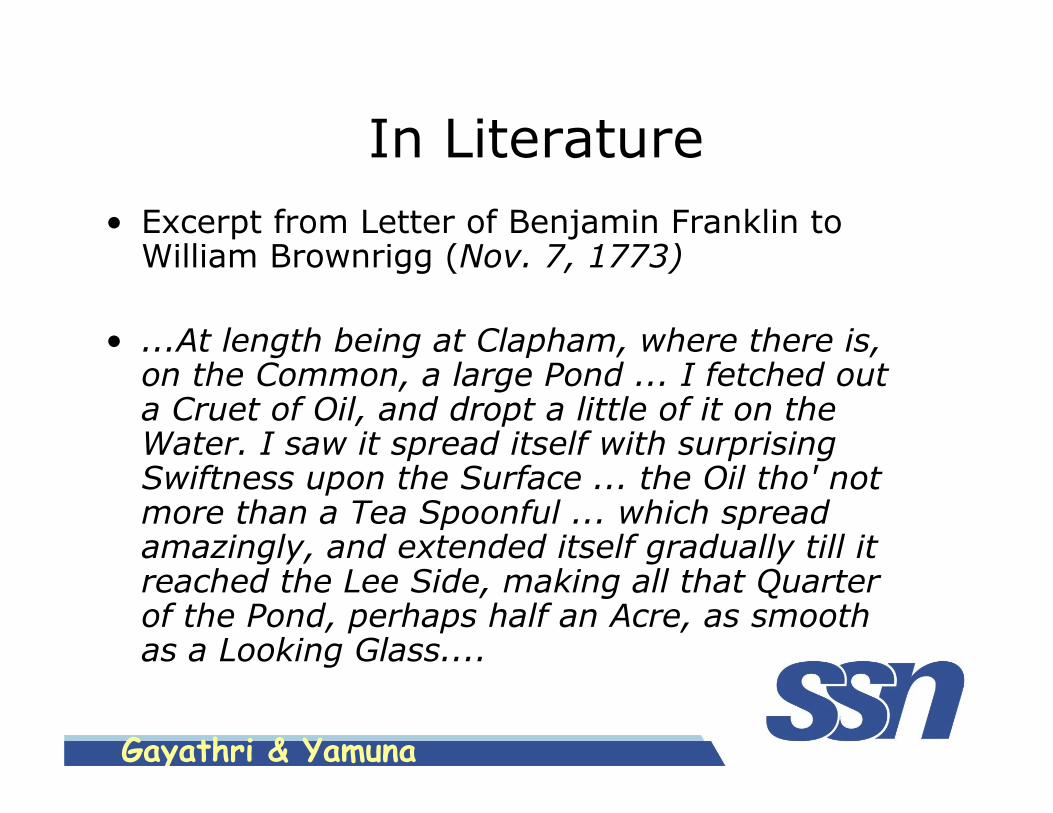
• Excerpt from Letter of Benjamin Franklin to William Brownrigg (Nov. 7, 1773)
• ...At length being at Clapham, where there is, on the Common, a large Pond ... I fetched out a Cruet of Oil, and dropt a little of it on the Water. I saw it spread itself with surprising Swiftness upon the Surface ... the Oil tho' not more than a Tea Spoonful ... which spread amazingly, and extended itself gradually till it reached the Lee Side, making all that Quarter of the Pond, perhaps half an Acre, as smooth as a Looking Glass....
Gayathri & Yamuna
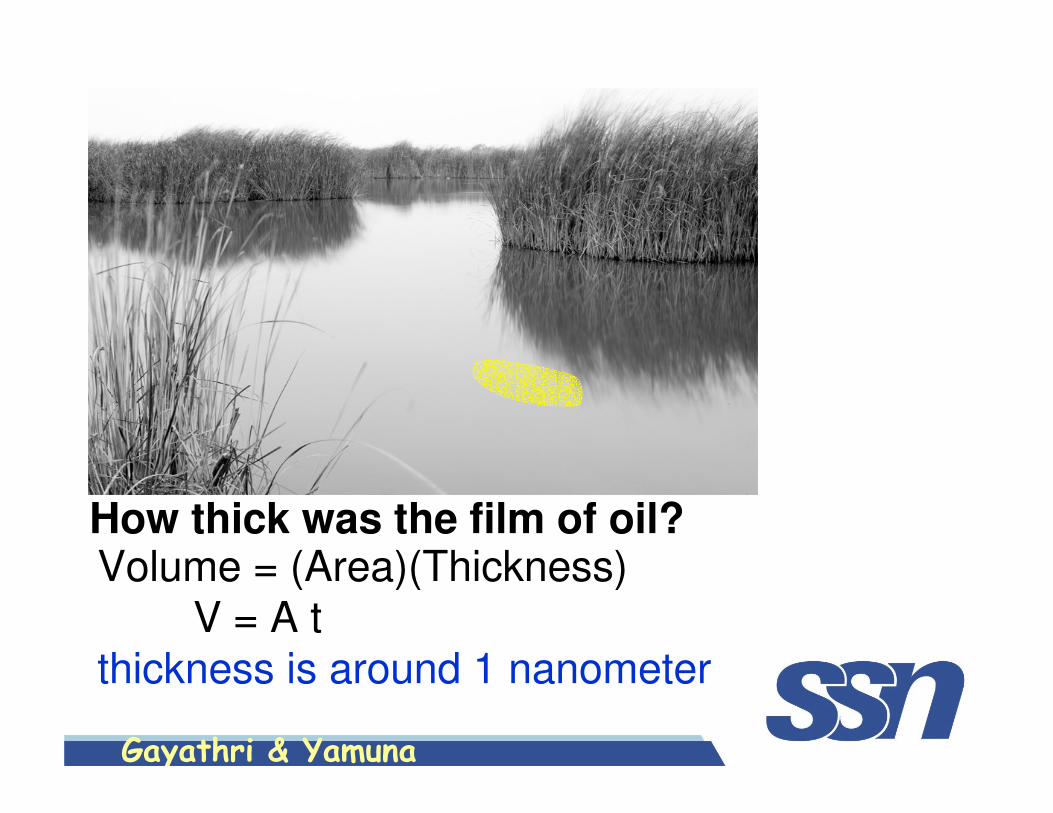
How thick was the film of oil?Volume = (Area)(Thickness)
V = A tthickness is around 1 nanometer
Gayathri & Yamuna
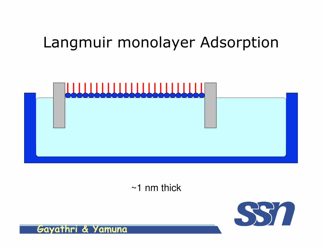
Langmuir monolayer Adsorption
~1 nm thick
Gayathri & Yamuna
Common Nano Terms
and
Terminologies

Gayathri & Yamuna
• Nano scale - at the 1-100 nm scale• Nanostructure - an object that has nano scale features
• Nano science - the behavior and properties of nanostructures
• Nanotechnology - the techniques for making and characterizing nanostructures and putting them to use
• Nano manufacturing - methods for producing nanostructures in reliable and commercially viable ways

Gayathri & Yamuna
Importance
of
Nano Technology

Gayathri & Yamuna
Nano Scale
• One nanometer (nm) is one billionth of a meter ie 10 -9 m
• 1 µm = one millionth of a meter
1 nm = one billionth of a meter
≈ 1/50,000 thickness of a hair!
(ie human hair is 50,000 nm thick)
≈ a string of 3 atoms

Gayathri & Yamuna
• To put that scale in another context, the comparative size of a meter to nano meter is same as that of earth to a glass marble

Gayathri & Yamuna
Why Nano Scale is important???
Reasons
• Matter behaves differently at micro scale and nano scale. Hence any change in nano scale influences the property at micro scale too ( i.e. brings about a corresponding change at micro scale)
Gayathri & Yamuna
• In human body dysfunction (such as Alzheimer's disease) is caused due to the malfunctioning of tiny cells (nanoscale)
• As the size of the particle decreases,
The surface area increases. This has tremendous effect on chemical reactivity
This explains that in any system , may it be living / non living , nano scale has tremendous effect on the properties and functions

Gayathri & Yamuna
How Do We See nanoparticles????
Can light microscope be used???????
Helpful, but cannot resolve below 1000 nm
How about electron microscope?????
Has a long history of usefulness at the nanoscale
A scanning probe microscope will be the best choice (SEM and TEM)

Gayathri & Yamuna
Nano Structure
• Nano-sized particles ( means zero dimension particles) exhibit drastically different or superior properties
• Nano Structures are fabricated with nano particles for example nanobatteries are 200 nm in diameter and can store sufficient energy
Gayathri & Yamuna
Nano Science
• The study of nano materials is called nanoscience
• It gives an idea about the characteristics of nano materials . They are – Smaller– Lighter– Stronger – Faster– More Durable
Gayathri & Yamuna
Do properties Change at nanolevel? Why?
Definitely Yes
For example Gold is red in colour at nano scale and yellow in colour at
micro and macro scale
Different thicknessesthicknessesthicknessesthicknesses of materials reflect and absorb light differently

Gayathri & Yamuna
What Is Nano
Technology
Gayathri & Yamuna
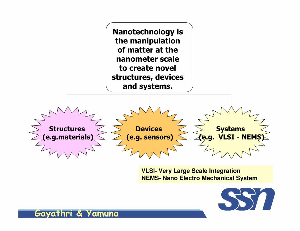
Structures (e.g.materials)
Devices (e.g. sensors)
Systems (e.g. VLSI - NEMS)
Nanotechnology is the manipulation of matter at the nanometer scale to create novel
structures, devices and systems.
VLSI- Very Large Scale IntegrationNEMS- Nano Electro Mechanical System

Gayathri & Yamuna
Fields of Application
C
ST
MT
LT
Composites
Solar
cells
Display
Food packaging
Energy/
fuel cells
Energy,
Industrial
Portable
Energy
cells
Bio-materials
Tissue/organ regen
Nanobio NEMS
Smart implants
Drugdelivery
Medicaldiagnostics
Materials
Nano-arrays
Years
Chemical
catalysts
Textiles
Coatings &
Powders
LubricantsCoatings
CosmeticsPaints
Micro-processors
Quantum computing
Simple
ICs
Memory/Storage
devices
Sensors
Displays
Devices & Microelectronics
Molecularcircuitry

Gayathri & Yamuna
Types Of Nano
Materials

Gayathri & Yamuna
• Nano particles
Tiny particles consisting of a single element / compound
Contain properties different from bulk material from which they were derived
SEM picture of AgNano particles

Gayathri & Yamuna
• Quantum Dots– Nano sized crystals– Emit light after light is incident on them
Micrograph of pyramid-shaped quantum dots grown from indium, gallium, and arsenic.Each dot is about 20 nanometers wide and 8 nanometers in height

Gayathri & Yamuna
• Buckyballs (Buckminster Fullerenes)– Molecules containing carbon atoms bound together in a hollow sphere
– Can enter cells as they pass easily through the blood stream
C60 C70

Gayathri & Yamuna
Nano Tubes
Gayathri & Yamuna
Nano
Fabrication /
Manufacturing
Gayathri & Yamuna
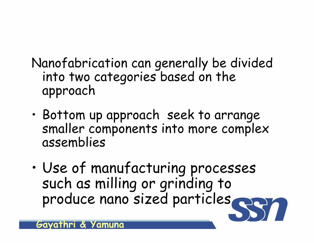
Nanofabrication can generally be divided into two categories based on the approach
• Bottom up approach seek to arrange smaller components into more complex assemblies
• Use of manufacturing processes such as milling or grinding to produce nano sized particles

Gayathri & Yamuna
• Top down approach seek to create smaller devices by using larger ones to direct their assembly
• During this approach matter is manipulated deliberately by certain chemical and/or physical processes to create materials with specific properties that are not displayed in their larger forms
• This is effected by certain chemical and/or physical processes (PVD, CVD, Etching etc.,)

Gayathri & Yamuna
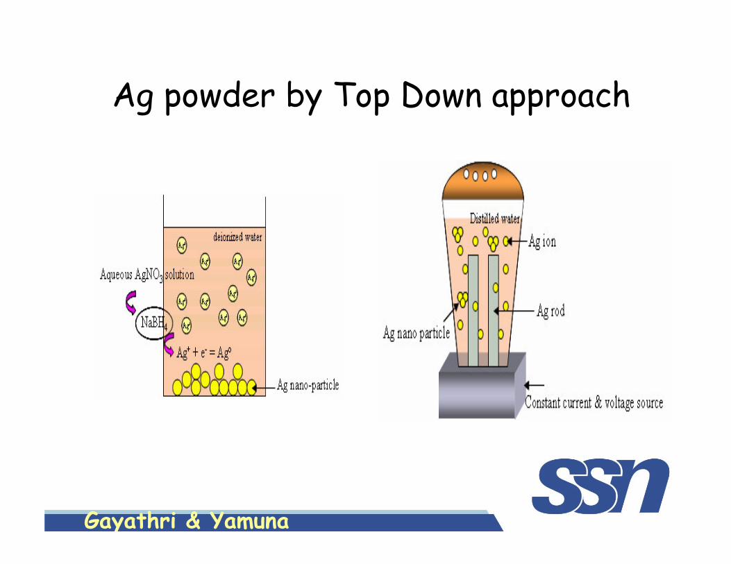
Manufacture of nano
powder
Gayathri & Yamuna
Ag powder by Top Down approach

Gayathri & Yamuna
Organic Nano
tubes
Gayathri & Yamuna
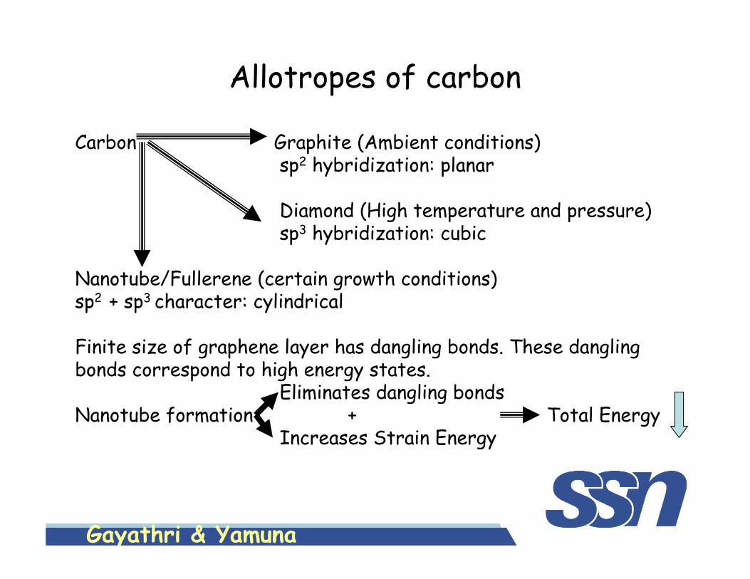
Allotropes of carbon
Carbon Graphite (Ambient conditions)sp2 hybridization: planar
Diamond (High temperature and pressure)sp3 hybridization: cubic
Nanotube/Fullerene (certain growth conditions)sp2 + sp3 character: cylindrical
Finite size of graphene layer has dangling bonds. These dangling bonds correspond to high energy states.
Eliminates dangling bonds Nanotube formation + Total Energy
Increases Strain Energy
Gayathri & Yamuna
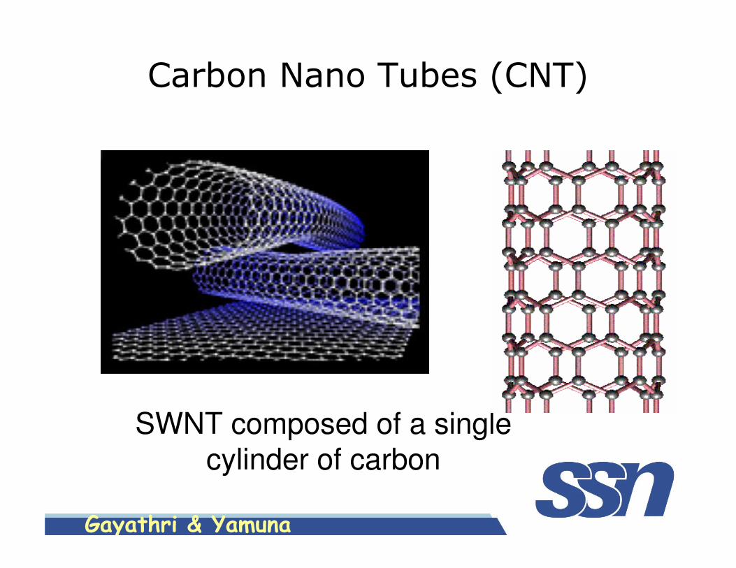
Carbon Nano Tubes (CNT)
SWNT composed of a single cylinder of carbon
Gayathri & Yamuna
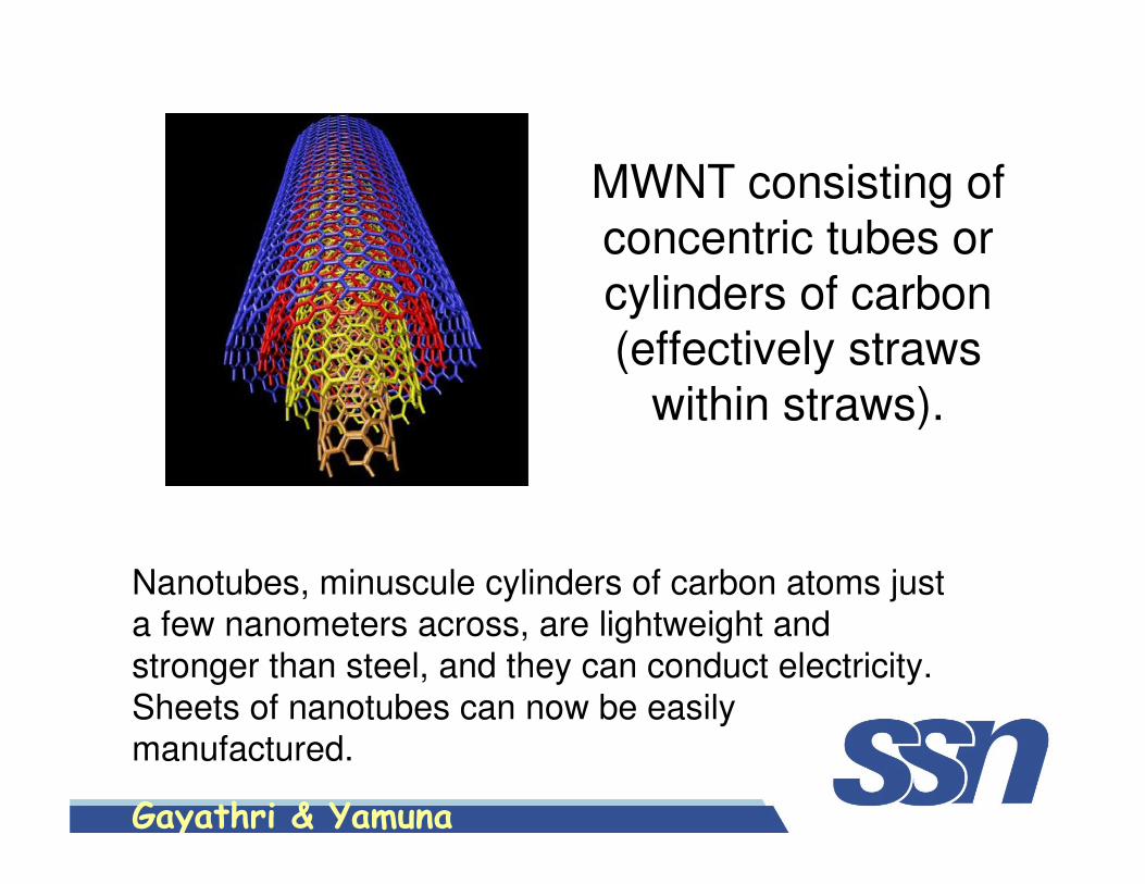
Nanotubes, minuscule cylinders of carbon atoms just a few nanometers across, are lightweight and
stronger than steel, and they can conduct electricity.
Sheets of nanotubes can now be easily manufactured.
MWNT consisting of concentric tubes or cylinders of carbon (effectively straws
within straws).

Gayathri & Yamuna
Manufacture
of CNTs
Gayathri & Yamuna
Carbon nanotubes can be manufactured using a variety of methods:
1. Laser ablation (furnace) uses a high-power laser to vaporise a graphite (sublimation point above 3,500°C )source loaded with a metal catalyst.
The carbon in the graphite reforms as predominantly single-wall nanotubes on the metal catalyst particles.
Gayathri & Yamuna
2. Arc discharge method involves an electrical discharge from a carbon-based electrode in a suitable atmosphere to produce both single and multi-wall tubes of high quality but in low quantities
3. Chemical vapour deposition (CVD) is where a hydrocarbon feedstock is reacted with a suitable metal-based catalyst in a hot furnace to ‘grow’ nanotubes which are subsequently removed from the substrate and catalyst by a simple acid wash.

Gayathri & Yamuna
Steps involved in CNT fabrication
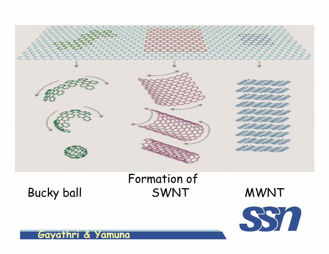
• Graphite sublimes and during condensation graphene is formed
• Graphene sheets spirals to a “Bucky ball” (1 nm)
• Graphene Rolls forming SWCNTs and /or MWNT
• SWNT – three different types
• MWNT – Two different types

Gayathri & Yamuna
Gayathri & Yamuna
Formation ofBucky ball SWNT MWNT

Gayathri & Yamuna
Two types of Carbon Nanotubes
Multi-Walled CNTSingle-Walled CNTAnimation shows formation of different conformations of

Gayathri & Yamuna
Conformations of SWNTs
Top To Bottom
Arm Chair
Side To Side
ZigZag
Corner To Corner Chiral(spiral)

Gayathri & Yamuna
• Practically every manufacturer currently uses catalytic chemical vapour deposition (CVD) to make their tubes
• This involves growing the CNTs by passing a carbon-based gas, such as methane or ethylene, over Fe/ Ni / Co catalyst at 550 – 750 oC (adsorption principle)
• The CNTs are recovered by washing with dilute mineral acid
• MWNT are easily produced by this method
Gayathri & Yamuna
SWNT
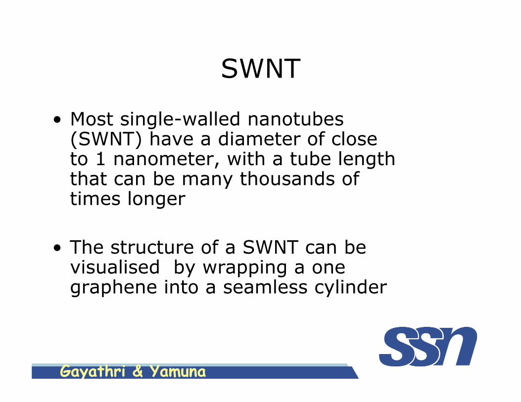
• Most single-walled nanotubes(SWNT) have a diameter of close to 1 nanometer, with a tube length that can be many thousands of times longer
• The structure of a SWNT can be visualised by wrapping a one graphene into a seamless cylinder
Gayathri & Yamuna
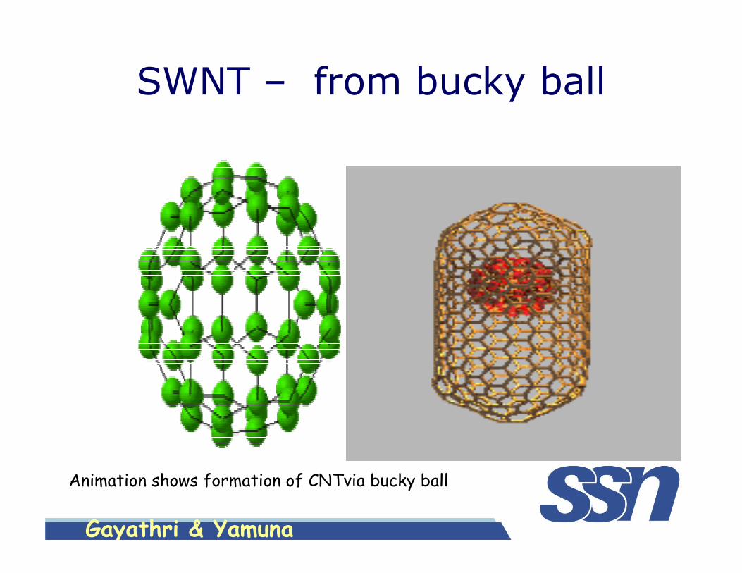
SWNT – from bucky ball
Animation shows formation of CNTvia bucky ball

Gayathri & Yamuna
This animation of a rotating SWNT shows its 3D structure and the channel in the SWNT

Gayathri & Yamuna
Single-walled nanotubes are a very important variety of carbon nanotube because they exhibit important electric properties due to their various conformations, that are not shared by the multi-walled carbon nanotube (MWNT)
In other words SWNT are superior to MWNTs

Gayathri & Yamuna
MWNT
• Multi-walled nanotubes (MWNT) consist of multiple layers of graphene rolled in on themselves to form a tube shape
• The interlayer distance in multi-walled nanotubes is close to the distance between graphene layers in graphite, approximately 3.3 Å

Gayathri & Yamuna
• There are two models which can be used to describe the structures of multi-walled nanotubes
Russian doll model Parchment Or Swiss Roll model

Gayathri & Yamuna
Russian Doll Model of Rolling
In this model , sheets of graphite are arranged in concentric cylinders

Gayathri & Yamuna
In this model single sheet of graphite is rolled in around itself, resembling a scroll of parchment or a rolled up newspaper
Parchment Model

Gayathri & Yamuna
Properties
Of
CNTs

Gayathri & Yamuna
• Carbon nano tubes are cylindrical structures usually less than 30 nanometers in diameter and several microns long
• Their aspect ratio (length-to-diameter ratio) is in millions (10,000,000 To 40,000,000 )
• CNTs are hydrophobic

Gayathri & Yamuna
• The chemical bonding of nanotubes is composed entirely of sp2 bonds (similar to graphite)
• Nanotubes naturally align themselves into "ropes" held together by Van der Waals forces(this too like graphite)
• No other element in the periodic table bonds to itself in an extended network with the strength of the carbon-carbon bond

Gayathri & Yamuna
Hence they exhibit extraordinary strength and unique electrical properties, and are efficient conductors of heat
• Out of the two types of CNTs , SWCNTs are endowed with exceptionally high electrical and thermal conductivity, strength, stiffness, and toughness
• It is interesting to note that various types of CNTs resemble in their thermal property but differ in their electrical properties

Gayathri & Yamuna
Conductivity • CNTs conductivity has been shown to be a function of their conformation (degree of twist), as well as their diameter
• Their conductivity is six times more and current density is 1000times greater than that of Cu
• Their conductance lies between metallic and semi-conducting materials
• SWNTs are better conductors than MWNTs

Gayathri & Yamuna
Thermal conductivity and Expansion
CNTs may be the best heat-conducting material man has ever known
Ultra-small SWNTs have even been shown to exhibit superconductivity below 20°K
They exhibit almost zero in-plane thermal expansion but large inter-plane expansion
Gayathri & Yamuna
Strength and Elasticity
SWNTs are stiffer than steel (6 folds greater) and are very resistant to damage from physical forces (ie excellent wear resistant)
This property makes CNTs very useful as probe tips for high-resolution scanning probe microscopes
Gayathri & Yamuna
Applications
Of
CNTs

Gayathri & Yamuna
• SWNTs have the highest Young’s modulus ( about 1 TPa) if normalized to their diameter and, therefore, all types of CNTs have attracted much interest for low weight structural composites
• It is used to manufacture stronger and lighter tennis rackets, bike parts, golf balls, golf clubs, golf shaft and baseball bats
• It is used as space elevator
CNT in sports and Space

Gayathri & Yamuna
• The high aspect ratio also makes CNTs ideal field-emission material ( FE is the emission of electrons from a solid under an intense electric field)
• Si or W tips were initially used.• CNTs have an advantage over Si or W tips in that their strong, they are physically inert to sputtering, chemically inert to poisoning, and can carry a huge current density of 109A/cm2 before electro migration
CNT in Electrical devices

Gayathri & Yamuna
• CNTs are used as an alternative to tungsten filaments in incandescent lamps
• The low resistance of CNT compared to activated carbon, greatly increase its power density
• Carbon nano fibers are presently being used to increase the conductivity of porous carbon electrodes and thus improve their power density
CNTs in Batteries and Storage devices
Gayathri & Yamuna
• Due to its high Conductivity it finds application as “quantum wires” and as electrode in fuel cell (instead of Pt electrode)
• The large surface area and tubular structure of CNTs suggest that capillarity effects are important. Thus, CNTs is useful for the storage of hydrogen, a key aspect of the clean energy economy
Gayathri & Yamuna
• Films of carbon nanotubes are used to replace indium tin oxide (ITO) in LCDs, touch screens, and photovoltaic devices
• Nanotube films are also used in displays for computers, cell phones, PDAs, and ATMs
CNT in Electronics

Gayathri & Yamuna
CNT in Smart Garments
• CNTs are used in the manufacture of Water proof and Tear resistant clothes
• It also used to manufacture Combat Jackets , worn by special patients for continuous monitoring

Gayathri & Yamuna
•It is mixed with concrete to increase the tensile strength, and halt crack propagation in huge structures
• Carbon nanotubes are used to replace steel in suspension bridges
•CNTs are used in commercial electric motor brushes
•It is used to fabricate nano gears and nano
bearings used in nano machines
CNT as Structural Material
Gayathri & Yamuna
CNT in Pollution Abatement
• Nanotube membranes are used for filtering carbon dioxide from power plant emissions
• It is used to remove salts from water ( possibly desalination purpose in future)
• It is also used to fill radio active substance before disposing under sea

Gayathri & Yamuna
• Of late CNTs are used as Biosensors and Biomedical implants due to its biocompatibility
• Soluble nano tubes are used in drug delivery systems
• Functionalized carbon nanotubes have been used to deliver proteins, nucleic acids, drugs, antibodies and other therapeutics
CNTs in Medical Field

Gayathri & Yamuna
CNTs as catalyst/ CNT in Chemical IndustryRole of CNT in catalysis
•Industry currently uses transition metal oxide catalysts (such as V2O5 / MgO ) to produce butadiene and other alkenes from butane
•By oxidising the surface of carbon nanotubesand adding a dash of phosphorous, stable catalyst was created that could effectively strip hydrogen from butane gas more selectively, and under milder reaction conditions, than the above method

Gayathri & Yamuna
Butane1,3- butadiene
P-oCNT ≡ P+ oxidised CNT

Gayathri & Yamuna
Other applications
• MWNTs coated with magnetite are used as magnets
• Nano tube composites are used as antistatic shielding on airplane wings and fuselages

Gayathri & Yamuna
• Polyacrylic acid-grafted MWNTs acts like a resin to recover / reclaim precious metals (Ag and Au) from their aqueous solution (mechanism is similar to deionisation)
Gayathri & Yamuna
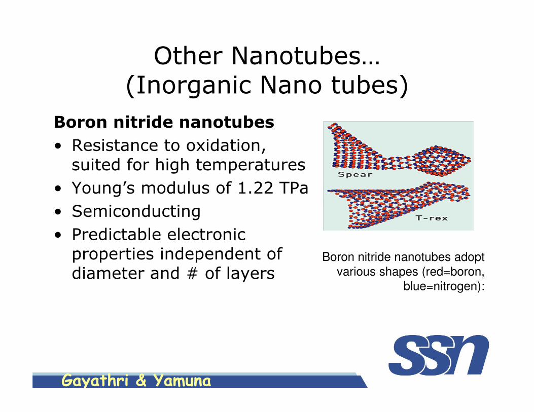
Other Nanotubes…(Inorganic Nano tubes)
Boron nitride nanotubes
• Resistance to oxidation, suited for high temperatures
• Young’s modulus of 1.22 TPa
• Semiconducting
• Predictable electronic properties independent of diameter and # of layers
Boron nitride nanotubes adopt
various shapes (red=boron,
blue=nitrogen):

Gayathri & Yamuna
SiC nanotubes
• Resistance to oxidation
• Suitable for harsh environments
• Can functionalize surface Si atoms
SiC nanotubes grown at NASA Glenn:

Gayathri & Yamuna
Any Queries?


