38
http://www.iap.uni-jena.de/multiphoton Nanomaterials and their Optical Applications Winter Semester 2012 Lecture 05 [email protected]
[email protected] Lecture 05 http://www.iap.uni-jena.de/multiphoton
Nanomaterials and their Optical Applications Winter Semester 2012
Lecture 05
[email protected] Lecture 05 http://www.iap.uni-jena.de/multiphoton
Nanomaterials and their Optical Applications Winter Semester 2012
Lecture 05
No lecture on Monday December 17
[email protected] Lecture 05
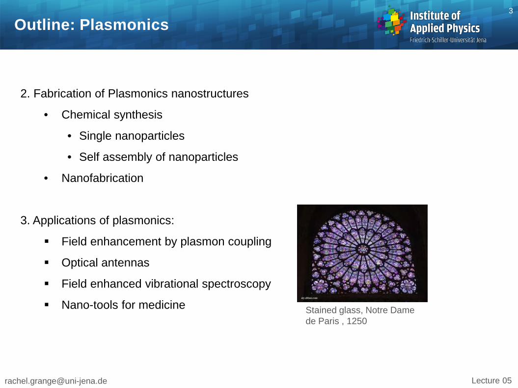
Outline: Plasmonics 3
2. Fabrication of Plasmonics nanostructures
• Chemical synthesis
• Single nanoparticles
• Self assembly of nanoparticles
• Nanofabrication
3. Applications of plasmonics:
Field enhancement by plasmon coupling
Optical antennas
Field enhanced vibrational spectroscopy
Nano-tools for medicine
Stained glass, Notre Dame de Paris , 1250
[email protected] Lecture 05
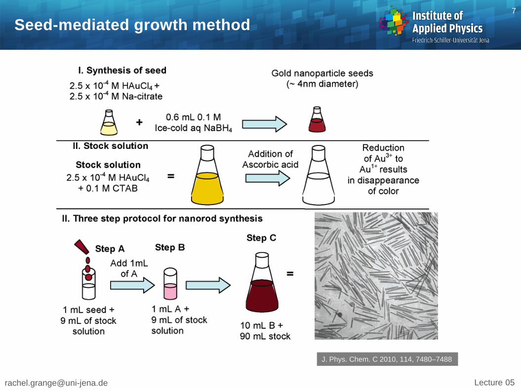
Liquid chemical synthesis 4
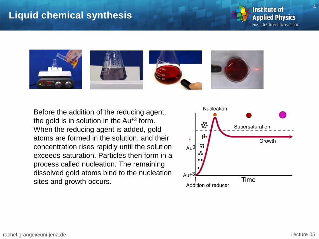
Before the addition of the reducing agent, the gold is in solution in the Au+3 form. When the reducing agent is added, gold atoms are formed in the solution, and their concentration rises rapidly until the solution exceeds saturation. Particles then form in a process called nucleation. The remaining dissolved gold atoms bind to the nucleation sites and growth occurs.
[email protected] Lecture 05
Liquid chemical synthesis 5
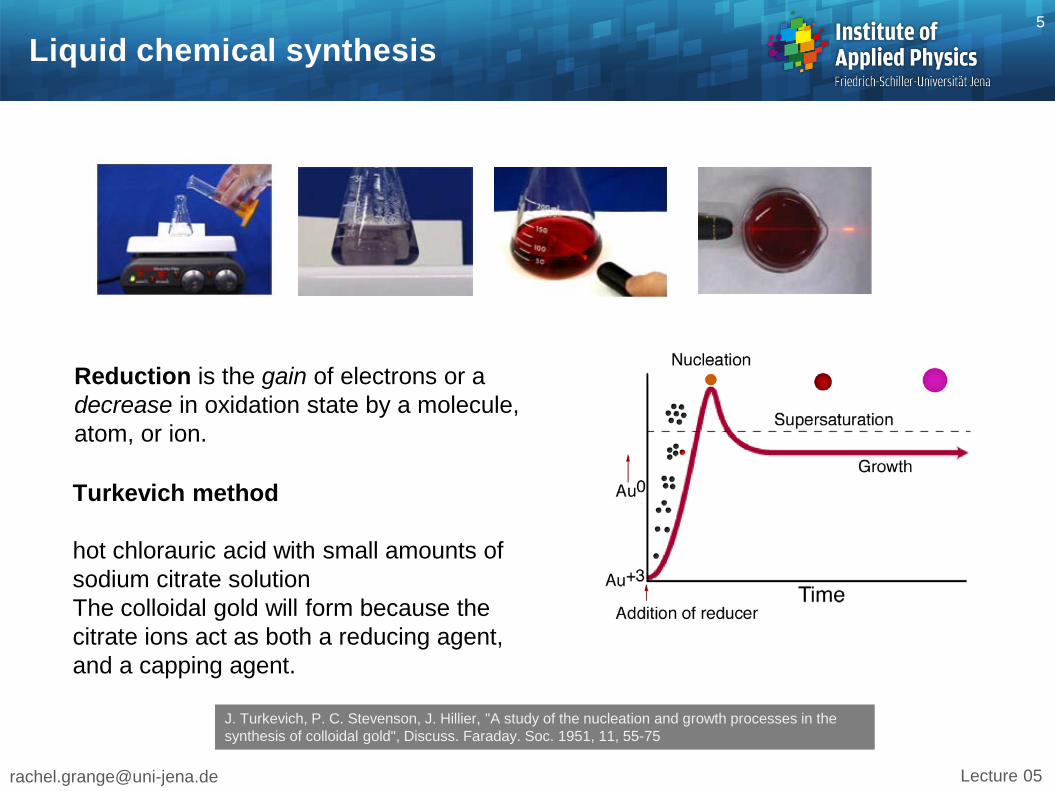
Reduction is the gain of electrons or a decrease in oxidation state by a molecule, atom, or ion.
Turkevich method hot chlorauric acid with small amounts of sodium citrate solution The colloidal gold will form because the citrate ions act as both a reducing agent, and a capping agent.
J. Turkevich, P. C. Stevenson, J. Hillier, "A study of the nucleation and growth processes in the synthesis of colloidal gold", Discuss. Faraday. Soc. 1951, 11, 55-75
[email protected] Lecture 05
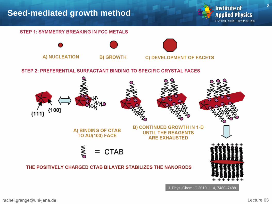
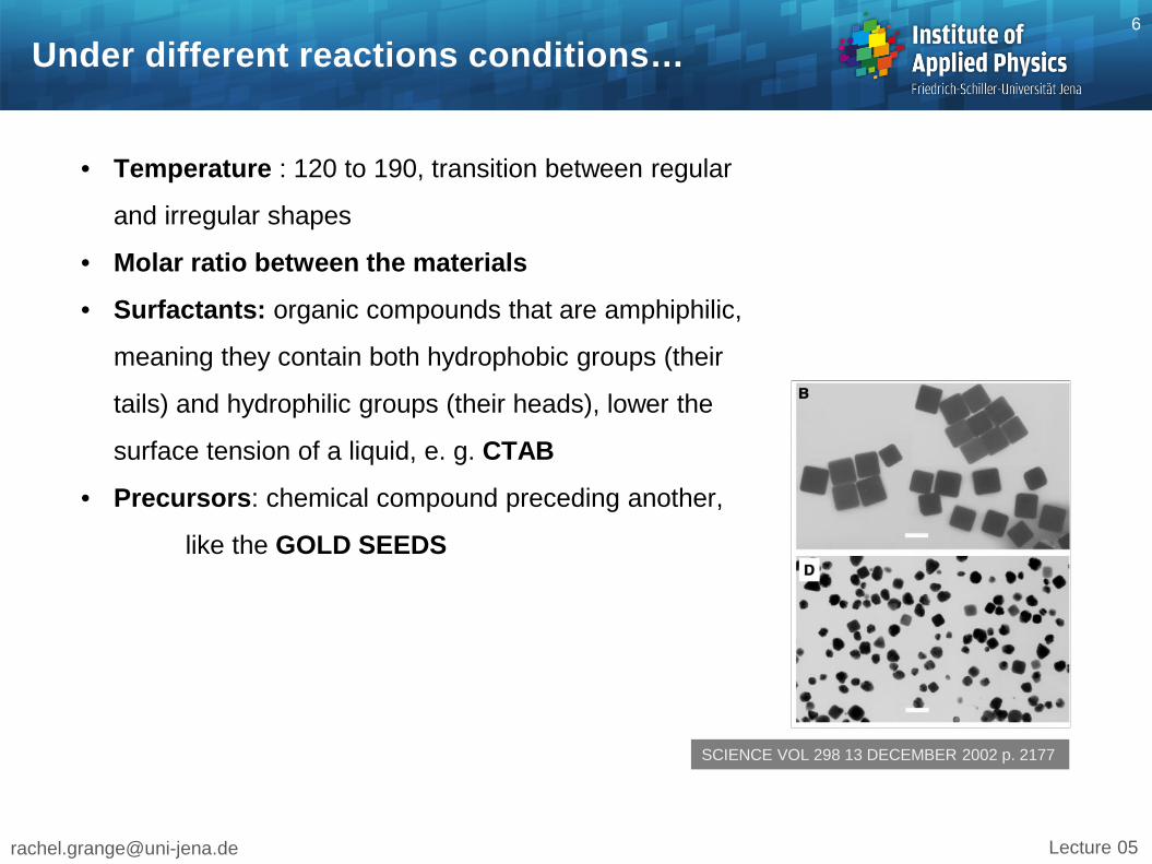
Under different reactions conditions… 6
• Temperature : 120 to 190, transition between regular
and irregular shapes
• Molar ratio between the materials
• Surfactants: organic compounds that are amphiphilic,
meaning they contain both hydrophobic groups (their
tails) and hydrophilic groups (their heads), lower the
surface tension of a liquid, e. g. CTAB
• Precursors: chemical compound preceding another,
like the GOLD SEEDS
SCIENCE VOL 298 13 DECEMBER 2002 p. 2177
[email protected] Lecture 05
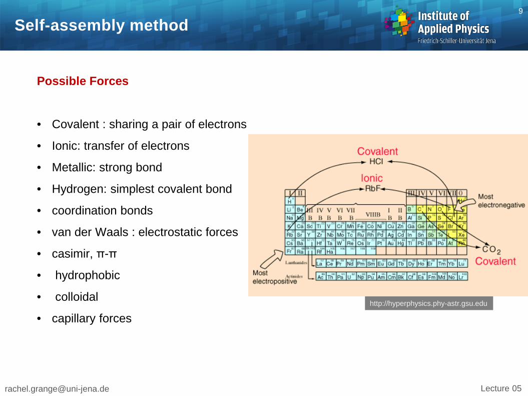
Self-assembly method 9
Possible Forces
• Covalent : sharing a pair of electrons
• Ionic: transfer of electrons
• Metallic: strong bond
• Hydrogen: simplest covalent bond
• coordination bonds
• van der Waals : electrostatic forces
• casimir, π-π
• hydrophobic
• colloidal
• capillary forces http://hyperphysics.phy-astr.gsu.edu
[email protected] Lecture 05
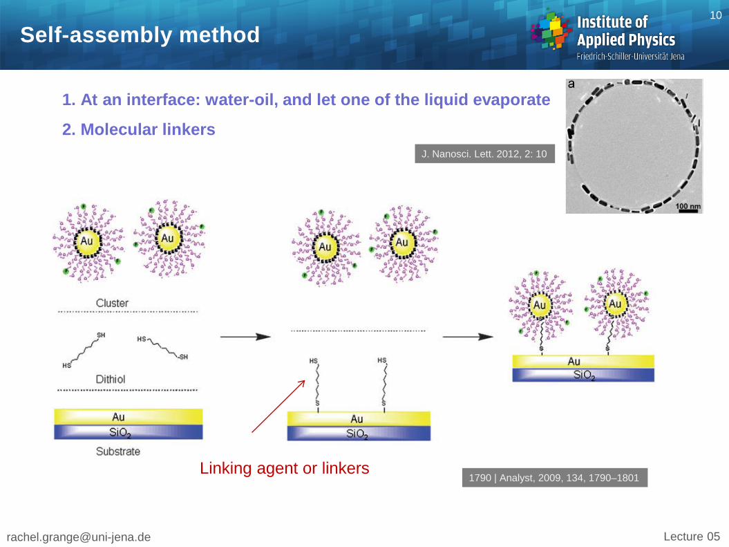
Self-assembly method 10
1790 | Analyst, 2009, 134, 1790–1801 Linking agent or linkers
1. At an interface: water-oil, and let one of the liquid evaporate
2. Molecular linkers J. Nanosci. Lett. 2012, 2: 10
[email protected] Lecture 05
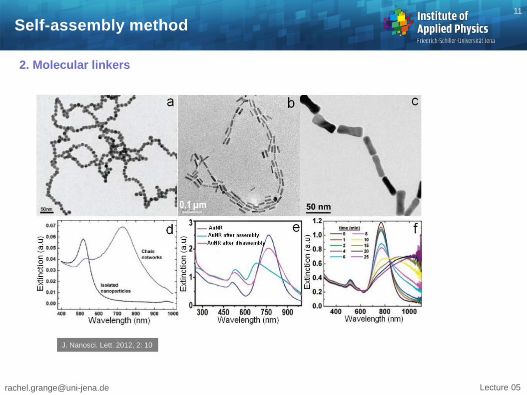
Self-assembly method 11
2. Molecular linkers
J. Nanosci. Lett. 2012, 2: 10
[email protected] Lecture 05
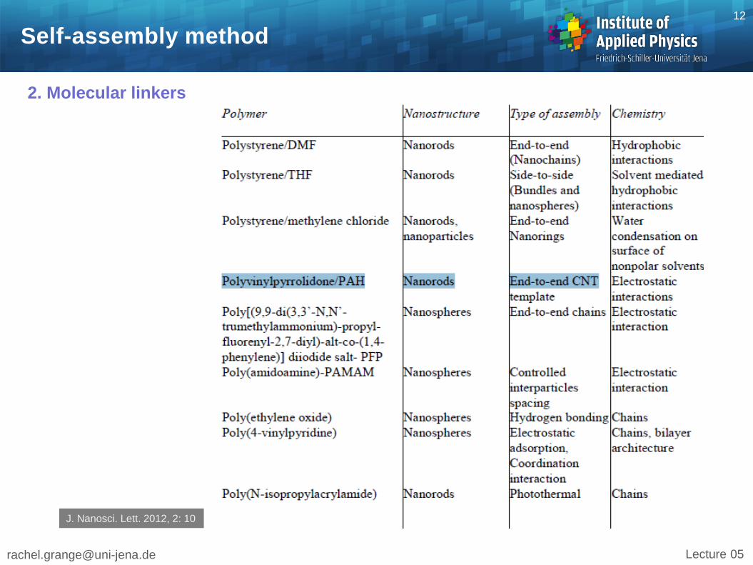
Self-assembly method 12
2. Molecular linkers
J. Nanosci. Lett. 2012, 2: 10
[email protected] Lecture 05
Self-assembly method 13
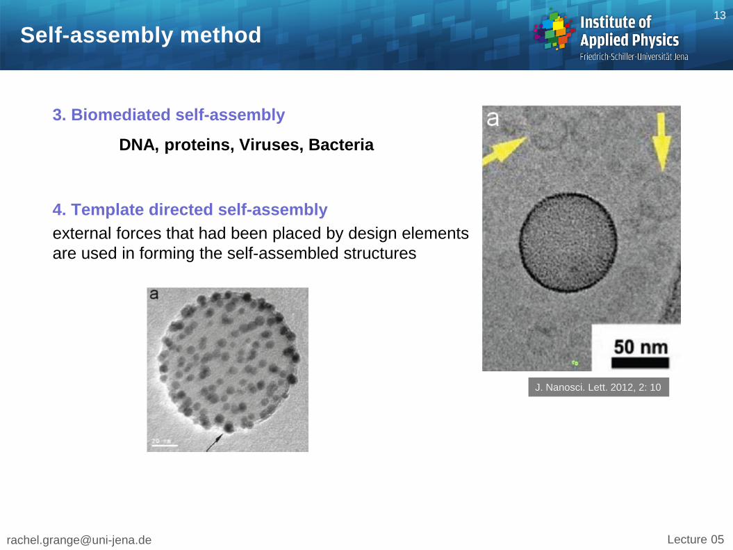
J. Nanosci. Lett. 2012, 2: 10
3. Biomediated self-assembly
DNA, proteins, Viruses, Bacteria
4. Template directed self-assembly external forces that had been placed by design elements are used in forming the self-assembled structures
[email protected] Lecture 05
Self-assembly method 14
ACS Nano, VOL. 4 ▪ NO. 7 ▪ 3591–3605 ▪ 2010
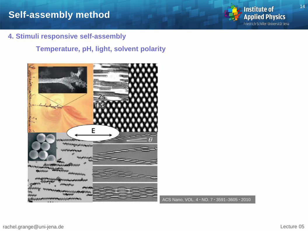
4. Stimuli responsive self-assembly
Temperature, pH, light, solvent polarity
[email protected] Lecture 05
Nanofabrication: Direct writing method 15
SCIENCE, p. 1407 VOL 332 17 JUNE 2011
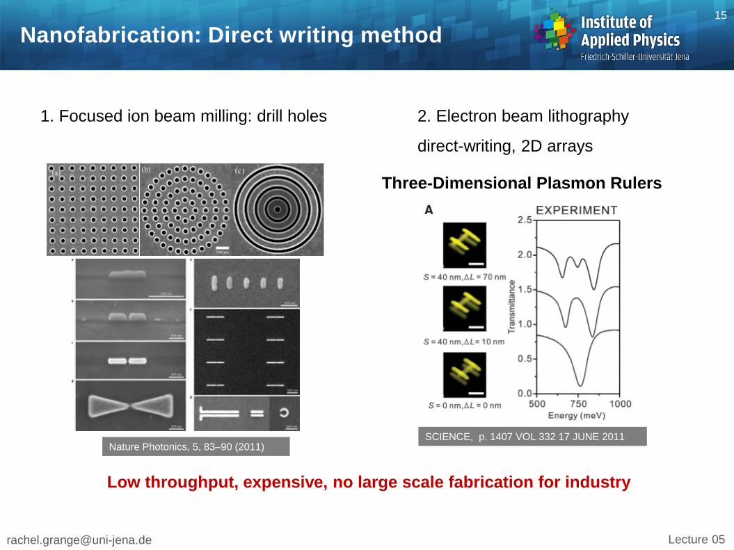
2. Electron beam lithography
direct-writing, 2D arrays
Three-Dimensional Plasmon Rulers
1. Focused ion beam milling: drill holes
Nature Photonics, 5, 83–90 (2011)
Low throughput, expensive, no large scale fabrication for industry
[email protected] Lecture 05
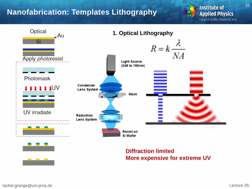
Nanofabrication: Templates Lithography 16
1. Optical Lithography
Diffraction limited More expensive for extreme UV
[email protected] Lecture 05
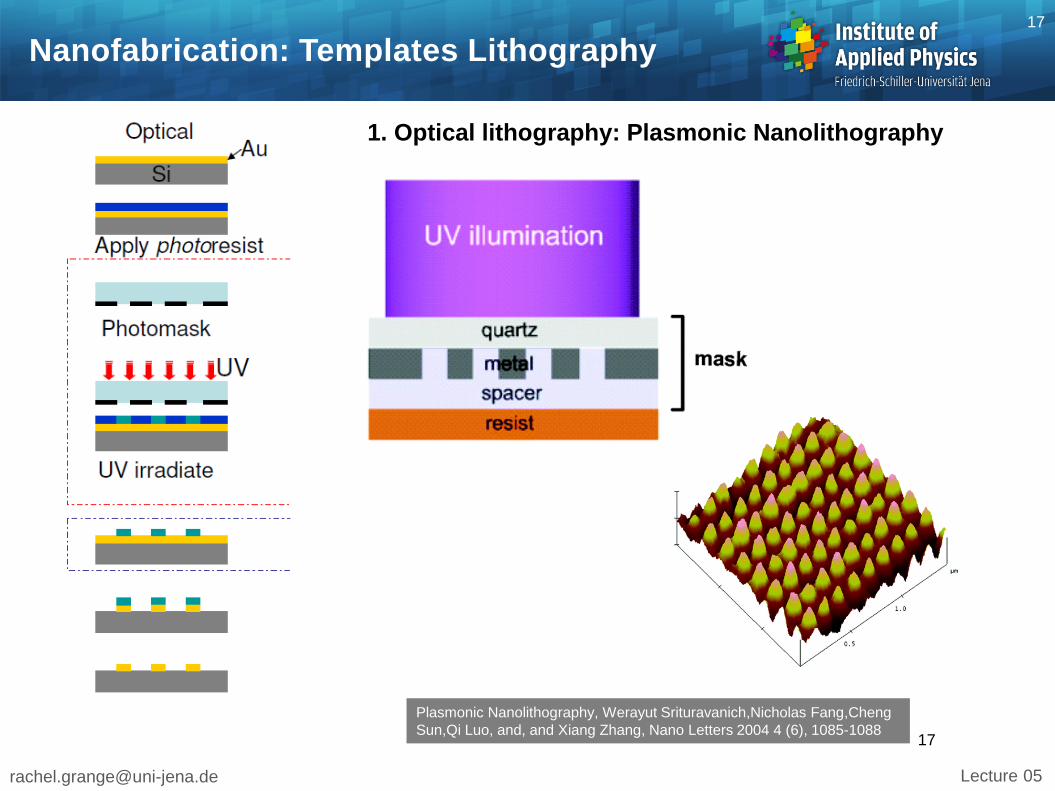
Nanofabrication: Templates Lithography 17
17
1. Optical lithography: Plasmonic Nanolithography
Plasmonic Nanolithography, Werayut Srituravanich,Nicholas Fang,Cheng Sun,Qi Luo, and, and Xiang Zhang, Nano Letters 2004 4 (6), 1085-1088
[email protected] Lecture 05
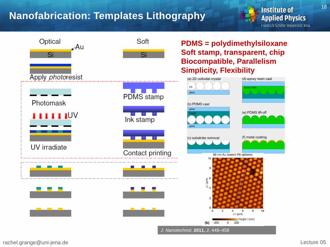
Nanofabrication: Templates Lithography 18
J. Nanotechnol. 2011, 2, 448–458
PDMS = polydimethylsiloxane Soft stamp, transparent, chip Biocompatible, Parallelism Simplicity, Flexibility
[email protected] Lecture 05
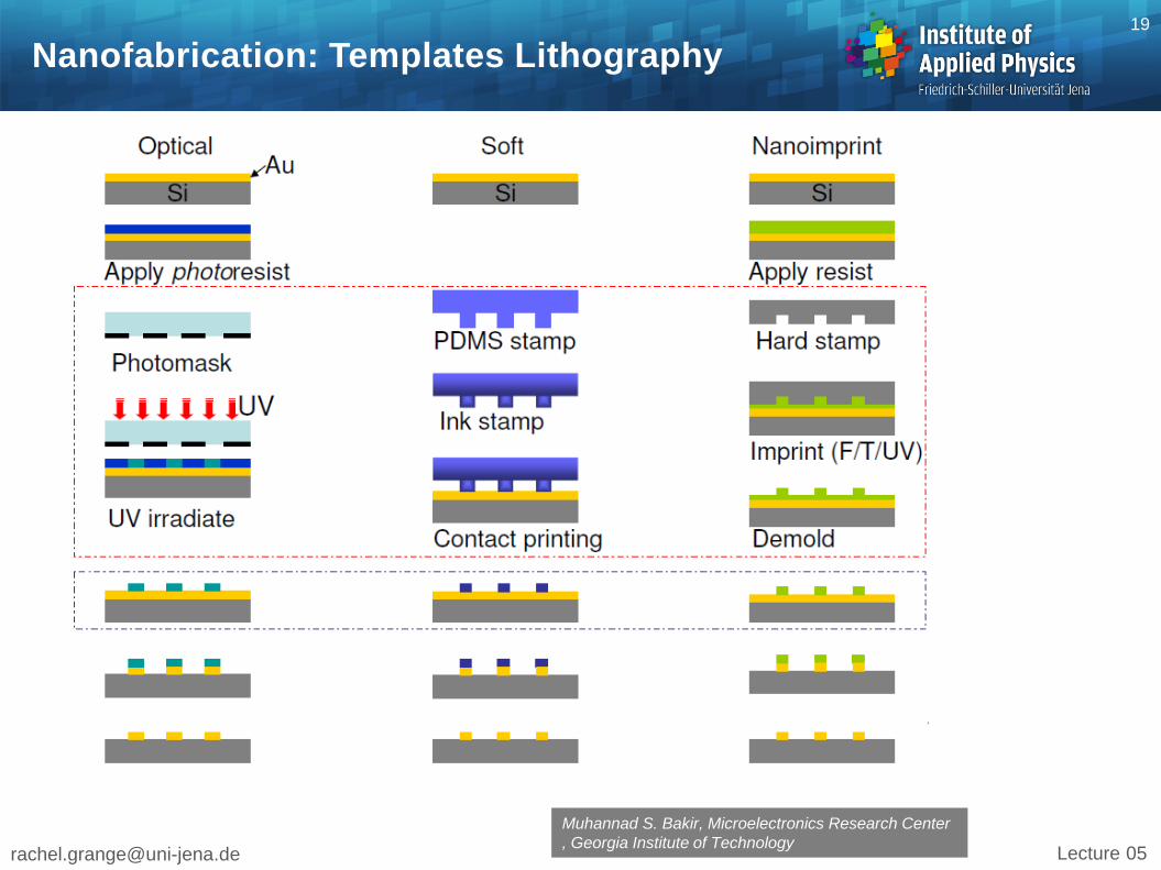
Nanofabrication: Templates Lithography 19
Muhannad S. Bakir, Microelectronics Research Center , Georgia Institute of Technology
[email protected] Lecture 05
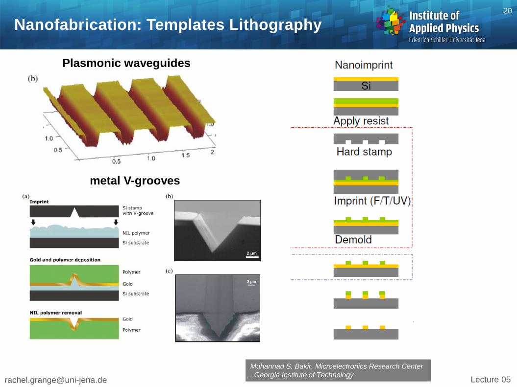
Nanofabrication: Templates Lithography 20
Muhannad S. Bakir, Microelectronics Research Center , Georgia Institute of Technology
metal V-grooves
Plasmonic waveguides
metal V-grooves
[email protected] Lecture 05
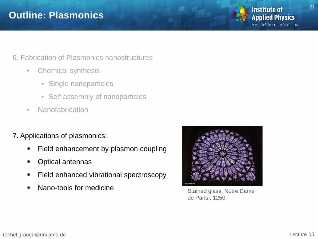
Outline: Plasmonics 21
6. Fabrication of Plasmonics nanostructures
• Chemical synthesis
• Single nanoparticles
• Self assembly of nanoparticles
• Nanofabrication
7. Applications of plasmonics:
Field enhancement by plasmon coupling
Optical antennas
Field enhanced vibrational spectroscopy
Nano-tools for medicine
Stained glass, Notre Dame de Paris , 1250
[email protected] Lecture 05
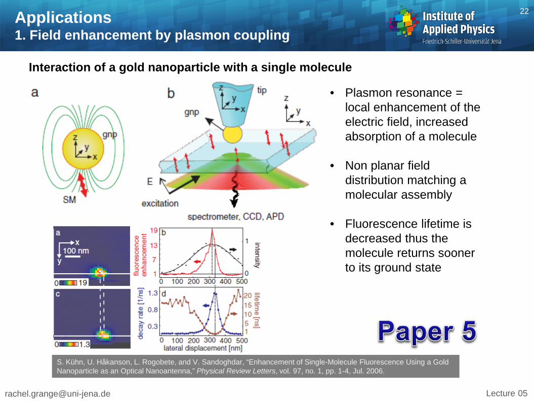
Applications 1. Field enhancement by plasmon coupling
22
S. Kühn, U. Håkanson, L. Rogobete, and V. Sandoghdar, “Enhancement of Single-Molecule Fluorescence Using a Gold Nanoparticle as an Optical Nanoantenna,” Physical Review Letters, vol. 97, no. 1, pp. 1-4, Jul. 2006.
• Plasmon resonance = local enhancement of the electric field, increased absorption of a molecule
• Non planar field distribution matching a molecular assembly
• Fluorescence lifetime is decreased thus the molecule returns sooner to its ground state
Interaction of a gold nanoparticle with a single molecule
[email protected] Lecture 05
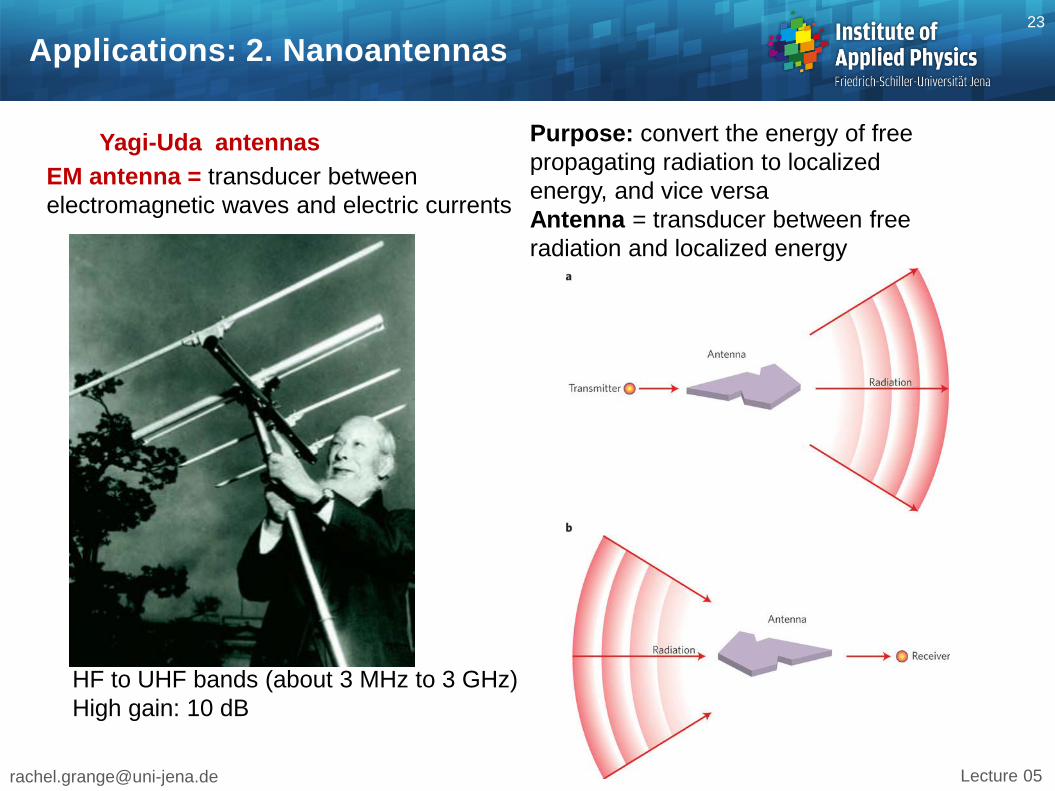
Applications: 2. Nanoantennas 23
Yagi-Uda antennas EM antenna = transducer between electromagnetic waves and electric currents
HF to UHF bands (about 3 MHz to 3 GHz) High gain: 10 dB
Purpose: convert the energy of free propagating radiation to localized energy, and vice versa Antenna = transducer between free radiation and localized energy
[email protected] Lecture 05
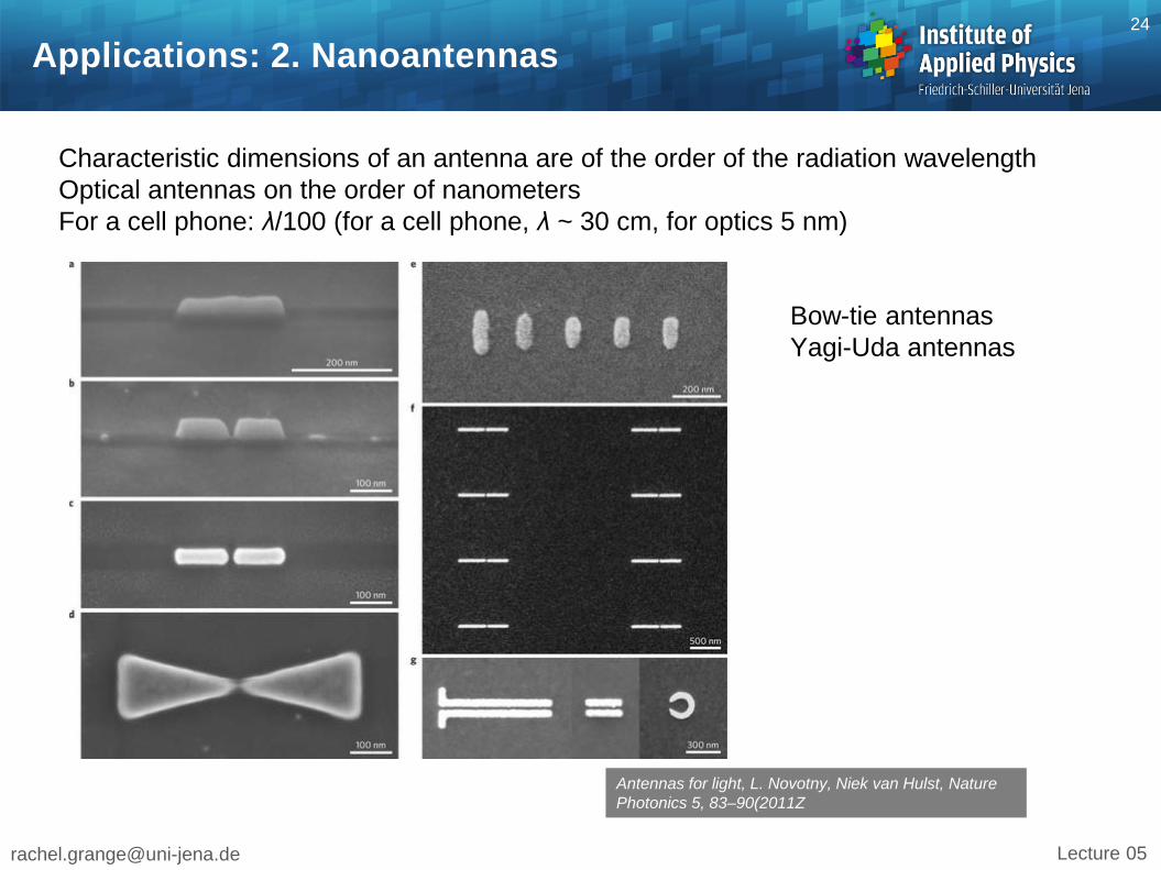
Applications: 2. Nanoantennas 24
Characteristic dimensions of an antenna are of the order of the radiation wavelength Optical antennas on the order of nanometers For a cell phone: λ/100 (for a cell phone, λ ~ 30 cm, for optics 5 nm)
Antennas for light, L. Novotny, Niek van Hulst, Nature Photonics 5, 83–90(2011Z
Bow-tie antennas Yagi-Uda antennas

[email protected] Lecture 05
Applications: 2. Nanoantennas 25
• all parts of the antennas are multiple or fraction of the em radiation λ
• Not at optical frequency: penetration of radiation into metals can no longer be neglected
Geometric constant Plasma wavelength
Metal not ideal (conductivity drops at the nanoscale) but carbon nanotubes or graphene
1. Photodetection and photovoltaics Increased absorption cross-section thus reduce the dimension, power consumption
2. Nanoimaging 3. Building blocks for data processing
[email protected] Lecture 05
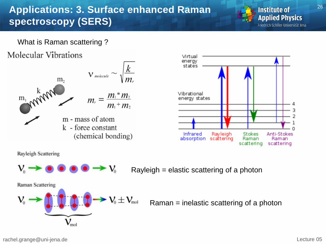
Applications: 3. Surface enhanced Raman spectroscopy (SERS)
26
What is Raman scattering ?
Raman = inelastic scattering of a photon
Rayleigh = elastic scattering of a photon
[email protected] Lecture 05
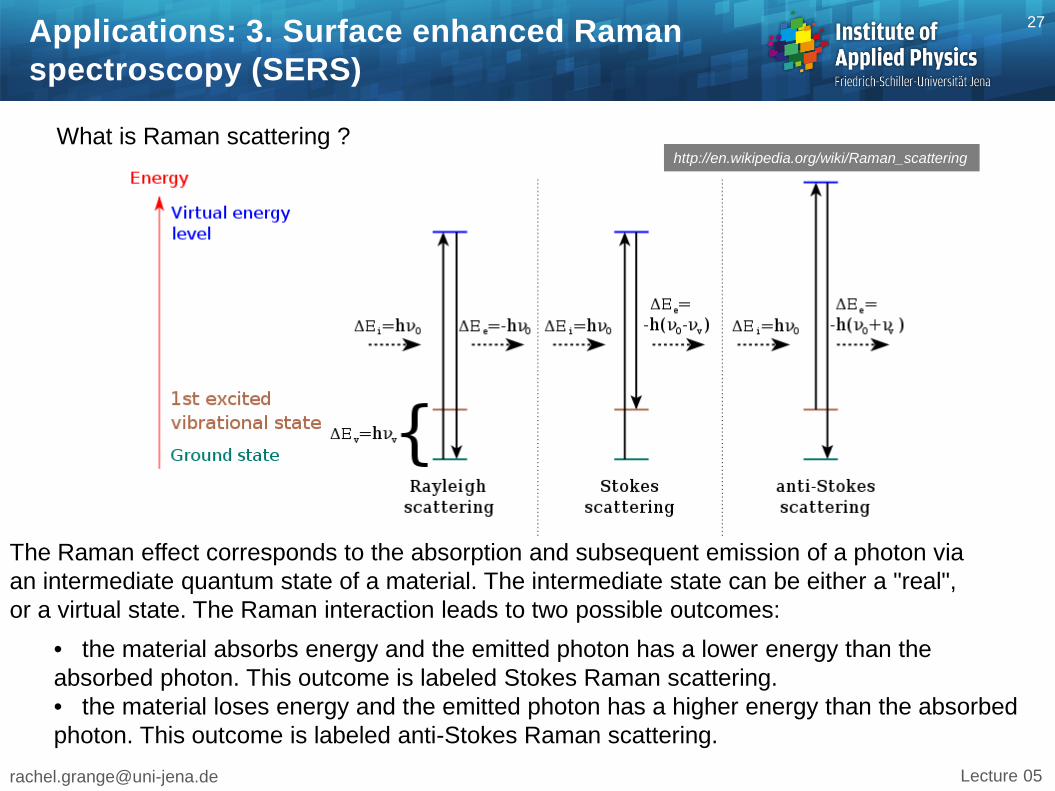
Applications: 3. Surface enhanced Raman spectroscopy (SERS)
27
What is Raman scattering ?
The Raman effect corresponds to the absorption and subsequent emission of a photon via an intermediate quantum state of a material. The intermediate state can be either a "real", or a virtual state. The Raman interaction leads to two possible outcomes:
• the material absorbs energy and the emitted photon has a lower energy than the absorbed photon. This outcome is labeled Stokes Raman scattering. • the material loses energy and the emitted photon has a higher energy than the absorbed photon. This outcome is labeled anti-Stokes Raman scattering.
http://en.wikipedia.org/wiki/Raman_scattering
[email protected] Lecture 05
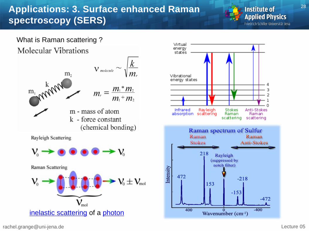
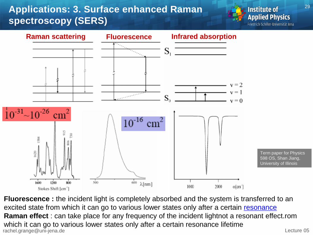
Applications: 3. Surface enhanced Raman spectroscopy (SERS)
28
What is Raman scattering ?
inelastic scattering of a photon
[email protected] Lecture 05
Applications: 3. Surface enhanced Raman spectroscopy (SERS)
29
Term paper for Physics 598 OS, Shan Jiang, University of Illinois
Raman scattering Fluorescence Infrared absorption
Fluorescence : the incident light is completely absorbed and the system is transferred to an excited state from which it can go to various lower states only after a certain resonance Raman effect : can take place for any frequency of the incident lightnot a resonant effect.rom which it can go to various lower states only after a certain resonance lifetime
[email protected] Lecture 05
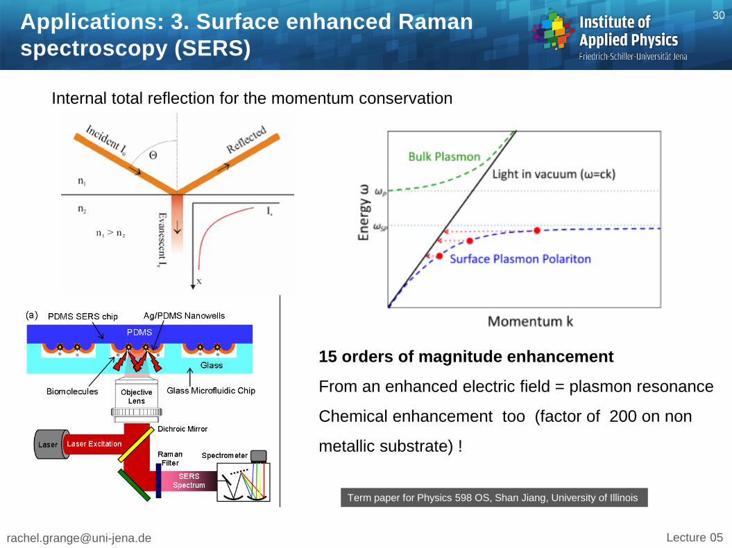
Applications: 3. Surface enhanced Raman spectroscopy (SERS)
30
Term paper for Physics 598 OS, Shan Jiang, University of Illinois
Internal total reflection for the momentum conservation
15 orders of magnitude enhancement
From an enhanced electric field = plasmon resonance
Chemical enhancement too (factor of 200 on non
metallic substrate) !

[email protected] Lecture 05
Applications: nanotools for medicine 31
Two combined effects: 1. Optical property: plasmon resonance 2. Thermal property : remaining energy HEAT
Metal particle = point-like sources of either light or heat
Heat generated in four different colloidal gold nanoparticles of same volume and fixed intensity
[email protected] Lecture 05
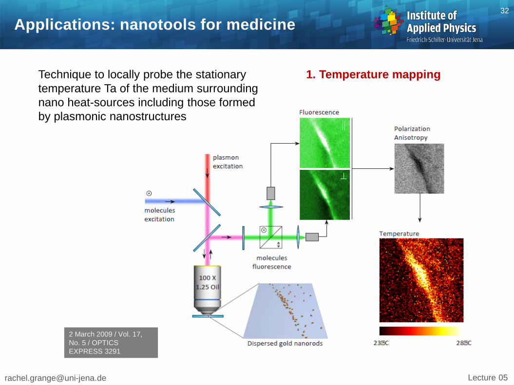
Applications: nanotools for medicine 32
1. Temperature mapping Technique to locally probe the stationary temperature Ta of the medium surrounding nano heat-sources including those formed by plasmonic nanostructures
2 March 2009 / Vol. 17, No. 5 / OPTICS EXPRESS 3291
[email protected] Lecture 05
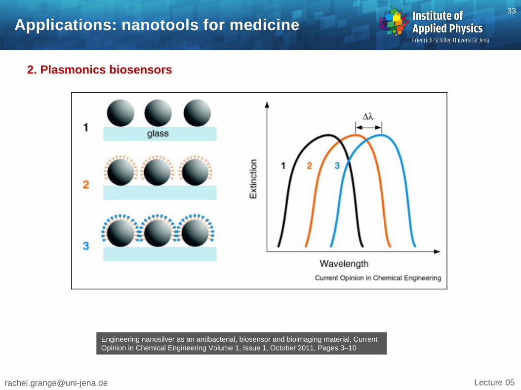
Applications: nanotools for medicine 33
2. Plasmonics biosensors
Engineering nanosilver as an antibacterial, biosensor and bioimaging material, Current Opinion in Chemical Engineering Volume 1, Issue 1, October 2011, Pages 3–10
[email protected] Lecture 05
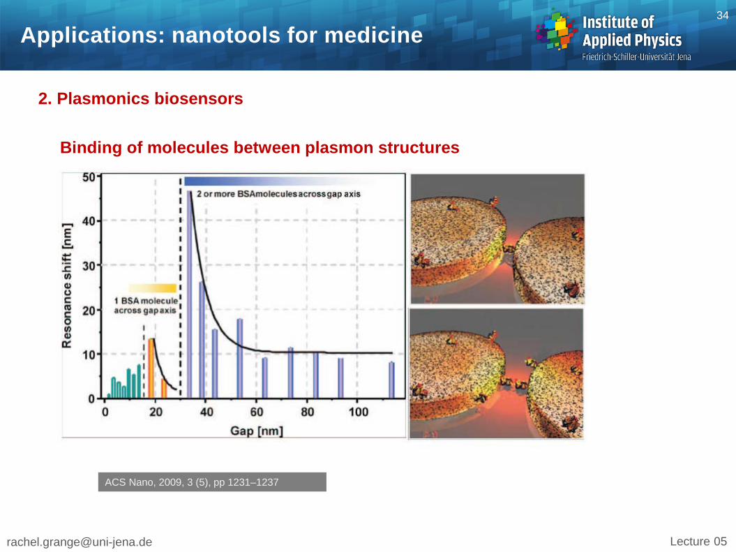
Applications: nanotools for medicine 34
2. Plasmonics biosensors
ACS Nano, 2009, 3 (5), pp 1231–1237
Binding of molecules between plasmon structures
[email protected] Lecture 05
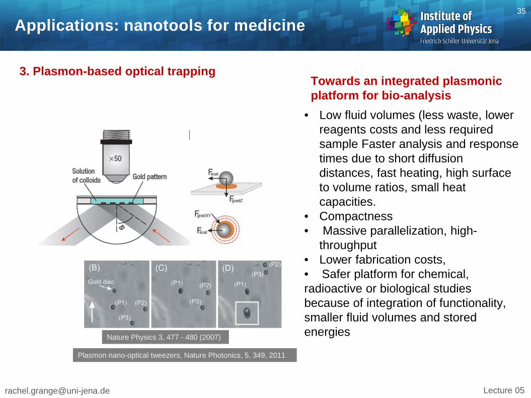
Applications: nanotools for medicine 35
3. Plasmon-based optical trapping
Nature Physics 3, 477 - 480 (2007)
Plasmon nano-optical tweezers, Nature Photonics, 5, 349, 2011
Towards an integrated plasmonic platform for bio-analysis
• Low fluid volumes (less waste, lower reagents costs and less required sample Faster analysis and response times due to short diffusion distances, fast heating, high surface to volume ratios, small heat capacities.
• Compactness • Massive parallelization, high-
throughput • Lower fabrication costs, • Safer platform for chemical, radioactive or biological studies because of integration of functionality, smaller fluid volumes and stored energies
[email protected] Lecture 05
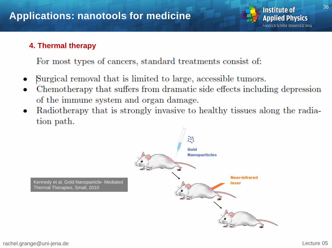
Applications: nanotools for medicine 36
4. Thermal therapy
Kennedy et al. Gold-Nanoparticle- Mediated Thermal Therapies, Small, 2010
[email protected] Lecture 05
Outlook 38
Plasmonics beyond the diffraction limit, Nature Photonics, 4, 83, 2010
S. Kühn, U. Håkanson, L. Rogobete, and V. Sandoghdar, “Enhancement of Single-Molecule Fluorescence Using a Gold Nanoparticle as an Optical Nanoantenna,” Physical Review Letters, vol. 97, no. 1, pp. 1-4, Jul. 2006.