This article was downloaded by: 10.3.98.104 On: 16 Feb 2022 Access details: subscription number Publisher: CRC Press Informa Ltd Registered in England and Wales Registered Number: 1072954 Registered office: 5 Howick Place, London SW1P 1WG, UK Nanomaterials Handbook Yury Gogotsi Epitaxial Graphene and Carbon Nanotubes on Silicon Carbide Publication details https://www.routledgehandbooks.com/doi/10.1201/9781315371795-3 Goknur Cambaz Büke Published online on: 22 Aug 2017 How to cite :- Goknur Cambaz Büke. 22 Aug 2017, Epitaxial Graphene and Carbon Nanotubes on Silicon Carbide from: Nanomaterials Handbook CRC Press Accessed on: 16 Feb 2022 https://www.routledgehandbooks.com/doi/10.1201/9781315371795-3 PLEASE SCROLL DOWN FOR DOCUMENT Full terms and conditions of use: https://www.routledgehandbooks.com/legal-notices/terms This Document PDF may be used for research, teaching and private study purposes. Any substantial or systematic reproductions, re-distribution, re-selling, loan or sub-licensing, systematic supply or distribution in any form to anyone is expressly forbidden. The publisher does not give any warranty express or implied or make any representation that the contents will be complete or accurate or up to date. The publisher shall not be liable for an loss, actions, claims, proceedings, demand or costs or damages whatsoever or howsoever caused arising directly or indirectly in connection with or arising out of the use of this material.
Transcript
This article was downloaded by: 10.3.98.104On: 16 Feb 2022Access details: subscription numberPublisher: CRC PressInforma Ltd Registered in England and Wales Registered Number: 1072954 Registered office: 5 Howick Place, London SW1P 1WG, UK
Nanomaterials Handbook
Yury Gogotsi
Epitaxial Graphene and Carbon Nanotubes on SiliconCarbide
Goknur Cambaz BükePublished online on: 22 Aug 2017
How to cite :- Goknur Cambaz Büke. 22 Aug 2017, Epitaxial Graphene and Carbon Nanotubes onSilicon Carbide from: Nanomaterials Handbook CRC PressAccessed on: 16 Feb 2022https://www.routledgehandbooks.com/doi/10.1201/9781315371795-3
PLEASE SCROLL DOWN FOR DOCUMENT
Full terms and conditions of use: https://www.routledgehandbooks.com/legal-notices/terms
This Document PDF may be used for research, teaching and private study purposes. Any substantial or systematic reproductions,re-distribution, re-selling, loan or sub-licensing, systematic supply or distribution in any form to anyone is expressly forbidden.
The publisher does not give any warranty express or implied or make any representation that the contents will be complete oraccurate or up to date. The publisher shall not be liable for an loss, actions, claims, proceedings, demand or costs or damageswhatsoever or howsoever caused arising directly or indirectly in connection with or arising out of the use of this material.
Dow
nloa
ded
By:
10.
3.98
.104
At:
22:3
6 16
Feb
202
2; F
or: 9
7813
1537
1795
, cha
pter
3, 1
0.12
01/9
7813
1537
1795
-3
63
Epitaxial Graphene and Carbon Nanotubes on Silicon Carbide
Goknur Cambaz Büke
3.1 EPITAXIAL GRAPHENE AND CNTs ON SiC
Graphene (i.e., a single layer of graphite) and carbon nanotubes (CNTs; i.e., graphene rolled into a cylinder) are excellent candidate materials for advanced applications because of their unique electri-cal, optical, and mechanical properties combined with a high surface area. The successful develop-ment of graphene-/CNT-based technology depends on large-scale availability of the high-quality, reproducible, and uniformly ordered material. One of the most versatile methods to produce verti-cally, self-aligned CNTs and epitaxial graphene is the vacuum annealing of silicon carbide single crystals [1,2]. This is a very versatile method because carbon is supplied from the carbide lattice as known from the synthesis of carbide-derived carbons (CDCs, see Figure 3.1) and, as no catalysts or secondary phases are utilized; the produced graphene and CNTs exhibit extremely high purity. However, to increase the grain/domain size and quality of these carbon nanostructures, further control of the process is needed.
Understanding the effects of experimental parameters of the processes is the basis for tailor-ing the resulting material so as to enable applications. Therefore, this chapter describes the factors (as summarized in Figure 3.2) influencing the vacuum-annealing process of SiC and the reaction mechanisms.
3.1.1 History on tHermal Decomposition of sic
Initially, studying thermal decomposition of solids was for the purpose of examining thermal stabil-ity of materials. With the discovery of epitaxial growth of graphene and self-aligned CNTs on the crystal surfaces of silicon carbide, thermal decomposition has developed into a facile method of producing catalyst-free, high-purity, and highly homogeneous carbon.
3
CONTENTS
3.1 Epitaxial Graphene and CNTs on SiC .................................................................................... 633.1.1 History on Thermal Decomposition of SiC ................................................................ 633.1.2 Factors Affecting the Carbon Growth on SiC ............................................................65
3.1.2.1 SiC Polytypism ............................................................................................653.1.2.2 SiC Material Type ........................................................................................ 673.1.2.3 SiC Substrate Surface Morphology .............................................................693.1.2.4 Growth Conditions ....................................................................................... 73
3.1.3 CNT and Graphene-Formation Mechanism on SiC ................................................... 783.2 Summary ................................................................................................................................ 79Acknowledgment ............................................................................................................................. 79References ........................................................................................................................................ 79
Dow
nloa
ded
By:
10.
3.98
.104
At:
22:3
6 16
Feb
202
2; F
or: 9
7813
1537
1795
, cha
pter
3, 1
0.12
01/9
7813
1537
1795
-364 Nanomaterials Handbook
(a) (d)
5 nm
1700°C, C face
1700°C, Si face
(e)
50 nm
5 nm
1250°C
1300°C
1350°C
(c)
C face
C face
Si face
5 nm
(b)
FIGURE 3.2 Cross-sectional HRTEM images showing surfaces of the C face heated at (a) 1250°C, (b) 1300°C, (c) the Si face heated at 1350°C for half an hour, (d) C face, and (e) Si face heated at 1700°C for half an hour. Inset in (d) shows the CNT film observed along a CNT axis plane–view direction. (Adapted and modified from Kusunoki, M. et al., Philosophical Magazine Letters, 1999. 79(4): 153–161; Kusunoki, M. et al., Applied Physics Letters, 2000. 77(4): 531–533.)
Si sublimation
C face ( :C)
As-received 6H-SiC
High temperature
10–6 Torr, 1700–1900°CSiC Vacuum
C(s) + Si(g)
Si face ( Si)
Self-organization of surfacecarbon atoms intoCNT or graphene
FIGURE 3.1 Schematic drawing of the formation of SiC-derived carbon resulting in layers of CNT and graphene.
Dow
nloa
ded
By:
10.
3.98
.104
At:
22:3
6 16
Feb
202
2; F
or: 9
7813
1537
1795
, cha
pter
3, 1
0.12
01/9
7813
1537
1795
-365Epitaxial Graphene and Carbon Nanotubes on Silicon Carbide
The first documented observation of carbon formation by vacuum annealing of SiC was published in 1962 (employing temperatures up to 2150°C) [3]. A decade later, Bommel et al. [4] found mono-layers of graphite on SiC after annealing at 800°C and enhanced graphitization around 1500°C. Later, in the 1980s and 1990s, the work of Bommel was confirmed by Muehlhoff et al. [5], Forbeaux et al. [6], and Charrier et al. [7] who reported similar results. However, graphitic structures were not the only structures reported. A new interest in the thermal decomposition of SiC arose in 1997 when Kusunoki et al. [8] discovered the growth of self-organized carbon nanotube films by heating SiC wafer at 1700°C for half an hour in a vacuum furnace (P = 1 × 10⁻⁴ Torr) [9]. Later, a model was proposed for the formation mechanism of the CNT film on SiC that consisted of three stages. At temperatures above 1000°C (stage I), several graphene sheets were formed parallel to the (0001) SiC plane. At around ≈1300°C (stage II), carbon nanocaps grow. At stage III, the graphite sheets align upward and CNTs grow toward the interior of the SiC crystal.
Further investigations were carried out on both the Si- and C-terminated basal plane of hex-agonal silicon carbide faces by using cross-sectional high-resolution transmission electron micros-copy (HRTEM) at lower temperatures [10]. A remarkable difference between the carbon structures formed on (0001)Si and ( )0001 C-faces of a 6H-SiC single crystals was shown. Although CNT growth was observed under various experimental conditions on the C-face, only flat graphite sheets parallel to the surface were found to be stable on the Si-face (Figure 3.2).
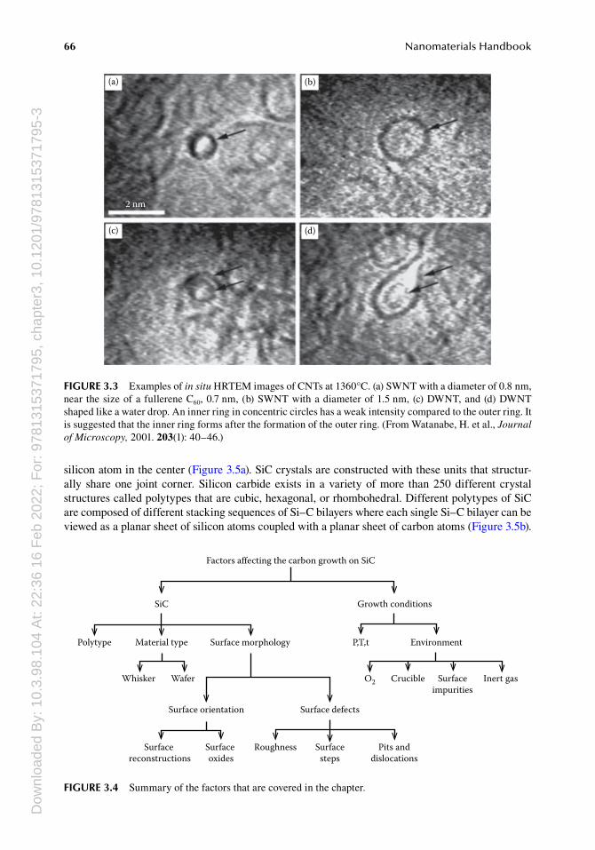
To study the initial growth process of CNTs at lower temperatures (≈1300°C), Watanabe et al. [11] observed the in situ formation of CNTs on β-SiC (111) single crystal inside a TEM and pro-posed that the caps of the CNTs were formed by a lift of a part of the graphene through the gen-eration of pentagons and heptagons. It was confirmed that around 1360°C amorphous carbon with many holes and defects forms because of the desorption of Si atoms. Afterward, these carbon layers crystallize into graphitic layers. Successive heating at the appropriate temperature results in two types of CNTs: single-walled carbon nanotubes (SWCNTs) with a diameter of 0.8 and 1.5 nm and double-walled carbon nanotubes (DWCNTs; Figure 3.3). It was confirmed by scanning tunneling microscopy (STM) measurements that the ends of the CNTs were closed (capped).
However, these studies did not explain why different carbon structures occur on Si and C faces and why the results provided by different research groups differed so greatly. In 2004, the paral-lel publication of the electrical response of graphene by Novoselov et al. [12] and Berger et al. [13] provided new motivation to optimize the growth conditions of graphene on SiC that required a deep understanding of the processes involved at the atomic level during decomposition.
3.1.2 factors affecting tHe carbon growtH on sic
The reactions that take place when SiC is heated can be summarized as follows:
1. SiC surface reconstruction and surface-oxide removal 2. SiC decomposition: breaking of Si–C bonds (SiC → C(s) + Si(g)) 3. Si desorption 4. C diffusion on the surface (self-organization of carbon atoms into carbon nanostructures)
that results in carbon islands/graphene nucleation 5. Growth of the nucleus
The nucleation and growth of graphene/CNT are highly dependent on SiC surface morphology and the general growth conditions [14] (as summarized in Figure 3.4), which are outlined in more detail in the following sections.
3.1.2.1 SiC PolytypismThe morphology of epitaxial graphene/CNT is highly influenced by the underlying SiC structure. The basic building block of a silicon carbide is a tetrahedron with four carbon atoms and a single
Dow
nloa
ded
By:
10.
3.98
.104
At:
22:3
6 16
Feb
202
2; F
or: 9
7813
1537
1795
, cha
pter
3, 1
0.12
01/9
7813
1537
1795
-366 Nanomaterials Handbook
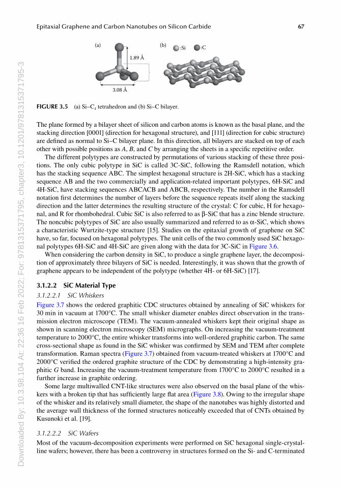
silicon atom in the center (Figure 3.5a). SiC crystals are constructed with these units that structur-ally share one joint corner. Silicon carbide exists in a variety of more than 250 different crystal structures called polytypes that are cubic, hexagonal, or rhombohedral. Different polytypes of SiC are composed of different stacking sequences of Si–C bilayers where each single Si–C bilayer can be viewed as a planar sheet of silicon atoms coupled with a planar sheet of carbon atoms (Figure 3.5b).
Factors affecting the carbon growth on SiC
SiC Growth conditions
P,T,t Environment
Crucible Surfaceimpurities
O2
Polytype Material type Surface morphology
Surface orientation
Surface reconstructions
Surface oxides
Roughness Surfacesteps
Pits anddislocations
Surface defects
Whisker Wafer Inert gas
FIGURE 3.4 Summary of the factors that are covered in the chapter.
(a)
2 nm
(c) (d)
(b)
FIGURE 3.3 Examples of in situ HRTEM images of CNTs at 1360°C. (a) SWNT with a diameter of 0.8 nm, near the size of a fullerene C60, 0.7 nm, (b) SWNT with a diameter of 1.5 nm, (c) DWNT, and (d) DWNT shaped like a water drop. An inner ring in concentric circles has a weak intensity compared to the outer ring. It is suggested that the inner ring forms after the formation of the outer ring. (From Watanabe, H. et al., Journal of Microscopy, 2001. 203(1): 40–46.)
Dow
nloa
ded
By:
10.
3.98
.104
At:
22:3
6 16
Feb
202
2; F
or: 9
7813
1537
1795
, cha
pter
3, 1
0.12
01/9
7813
1537
1795
-367Epitaxial Graphene and Carbon Nanotubes on Silicon Carbide
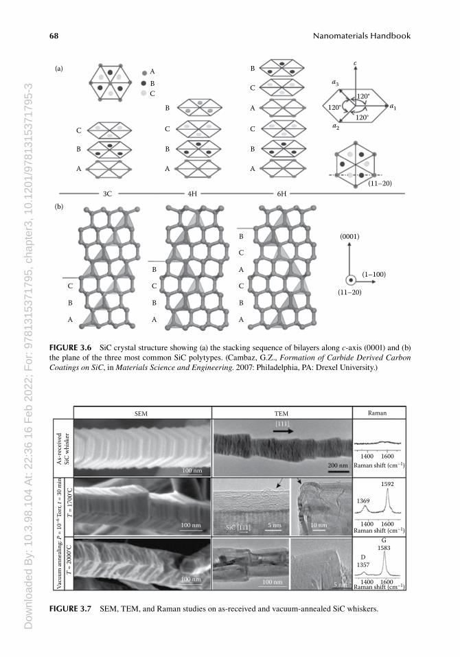
The plane formed by a bilayer sheet of silicon and carbon atoms is known as the basal plane, and the stacking direction [0001] (direction for hexagonal structure), and [111] (direction for cubic structure) are defined as normal to Si–C bilayer plane. In this direction, all bilayers are stacked on top of each other with possible positions as A, B, and C by arranging the sheets in a specific repetitive order.
The different polytypes are constructed by permutations of various stacking of these three posi-tions. The only cubic polytype in SiC is called 3C-SiC, following the Ramsdell notation, which has the stacking sequence ABC. The simplest hexagonal structure is 2H-SiC, which has a stacking sequence AB and the two commercially and application-related important polytypes, 6H-SiC and 4H-SiC, have stacking sequences ABCACB and ABCB, respectively. The number in the Ramsdell notation first determines the number of layers before the sequence repeats itself along the stacking direction and the latter determines the resulting structure of the crystal: C for cubic, H for hexago-nal, and R for rhombohedral. Cubic SiC is also referred to as β-SiC that has a zinc blende structure. The noncubic polytypes of SiC are also usually summarized and referred to as α-SiC, which shows a characteristic Wurtzite-type structure [15]. Studies on the epitaxial growth of graphene on SiC have, so far, focused on hexagonal polytypes. The unit cells of the two commonly used SiC hexago-nal polytypes 6H-SiC and 4H-SiC are given along with the data for 3C-SiC in Figure 3.6.
When considering the carbon density in SiC, to produce a single graphene layer, the decomposi-tion of approximately three bilayers of SiC is needed. Interestingly, it was shown that the growth of graphene appears to be independent of the polytype (whether 4H- or 6H-SiC) [17].
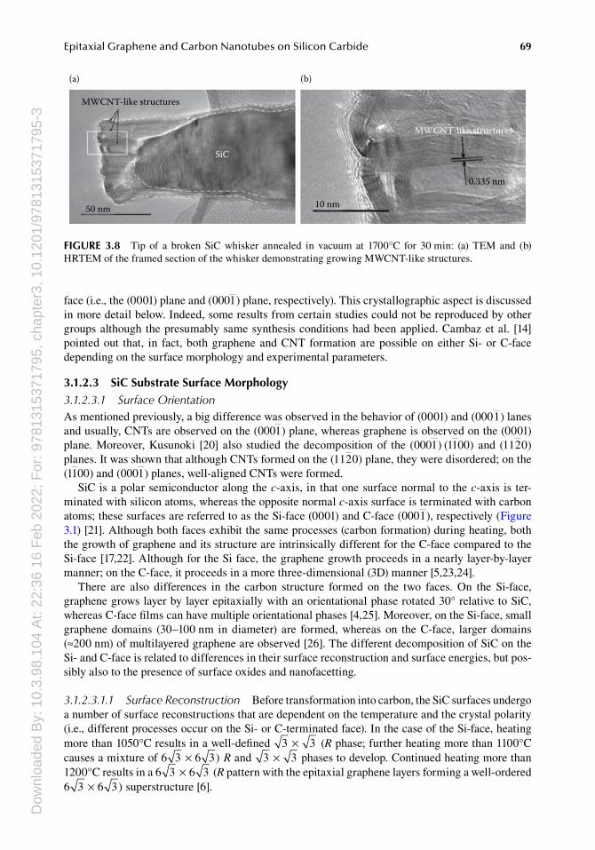
3.1.2.2 SiC Material Type3.1.2.2.1 SiC WhiskersFigure 3.7 shows the ordered graphitic CDC structures obtained by annealing of SiC whiskers for 30 min in vacuum at 1700°C. The small whisker diameter enables direct observation in the trans-mission electron microscope (TEM). The vacuum-annealed whiskers kept their original shape as shown in scanning electron microscopy (SEM) micrographs. On increasing the vacuum-treatment temperature to 2000°C, the entire whisker transforms into well-ordered graphitic carbon. The same cross-sectional shape as found in the SiC whisker was confirmed by SEM and TEM after complete transformation. Raman spectra (Figure 3.7) obtained from vacuum-treated whiskers at 1700°C and 2000°C verified the ordered graphite structure of the CDC by demonstrating a high-intensity gra-phitic G band. Increasing the vacuum-treatment temperature from 1700°C to 2000°C resulted in a further increase in graphite ordering.
Some large multiwalled CNT-like structures were also observed on the basal plane of the whis-kers with a broken tip that has sufficiently large flat area (Figure 3.8). Owing to the irregular shape of the whisker and its relatively small diameter, the shape of the nanotubes was highly distorted and the average wall thickness of the formed structures noticeably exceeded that of CNTs obtained by Kusunoki et al. [19].
3.1.2.2.2 SiC WafersMost of the vacuum-decomposition experiments were performed on SiC hexagonal single-crystal-line wafers; however, there has been a controversy in structures formed on the Si- and C-terminated
1.89 Å
(b) :Si :C(a)
3.08 Å
FIGURE 3.5 (a) Si–C4 tetrahedron and (b) Si–C bilayer.
Dow
nloa
ded
By:
10.
3.98
.104
At:
22:3
6 16
Feb
202
2; F
or: 9
7813
1537
1795
, cha
pter
3, 1
0.12
01/9
7813
1537
1795
-368 Nanomaterials Handbook
(a)
(b)
ABC
C
B
B
C
B
A A
B
C
A
C
Bc
a3
a1
a2
A
A
B
C
B
C C
C
B
B B
A A
A
3C 4H 6H
120°120°
120°
(11–20)
(0001)
(11–20)
(1–100)
FIGURE 3.6 SiC crystal structure showing (a) the stacking sequence of bilayers along c-axis (0001) and (b) the plane of the three most common SiC polytypes. (Cambaz, G.Z., Formation of Carbide Derived Carbon Coatings on SiC, in Materials Science and Engineering. 2007: Philadelphia, PA: Drexel University.)
SEM
As-
rece
ived
SiC
whi
sker
Vacu
um an
neal
ing:
P =
10–6
Tor
r, t =
30
min
T =
1700
°CT
= 20
00°C
100 nm
100 nm
100 nm 100 nm
SiC [111] 5 nm 10 nm
5 nm
200 nm
TEM[111]
Raman
1400 1600
1400
D1357
G1583
1369
1592
1600
Raman shift (cm–1)
Raman shift (cm–1)
1400 1600Raman shift (cm–1)
FIGURE 3.7 SEM, TEM, and Raman studies on as-received and vacuum-annealed SiC whiskers.
Dow
nloa
ded
By:
10.
3.98
.104
At:
22:3
6 16
Feb
202
2; F
or: 9
7813
1537
1795
, cha
pter
3, 1
0.12
01/9
7813
1537
1795
-369Epitaxial Graphene and Carbon Nanotubes on Silicon Carbide
face (i.e., the (0001) plane and ( )0001 plane, respectively). This crystallographic aspect is discussed in more detail below. Indeed, some results from certain studies could not be reproduced by other groups although the presumably same synthesis conditions had been applied. Cambaz et al. [14] pointed out that, in fact, both graphene and CNT formation are possible on either Si- or C-face depending on the surface morphology and experimental parameters.
3.1.2.3 SiC Substrate Surface Morphology3.1.2.3.1 Surface OrientationAs mentioned previously, a big difference was observed in the behavior of (0001) and ( )0001 lanes and usually, CNTs are observed on the ( )0001 plane, whereas graphene is observed on the (0001) plane. Moreover, Kusunoki [20] also studied the decomposition of the ( ) ( )0001 1100 and ( )11 02 planes. It was shown that although CNTs formed on the ( )11 02 plane, they were disordered; on the ( )1100 and ( )0001 planes, well-aligned CNTs were formed.
SiC is a polar semiconductor along the c-axis, in that one surface normal to the c-axis is ter-minated with silicon atoms, whereas the opposite normal c-axis surface is terminated with carbon atoms; these surfaces are referred to as the Si-face (0001) and C-face ( ),0001 respectively (Figure 3.1) [21]. Although both faces exhibit the same processes (carbon formation) during heating, both the growth of graphene and its structure are intrinsically different for the C-face compared to the Si-face [17,22]. Although for the Si face, the graphene growth proceeds in a nearly layer-by-layer manner; on the C-face, it proceeds in a more three-dimensional (3D) manner [5,23,24].
There are also differences in the carbon structure formed on the two faces. On the Si-face, graphene grows layer by layer epitaxially with an orientational phase rotated 30° relative to SiC, whereas C-face films can have multiple orientational phases [4,25]. Moreover, on the Si-face, small graphene domains (30–100 nm in diameter) are formed, whereas on the C-face, larger domains (≈200 nm) of multilayered graphene are observed [26]. The different decomposition of SiC on the Si- and C-face is related to differences in their surface reconstruction and surface energies, but pos-sibly also to the presence of surface oxides and nanofacetting.
3.1.2.3.1.1 Surface Reconstruction Before transformation into carbon, the SiC surfaces undergo a number of surface reconstructions that are dependent on the temperature and the crystal polarity (i.e., different processes occur on the Si- or C-terminated face). In the case of the Si-face, heating more than 1050°C results in a well-defined 3 3× (R phase; further heating more than 1100°C causes a mixture of 6 3 6 3× ) R and 3 3× phases to develop. Continued heating more than 1200°C results in a 6 3 6 3× (R pattern with the epitaxial graphene layers forming a well-ordered 6 3 6 3× ) superstructure [6].
MWCNT-like structures
(a) (b)
MWCNT-like structures
0.335 nm
SiC
50 nm 10 nm
FIGURE 3.8 Tip of a broken SiC whisker annealed in vacuum at 1700°C for 30 min: (a) TEM and (b) HRTEM of the framed section of the whisker demonstrating growing MWCNT-like structures.
Dow
nloa
ded
By:
10.
3.98
.104
At:
22:3
6 16
Feb
202
2; F
or: 9
7813
1537
1795
, cha
pter
3, 1
0.12
01/9
7813
1537
1795
-370 Nanomaterials Handbook
On the C-face, heating SiC results in several different reconstructions: heating at 1050°C for 15 min removes the native oxide layer and gives a (3 × 3) reconstruction [27,28]. Continued heating at 1075°C produces a (2 × 2) C phase in coexistence with the (3 × 3) phase [29]. Graphene grown on the C-face is much more randomly oriented that is indicative of a much weaker substrate influence [26].
3.1.2.3.1.2 Surface Oxides The oxide layers on C- and Si-terminated faces of SiC differ in composition and structure [27,30]. The oxide layer is directly connected to the topmost SiC bilayer by a Si–C bond on ( )0001 whereas a linear Si–O–Si bridge makes the contact on (0001). The lat-ter structure leads to a stronger bonding and a slower decomposition rate of the Si-face. Zinovev et al. [31] observed a thicker oxide layer on the Si-face compared to the C-face. X-ray photoelectron spectroscopy (XPS) analysis of SiC wafers detected SiOxCy on the C-face and Si-face; however, the oxygen content was higher on the C-face. Therefore, the thermal stability of the surface oxides at elevated temperatures (>1300°C) was reported to be higher on the Si-face compared to the C-face.
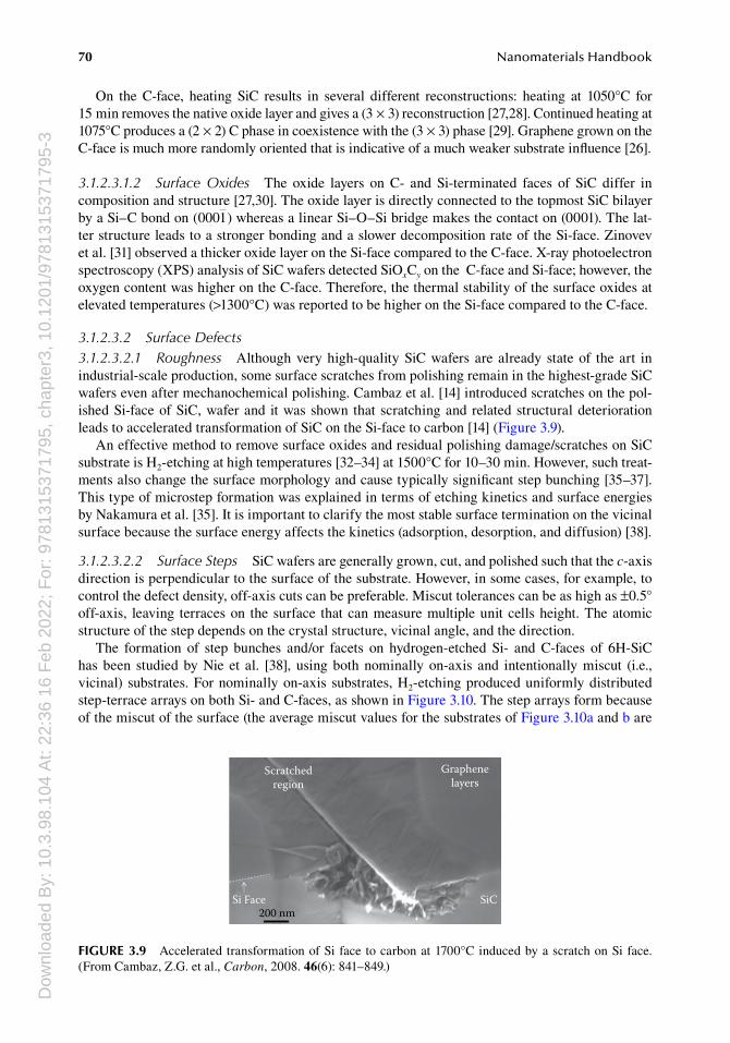
3.1.2.3.2 Surface Defects3.1.2.3.2.1 Roughness Although very high-quality SiC wafers are already state of the art in industrial-scale production, some surface scratches from polishing remain in the highest-grade SiC wafers even after mechanochemical polishing. Cambaz et al. [14] introduced scratches on the pol-ished Si-face of SiC, wafer and it was shown that scratching and related structural deterioration leads to accelerated transformation of SiC on the Si-face to carbon [14] (Figure 3.9).
An effective method to remove surface oxides and residual polishing damage/scratches on SiC substrate is H2-etching at high temperatures [32–34] at 1500°C for 10–30 min. However, such treat-ments also change the surface morphology and cause typically significant step bunching [35–37]. This type of microstep formation was explained in terms of etching kinetics and surface energies by Nakamura et al. [35]. It is important to clarify the most stable surface termination on the vicinal surface because the surface energy affects the kinetics (adsorption, desorption, and diffusion) [38].
3.1.2.3.2.2 Surface Steps SiC wafers are generally grown, cut, and polished such that the c-axis direction is perpendicular to the surface of the substrate. However, in some cases, for example, to control the defect density, off-axis cuts can be preferable. Miscut tolerances can be as high as ±0.5° off-axis, leaving terraces on the surface that can measure multiple unit cells height. The atomic structure of the step depends on the crystal structure, vicinal angle, and the direction.
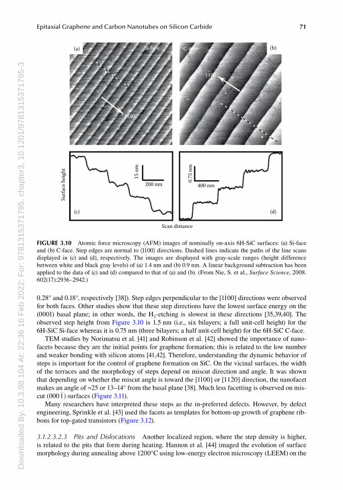
The formation of step bunches and/or facets on hydrogen-etched Si- and C-faces of 6H-SiC has been studied by Nie et al. [38], using both nominally on-axis and intentionally miscut (i.e., vicinal) substrates. For nominally on-axis substrates, H2-etching produced uniformly distributed step-terrace arrays on both Si- and C-faces, as shown in Figure 3.10. The step arrays form because of the miscut of the surface (the average miscut values for the substrates of Figure 3.10a and b are
Scratchedregion
Si Face200 nm
SiC
Graphenelayers
FIGURE 3.9 Accelerated transformation of Si face to carbon at 1700°C induced by a scratch on Si face. (From Cambaz, Z.G. et al., Carbon, 2008. 46(6): 841–849.)
Dow
nloa
ded
By:
10.
3.98
.104
At:
22:3
6 16
Feb
202
2; F
or: 9
7813
1537
1795
, cha
pter
3, 1
0.12
01/9
7813
1537
1795
-371Epitaxial Graphene and Carbon Nanotubes on Silicon Carbide
0.28° and 0.18°, respectively [38]). Step edges perpendicular to the [ ]1100 directions were observed for both faces. Other studies show that these step directions have the lowest surface energy on the (0001) basal plane; in other words, the H2-etching is slowest in these directions [35,39,40]. The observed step height from Figure 3.10 is 1.5 nm (i.e., six bilayers; a full unit-cell height) for the 6H-SiC Si-face whereas it is 0.75 nm (three bilayers; a half unit-cell height) for the 6H-SiC C-face.
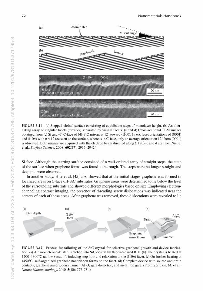
TEM studies by Norimatsu et al. [41] and Robinson et al. [42] showed the importance of nano-facets because they are the initial points for graphene formation; this is related to the low number and weaker bonding with silicon atoms [41,42]. Therefore, understanding the dynamic behavior of steps is important for the control of graphene formation on SiC. On the vicinal surfaces, the width of the terraces and the morphology of steps depend on miscut direction and angle. It was shown that depending on whether the miscut angle is toward the [1100] or [1120] direction, the nanofacet makes an angle of ≈25 or 13–14° from the basal plane [38]. Much less facetting is observed on mis-cut ( )0001 surfaces (Figure 3.11).
Many researchers have interpreted these steps as the in-preferred defects. However, by defect engineering, Sprinkle et al. [43] used the facets as templates for bottom-up growth of graphene rib-bons for top-gated transistors (Figure 3.12).
3.1.2.3.2.3 Pits and Dislocations Another localized region, where the step density is higher, is related to the pits that form during heating. Hannon et al. [44] imaged the evolution of surface morphology during annealing above 1200°C using low-energy electron microscopy (LEEM) on the
(a)
(c)
200 nm 400 nm
Surfa
ce h
eigh
t
15 n
m
0.75
nm
(d)
Scan distance
(b)Si-face
1100
C-face
–
1100–
FIGURE 3.10 Atomic force microscopy (AFM) images of nominally on-axis 6H-SiC surfaces: (a) Si-face and (b) C-face. Step edges are normal to ⟨1100⟩ directions. Dashed lines indicate the paths of the line scans displayed in (c) and (d), respectively. The images are displayed with gray-scale ranges (height difference between white and black gray levels) of (a) 1.4 nm and (b) 0.9 nm. A linear background subtraction has been applied to the data of (c) and (d) compared to that of (a) and (b). (From Nie, S. et al., Surface Science, 2008. 602(17):2936–2942.)
Dow
nloa
ded
By:
10.
3.98
.104
At:
22:3
6 16
Feb
202
2; F
or: 9
7813
1537
1795
, cha
pter
3, 1
0.12
01/9
7813
1537
1795
-372 Nanomaterials Handbook
Si-face. Although the starting surface consisted of a well-ordered array of straight steps, the state of the surface when graphene forms was found to be rough. The steps were no longer straight and deep pits were observed.
In another study, Hite et al. [45] also showed that at the initial stages graphene was formed in localized areas on C-face 6H-SiC substrates. Graphene areas were determined to lie below the level of the surrounding substrate and showed different morphologies based on size. Employing electron-channeling contrast imaging, the presence of threading screw dislocations was indicated near the centers of each of these areas. After graphene was removed, these dislocations were revealed to lie
(a)
(b)
(c)
(d)
Si face
C face
Miscut at 12° toward <1–100>
Miscut at 12° toward <1–100>
(1–10n)
Atomic step
Miscut angle
Step bunch Terrace
(0001)
20 nm
20 nm
FIGURE 3.11 (a) Stepped vicinal surface consisting of equidistant steps of monolayer height. (b) An alter-nating array of singular facets (terraces) separated by vicinal facets. (c and d) Cross-sectional TEM images obtained from (c) Si and (d) C-face of 6H-SiC miscut at 12° toward ⟨1100⟩. In (c), facet orientations of (0001) and ( )110n with n ≈ 12 are seen on the surface, whereas in C-face, only an average orientation 12° from ( )0001 is observed. Both images are acquired with the electron beam directed along ⟨1120⟩ (c and d are from Nie, S. et al., Surface Science, 2008. 602(17): 2936–2942.)
Etch depth(a) (b) (c) (d)
SiCSiC
(110n)facet Drain
Graphenenanoribbon Source
GateAl2O3
FIGURE 3.12 Process for tailoring of the SiC crystal for selective graphene growth and device fabrica-tion. (a) A nanometer-scale step is etched into SiC crystal by fluorine-based RIE. (b) The crystal is heated at 1200–1300°C (at low vacuum), inducing step flow and relaxation to the ( )110n facet. (c) On further heating at 1450°C, self-organized graphene nanoribbon forms on the facet. (d) Complete device with source and drain contacts, graphene nanoribbon channel, Al2O3 gate dielectric, and metal top gate. (From Sprinkle, M. et al., Nature Nanotechnology, 2010. 5(10): 727–731.)
Dow
nloa
ded
By:
10.
3.98
.104
At:
22:3
6 16
Feb
202
2; F
or: 9
7813
1537
1795
, cha
pter
3, 1
0.12
01/9
7813
1537
1795
-373Epitaxial Graphene and Carbon Nanotubes on Silicon Carbide
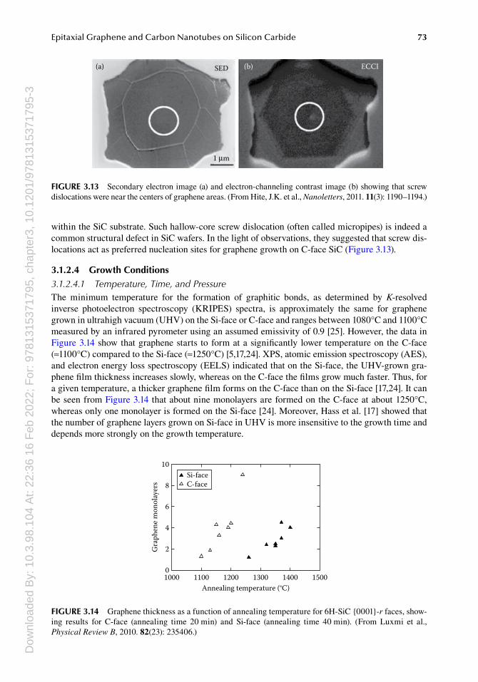
within the SiC substrate. Such hallow-core screw dislocation (often called micropipes) is indeed a common structural defect in SiC wafers. In the light of observations, they suggested that screw dis-locations act as preferred nucleation sites for graphene growth on C-face SiC (Figure 3.13).
3.1.2.4 Growth Conditions3.1.2.4.1 Temperature, Time, and PressureThe minimum temperature for the formation of graphitic bonds, as determined by K-resolved inverse photoelectron spectroscopy (KRIPES) spectra, is approximately the same for graphene grown in ultrahigh vacuum (UHV) on the Si-face or C-face and ranges between 1080°C and 1100°C measured by an infrared pyrometer using an assumed emissivity of 0.9 [25]. However, the data in Figure 3.14 show that graphene starts to form at a significantly lower temperature on the C-face (≈1100°C) compared to the Si-face (≈1250°C) [5,17,24]. XPS, atomic emission spectroscopy (AES), and electron energy loss spectroscopy (EELS) indicated that on the Si-face, the UHV-grown gra-phene film thickness increases slowly, whereas on the C-face the films grow much faster. Thus, for a given temperature, a thicker graphene film forms on the C-face than on the Si-face [17,24]. It can be seen from Figure 3.14 that about nine monolayers are formed on the C-face at about 1250°C, whereas only one monolayer is formed on the Si-face [24]. Moreover, Hass et al. [17] showed that the number of graphene layers grown on Si-face in UHV is more insensitive to the growth time and depends more strongly on the growth temperature.
SED(a) (b)
1 μm
ECCI
FIGURE 3.13 Secondary electron image (a) and electron-channeling contrast image (b) showing that screw dislocations were near the centers of graphene areas. (From Hite, J.K. et al., Nanoletters, 2011. 11(3): 1190–1194.)
10Si-faceC-face8
6
Gra
phen
e mon
olay
ers
4
2
01000 1100 1200 1300
Annealing temperature (°C)1400 1500
FIGURE 3.14 Graphene thickness as a function of annealing temperature for 6H-SiC {0001}-r faces, show-ing results for C-face (annealing time 20 min) and Si-face (annealing time 40 min). (From Luxmi et al., Physical Review B, 2010. 82(23): 235406.)
Dow
nloa
ded
By:
10.
3.98
.104
At:
22:3
6 16
Feb
202
2; F
or: 9
7813
1537
1795
, cha
pter
3, 1
0.12
01/9
7813
1537
1795
-374 Nanomaterials Handbook
Kusunoki et al. [2] also studied the effect of temperature, time, and pressure. SiC wafers were heated at several temperatures (1300°C, 1500°C, and 1700°C) for 0.5 h in a vacuum of 1 × 10⁻⁴ Torr, then were observed using TEM. At 1500°C, the length of the CNTs formed was 50 and 180 nm for 0.5 and 6 h, respectively. Moreover, when a wafer was heated at 1500°C for 0.5 h in a better vacuum (1 × 10⁻⁶ Torr), the length of the CNTs was only 25 nm; thus, decreasing the pressure results in CNTs with a shorter length.
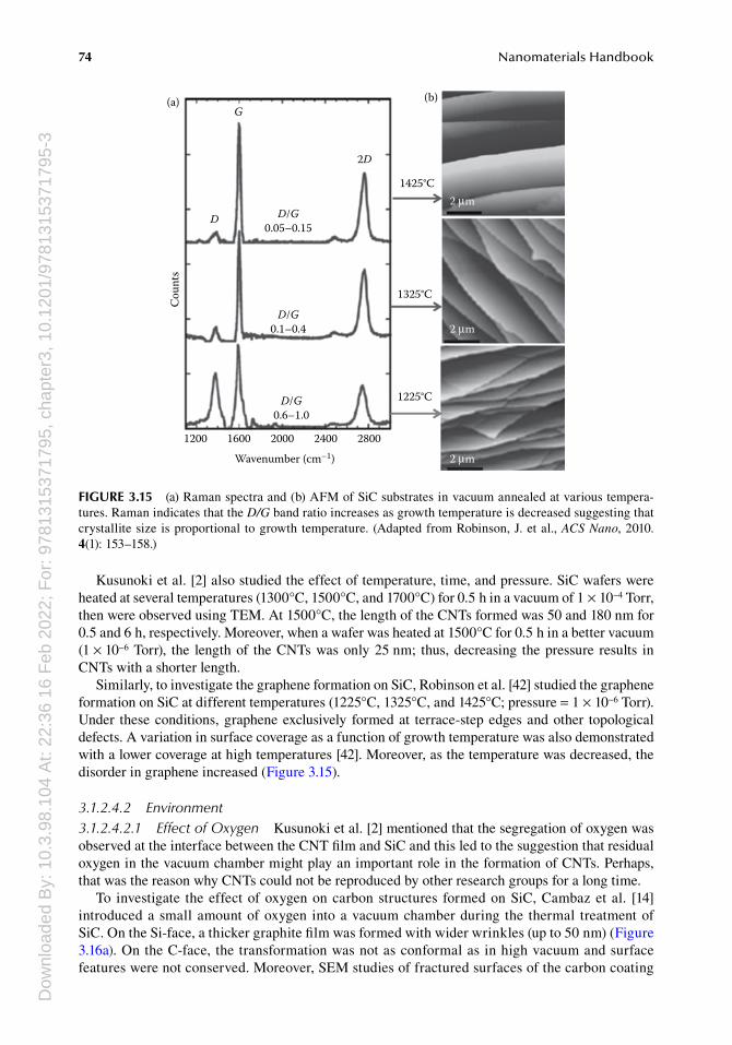
Similarly, to investigate the graphene formation on SiC, Robinson et al. [42] studied the graphene formation on SiC at different temperatures (1225°C, 1325°C, and 1425°C; pressure = 1 × 10⁻⁶ Torr). Under these conditions, graphene exclusively formed at terrace-step edges and other topological defects. A variation in surface coverage as a function of growth temperature was also demonstrated with a lower coverage at high temperatures [42]. Moreover, as the temperature was decreased, the disorder in graphene increased (Figure 3.15).
3.1.2.4.2 Environment3.1.2.4.2.1 Effect of Oxygen Kusunoki et al. [2] mentioned that the segregation of oxygen was observed at the interface between the CNT film and SiC and this led to the suggestion that residual oxygen in the vacuum chamber might play an important role in the formation of CNTs. Perhaps, that was the reason why CNTs could not be reproduced by other research groups for a long time.
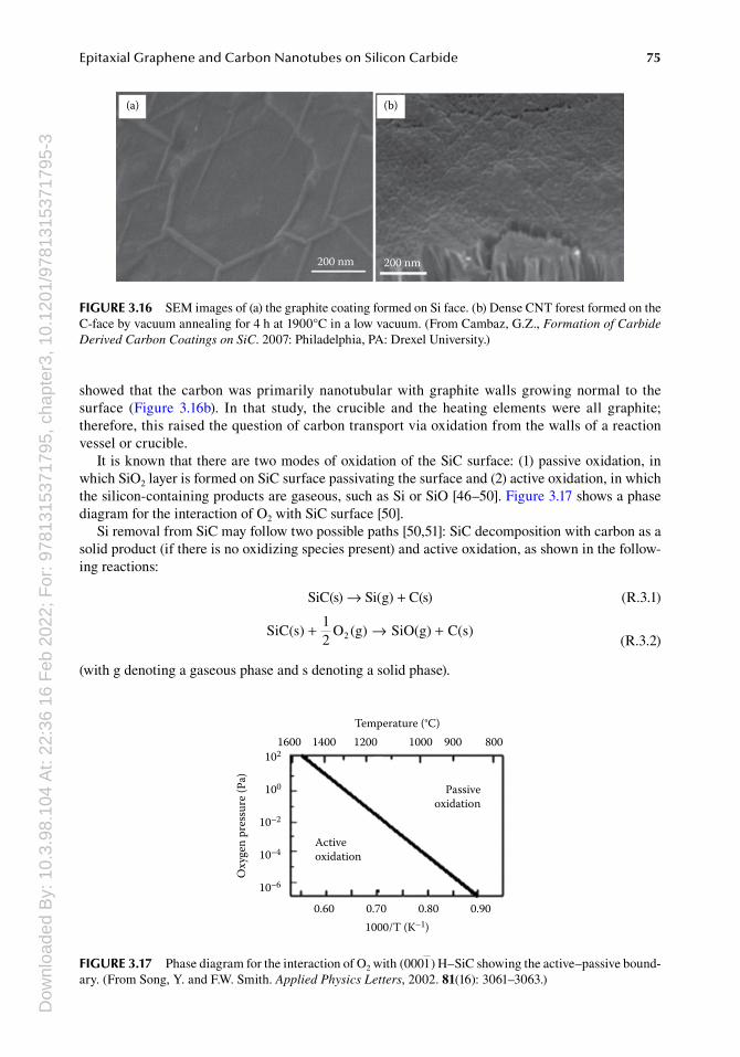
To investigate the effect of oxygen on carbon structures formed on SiC, Cambaz et al. [14] introduced a small amount of oxygen into a vacuum chamber during the thermal treatment of SiC. On the Si-face, a thicker graphite film was formed with wider wrinkles (up to 50 nm) (Figure 3.16a). On the C-face, the transformation was not as conformal as in high vacuum and surface features were not conserved. Moreover, SEM studies of fractured surfaces of the carbon coating
Coun
ts
G
D
2D
D/G0.05–0.15
(a) (b)
D/G
D/G
0.1–0.4
0.6–1.0
1200 1600Wavenumber (cm–1)
2000 2400 2800
1425°C
1325°C
1225°C
2 μm
2 μm
2 μm
FIGURE 3.15 (a) Raman spectra and (b) AFM of SiC substrates in vacuum annealed at various tempera-tures. Raman indicates that the D/G band ratio increases as growth temperature is decreased suggesting that crystallite size is proportional to growth temperature. (Adapted from Robinson, J. et al., ACS Nano, 2010. 4(1): 153–158.)
Dow
nloa
ded
By:
10.
3.98
.104
At:
22:3
6 16
Feb
202
2; F
or: 9
7813
1537
1795
, cha
pter
3, 1
0.12
01/9
7813
1537
1795
-375Epitaxial Graphene and Carbon Nanotubes on Silicon Carbide
showed that the carbon was primarily nanotubular with graphite walls growing normal to the surface (Figure 3.16b). In that study, the crucible and the heating elements were all graphite; therefore, this raised the question of carbon transport via oxidation from the walls of a reaction vessel or crucible.
It is known that there are two modes of oxidation of the SiC surface: (1) passive oxidation, in which SiO2 layer is formed on SiC surface passivating the surface and (2) active oxidation, in which the silicon-containing products are gaseous, such as Si or SiO [46–50]. Figure 3.17 shows a phase diagram for the interaction of O2 with SiC surface [50].
Si removal from SiC may follow two possible paths [50,51]: SiC decomposition with carbon as a solid product (if there is no oxidizing species present) and active oxidation, as shown in the follow-ing reactions:
SiC(s) → Si(g) + C(s) (R.3.1)
SiC(s) O (g) SiO(g) C(s)2+ → +1
2 (R.3.2)
(with g denoting a gaseous phase and s denoting a solid phase).
(a) (b)
200 nm 200 nm
FIGURE 3.16 SEM images of (a) the graphite coating formed on Si face. (b) Dense CNT forest formed on the C-face by vacuum annealing for 4 h at 1900°C in a low vacuum. (From Cambaz, G.Z., Formation of Carbide Derived Carbon Coatings on SiC. 2007: Philadelphia, PA: Drexel University.)
Temperature (°C)
Passiveoxidation
Activeoxidation
1600102
100
10–2
10–4
10–6
Oxy
gen
pres
sure
(Pa)
1400
0.60 0.701000/T (K–1)
0.80 0.90
1200 1000 900 800
FIGURE 3.17 Phase diagram for the interaction of O2 with ( )0001 H–SiC showing the active–passive bound-ary. (From Song, Y. and F.W. Smith. Applied Physics Letters, 2002. 81(16): 3061–3063.)
Dow
nloa
ded
By:
10.
3.98
.104
At:
22:3
6 16
Feb
202
2; F
or: 9
7813
1537
1795
, cha
pter
3, 1
0.12
01/9
7813
1537
1795
-376 Nanomaterials Handbook
The rate of SiC Reaction 3.1 is faster than that of Reaction 3.2 [50]. Additionally, taking into account that all lining and heating elements inside the vacuum furnace are made of carbon; carbon transport may occur in the presence of oxygen by Reaction 3.3 (Bouduard reaction).
2C(s) + O2(g) ↔ 2CO(g) (R.3.3)
These results suggest that at higher oxygen pressures, the carbon-formation rate is increased due to the parallel processes of Reactions 3.1 through 3.3 including gas-phase carbon transport.
3.1.2.4.2.2 Effect of Crucible To investigate the hypothesis that carbon transport occurs from carbon lining, Cambaz [16] placed SiC wafers with the Si face and C face down onto graphite plates, assuming that a short distance (compared to the transport from the crucible or remote furnace heat-ers) would assist and accelerate the transport.
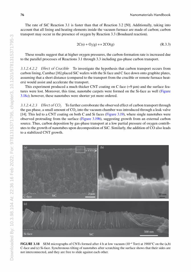
This experiment produced a much thicker CNT coating on C face (≈9 µm) and the surface fea-tures were lost. Moreover, this time, nanotube carpets were formed on the Si-face as well (Figure 3.18c); however, these nanotubes were shorter yet more ordered.
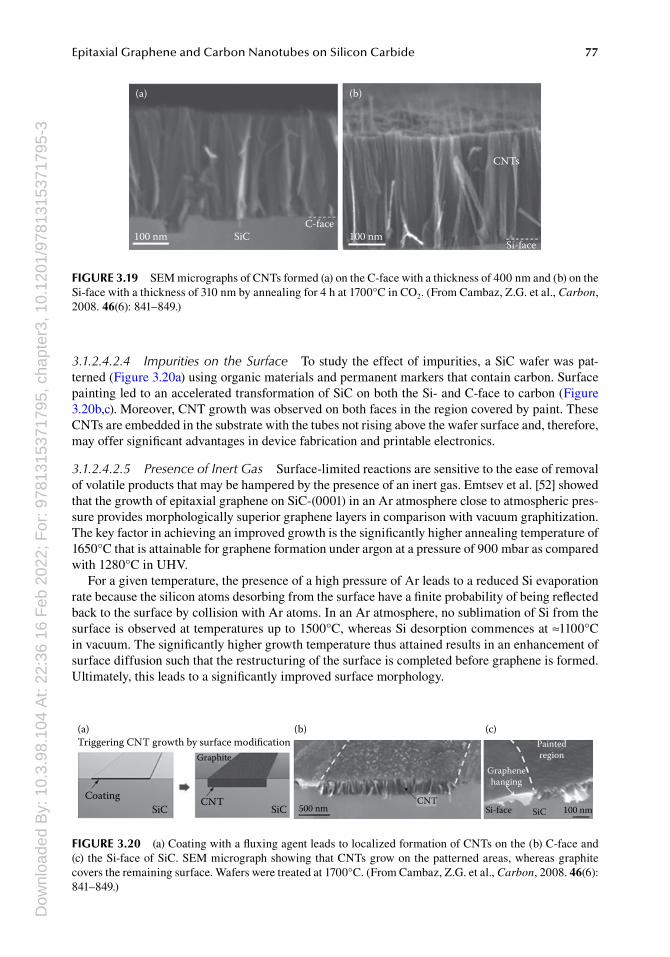
3.1.2.4.2.3 Effect of CO2 To further corroborate the observed effect of carbon transport through the gas phase, a small amount of CO2 into the vacuum chamber was introduced through a leak valve [14]. This led to a CNT coating on both C and Si faces (Figure 3.19), where single nanotubes were observed protruding from the surface (Figure 3.19b), suggesting growth from an external carbon source. Thus, carbon deposition by gas-phase transport at a low partial pressure of oxygen contrib-utes to the growth of nanotubes upon decomposition of SiC. Similarly, the addition of CO also leads to a stabilized CNT growth.
(a)
(c)
(b)
C-face
Si-face
SiC
SiC500 nm
50 nm2 μm
FIGURE 3.18 SEM micrographs of CNTs formed after 4 h at low vacuum (10−4 Torr) at 1900°C on the (a,b) C-face and (c) Si-face. Synchronous tilting of nanotubes after scratching the surface shows that their sides are not interconnected, and they are free to slide against each other.
Dow
nloa
ded
By:
10.
3.98
.104
At:
22:3
6 16
Feb
202
2; F
or: 9
7813
1537
1795
, cha
pter
3, 1
0.12
01/9
7813
1537
1795
-377Epitaxial Graphene and Carbon Nanotubes on Silicon Carbide
3.1.2.4.2.4 Impurities on the Surface To study the effect of impurities, a SiC wafer was pat-terned (Figure 3.20a) using organic materials and permanent markers that contain carbon. Surface painting led to an accelerated transformation of SiC on both the Si- and C-face to carbon (Figure 3.20b,c). Moreover, CNT growth was observed on both faces in the region covered by paint. These CNTs are embedded in the substrate with the tubes not rising above the wafer surface and, therefore, may offer significant advantages in device fabrication and printable electronics.
3.1.2.4.2.5 Presence of Inert Gas Surface-limited reactions are sensitive to the ease of removal of volatile products that may be hampered by the presence of an inert gas. Emtsev et al. [52] showed that the growth of epitaxial graphene on SiC-(0001) in an Ar atmosphere close to atmospheric pres-sure provides morphologically superior graphene layers in comparison with vacuum graphitization. The key factor in achieving an improved growth is the significantly higher annealing temperature of 1650°C that is attainable for graphene formation under argon at a pressure of 900 mbar as compared with 1280°C in UHV.
For a given temperature, the presence of a high pressure of Ar leads to a reduced Si evaporation rate because the silicon atoms desorbing from the surface have a finite probability of being reflected back to the surface by collision with Ar atoms. In an Ar atmosphere, no sublimation of Si from the surface is observed at temperatures up to 1500°C, whereas Si desorption commences at ≈1100°C in vacuum. The significantly higher growth temperature thus attained results in an enhancement of surface diffusion such that the restructuring of the surface is completed before graphene is formed. Ultimately, this leads to a significantly improved surface morphology.
(a) (b)
100 nm 100 nm
CNTs
SiCC-face
Si-face
FIGURE 3.19 SEM micrographs of CNTs formed (a) on the C-face with a thickness of 400 nm and (b) on the Si-face with a thickness of 310 nm by annealing for 4 h at 1700°C in CO2. (From Cambaz, Z.G. et al., Carbon, 2008. 46(6): 841–849.)
Triggering CNT growth by surface modification(a) (b) (c)
CoatingSiC SiC
CNT
Graphite
500 nmCNT
Graphenehanging
Paintedregion
Si-face SiC 100 nm
FIGURE 3.20 (a) Coating with a fluxing agent leads to localized formation of CNTs on the (b) C-face and (c) the Si-face of SiC. SEM micrograph showing that CNTs grow on the patterned areas, whereas graphite covers the remaining surface. Wafers were treated at 1700°C. (From Cambaz, Z.G. et al., Carbon, 2008. 46(6): 841–849.)
Dow
nloa
ded
By:
10.
3.98
.104
At:
22:3
6 16
Feb
202
2; F
or: 9
7813
1537
1795
, cha
pter
3, 1
0.12
01/9
7813
1537
1795
-378 Nanomaterials Handbook
3.1.3 cnt anD grapHene-formation mecHanism on sic
Explanation of all the details is not easily verified because in situ investigation of the aforemen-tioned processes is hard and limited at high temperatures. However, imaging the produced features on the surface with atomic-scale resolution (using AFM, SPM, and HRTEM) provided consider-able insight into the growth mechanism of carbon on SiC. Studies showed that the resultant carbon structure strongly depends on the nucleation rate of carbon at the initial stages. If the nucleation rate is high, nonuniform nucleation takes place as islands on the terraces on the (0001)-surface. This mostly results in disordered thick graphitic structures. However, if there is an extra carbon supply present, whether by CO, CO2, or carbon transport from the crucible walls through oxidation, these islands become curved forming distinct caps that turn into CNTs as the reaction proceeds.
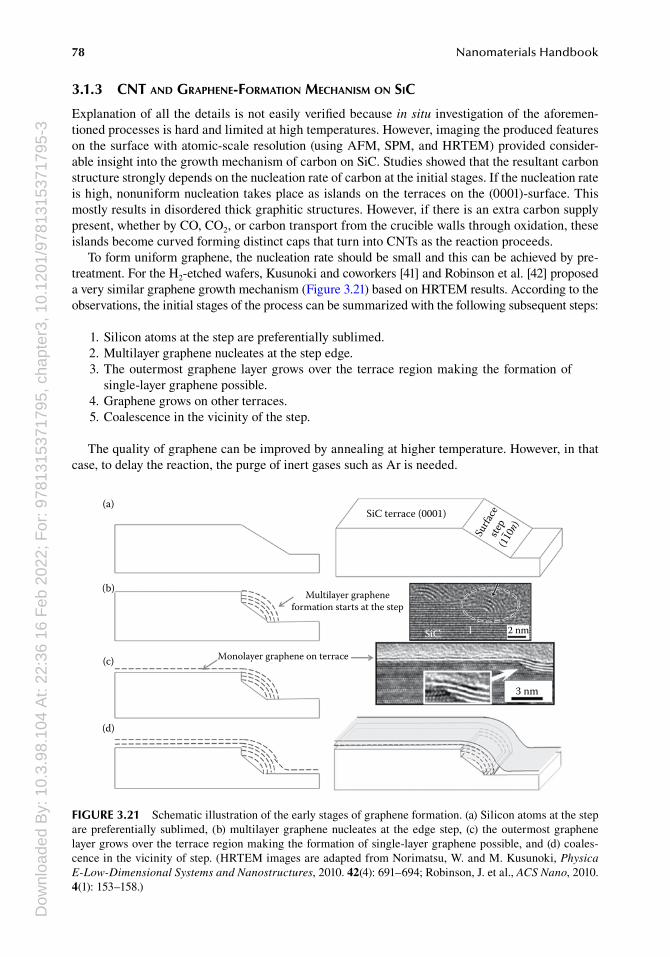
To form uniform graphene, the nucleation rate should be small and this can be achieved by pre-treatment. For the H2-etched wafers, Kusunoki and coworkers [41] and Robinson et al. [42] proposed a very similar graphene growth mechanism (Figure 3.21) based on HRTEM results. According to the observations, the initial stages of the process can be summarized with the following subsequent steps:
1. Silicon atoms at the step are preferentially sublimed. 2. Multilayer graphene nucleates at the step edge. 3. The outermost graphene layer grows over the terrace region making the formation of
single-layer graphene possible. 4. Graphene grows on other terraces. 5. Coalescence in the vicinity of the step.
The quality of graphene can be improved by annealing at higher temperature. However, in that case, to delay the reaction, the purge of inert gases such as Ar is needed.
SiC terrace (0001)(a)
(b)
(c)
(d)
Multilayer grapheneformation starts at the step
SiC I 2 nm
3 nm
Monolayer graphene on terrace
Surfa
ce
step
(110
n)
FIGURE 3.21 Schematic illustration of the early stages of graphene formation. (a) Silicon atoms at the step are preferentially sublimed, (b) multilayer graphene nucleates at the edge step, (c) the outermost graphene layer grows over the terrace region making the formation of single-layer graphene possible, and (d) coales-cence in the vicinity of step. (HRTEM images are adapted from Norimatsu, W. and M. Kusunoki, Physica E-Low-Dimensional Systems and Nanostructures, 2010. 42(4): 691–694; Robinson, J. et al., ACS Nano, 2010. 4(1): 153–158.)
Dow
nloa
ded
By:
10.
3.98
.104
At:
22:3
6 16
Feb
202
2; F
or: 9
7813
1537
1795
, cha
pter
3, 1
0.12
01/9
7813
1537
1795
-379Epitaxial Graphene and Carbon Nanotubes on Silicon Carbide
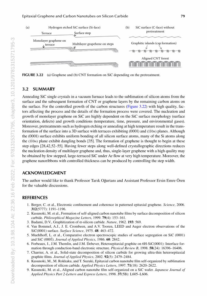
3.2 SUMMARY
Annealing SiC single crystals in a vacuum furnace leads to the sublimation of silicon atoms from the surface and the subsequent formation of CNT or graphene layers by the remaining carbon atoms on the surface. For the controlled growth of the carbon structures (Figure 3.22) with high quality, fac-tors affecting the process and the details of the formation process were covered. The nucleation and growth of monolayer graphene on SiC are highly dependent on the SiC surface morphology (surface orientation, defects) and growth conditions (temperature, time, pressure, and environmental gases). Moreover, pretreatments such as hydrogen etching or annealing at high temperature result in the trans-formation of the surface into a 3D surface with terraces exhibiting (0001) and ( )110n planes. Although the (0001) surface exhibits uniform bonding of all silicon surface atoms, many of the Si atoms along the ( )110n plane exhibit dangling bonds [35]. The formation of graphene is thought to begin at these step edges [28,42,52–55]. Having fewer steps along well-defined crystallographic directions reduces the nucleation density of multilayer graphene and, thus, single-layer graphene with a high quality may be obtained by few stepped, large-terraced SiC under Ar flow at very high temperature. Moreover, the graphene nanoribbons with controlled thickness can be produced by controlling the step width.
ACKNOWLEDGMENT
The author would like to thank Professor Tarık Ogurtanı and Assistant Professor Ersin Emre Ören for the valuable discussions.
REFERENCES
1. Berger, C. et al., Electronic confinement and coherence in patterned epitaxial graphene. Science, 2006. 312(5777): 1191–1196.
2. Kusunoki, M. et al., Formation of self-aligned carbon nanotube films by surface decomposition of silicon carbide. Philosophical Magazine Letters, 1999. 79(4): 153–161.
3. Badami, D.V., Graphitization of α-silicon carbide. Nature, 1962. 193: 569. 4. Van Bommel, A.J., J. E. Crombeen, and A.V. Tooren, LEED and Auger electron observations of the
SiC(0001) surface. Surface Science, 1975. 48: 463–472. 5. Muehlhoff, L. et al., Comparative electron spectroscopic studies of surface segregation on SiC (0001)
and SiC (0001). Journal of Applied Physics, 1986. 60: 2842. 6. Forbeaux, I., J.M. Themlin, and J.M. Debever, Heteroepitaxial graphite on 6H-SiC(0001): Interface for-
mation through conduction-band electronic structure. Physical Review B, 1998. 58(24): 16396–16406. 7. Charrier, A. et al., Solid-state decomposition of silicon carbide for growing ultra-thin heteroepitaxial
graphite films. Journal of Applied Physics, 2002. 92(5): 2479–2484. 8. Kusunoki, M., M. Rokkaku, and T. Suzuki, Epitaxial carbon nanotube film self-organized by sublimation
decomposition of silicon carbide. Applied Physics Letters, 1997. 71(18): 2620–2622. 9. Kusunoki, M. et al., Aligned carbon nanotube film self-organized on a SiC wafer. Japanese Journal of
Applied Physics Part 2-Letters and Express Letters, 1998. 37(5B): L605–L606.
Hydrogen etched SiC surface (Si-face) SiC surface (C-face) without pretreatment
Graphitic islands (cap formation)
Aligned CNT forest
Terrace
(a) (b)Surface step
Monolayer graphene on terrace Multilayer grapehene on steps
FIGURE 3.22 (a) Graphene and (b) CNT formation on SiC depending on the pretreatment.
Dow
nloa
ded
By:
10.
3.98
.104
At:
22:3
6 16
Feb
202
2; F
or: 9
7813
1537
1795
, cha
pter
3, 1
0.12
01/9
7813
1537
1795
-380 Nanomaterials Handbook
10. Kusunoki, M. et al., A formation mechanism of carbon nanotube films on SiC(0001). Applied Physics Letters, 2000. 77(4): 531–533.
11. Watanabe, H. et al., In situ observation of the initial growth process of carbon nanotubes by time resolved high resolution transmission electron microscopy. Journal of Microscopy, 2001. 203(1): 40–46.
12. Novoselov, K.S. et al., Electric field effect in atomically thin carbon films. Science, 2004. 306(5696): 666–669.
13. Berger, C. et al., Ultrathin epitaxial graphite: 2D electron gas properties and a route toward graphene-based nanoelectronics. Journal of Physical Chemistry B, 2004. 108(52): 19912–19916.
14. Cambaz, Z.G. et al., Noncatalytic synthesis of carbon nanotubes, graphene and graphite on SiC. Carbon, 2008. 46(6): 841–849.
15. Saddow, S.E. and A. Agarwal, Advances in Silicon Carbide Processing and Applications. 2004: Norwood: Artech House Publishers.
16. Cambaz, G.Z., Formation of Carbide Derived Carbon Coatings on SiC, in Materials Science and Engineering. 2007: Philadelphia, PA: Drexel University.
17. Hass, J., W.A. de Heer, and E.H. Conrad, The growth and morphology of epitaxial multilayer graphene. Journal of Physics-Condensed Matter, 2008. 20(32): 323202.
18. Cambaz, Z.G. et al., Formation of carbide-derived carbon on beta-silicon carbide whiskers. Journal of the American Ceramic Society, 2006. 89(2): 509–514.
19. Kusunoki, M. et al., Selective synthesis of zigzag-type aligned carbon nanotubes on SiC (000-1) wafers. Chemical Physics Letters, 2002. 366(5–6): 458–462.
20. Kusunoki, M., High-density and well-aligned carbon nanotube films on silicon-carbide wafers. Journal of the Ceramic Society of Japan, 2005. 113(1322): 637–641.
21. Powell, J.A., P. Pirouz, and W.J. Choyke, Growth and characterization of silicon carbide polytypes for electronic applications, in Semiconductor Interfaces, Microstructures, and Devices: Properties and Applications, Z.C. Feng, ed. 1993: UK: Institute of Physics Publishing: p. 257.
22. Srivastava, N. et al., Graphene formed on SiC under various environments: Comparison of Si-face and C-face. Journal of Physics D-Applied Physics, 2012. 45(15): 154001.
23. Luxmi et al., Morphology of graphene on SiC(0001) surfaces. Applied Physics Letters, 2009. 95(7): 3207757.
24. Luxmi et al., Comparison of graphene formation on C-face and Si-face SiC {0001} surfaces. Physical Review B, 2010. 82(23): 235406.
25. Forbeaux, I. et al., Solid-state graphitization mechanisms of silicon carbide 6H-SiC polar faces. Applied Surface Science, 2000. 162: 406–412.
26. Hass, J. et al., Highly ordered graphene for two dimensional electronics. Applied Physics Letters, 2006. 89(14): 143106.
27. Bernhardt, J. et al., Epitaxially ideal oxide–semiconductor interfaces: Silicate adlayers on hexagonal (0001) and (000(1)over-bar) SiC surfaces. Applied Physics Letters, 1999. 74(8): 1084–1086.
28. Johansson, L.I., P.A. Glans, and N. Hellgren, A core level and valence band photoemission study of 6H-SiC(000(1)over-bar). Surface Science, 1998. 405(2–3): 288–297.
29. Bernhardt, J. et al., Stable surface reconstructions on 6H-SiC(0001). Materials Science and Engineering B-Solid State Materials for Advanced Technology, 1999. 61–2: 207–211.
30. Nagano, T., Y. Ishikawa, and N. Shibata, Effects of surface oxides of SiC on carbon nanotube formation by surface decomposition. Japanese Journal of Applied Physics Part 1-Regular Papers Short Notes and Review Papers, 2003. 42(3): 1380–1385.
31. Zinovev, A.V. et al., Etching of hexagonal SiC surfaces in chlorine-containing gas media at ambient pres-sure. Surface Science, 2006. 600(11): 2242–2251.
32. Berger, C. et al., Electronic confinement and coherence in patterned epitaxial graphene. Science, 2006. 312(5777): 1191–1196.
33. de Heer, W.A. et al., Epitaxial graphene. Solid State Communications, 2007. 143(1–2): 92–100. 34. Emtsev, K.V. et al., Towards wafer-size graphene layers by atmospheric pressure graphitization of silicon
carbide. Nature Materials, 2009. 8(3): 203–207. 35. Nakamura, S. et al., Formation of periodic steps with a unit-cell height on 6H-SiC (0001) surface by HCl
etching. Applied Physics Letters, 2000. 76(23): 3412–3414. 36. Fujii, M. and S. Tanaka, Ordering distance of surface nanofacets on vicinal 4H-SiC(0001). Physical
Review Letters, 2007. 99(1): 016102. 37. Hayashi, K. et al., Stable surface termination on vicinal 6H-SiC(0001) surfaces. Surface Science, 2009.
603(3): 566–570.
Dow
nloa
ded
By:
10.
3.98
.104
At:
22:3
6 16
Feb
202
2; F
or: 9
7813
1537
1795
, cha
pter
3, 1
0.12
01/9
7813
1537
1795
-381Epitaxial Graphene and Carbon Nanotubes on Silicon Carbide
38. Nie, S. et al., Step formation on hydrogen-etched 6H-SiC{0001} surfaces. Surface Science, 2008. 602(17): 2936–2942.
39. Wulfhekel, W. et al., Regular step formation on concave-shaped surfaces on 6H-SiC(0001). Surface Science, 2004. 550(1–3): 8–14.
40. Nakajima, A. et al., Step control of vicinal 6H-SiC(0001) surface by H2 etching. Journal of Applied Physics, 2005. 97(10): 104919.
41. Norimatsu, W. and M. Kusunoki, Formation process of graphene on SiC (0001). Physica E-Low-Dimensional Systems and Nanostructures, 2010. 42(4): 691–694.
42. Robinson, J. et al., Nucleation of epitaxial graphene on SiC(0001). ACS Nano, 2010. 4(1): 153–158. 43. Sprinkle, M. et al., Scalable templated growth of graphene nanoribbons on SiC. Nature Nanotechnology,
2010. 5(10): 727–731. 44. Hannon, J.B. and R.M. Tromp, Pit formation during graphene synthesis on SiC(0001): In situ electron
1190–1194. 46. Luthra, K.L., Some new perspectives on oxidation of silicon carbide and silicon nitride. Journal of the
American Ceramic Society, 1991. 74(5): 1095–1103. 47. Balat, M. et al., Active to passive transition in the oxidation of silicon carbide at high temperature and low
pressure in molecular and atomic oxygen. Journal of Materials Science, 1992. 27(3): 697–703. 48. Schneider, B. et al., A theoretical and experimental approach to the active-to-passive transition in the
oxidation of silicon carbide—Experiments at high temperatures and low total pressures. Journal of Materials Science, 1998. 33(2): 535–547.
49. Goto, T. and H. Homma, High-temperature active/passive oxidation and bubble formation of CVD SiC in O2 and CO2 atmospheres. Journal of the European Ceramic Society, 2002. 22(14–15): 2749–2756.
50. Song, Y. and F.W. Smith, Phase diagram for the interaction of oxygen with SiC. Applied Physics Letters, 2002. 81(16): 3061–3063.
51. Maruyama, T. et al., STM and XPS studies of early stages of carbon nanotube growth by surface decom-position of 6H-SiC(000-1) under various oxygen pressures. Diamond and Related Materials, 2007. 16(4–7): 1078–1081.
52. Emtsev, K.V. et al., Towards wafer-size graphene layers by atmospheric pressure graphitization of silicon carbide. Nature Materials, 2009. 8(3): 203–207.
53. Hupalo, M., E.H. Conrad, and M.C. Tringides, Growth mechanism for epitaxial graphene on vicinal 6H-SiC(0001) surfaces: A scanning tunneling microscopy study. Physical Review B, 2009. 80(4): 041401.
54. Poon, S.W. et al., Probing epitaxial growth of graphene on silicon carbide by metal decoration. Applied Physics Letters, 2008. 92(10): 104102.
55. Virojanadara, C. et al., Substrate orientation: A way towards higher quality monolayer graphene growth on 6H-SiC(0001). Surface Science, 2009. 603(15): L87–L90.