Hamburg 2019: NanoPhononics Workshop Zlatan Aksamija NanoEnergy&Thermophysics lab University of Massachusetts at Amherst [email protected]http://netlab.umasscreate.net PIER, Hamburg 2019 Nanophononics Workshop Nanophononics: dissipation and thermoelectric energy conversion in nanoscale devices
Nanophononics: dissipation and thermoelectric energy conversion in
nanoscale devices
2Zlatan Aksamija, NETlab@UMass-Amherst
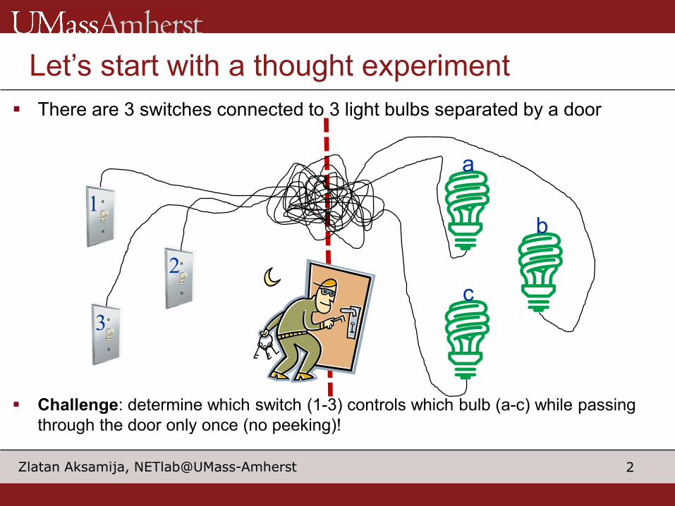
Let’s start with a thought experiment There are 3 switches connected to 3 light bulbs separated by a door
Challenge: determine which switch (1-3) controls which bulb (a-c) while passing through the door only once (no peeking)!
1
2
3
a
b
c
3Zlatan Aksamija, NETlab@UMass-Amherst
Answer: use the “thermal signature”! Flip switch #1, wait 5 mins. Then flip switch #2 and go through Solution: hot bulb is connected to #1, the lit bulb is connected to #2
Moral: Heat stores and transmits useful information, a “thermal signature”, of a process and is the ultimate destination of all the energy we use!
1
2
3
a
b
c
4Zlatan Aksamija, NETlab@UMass-Amherst
At the dawn of time…
First there were vacuum tubes Invented in 1904 by John Ambrose Fleming Diodes, triodes, pentodes, miniatures Still used for extreme environments
• ex. Viktor Belenko deflected from the USSR to Japan/US with his MIG-25 fighter jet in 1976, all electronics were using vacuum tubes
Or extreme audiophiles (ex. guitar amps, studio gear) Simple operation: heat up a metals and electrons will “boil”
off the cathode, add a grid to control them Issues: heat/energy, reliability
5Zlatan Aksamija, NETlab@UMass-Amherst
Enter the transistor Invented by 1947 by John Bardeen, Walter Brattain,
and William Shockley at Bell Labs First transistor was a “point contact” transistor Shared the Nobel Prize in Physics in 1956 One of IEEE milestones in electronics Requires no heating Can be bipolar (!?!) Small, reliable, efficient
6Zlatan Aksamija, NETlab@UMass-Amherst
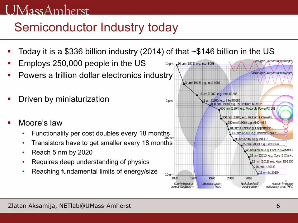
Semiconductor Industry today
Today it is a $336 billion industry (2014) of that ~$146 billion in the US Employs 250,000 people in the US Powers a trillion dollar electronics industry
Driven by miniaturization
Moore’s law• Functionality per cost doubles every 18 months• Transistors have to get smaller every 18 months• Reach 5 nm by 2020• Requires deep understanding of physics• Reaching fundamental limits of energy/size
7Zlatan Aksamija, NETlab@UMass-Amherst
Semiconductor Industry Tomorrow End of “simple scaling”—no longer can follow Moore’s Law by making
transistors smaller• Short channel effects—can’t turn transistors off any more due to quantum mechanics• Power catastrophe—dissipation limits performance, density, clock frequency
New materials• Seamless integration of compound semiconductors (ex. GaAs channel)• 2-dimensional materials: graphene, MoS2, other TMDCs
New functionality• Optoelectronic integration, on-chip optical interconnects• Energy devices like thermoelectric converters and on-chip cooling• 2-terminal devices such as memristors and neuromorphic (brain-like) computing
8Zlatan Aksamija, NETlab@UMass-Amherst
9Zlatan Aksamija, NETlab@UMass-Amherst
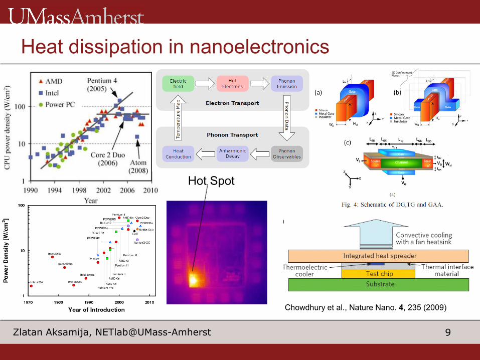
Heat dissipation in nanoelectronics
Chowdhury et al., Nature Nano. 4, 235 (2009)
Hot Spot
10Zlatan Aksamija, NETlab@UMass-Amherst
Electro-thermal simulation of devices Basic idea is to solve MC electron transport together with MC for phonons
being emitted/absorbed by the electrons
Also need to solve for heat conduction away from MC region
11Zlatan Aksamija, NETlab@UMass-Amherst
Electro-thermal simulation of devices Self-heating in nanoscale MOSFET devices results in current degradation We can see the inclusion of thermal effects results in the code converging to
lower drain current (left) Current degradation is more pronounced at higher bias (right) M. Mohamed et al., IEEE Trans. Elec. Dev. 61, 976 (2014)
12Zlatan Aksamija, NETlab@UMass-Amherst
Electro-thermal simulation of devices Temperature profiles for GAA (gate-all-around) devices with square cross-section of (a) 20
nm, (b) 10 nm, and (c) 5 nm at VG=VD=0.5 V
T profiles for a 5 nm GAA device with VG=VD=0.7 V (a) and 1 V (b)
13Zlatan Aksamija, NETlab@UMass-Amherst
Dissipation and self-heating in Junctionless MOS New type of transistor without junctions.
Source, drain and channel all doped with the same polarity (dopant type)
Easier to manufacture, functionality comparable to inversion mode MOSFETs.
JL is depletion mode device. The work function difference of silicon wrtthe gate material must be large enough to fully deplete the channel when voltage is not applied
Colinge et al., Nature Nanotech. (5) 2010
14Zlatan Aksamija, NETlab@UMass-Amherst
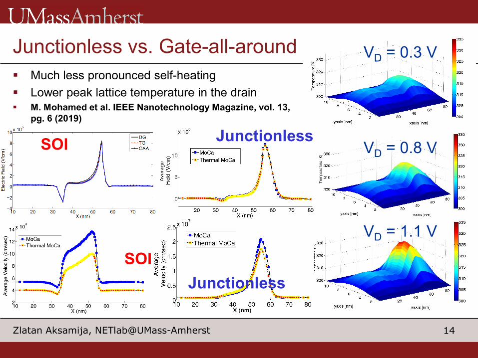
Junctionless vs. Gate-all-around Much less pronounced self-heating Lower peak lattice temperature in the drain M. Mohamed et al. IEEE Nanotechnology Magazine, vol. 13,
pg. 6 (2019)
VD = 0.8 V
VD = 1.1 V
VD = 0.3 V
SOI Junctionless
SOIJunctionless
15Zlatan Aksamija, NETlab@UMass-Amherst
Thermoelectric Energy Conversion Semiconductor nanostructures are efficient thermo-electric converters:
remove or recycle all that waste heat!
C. J. Vineis et al., Adv. Mat. 22, 3970-3980 (2010)L. E. Bell, Science vol. 321, pp. 1457-1461 (2008)
16Zlatan Aksamija, NETlab@UMass-Amherst
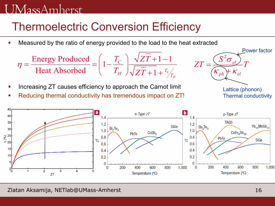
Thermoelectric Conversion Efficiency Measured by the ratio of energy provided to the load to the heat extracted
Increasing ZT causes efficiency to approach the Carnot limit Reducing thermal conductivity has tremendous impact on ZT!
Energy Produced 1 11Heat Absorbed 1 C
H
C
TH T
T ZTT ZT
η + −
= = − + +
TSZTelph
el
κκσ+
=2
Power factor
Lattice (phonon)Thermal conductivity
17Zlatan Aksamija, NETlab@UMass-Amherst
Thermoelectric Applications• Car Exhaust Systems• Wearable Electronics• Solar-Thermal Generators• Nanoscale Power Sources
G. J. Snyder, ECS Interface, pp. 54, Fall 2008
18Zlatan Aksamija, NETlab@UMass-Amherst
Nanoscale Phonon Transport Overview
H. J. Ryu, Z. Aksamija, et al., Phys. Rev. Lett. 105, 256601 (2010)
C. J. Vineis et al., Adv. Mater. 22, 3970 (2010)
19Zlatan Aksamija, NETlab@UMass-Amherst
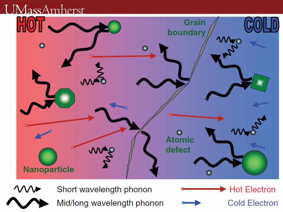
Bouondary/Interface Scattering of Phonons
Nanostructures have lots of interfaces! At a rough interface, phonons can be either
reflected or scattered
If the phonon is large (or surface smooth)• The surface variations look small• ReflectionNo change in momentum
Typical phonon is small (wavelength<roughness)• The surface variation looks big!• Scattered randomlyResistance!
Momentum-dependent specularity:
20Zlatan Aksamija, NETlab@UMass-Amherst
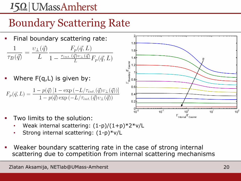
Boundary Scattering Rate Final boundary scattering rate:
Where F(q,L) is given by:
Two limits to the solution:• Weak internal scattering: (1-p)/(1+p)*2*v/L• Strong internal scattering: (1-p)*v/L
Weaker boundary scattering rate in the case of strong internal scattering due to competition from internal scattering mechanisms
21Zlatan Aksamija, NETlab@UMass-Amherst
Ultrathin SOI thermal conductivity anisotropy Lowest thermal conductivity on a (001), highest on (011) surface
Z. Aksamija and I. Knezevic, Phys. Rev. B 82, 045319 (2010)
Ratio of highest/lowest in-plane conductivity a factor of >2 at room temp., increases with roughness
in-plane
out-of-plane
22Zlatan Aksamija, NETlab@UMass-Amherst
Phonons, Dispersion, and Focusing Phonon isosurfaces show strong anisotropy and phonon
focusing [Cahill et al., JAP 93, 793 (2003)] LA branch (left) has very flat faces with phonons propagating
mainly in the [111] direction TA branch (middle) has flat isosurfaces with normal vectors
(phonon velocities) in the [100] direction
Phonon Dispersion
Longitudinal
Transverse
Acoustic (propagating waves)
Optical (standing waves)
Z. Aksamija and I. Knezevic, Phys. Rev. B 82, 045319 (2010)
Superlattices are made up from many thin (few nm) layers of alternating semiconductor materials
Layers separated by a rough interface with an rms roughness Δ Thermal conductivity of the two alternating layers is combined in series for
cross-plane transport and in parallel for in-plane transport
Additional interface resistance due to acousticmismatch between dissimilar materials
24Zlatan Aksamija, NETlab@UMass-Amherst
Anisotropic thermal conductivity in SiGe alloy SLs Strong in-plane/cross-plane anisotropy in 4 nm period Si/Ge SL Very low (1~5 W/m/K) cross-plane (through the SL) lattice thermal conductivity
in Si/Ge SLs with a wide range of period thickensses (right) Thermal conductivity below alloy limit in SiGe alloy SLs!
Data points from: Liu et al., J. Nanosci. Nanotech. 1, 39 (2001) Data points from: Lee et al., Appl. Phys. Lett. 70, 2957 (1997)Data from: Huxtable et al. Appl. Phys. Lett. 80, 1737 (2001) Theory: Aksamija and Knezevic, Phys. Rev. B 88, 155318 (2013)
25Zlatan Aksamija, NETlab@UMass-Amherst
Thermal conductivity in nanocomposites Nanocomposites are cheaper to make than SLs More difficult problem due to random grain structure
Nature Materials 3, 668 - 669 (2004)
Tadjer et al., IEEE EDL 33, 23-25 (2012)
Diam. Rel. Mat. 18, 1043 (2009)
26Zlatan Aksamija, NETlab@UMass-Amherst
Simulation of thermal transport in nanocomposites Pick the grain size from the Voronoi diagram and
compute diameter Compute the full thermal conductivity tensor
of each grain:
Network of “resistors” based on nearest neighbors Distance and thermal conductivity of each grain Iterate the heat current until convergence:
Z. Aksamija, J. Elec. Mater. Vol. 44, pp. 1644-1650 (2015)
27Zlatan Aksamija, NETlab@UMass-Amherst
Phonon Monte Carlo and the Boltzmann eqn. Solve the phonon Boltzmann transport equation:
• Motion
• Scattering
7-dimensional (3+3 phase space + time)use MC technique Top eqn. is the classical equation of motion Bottom is the collision integral from quantum-mechanical
perturbation theory (Fermi’s Golden Rule) Sample scattering probability at
random from Poisson process:
( ) ( ) ( )
( ) ( )
.
.
,,
( , ) , ( , ) ,
rkscat
kscat
n r q dnq n r qt dt
dn P q q n r q P q q n r qdt
λλλ
λ λ
ω
′
∂ +∇ ∇ = ∂
′ ′ ′ = − − ∑
q
28Zlatan Aksamija, NETlab@UMass-Amherst
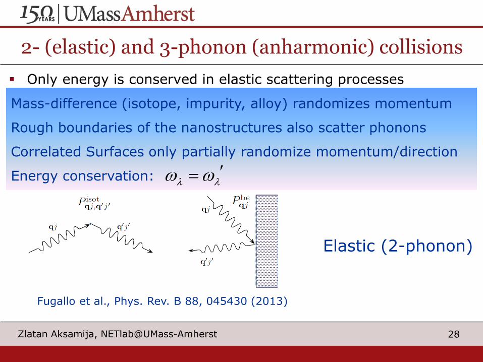
Elastic (2-phonon)
Inelastic (3-phonon)
Fugallo et al., Phys. Rev. B 88, 045430 (2013)
2- (elastic) and 3-phonon (anharmonic) collisions Only energy is conserved in elastic scattering processes
Rough boundaries of the nanostructures also scatter phonons
Correlated Surfaces only partially randomize momentum/direction
Energy conservation: λ λω ω ′=
29Zlatan Aksamija, NETlab@UMass-Amherst
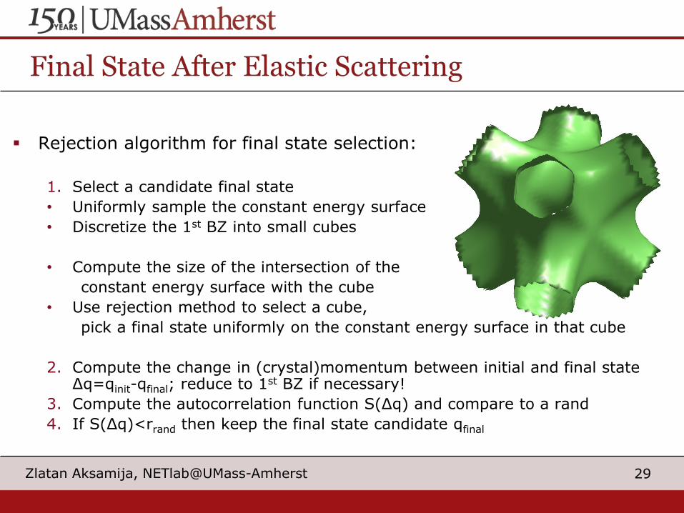
Final State After Elastic Scattering
Rejection algorithm for final state selection:
1. Select a candidate final state• Uniformly sample the constant energy surface• Discretize the 1st BZ into small cubes
• Compute the size of the intersection of the constant energy surface with the cube
• Use rejection method to select a cube, pick a final state uniformly on the constant energy surface in that cube
2. Compute the change in (crystal)momentum between initial and final state Δq=qinit-qfinal; reduce to 1st BZ if necessary!
3. Compute the autocorrelation function S(Δq) and compare to a rand4. If S(Δq)<rrand then keep the final state candidate qfinal
30Zlatan Aksamija, NETlab@UMass-Amherst
Elastic (2-phonon)
Fugallo et al., Phys. Rev. B 88, 045430 (2013)
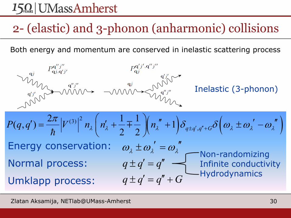
2- (elastic) and 3-phonon (anharmonic) collisions
Both energy and momentum are conserved in inelastic scattering process
Energy conservation:
Normal process:
Umklapp process:
( ) ( )2(3),
2 1 1( , ) 12 2 q q q GP q q V n n nλ λ λ λ λ λ
π δ δ ω ω ω′ ′′± + ′′ ′ ′′′ ′= + + ± −
q q qq q q G
λ λ λω ω ω′ ′′± =′ ′′± =′ ′′± = +
Non-randomizingInfinite conductivityHydrodynamics
Inelastic (3-phonon)
31Zlatan Aksamija, NETlab@UMass-Amherst
Superdiffusive phonons in Si-Ge alloysSi SiGe
The distance along the NW traveled by a phonon between scattering events Si NWs have a more uniform distribution characteristic of the dominance of diffuse
boundary scattering with a white-noise-like appearance Phonon flights in SiGe NWs are comprised of short flights interrupted by long leaps
Blue line – individual distance/time Red line – cumulative distance/time
V. Zaburdaev, et al., Lévy walks. Rev. Mod. Phys., 87:483–530, 2015.
32Zlatan Aksamija, NETlab@UMass-Amherst
Length scaling in Si-Ge NWs
Histogram of the flight lengths in Si(red) and SiGe NWs (blue). The broadspectrum of MFPs in SiGe NWs leadsto a heavy-tailed distribution.
Heavy Tail
33Zlatan Aksamija, NETlab@UMass-Amherst
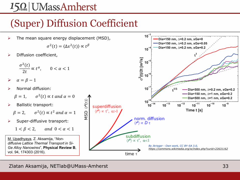
(Super) Diffusion Coefficient
Diffusion coefficient,
𝜎𝜎2 𝑡𝑡2𝑡𝑡
∝ 𝑡𝑡𝛼𝛼, 0 < 𝛼𝛼 < 1
𝛼𝛼 = 𝛽𝛽 − 1
Normal diffusion:
𝛽𝛽 = 1, 𝜎𝜎2 𝑡𝑡 ∝ 𝑡𝑡 𝑎𝑎𝑎𝑎𝑎𝑎 𝛼𝛼 = 0
Ballistic transport:
𝛽𝛽 = 2, 𝜎𝜎2 𝑡𝑡 ∝ 𝑡𝑡2 𝑎𝑎𝑎𝑎𝑎𝑎 𝛼𝛼 = 1
Super-diffusive transport:
1 < 𝛽𝛽 < 2, 𝑎𝑎𝑎𝑎𝑎𝑎 0 < 𝛼𝛼 < 1
The mean square energy displacement (MSD),
𝜎𝜎2 𝑡𝑡 = Δ𝑥𝑥2(𝑡𝑡) ∝ 𝑡𝑡𝛽𝛽
By Jkrieger - Own work, CC BY-SA 3.0,https://commons.wikimedia.org/w/index.php?curid=22631162
M. Upadhyaya, Z. Aksamija, “Non-diffusive Lattice Thermal Transport in Si-Ge Alloy Nanowires”, Physical Review B, vol. 94, 174303 (2016).