NTT Technical Review 31 Vol. 18 No. 10 Oct. 2020 1. Optical technology: from communication to processing Optical technology is currently the driving force behind large-capacity information transmission including long-haul optical fiber communication and inter-server communication in datacenters. By exten- sion, progress in optical communication for shorter distances can be considered but will ultimately mean optical networking on a computer chip and informa- tion processing based directly on light. Developing an optical computer has been one of the major goals of researchers in the field of optics, but the mature complementary metal-oxide semiconductor (CMOS) electronic circuit technology has prevented any meaning from being found in using light in comput- ing. However, CMOS-based nano-fabrication and circuit integration are gradually approaching their limits, so expectations are increasing for information processing using the high-speed properties of light [1]. These expectations are being boosted by progress in miniature and energy-saving optical device and circuit technology made possible by fine-processing technology called nanophotonics. Recent advances in silicon photonics technology are also generating strong synergy with nanophotonics, and the imple- mentation of a large-scale optical circuit in a compact space is expanding the opportunities for photonic computing research. Though it is generally difficult to carry out various types of information processing solely with optical circuits, importance is being given to an accelerator that can accelerate specific processing by combining optical circuits with the parallel digital processor and large-capacity memory of CMOS electronics and enabling optical circuits to carry out high-speed-spe- cific processing applicable to light [2]. In particular, the value of using light has been reevaluated recently as extending beyond digital processing to include analog processing as in machine learning and pho- tonic microwave-signal processing, and an opto- electronic integrated accelerator that links CMOS electronics and nanophotonics has begun to take form. The following introduces a low-latency optical pass-gate circuit, opto-electronic converters, and an optical nonlinear device as three key components deemed essential to developing an opto-electronic integrated accelerator (Fig. 1). Nanophotonic Technologies toward Opto-electronic Integrated Accelerators Kengo Nozaki, Akihiko Shinya, and Masaya Notomi Abstract The opto-electronic integration technology being researched at the NTT Nanophotonics Center is for creating a photonic computing platform with low latency and low energy consumption. The development of miniature optical functional devices through nanophotonics along with advances in large-scale opti- cal-circuit fabrication technology will make diverse types of photonic-information processing possible. This article introduces the technologies that we are researching for optical pass-gate circuits, opto- electronic converters, and optical nonlinear devices and presents the path to opto-electronic integrated accelerators that the combined use of these technologies will make possible. Keywords: opto-electronic integration, photonic computing, photonic crystal Feature Articles: Photonics-electronics Convergence Technology to Achieve All-Photonics Network
Transcript
NTT Technical Review 31Vol. 18 No. 10 Oct. 2020
1. Optical technology: from communication to processing
Optical technology is currently the driving force behind large-capacity information transmission including long-haul optical fiber communication and inter-server communication in datacenters. By exten-sion, progress in optical communication for shorter distances can be considered but will ultimately mean optical networking on a computer chip and informa-tion processing based directly on light. Developing an optical computer has been one of the major goals of researchers in the field of optics, but the mature complementary metal-oxide semiconductor (CMOS) electronic circuit technology has prevented any meaning from being found in using light in comput-ing. However, CMOS-based nano-fabrication and circuit integration are gradually approaching their limits, so expectations are increasing for information processing using the high-speed properties of light [1]. These expectations are being boosted by progress in miniature and energy-saving optical device and circuit technology made possible by fine-processing technology called nanophotonics. Recent advances in silicon photonics technology are also generating
strong synergy with nanophotonics, and the imple-mentation of a large-scale optical circuit in a compact space is expanding the opportunities for photonic computing research.
Though it is generally difficult to carry out various types of information processing solely with optical circuits, importance is being given to an accelerator that can accelerate specific processing by combining optical circuits with the parallel digital processor and large-capacity memory of CMOS electronics and enabling optical circuits to carry out high-speed-spe-cific processing applicable to light [2]. In particular, the value of using light has been reevaluated recently as extending beyond digital processing to include analog processing as in machine learning and pho-tonic microwave-signal processing, and an opto-electronic integrated accelerator that links CMOS electronics and nanophotonics has begun to take form.
The following introduces a low-latency optical pass-gate circuit, opto-electronic converters, and an optical nonlinear device as three key components deemed essential to developing an opto-electronic integrated accelerator (Fig. 1).
AbstractThe opto-electronic integration technology being researched at the NTT Nanophotonics Center is for
creating a photonic computing platform with low latency and low energy consumption. The development of miniature optical functional devices through nanophotonics along with advances in large-scale opti-cal-circuit fabrication technology will make diverse types of photonic-information processing possible. This article introduces the technologies that we are researching for optical pass-gate circuits, opto-electronic converters, and optical nonlinear devices and presents the path to opto-electronic integrated accelerators that the combined use of these technologies will make possible.
Feature Articles: Photonics-electronics Convergence Technology to Achieve All-Photonics Network
Feature Articles
32NTT Technical Review Vol. 18 No. 10 Oct. 2020
2. Low-latency optical pass-gate circuit
The barrier to the continuation of Moore’s law in CMOS electronic circuits (empirical rule stating that performance improves due to finer processing and greater integration) is the increase in signal delay and heat generation as a result of resistance and capaci-tance of transistors and metal wiring. In electronic circuits, digital logic operations, such as AND-OR-INVERT logic, are carried out by cascaded connec-tion of logic gates. A subsequent gate waits for the signal output from a prior gate so that the time delay to obtain the calculation result increases proportion-ally to the number of gate stages. In addition, increas-ing the signal bit rate increases heat generation due to an increase in the movement of free electrons in metal. As a consequence, the signal bit rate of CMOS electronics for computing that requires low power consumption has generally been held to several giga-hertz. For these reasons, the current situation is that, while processing capacity (throughput) can be increased through further increases in CMOS fine processing and integration, processing delay (laten-cy) is hitting a ceiling.
As shown in Fig. 2, an optical pass-gate circuit consists of the integration of optical switches that switch optical transmission paths. In the example shown in Fig. 2(a), calculation results are output by
triggering Mach-Zehnder interferometer optical switches* at the same time by signals from the elec-tronic circuit and transmitting light along the selected paths as light beams interfere with each other. There is no power loss or heat generation due to resistance, as in the case of electronic circuits, and calculations are carried out through the interference of light, which opens the door to low-energy and low-latency processing. We can take as an example a full-adder circuit that inputs digital signals (“1” and “0” binary signals). The calculation of the carry signal from least-significant bit to most-significant bit constitutes the adder’s critical path that determines total delay. However, carrying out such processing using optical pass-gates is expected to reduce delay compared with that of electronic circuits [3]. Therefore, optical pass-gates should be applicable to other digital operations including basic arithmetic operations.
In addition to digital processing, progress is also being made in analog processing (carried out with continuous values). In particular, there are high
Fig. 1. Conceptual schematic of an opto-electronic integrated accelerator.
Optical nonlineardevice
Opto-electronicconverters
This circuit carries out low-latency operationprocessing using light propagation. Itimplements optical digital logic, optical microwave processing, optical neuralnetworks, etc.
CMOSelectronicprocessor
These devices carry out mutual conversion ofoptical and electrical signals, therefore actingas an interface between the CMOS electroniccircuit and optical circuit.
This device amplifies and applies nonlinearfunctions to input optical signals andtransfers as output. It is used for increasingthe scale of optical circuits or carrying outnonlinear optical processing.
Optical pass-gatecircuit
* Mach-Zehnder interferometer optical switch: A switch that splits light into two beams and applies voltage to one, thereby changing the refractive index of that waveguide and changing the phase of light. It then determines the light output by having the two light beams interfere with each other (see Fig. 2). Digital processing determines the output ratio to be either 0/1 or 1/0, while analog processing results in a continuous output ratio from 0 to 1.
Feature Articles
NTT Technical Review 33Vol. 18 No. 10 Oct. 2020
expectations for microwave photonics technology to convert microwave signals used in wireless commu-nications to light, execute processing that requires high spectral resolution and temporal resolution (fil-tering, waveform control, dispersion control, etc.) in the optical domain, and output the results again as microwave signals (Fig. 2(b)) [4]. At the same time, research on optical neural networks is becoming quite active worldwide along with advances in deep learning and other artificial intelligence technologies. At the core of this analog processing is vector-matrix multiplication (VMM), but its calculation cost has been a bottleneck in CMOS digital circuits. On the other hand, a pass-gate circuit based on light interface can be used to physically implement VMM, so a solu-tion to these problems is expected [5]. The possibility exists of achieving low-latency inference by combin-ing this optical pass-gate circuit with an opto-elec-tronic converter and optical nonlinear device, as
described below, to configure opto-electronic neural network integration (Fig. 2(c)).
3. Opto-electronic converters (interface between optical and electronic circuits)
A major issue in integrating CMOS and optical circuits is developing a high-density opto-electronic interface featuring a miniature and energy-saving electrical-to-optical (E-O) converter, i.e. an electro-optic modulator (EOM), and optical-to-electrical (O-E) converter, i.e. a photodetector (PD). We have been developing such converters using nanostruc-tures called photonic crystals (Fig. 3), which are periodic structures formed in semiconductors. They can be used as ultrasmall optical waveguides and optical resonators by forming periodic airholes with diameters of ~200 nm on a thin semiconductor plate and arranging their layout. At NTT, we developed
Fig. 2. Example of optical pass-gate circuits: (a) optical digital logic processing, (b) optical microwave processing, (c) optical neural network.
Pseudo digital outputHigh-speed E-O converter High-speed O-E converter
Light
Photonic layer
110..101..
010.. 111..
101..
001..
(b)
Weight voltage controller
Inference: “8”
Optical data
(c)
Feature Articles
34NTT Technical Review Vol. 18 No. 10 Oct. 2020
functional devices such as optical switches, optical memory, and laser sources and demonstrated record-low energy operation. We also demonstrated E-O and O-E converters, i.e., a nanophotonic EOM and PD, as shown in Figs. 3(a) and (b), and succeeded in dra-matically reducing the size and energy consumption of these converters compared with those of conven-tional ones [6].
For E-O/O-E converters, the low electrical capaci-tance can be an important figure of merit. As shown in Fig. 3(c), the capacitance of a single CMOS tran-sistor is less than one femtofarad (fF), whereas that of conventional E-O/O-E converters is generally large, i.e., 10 fF or greater. This requires high energy con-sumption in proportion to the large capacitance, cre-ating a bottleneck. On the other hand, our converters can reduce capacitance to less than 1 fF, the same as
that of CMOS transistors. Such a capacitance reduc-tion is of major significance. As shown in Fig. 3(d), optical communication based on conventional E-O/O-E converters requires multiple amplifier stag-es to generate a sufficient voltage signal, which increases power consumption and device area. In contrast, the electrical energy required for logic operations in CMOS transistors can be sufficient to drive our low-capacitance converters, enabling seam-less opto-electronic integration requiring no amplifi-ers. We therefore expect our converters to be used for configuring dense optical networks either between or within CMOS chips based on simple optical trans-ceiver circuits with a strong energy-saving effect and for even optical-signal processing within communi-cation. Going forward, the key to these advances is integrating CMOS and opto-electronic converters
Fig. 3. Performances of opto-electronic converters using photonic crystals: (a) nanophotonic EOM, (b) nanophotonic PD, (c) comparison of device capacitance, and (d) simplification of optical communication circuit with low-capacitance opto-electronic converters.
InGaAsP: indium gallium arsenide phosphide
(a)
(c) (d)
Optical transmission with generalopto-electronic converters
Optical transmission with low-capacitanceopto-electronic converters
(b)
Photonic crystal (periodic airholes)
p-i-n junction
Embedded InGaAs light absorber
Photonic-crystal nano-resonator
Optical signal
Continuous light Optical signal
Long-haul opticalcommunications
(> 100 fF)Silicon photonics
(~10 fF)
Current optical technology
Photonic-crystalopto-electronic
converters (< 1 fF)
(Large optical loss) Plasmonics
Electronics technology
CMOS transistorgate (< 1 fF)
Transmission
Embedded InGaAsPnonlinear layer
• Device area < 10 µm2
• Operation voltage = 0.5 V• Energy consumption < 0.1 fJ/bit• Operation bitrate = 40 Gbit/s
• Device area < 10 µm2
• Optical responsivity = 1 A/W• Energy consumption = several fJ/bit• Noise equivalent power < 1 pW/Hz0.5
• Operation bitrate > 10 Gbit/s
Current optical technology:Capacitance is too large toconnect with CMOS transistors
Optical transmitter
Amplifiers10 aF 100 aF 1 fF 10 fF 100 fF 1 pF
Inputvoltage(> 3 V)
Inputvoltage
(< 0.5 V)Outputvoltage
(> 0.5 V)
Amplifiers
Outputvoltage
(> 0.5 V)
PhotoreceiverCapacitance (F: farad)
Transmission +
(Processing)
Feature Articles
NTT Technical Review 35Vol. 18 No. 10 Oct. 2020
while maintaining low capacitance and developing opto-electronic interfaces toward practical comput-ing applications.
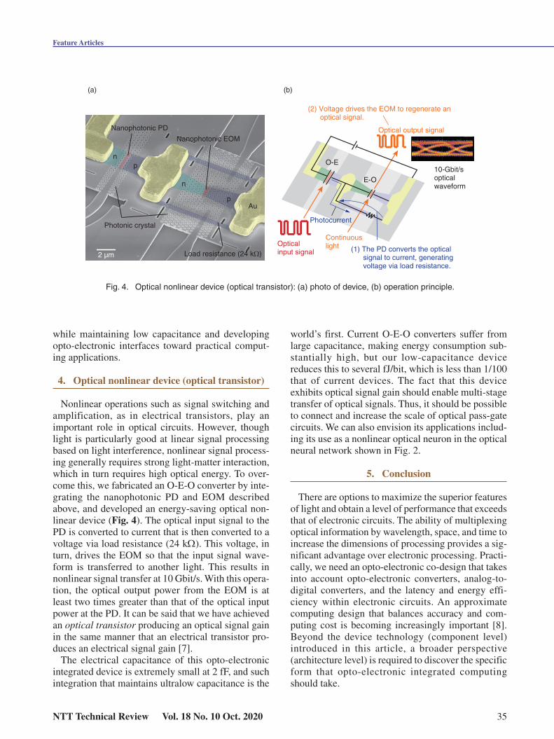
4. Optical nonlinear device (optical transistor)
Nonlinear operations such as signal switching and amplification, as in electrical transistors, play an important role in optical circuits. However, though light is particularly good at linear signal processing based on light interference, nonlinear signal process-ing generally requires strong light-matter interaction, which in turn requires high optical energy. To over-come this, we fabricated an O-E-O converter by inte-grating the nanophotonic PD and EOM described above, and developed an energy-saving optical non-linear device (Fig. 4). The optical input signal to the PD is converted to current that is then converted to a voltage via load resistance (24 kΩ). This voltage, in turn, drives the EOM so that the input signal wave-form is transferred to another light. This results in nonlinear signal transfer at 10 Gbit/s. With this opera-tion, the optical output power from the EOM is at least two times greater than that of the optical input power at the PD. It can be said that we have achieved an optical transistor producing an optical signal gain in the same manner that an electrical transistor pro-duces an electrical signal gain [7].
The electrical capacitance of this opto-electronic integrated device is extremely small at 2 fF, and such integration that maintains ultralow capacitance is the
world’s first. Current O-E-O converters suffer from large capacitance, making energy consumption sub-stantially high, but our low-capacitance device reduces this to several fJ/bit, which is less than 1/100 that of current devices. The fact that this device exhibits optical signal gain should enable multi-stage transfer of optical signals. Thus, it should be possible to connect and increase the scale of optical pass-gate circuits. We can also envision its applications includ-ing its use as a nonlinear optical neuron in the optical neural network shown in Fig. 2.
5. Conclusion
There are options to maximize the superior features of light and obtain a level of performance that exceeds that of electronic circuits. The ability of multiplexing optical information by wavelength, space, and time to increase the dimensions of processing provides a sig-nificant advantage over electronic processing. Practi-cally, we need an opto-electronic co-design that takes into account opto-electronic converters, analog-to-digital converters, and the latency and energy effi-ciency within electronic circuits. An approximate computing design that balances accuracy and com-puting cost is becoming increasingly important [8]. Beyond the device technology (component level) introduced in this article, a broader perspective (architecture level) is required to discover the specific form that opto-electronic integrated computing should take.
[2] K. Kitayama, M. Notomi, M. Naruse, K. Inoue, S. Kawakami, and A. Uchida, “Novel Frontier of Photonics for Data Processing—Photonic Accelerator,” APL Photonics, Vol. 4, 090901, 2019.
[3] A. Shinya, T. Ishihara, K. Inoue, K. Nozaki, and M. Notomi, “Ultralow-latency Optical Circuit Based on Optical Pass-gate Logic,” NTT Technical Review, Vol. 16, No. 7, pp. 8–13, 2018.
[4] D. Perez, I. Gasulla, and J. Capmany, “Programmable Multifunc-tional Integrated Nanophotonics,” Nanophotonics, Vol. 7, No. 8, pp. 1351–1371, 2018.
[5] Y. C. Shen, N. C. Harris, S. Skirlo, M. Prabhu, T. Baehr-Jones, M.
Hochberg, X. Sun, S. J. Zhao, H. Larochelle, D. Englund, and M. Soljacic, “Deep Learning with Coherent Nanophotonic Circuits,” Nature Photonics, Vol. 11, pp. 441–446, 2017.
[6] K. Nozaki, S. Matsuo, T. Fujii, K. Takeda, E. Kuramochi, A Shinya, and M. Notomi, “Ultralow-capacitance Optoelectronic Converters Using a Photonic Crystal,” NTT Technical Review, Vol. 16, No. 7, pp. 8–13, 2018.
[7] K. Nozaki, S. Matsuo, T. Fujii, K. Takeda, A. Shinya, E. Kuramochi, and M. Notomi, “Femtofarad Opto-electronic Integration Demon-strating Energy-saving Signal Conversion and Nonlinear Functions,” Nature Photonics, Vol. 13, pp. 454–459, 2019.
[8] S. Kawakami, T. Tanimoto, S. Kita, A. Shinya, T. Ono, M. Notomi, and K. Inoue, “Power-performance Modeling and Potential Analysis of VMM Based Approximate Optical Computing,” Information Pro-cessing Society of Japan (IPSJ) SIG Technical Reports, 2019-ARC-237, pp. 1–8, 2019.
structure Research Group of NTT Basic Research Laboratories and NTT Nanophotonics Center.
He received a B.E., M.E., and Ph.D. in electri-cal engineering from Yokohama National Uni-versity, Kanagawa, in 2003, 2005, and 2007. He joined NTT Basic Research Laboratories in 2008. His current interests are ultralow-power nanophotonic semiconductor devices based on photonic crystals. He received the Best Paper Award at Photonics in Switching 2012, the Young Researchers Award from the Institute of Elec-tronics, Information and Communication Engi-neers (IEICE) Lasers and Quantum Electronics in 2014, the Best Paper Award from OptoElec-tronics and Communications Conference)/ Inter-national Conference on Photonics in Switching (OECC/PS) in 2016, and the Commendation for Science and Technology by the Minister of Edu-cation, Culture, Sports, Science and Technology of Japan (the Young Scientists’ Prize) in 2019. He is a member of the Japan Society of Applied Physics (JSAP).
Nanostructure Research Group of NTT Basic Research Laboratories. Project leader of NTT Nanophotonics Center.
He received a B.E., M.E., and Ph.D. in applied physics from the University of Tokyo in 1986, 1988, and 1997. He joined NTT in 1988, where his research has focused on controlling the opti-cal properties of materials/devices by using arti-ficial nanostructures (quantum wires/dots and photonic crystals). In addition to his work at NTT, he has also been a professor at the Depart-ment of Physics, Tokyo Institute of Technology since 2017. He received the IEEE/LEOS Distin-guished Lecturer Award (2006) from the Institute of Electrical and Electronics Engineers/Lasers & Electro-Optics Society, the JSPS prize (2009) from the Japan Society for the Promotion of Sci-ence, a Japan Academy Medal (2009), and the Commendation for Science and Technology by the Minister of Education, Culture, Sports, Sci-ence and Technology of Japan (2010). He is serving as a member of National University Corporation Evaluation Committee in the Japa-nese government. He is an IEEE Fellow and a member of JSAP, the American Physical Society, and the Optical Society (OSA).
Akihiko ShinyaGroup Leader, Senior Research Scientist,
Supervisor, Photonic Nanostructure Research Group of NTT Basic Research Laboratories and NTT Nanophotonics Center.
He received a B.E., M.E., and Ph.D. in electri-cal engineering from Tokushima University in 1994, 1996, and 1999. In 1999, he joined NTT Basic Research Laboratories. He has been engaged in research and development of photon-ic-crystal devices. He is a member of JSAP and the Laser Society of Japan.


![LACUNARITY PROPERTIES OF NANOPHOTONIC MATERIALS BASED …mit.imt.si/Revija/izvodi/mit171/tomic.pdf · m. tomi] et al.: lacunarity properties of nanophotonic materials based on ...](https://static.documents.pub/doc/80x56/5c77329109d3f2cd0e8b6949/lacunarity-properties-of-nanophotonic-materials-based-mitimtsirevijaizvodimit171tomicpdf.jpg)
