THESIS FOR THE DEGREE OF DOCTOR OF ENGINEERING Nanoplasmonic Alloy Hydrogen Sensors A Quest for Fast, Sensitive and Poisoning- Resistant Hydrogen Detection FERRY ANGGORO ARDY NUGROHO Department of Physics CHALMERS UNIVERSITY OF TECHNOLOGY Gothenburg, Sweden 2018
Transcript
THESIS FOR THE DEGREE OF DOCTOR OF ENGINEERING
Nanoplasmonic Alloy Hydrogen
Sensors
A Quest for Fast, Sensitive and Poisoning-
Resistant Hydrogen Detection
FERRY ANGGORO ARDY NUGROHO
Department of Physics
CHALMERS UNIVERSITY OF TECHNOLOGY
Gothenburg, Sweden 2018
ii
Nanoplasmonic Alloy Hydrogen Sensors
A Quest for Fast, Sensitive and Poisoning-Resistant Hydrogen Detection
1.3 Gas Sensors for Environmental Sustainability The overarching goal of the hydrogen economy is to create a sustainable environment through
the use of hydrogen as a sustainable energy carrier. A loose definition of a sustainable
environment used here is when our ecosystem (i.e. our lovely earth) is able to maintain its ability
to provide its natural resources upon which we critically depend. Unfortunately, industrial
revolution that began more than a century ago brought with it the release of unnatural amounts
of polluting gases that disturb the balance of our environment. This is clearly reflected in global
warming (caused specifically by the so-called greenhouse gases CO2, CH4, NO2 and O3) whose
consequences includes e.g. rising sea levels and weather anomalies. In fact, global warming,
along with the creation of a sustainable energy system, are two of society’s grandest challenges
in the 21st century.62 Thus, in line with the goals behind the hydrogen economy, complementary
action to monitor, control and finally reduce the emission of polluting gases is necessary. This
creates a need for development of highly selective gas sensors for species beyond H2, i.e. CO2,
CO, NO2. Beyond the traditional purpose of simple “detection” of a species, a sensor can also
serve as a means to assess characteristics of materials, for example how they “interact” with
gas species. As a minor part of this thesis, I thus also explore the possibility of using
nanoplasmonic sensors as an analytical tool to assess the CO2 sorption properties of mesoporous
materials.
1.3.1 Carbon Capture and Storage
Anthropogenic CO2 emissions (i.e. the ones originating from human activity through e.g. fossil
fuel combustion and industrial processes) constitute 65% of global greenhouse gases, and CO2
has been pinned down as the gas most responsible for the global warming effect.62,63 At the
individual level, CO2 pollution may cause an excessive amount of CO2 in the blood, which
typically results in a serious and sometimes fatal condition characterized by headache, nausea
and visual disturbances.64,65 Therefore, numerous mitigation strategies for CO2 emission
reduction are suggested or actively being applied. One particular direction is the Carbon
Capture and Storage (CCS) scheme whose goal is to capture waste CO2 from large point
sources (e.g. fossil fuel power plants or concrete factories), transport it to a storage site and
deposit it where it will not enter the atmosphere (or reuse it in a considerable amount for other
industrial processes).
The successful deployment of CCS schemes requires close collaboration between different
fields, ranging from politics to technology. One of the consequences of the increasing interest
in CCS in the technological field is the accelerated search for materials that can capture CO2.
Numerous kinds of materials have been reported and used: e.g. (liquid) amines, metal oxides,
8
zeolites, metal-organic frameworks (MOFs) and polymers.66–71 The last three of the mentioned
examples belong to the class of mesoporous materials, which are attractive for CCS due to their
very high specific surface area (the current record for the highest specific surface area for porous
material is held by NU-109 and NU-110. Both belong to a class of MOF, whose surface area
reaches 7000 m2/g; that is, one kilogram of the material contains an internal surface area that
could cover seven square kilometers!72). However, despite the made progress in the field, the
development of cheap, scalable and environmentally friendly CO2 sorbents is still highly
desired.
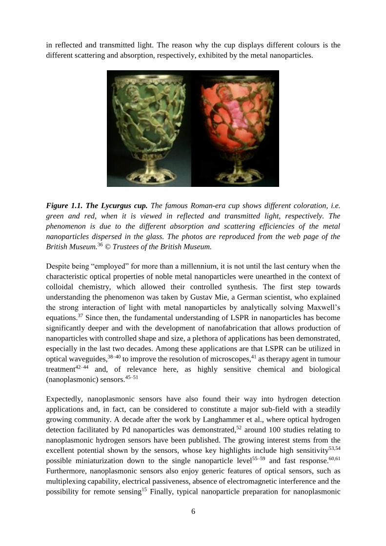
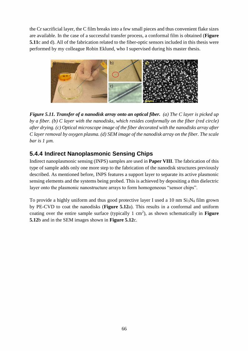
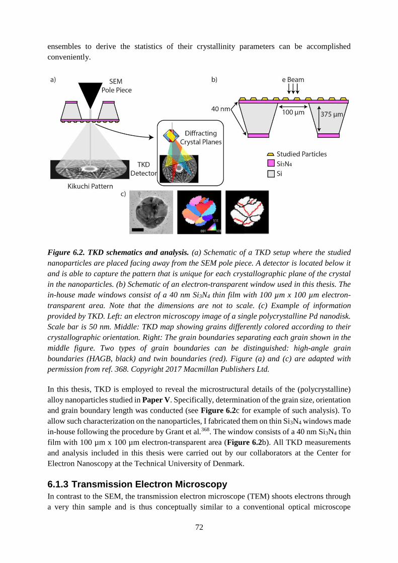
Figure 1.4. Carbon Capture and Storage. Carbon Capture and Storage (CCS) is the process
of capturing waste CO2 from large point sources (e.g. fossil fuel power plant or concrete
factory), transporting it to a storage site, and depositing it where it will not enter the
atmosphere, normally an underground geological formation. One of the ways to capture the
CO2 is by utilizing sorbent materials that are able to selectively adsorb the CO2 from gas
mixtures. The interaction strength of CO2 with the sorbent materials is expressed through the
isosteric heat of adsorption (Qst). Some of the icons used in the schematic are taken from a
webpage.13
Capture of CO2 with these materials is based on the idea that CO2 selectively adsorbs from gas
mixtures and can be recovered as nearly pure CO2 by cyclically increasing the temperature or
decreasing the pressure.66,73 For successful CO2 capture (and release), the CO2-adsorbent
interaction strength should be engineered in an optimal way.74 It should be strong enough so
that CO2 cannot easily escape at conditions characteristic for the environment from which it is
to be removed (in other words, these conditions can vary greatly for specific applications) but
also not too strong so that complete release can be achieved by mild heating to make the process
energy efficient.
The interaction strength of CO2 with a sorbent is typically assessed by measuring the isosteric
heat of adsorption (Qst) using various methods based on gravimetric and volumetric
measurement principles. Gravimetric techniques are complicated by buoyancy and Knudsen
9
diffusion at low pressure, while volumetric techniques need accurate dead space volume
determination for correction. Furthermore, both methods have a common requirement for
accurate determination of sample initial weight and/or volume.75 Additionally, porous polymer
systems (as well as, e.g., MOFs) potentially show swelling upon CO2 adsorption, which further
complicates their analysis.76 Therefore it is very appealing to develop new experimental
strategies for the scrutiny of CO2 sorption processes in such materials. Ideally, the experimental
methodology developed is generic, easy to use, accurate, and allows rapid characterization for
efficient screening of new materials for CCS. Using indirect nanoplasmonic sensing, I
demonstrate in Paper VIII that optical spectroscopy based on plasmonics is suitable for the
aforementioned purposes.
1.4 This Thesis This thesis comprises work related to developing and establishing nanoplasmonic materials and
structures as hydrogen sensors. Specifically, in this thesis I introduce nanoalloys as a new class
of transducing materials to be used in such sensors with the ambition that it can be the platform
that is able to satisfy all of the hydrogen sensing metric requirements outlined in Table 1.1. In
order to do so, the work undertaken in this thesis constitutes a coherent effort to reach this goal.
At the heart of this effort is the first part of my work, where I demonstrate a bottom-up
nanofabrication method to create alloy nanoparticle arrays for plasmonic applications in
general, and for hydrogen sensing in particular (Paper I). Having established this base, and
before taking the discussion to the level of the performance of alloy nanoparticles as hydrogen
sensors, it was then of importance to establish the correlation between the generated optical
signal of an alloy nanoplasmonic sensor and the hydrogen concentration inside the
nanoparticles. Therefore, in Paper II, I scrutinize this correlation by establishing a combined
gravimetric and optical experimental setup that enabled simultaneous measurement of the
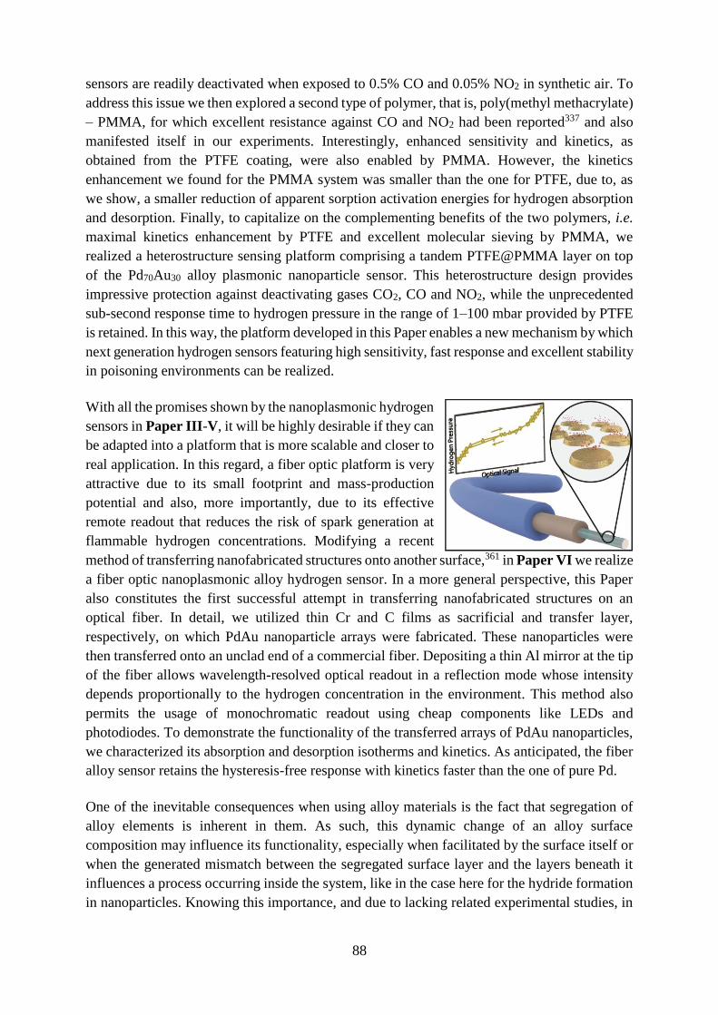
plasmonic response and the amount of hydrogen absorbed. In Paper III to V I demonstrate the
use of alloy nanoparticles as hydrogen sensors and report their relevant sensing metrics for
increasingly complex sensor configurations. Specifically, I use PdAu binary alloys in Paper
III, PdCu and PdAuCu ternary alloys in Paper IV and finally in Paper V, I combine the PdAu
alloy with different polymeric coating layers that serve as a molecular sieve to prevent sensor
deactivation, as well as, as it turned out, significantly increase sensor response time. Finally, as
an effort to further push the sensing platform closer to real applications, in Paper VI I try the
idea of integrating the alloy nanoparticles on an optical fiber by pattern-transfer of
lithographically made nanostructures from a flat host surface onto the fiber.
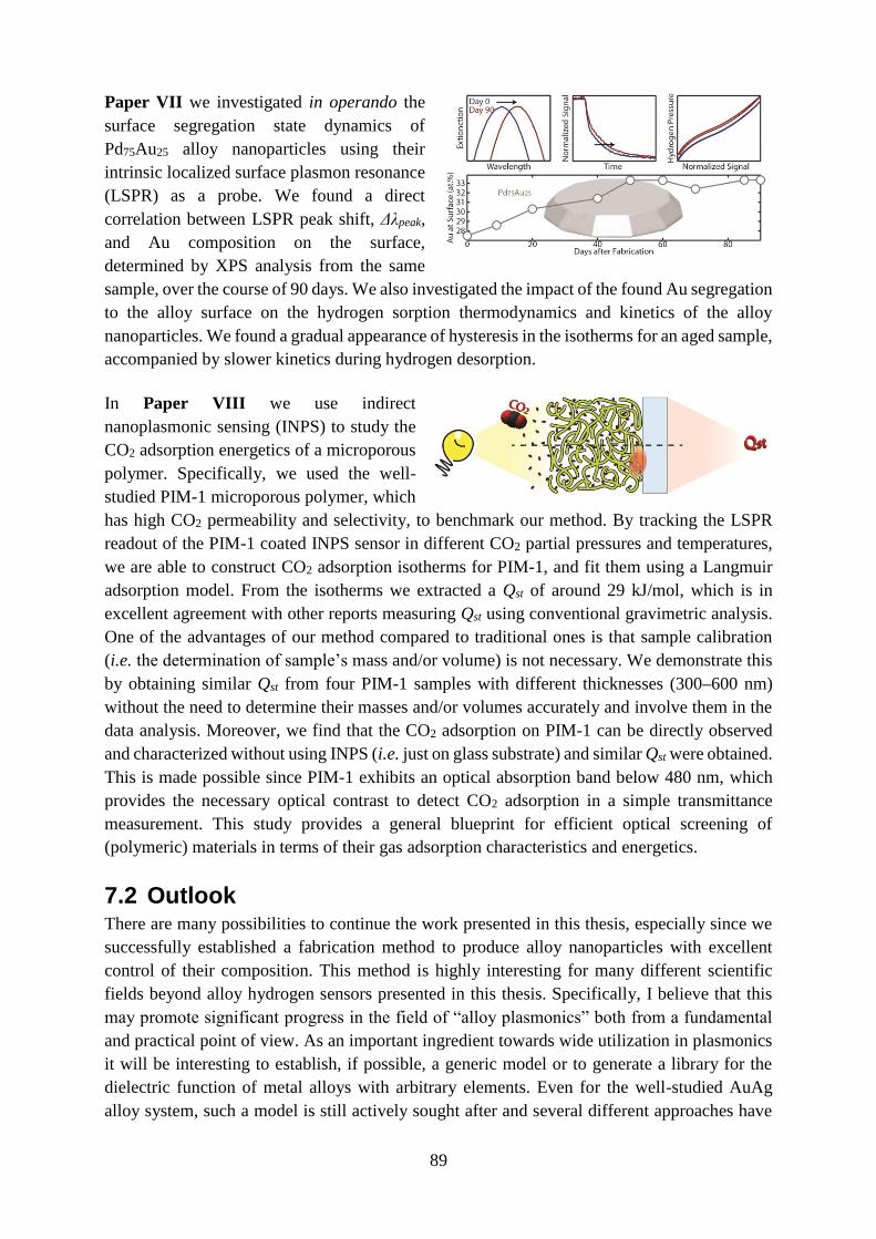
An almost inevitable consequence of working with alloys is the atomic segregation that may
occur from the bulk to the alloy surface. Owing to high sensitivity of nanoplasmonic sensors,
this process can actually be followed directly on the alloy nanoparticles I have developed, as
demonstrated in Paper VII using PdAu alloy as the model system.
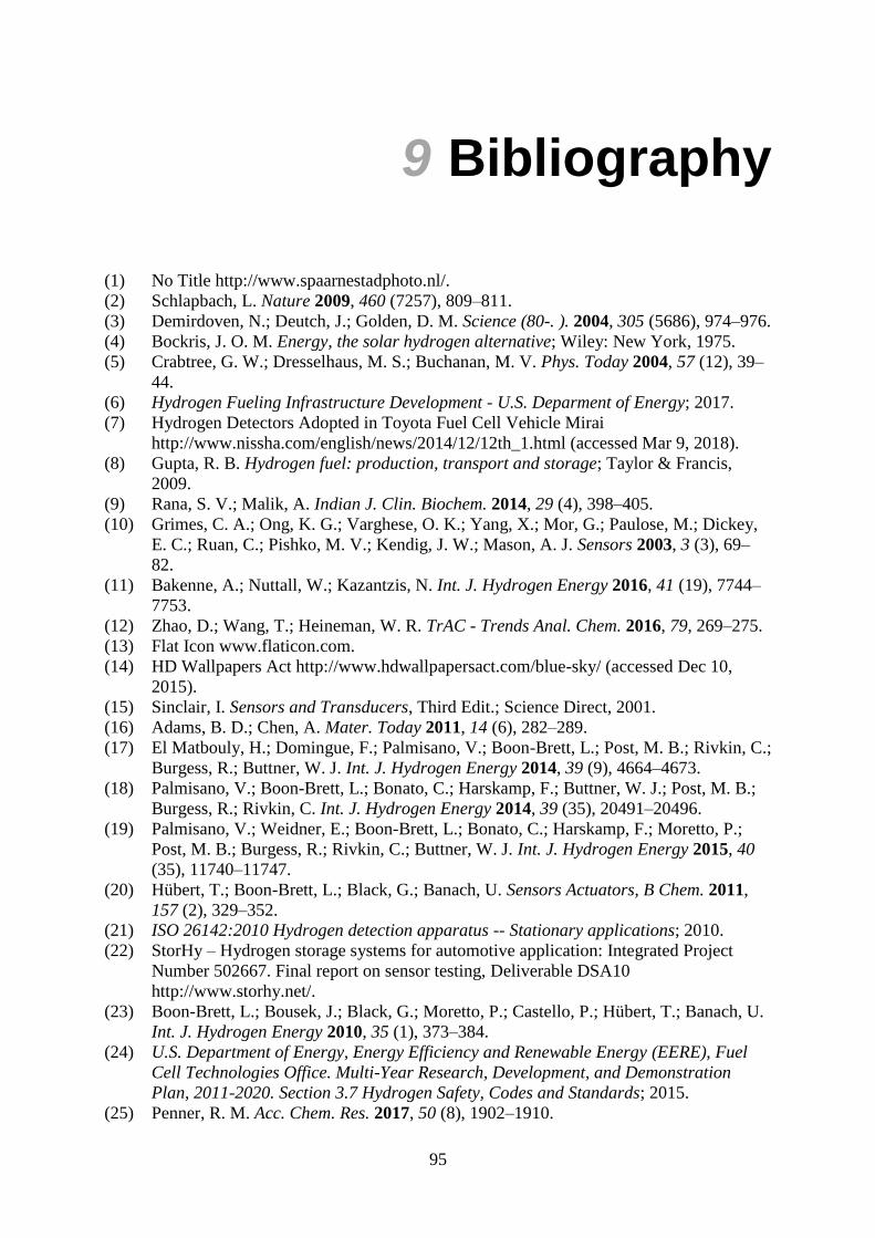
As a minor part of the thesis, I have also applied indirect nanoplasmonic sensing (INPS) to
characterize the CO2 adsorption energetics in a microporous solid sorbent material in Paper
VIII. Specifically, we studied PIM-1,77,78 a material that belongs to the rising class of
microporous polymers that exhibit high CO2 permeability and selectivity, which make them
10
attractive for Carbon Capture and Storage (CCS) applications.79–81
The organization of the remainder of this thesis is as follows: Chapter 2 introduces the
background physics to the LSPR phenomenon, with particular focus on the mechanisms
through which metallic nanoparticles supporting LSPR can be utilized as sensors. Chapter 3
discusses the basics of nanoalloys, including the surface segregation and their common
production methods. Chapter 4 provides an overview of metal hydride systems with particular
focus on the phenomena relevant for the interpretation of the work presented in the thesis. It
also includes a discussion about using metal hydrides as signal transducers in hydrogen sensors,
with specific emphasis on nanoplasmonic sensors. Chapter 5 describes the nanofabrication
techniques that I have developed and employed to make my samples. Chapter 6 explains the
different characterization methods I have used to assess the fabricated structures and sensors.
Finally, Chapter 7 summarizes the main results obtained in the appended papers, and I also
present a short outlook.
11
2 Nanoplasmonics
he field of nanoplasmonics, which explores localized surface plasmon resonance
phenomena in noble metal nanoparticles, has been rapidly developing for about two
decades. In simplest terms, a plasmon resonance is a coherent collective oscillation of
the free electrons in a metal. In the particle analogy it can be understood as the quantum of the
plasma oscillation (thus the –on suffix in plasmon). I believe this summary may not be sufficient
for most of the readers and so this Chapter is written to briefly introduce the field of plasmonics
and the concept of the localized surface plasmonic resonance. Furthermore, a well-developed
application of localized plasmons, their use in sensors – the central topic of this thesis, will also
be addressed.
2.1 Electrons in a Metal In order to understand the optical properties of materials one should, at the beginning, refer to
an approach developed by Hendrik Lorentz82,83 to explain how electrons in a metal behave
under the influence of an external electric field. In his model, better known as the Lorentz
Model, the optical properties of a material is described in terms of the response of a classic
harmonic oscillator to an external driving force. Electrons of matter are considered to be a
collection of identical, independent, isotropic harmonic oscillators oscillating back and forth
around their equilibrium position, i.e. the positively charged cores of the atom in the lattice of
the solid. When an external electric field E(x,t) acts upon these oscillators they follow the
equation of motion
𝑚𝑒�� + 𝑚𝑒𝛤�� + 𝑘𝒙 = −𝑒𝑬(𝒙, 𝑡) (2.1)
where me is the mass of the electron, x is the displacement from equilibrium, Γ is the damping
constant, k is the spring constant of the harmonic oscillator and e is the electronic charge. If the
applied field is harmonic with frequency ω and the oscillation amplitude is small so that the
field is approximately spatially constant, equation 2.1 has a single solution describing the
induced dipole of a single oscillating electron as
𝒑 = −𝑒𝒙 =
𝑒2
𝑚𝑒
𝜔02−𝜔2−𝑖𝛤𝜔
𝑬 (2.2)
where ω0 is the resonance frequency of the oscillator defined as
𝜔0 = √𝑘
𝑚𝑒 (2.3)
T
12
Assuming a system consisting of a large number, N, of independent electrons, the polarization
P (dipole moment per unit volume) can be calculated by multiplying N with equation 2.2. By
using the constitutive relation82
𝑷 = 𝜀0(𝜀 − 1)𝑬 (2.4)
A complex dielectric function ε(ω) for a system with a large numbers of independent electrons
can then be defined as
𝜀(𝜔) = 1 +𝜔𝑃
2
𝜔02−𝜔2−𝑖𝛤𝜔
= (1 +𝜔𝑃
2(𝜔02−𝜔2)
(𝜔02−𝜔2)2+𝛤2𝜔2) + 𝑖
𝜔𝑃2𝛤𝜔
(𝜔02−𝜔2)2+𝛤2𝜔2 (2.5)
The resonance frequency, ω0, originates from the restoring force experienced by an electron
bound to an atom while the damping constant, Γ, quantifies the associate inelastic processes,
and lastly the plasma frequency, ωP, is
𝜔𝑃 = √𝑁𝑒2
𝑚𝑒𝜀0 (2.6)
For an electric field with frequency ω < ωp the electrons will follow it and the dielectric function
ε is complex (i.e. has a real and imaginary part, see equation 2.5). Within the metal, the field
decays exponentially with the distance from the metal-dielectric interface. Therefore, the
incident field is attenuated and the electromagnetic field is reflected back from the surface. If
the opposite situation of ω > ωp occurs, the electrons inside the metal cannot respond fast
enough to screen the electric field. The refractive index ε is then real and the metal behaves as
a dielectric material i.e. the optical field is partly refracted and partly reflected. The bulk plasma
frequencies of metals are located in the ultraviolet spectral range, and thus the condition of ω <
ωp is fulfilled at the visible frequencies. This explains why metal surfaces appear shiny and
reflective to the human eye.
2.2 Localized Surface Plasmon Resonance When a metal entity becomes smaller and comparable to the wavelength of near-visible light,
its optical properties change dramatically. Under this circumstance the free electrons of the
particle can oscillate collectively when excited by the external optical electromagnetic field with
appropriate frequency. The oscillation typically decays within few femtoseconds due to the
significant damping (imaginary part of ε) characteristic for metals. The displaced electrons
(together with the rigid positively charged atomic cores) create a polarization field of their own,
which drives them back towards the equilibrium position. Due to the inertia, overshoot occurs
even in the absence of the external field. When the frequency of the applied field matches with
the system’s eigenfrequency, a collective coherent resonance occurs. The size of the
nanoparticle also imposes a boundary condition that prohibits the formation of a propagating
longitudinal charge density wave, i.e. like in the case of bulk and surface plasmon resonance.
Instead, in a simple picture, a standing electron wave oscillation with respect to the atomic core
is accomplished. Hence the name localized surface plasmon resonance (LSPR).
13
LSPR is one of the best examples of how things may change significantly at the nanoscale. At
the LSPR frequency, metal particles effectively scatter and absorb light, which gives rise to a
strong peak in their light extinction (i.e. sum of scattering and absorption) spectrum, which later
defines the “color” of the particles. Furthermore, the charge separation at the particle surface
gives rise to a strong electric field close to the surface. Figure 2.1 shows a schematic illustration
of the collective motion of the free electrons under the applied field. It corresponds to an
oscillating time-dependent electric dipole, which gives rise to an induced electric field due to
the charge separation. Two higher order modes of the LSPR, which may play a role for bigger
particles, are also shown.
Figure 2.1. Schematic illustration of localized surface plasmon resonance in a small metal
sphere. (a) The external electromagnetic field created by irradiated light drives the electrons
of the nanoparticle out of their equilibrium positions relative to the positively charged atomic
cores. The free electrons oscillate collectively with largest amplitude when the light frequency
matches their resonance or eigenfrequency. (b) Due to the oscillating charges, which lead to a
polarization of charge on the surface of the nanoparticle, a strong electric field is developed in
the vicinity of the particle. (c) For larger nanoparticles (relative to the wavelength), higher
modes of the LSPR exist, for example quadrupole and octupole modes.
LSPRs can typically be excited in the ultraviolet (UV), visible, and near infra-red (NIR) range
of the electromagnetic spectrum. The excitation represents a time-dependent dipole that
generates a strong local field, which is superimposed on the external field that drives the
oscillation. Thus, due to the resonant nature of the excitation, the local field around the
nanoparticles (near-field) is enhanced. This field can act as a probe of the nanoparticles’
surrounding and makes the LSPR very sensitive to changes of the permittivity of the medium
in the vicinity of the particle, as e.g. induced by molecular adsorption on the particle surface.
Higher refractive index of the surrounding means higher polarizability, which in turn increases
the screening of the dipolar field of the LSPR. The increased screening dampens the electron
oscillation and, thus, decreases its energy (spectrally red-shifts the resonance, i.e. moves it
towards longer wavelength). The plasmon energy is one key parameter in the characterization
14
of LSPR, and it is also commonly used as the main readout in sensing applications.31,45,84 A
detailed explanation of the sensing applications based on LSPR will be given in Section 2.3.
The lifetime of a typical LSPR excitation is in the range of 5-25 femtoseconds, depending on
particle size, shape and material. There are two ways in which LSPR can be damped: radiatively
and non-radiatively. The radiative damping process occurs when a photon of the same energy
as the incident one is re-emitted from the particle.85,86 Light that decays radiatively thus
corresponds to an elastic scattering process of electromagnetic energy by the induced dipole
and is referred to as scattering. The second damping process, non-radiative, involves dissipation
either via electron-hole pair excitation (from below to above the Fermi level, also called as
Landau damping) and, ultimately, production of heat through electron-phonon coupling.85,86
Light that decays non-radiatively is referred to as being absorbed by the nanoparticle.
Additionally, existence of adsorbates on the surface of the nanoparticle may also contribute to
plasmon damping. This effect is commonly referred as chemical interface damping.83
The sum of absorption and scattering is called optical extinction, which corresponds to the total
attenuation of the electromagnetic wave as it traverses a particle. The efficiency of the two
decay mechanisms can be expressed through their respective cross-sections (i.e. how efficient
the processes are). The analytical expressions for absorption, scattering, and extinction cross
sections of a nanoplasmonic particle much smaller than the wavelength are82
𝜎𝑎𝑏𝑠 = 𝑘Im(𝛼) (2.7)
𝜎𝑠𝑐𝑎 =𝑘4
6𝜋|𝛼|2 (2.8)
𝜎𝑒𝑥𝑡 = 𝜎𝑎𝑏𝑠 + 𝜎𝑠𝑐𝑎 (2.9)
where α is the material polarizability (see below) and k is the wave vector.
The extinction cross section offers a convenient way to describe the interaction between light
and nanoparticles. For a non-transparent object that does not resonantly interact with the
electromagnetic field, the extinction cross section is equal to the projected geometric area of
the particle and independent of the wavelength, i.e. only the light directly impinging on the
particle will not be transmitted. For the case of strongly interacting particles, the extinction
cross section depends on the wavelength and can be significantly larger than the projected
geometric area of the particle. This is the reason why plasmonic nanoparticles appear colored
(see e.g. Lycurgus Cup in Chapter 1). When white light hits the particles, a (major) part of the
wavelengths of the incident light is attenuated, leaving the rest of the wavelengths transmitted,
hence creating the “colored” appearance of the cup.
2.2.1 Understanding LSPR: The Electrostatic Approximation
A simple way to understand LSPR is the electrostatic approximation in the so-called quasi-
static regime. This model considers the particle diameter D to be small compared to the
wavelength of light (D << λ). This means that, in a first approximation, the electron oscillation
15
of the plasmon can be modeled as a point electric dipole. The mathematical form can be
constructed if one considers a homogeneous, isotropic nanosphere placed in an arbitrary
medium and subjected to a time-dependent external field E0e-iωt. The induced local field of the
particle then superimposes with the applied field, creating a dipole moment that can be
described as
𝑷(𝜔) = 𝜀𝑑𝛼(𝜔)𝑬𝟎𝑒−𝑖𝜔𝑡 (2.10)
where εd is the dielectric constant of the surrounding medium and α(ω) is the dipole
polarizability of the nanosphere. Gustav Mie, a German physicist, presented the exact solution
of the light-metal nanoparticle interaction by solving Maxwell’s equation more than a century
ago.37 According to his work, famously known as Mie Theory, the polarizability α(ω) of the
nanosphere reads as
𝛼(𝜔) = 4𝜋 (𝐷
2)
3 𝜀𝑚(𝜔)−𝜀𝑑
𝜀𝑚(𝜔)+2𝜀𝑑 (2.11)
where εm(ω) is the complex dielectric function of the nanosphere material. The magnetic
permeabilities are assumed to be as in vacuum for both the sphere and the external medium; a
reasonable assumption for optical frequencies.83 Equation 2.11 shows that the polarization
becomes very large when the denominator is equal to zero (at resonance), i.e. εm(ω) = -2εd. This
condition requires the dielectric constant of the particles to have a negative real part ε1(ω) and,
preferably, a small imaginary part ε2(ω) (i.e. small losses) for a strong polarization to occur.
Inserting the Drude dielectric function into the expression for the dipole polarizability (equation
2.11) yields
𝛼(𝜔) ≈ 4𝜋 (𝐷
2)
3 𝜔2𝐿𝑆𝑃𝑅
𝜔2𝐿𝑆𝑃𝑅−𝜔2−𝑖𝛤𝜔
(2.12)
where
𝜔𝐿𝑆𝑃𝑅 =𝜔𝑃
√1+2𝜀𝑑 (2.13)
or, if we use wavelength instead of frequency as we commonly do in measurements:
𝜆𝐿𝑆𝑃𝑅 = 𝜆𝑝√1 + 2𝜀𝑑 (2.14)
where λLSPR is the localized surface plasmon wavelength. The λLSPR is generally larger than the
wavelength of the bulk plasmon, λp. Equation 2.14 indicates that the spectral position of the
LSPR in the quasi-static limit depends purely on the surrounding dielectrics (i.e. 𝜀𝑑) and the
material itself (reflected through 𝜆𝑝). However this is not entirely true since for very small
particles (< 10 nm) the dielectric function of the metal is size-dependent. For larger particles,
size-dependent retardation effects also influence the LSPR spectral position.83 These effects
will be explained in the next section.
16
One can also insert the dipole polarizability (equation 2.11) into the expressions of scattering
and absorption cross sections (equation 2.7 and 2.8). This yields
𝜎𝑎𝑏𝑠 = 𝑘Im(𝛼) = 4𝜋𝑘 (𝐷
2)
3
Im (𝜀𝑚(𝜔)−𝜀𝑑
𝜀𝑚(𝜔)+2𝜀𝑑) (2.15)
𝜎𝑠𝑐𝑎 =𝑘4
6𝜋|𝛼|2 = 8𝜋 (
𝐷
2)
6
𝑘4 (𝜀𝑚(𝜔)−𝜀𝑑
𝜀𝑚(𝜔)+2𝜀𝑑)
2
(2.16)
Thus, the absorption is proportional to the sphere volume (D3) while scattering is proportional
to the square of the volume (D6). Thus, for very small particles, absorption dominates, while
scattering dominates LSPR decay for larger particles. For example in gold nanospheres and
nanodisks, this transition occurs for particle diameters around 80 nm and 100 nm,87,88
respectively. An example of an extinction spectrum (that is, the sum of absorption and
scattering) for an array of plasmonic nanodisks fabricated by hole-mask colloidal lithography
(explained in Chapter 5) is plotted in Figure 2.2.
Figure 2.2. Extinction spectrum of a gold nanoparticle array. A quasi-random array of gold
nanodisks with diameter of 190 nm and height of 25 nm, fabricated by hole-mask colloidal
lithography (HCL) on glass features a peak-like extinction spectrum. LSPR gives rise to a
strong extinction peak due to efficient scattering and absorption by the gold nanoparticles
around 650 nm. This particular extinction spectrum corresponds to a bluish color of the
nanoparticles.
2.2.2 LSPR Dependence on Particle Size, Shape and Composition
The discussion of the LSPR phenomenon in Section 2.2.1 was entirely based on the spherical
particle approximation in the quasi-static regime, which is sufficient to give a basic idea about
LSPR. However, in reality, various shapes and sizes of nanoparticles can be fabricated and are
used for real applications. Therefore, since the polarizability of differently shaped particles is
not the same as for a sphere, the scattering and absorption characteristics of such particles are
different. It is thus essential to have extended models and approaches to explain the plasmonic
17
properties of more complex nanostructures. By knowing the factors defining the LSPR, one can
freely “design” the resonance to be most suitable for a specific application. Below a short
discussion of the role of size/shape and material composition of the nanoparticle on the LSPR
is presented.
For a particle larger than the quasi-static approximation range (i.e. where D << λ no longer
applies), retardation effects and radiation damping become very important. Retardation of the
applied field arises when the particle size is comparable to the wavelength and the field
distribution is no longer homogeneous over the entire particle. A second retardation effect
affects the field inside the particle since it takes time for the dipolar field to spread over the
particle due to the finite speed of light. This retards the formation of the dipole and leads to a
phase shift between the dipolar plasmonic and the exciting field of the irradiated light wave.
These retardation effects induce a spectral red shift of the plasmon resonance, as well as peak
broadening.89
Radiation damping originates from the energy loss of the time-dependent dipole via emission
of radiation. This radiative plasmon decay channel thus becomes rapidly more significant for
bigger particles since the dipole is proportional to the size of the nanoparticles, and the
scattering cross section scales with D6 (see equation 2.8). Radiation damping also introduces a
spectral red-shift, an increase in plasmon line-width and a decrease in the resonance intensity.90
Larger nanoparticles also feature multipolar modes (see Figure 2.1c for the case of nanosphere
particles), which means that the resonance band splits into several peaks which appear at shorter
wavelength than the dipolar peak in the extinction spectrum.91
When addressing the material-dependence of LSPR, let us recall that a plasmon is an electron-
based phenomenon. Thus, its properties strongly depend on the electronic structure (as
described by the complex dielectric function) of the system within which it is excited.
Theoretically, LSPR excitations are possible in any material possessing large negative real part
and small imaginary part of the dielectric function. In fact, recent years have seen the emergence
of non-metal plasmonics e.g. dielectrics92 and semiconductors.93–95 Gold and silver are the
“classic” nanoplasmonic materials since they are the main systems chosen in LSPR studies due
to their low losses in the visible frequency range. Hence, they exhibit strong and reasonably
narrow LSPR peaks (Figure 2.2). Moreover, they feature LSPR in the visible range and their
properties can be reasonably well explained by the Drude model in the vis-NIR range, i.e. below
the interband transition threshold (2.4 eV for gold and 3.8 eV for silver, respectively96).
However, with increasing interest in LSPR and demands for applications in various fields, an
increasing number of materials have been studied for their plasmonic properties. Thus,
experimental reports on LSPR in, to name a few, Pt, Pd, Cu, Ni, Sn, Y, Mg and Al have become
available.97–105 Furthermore, alloys have also been considered for plasmonics, however only to
a very limited extent.106–109 For example, it has been shown for AuAg alloy nanoparticles that
their LSPRs can be tuned to anywhere between that for pure Au nanoparticles to that of Ag
nanoparticles by adjusting the alloy composition (also see Figure 2.3).110–112 LSPR
characteristics of some other alloy systems have also been demonstrated (e.g. AuCu108,113 and
AuFe107), however, only in a very limited fashion due to lack of versatile and reliable methods
18
for fabricating alloy nanoparticles. Lastly, a phase transformation of a material can also induce
significant changes to LSPR since the transition changes the electronic structure and/or volume
of the nanoparticles significantly. A prominent example, which also is relevant for this thesis,
is Pd when it is absorbing hydrogen (and thus phase-transforms to palladium hydride PdHx),
which leads to a considerable change in its electronic density of states due to weakened
interactions between Pd atoms induced by interstitial hydrogen.114,115
Figure 2.3. The LSPR dependence on material composition and particle dimensions. (a) The
different LSPRs exhibited by pure Ag, Pd, Cu and Au nanodisk arrays with dimensions of 190
nm diameter and 25 nm height. Note that the LSPR of Pd is much weaker and broader compared
to the rest. (b) The evolution of LSPR for AuAg alloy nanodisks with different compositions (Au
from 0–100 at. %, in 10 at. % steps). The dimensions are 190 nm diameter and 25 nm height.
(c) The change in LSPR in 50:50 AuAg alloy nanodisks with increasing diameter of 140 nm,
170 nm, 190 nm and 210 nm. The thicknesses are kept constant at 25 nm. (d) The change in
LSPR of Pd nanodisks with dimension of 190 nm diameter and 25 nm height when exposed to
hydrogen, resulting in palladium hydride, PdHx formation. Note that in panel (b) and (c)
extinction is normalized.
In addition to particle size and material, the optical properties of plasmonic nanoparticles are
also greatly influenced by their shape due to the polarizability’s, α(ω), shape dependency. Many
works have been devoted to study the shape-LSPR relation both experimentally and
theoretically. One of the fundamental works was done by Mock et al. in which they studied the
spectra of silver nanoparticles with different shapes (spheres, triangles, and cubes) but similar
19
volume.116 The study concluded that structures with shaper features have higher refractive index
sensitivity (i.e. sensitivity towards the change in surrounding permittivity). The result was also
supported by similar finding in other reports.117,118 In general, the deviation from spherical
shape shifts the resonance towards longer wavelength due to higher concentration of charge
and electric field at the sharp features.119,120 Apart from the general shape of the particles, aspect
ratio (i.e. ratio of width to height) also affects the resonance. High aspect ratio structures
(towards a one-dimensional structure) have longer resonance wavelength and higher LSPR
intensity.119,121 The reason for this is the high charge accumulation in such structures, which
leads to higher restoring force and consequently longer resonant wavelength. Figure 2.3
showcases the wide tunability of LSPRs achieved in this thesis by changing the plasmonic
elements’ composition (through change of materials, alloying and phase transition) and
dimension.
2.3 LSPR Sensors The LSPRs of nanoparticles are strongly dependent on many factors, as discussed in previous
sections, i.e. shape,116 size,122 material98 and the dielectric function of the surrounding
environment.123 Using the fact that the refractive index, n, of a material is related to its dielectric
function through 𝜀𝑑 = 𝑛2, equation 2.14 can be written as
𝜆𝐿𝑆𝑃𝑅 = 𝜆𝑝√1 + 2𝑛2 (2.17)
We see that the spectral position of the LSPR (λLSPR) depends approximately linearly on the
refractive index of the surrounding medium. This sensitivity, caused by the existence of the
enhanced field in the vicinity of the plasmonic nanoparticles, makes it possible for LSPR to be
used as a sensor; a nanoplasmonic sensor. The enhanced field can be considered to act as a
nanoscale probe of events taking place very closely to the plasmonic particle surface, within
the volume of enhanced field. This constitutes a highly localized sensing volume that allows
one to observe any change (e.g. adsorbate interaction, phase transition, etc.) occurring near the
particle surface if such a change results in a modification of the local refractive index.
Figure 2.4 schematically illustrates the sensing volume for the case of a nanodisk in vacuum.
Figure 2.4. A simplified illustration of the sensing volume around a plasmonic nanodisk in
vacuum. The sensing volume (red areas) is created by the enhanced electromagnetic field
surrounding a plasmonic entity. Within it, local permittivity changes are detected as a spectral
shift of the plasmonic peak.
The use of a nanoplasmonic sensor to detect changes in the surrounding was first done exactly
20 years ago by Englebienne,124 who employed Au nanoparticles to detect the occurrence of
20
antigen binding to ligands attached to the nanoparticles. By following the λLSPR, the binding
process could be followed in real time. Figure 2.5 illustrates how an LSPR sensor detects the
binding of analyte molecules onto the particle. The presence of analytes increases locally the
refractive index, which in turn alters the resonance condition of LSPR, causing it to red-shift.
Figure 2.5. Schematic illustration of an LSPR-based local refractive index sensor. Analyte
binding leads locally to higher refractive index in the vicinity of the nanoparticle. The increase
in the refractive index is detected as a red-shift of the nanoparticle LSPR. The figure is adapted
with modification from ref. 125.
Figure 2.6 shows the three typical “fingerprints” of LSPR that all can be used as readout
parameter in a nanoplasmonic sensing experiment, (i) a change in peak position, λpeak, (ii)
extinction at peak (Ext @ Peak), and (iii) full width at half maximum, FWHM. They all have
in common that they are the descriptor of a “physically meaningful” change of the LSPR effect.
As described above, λpeak is correlated with the resonance frequency. Furthermore, Ext @ Peak
corresponds to the extinction cross section and the FWHM is characteristic for the damping of
the LSPR. Most often, all three readouts change simultaneously. However, one cannot say in
general which one of these readouts gives the “best result” since they might be more sensitive
to different aspects of the sensed process and thus relate to different phenomena. Therefore, the
readout parameter should be chosen carefully in order to get as good and as physically relevant
signal as possible for the particular system studied. At the same time, the combination of
different readout parameters may also provide deeper insight into the studied process at hand,
compared to looking at one parameter alone.126
The simple yet powerful concept of nanoplasmonic sensing has made it a widely used analysis
technique across different fields. So far, biosensors is by far the most exploited application area
of nanoplasmonic sensing since it is label-free; thus it is very suitable for biological and
biomedical assays.45,127,128 Ever since the first demonstration by Englebienne,124 numerous
prototypes of LSPR refractive index sensors have been used to detect biological interactions
21
including, but not limited to, DNA-DNA,129 carbohydrate-protein,130,131 lipid-protein,132 and
protein-ligand binding.133–135 Over the years, a tremendous diversification of applications of
nanoplasmonic sensing has taken place. A prominent example is the growing application of
nanoplasmonic sensing in catalysis48,136 and chemical sensing.49 In the field of catalysis, after a
seminal work by Novo et al.,46 nanoplasmonic sensing has shed light on different catalytic
process such as photocatalysis,137,138 metal-hydrogen interactions,56,57 redox reactions139 and
spillover effects.140 For chemical sensing, especially for the gas phase, nanoplasmonic sensing
has been explored to detect, just to name a few, CO,141,142 CO250,51 and H2.
52,143,144
Figure 2.6. The “fingerprints” of LSPR. The LSPR extinction peak can be characterized by
three physically relevant parameters: λpeak (red arrow) denotes the wavelength where the peak
occurs and thus denotes the resonance frequency of the plasmon. Extinction @ Peak (green
arrow) shows the extinction value at λpeak and denotes the extinction cross section. Lastly, the
full width at half maximum (FWHM), depicted by the blue dashed line, characterizes the width
of the peak taken at half of the maximum extinction value and corresponds to the lifetime of the
plasmon in energy space. It is also common to define FWHM as twice the length of the fraction
of the line-width taken from the high energy (HE) and low energy (LE) side to the λpeak, as
marked by a and b respectively. Thus FWHMLE = 2b and FWHMHE = 2a. FWHMLE is mainly
used to avoid convolution with e.g. higher-order plasmonic modes.
The growing number of applications of nanoplasmonic sensors proves their versatility, which
indeed is one of their greatest strengths. One reason is that the strong dependence of the LSPR
frequency on size, shape and permittivity of the local surrounding offers practically viable
possibilities to actively tune the sensor response to a wavelength of choice by engineering these
parameters during the fabrication of the nanoparticles. This feature paired with ultra-high
sensitivity makes it possible that very small amounts of analyte (even single molecules45,145) or
even the tiniest changes in the sensor environment are enough to trigger the plasmonic signal.
That said, the quest for “ultimate sensitivity” is still ongoing and many different nanoparticle
designs have already been investigated.31,47 This ranges from the simpler shapes, like spheres56
and disks,146,147 to more complicated ones, like rings,33 cubes,148,149 stars150, rice53,54 etc.
22
Versatility is paired with additional advantages of nanoplasmonic sensing. For example, the
method provides in situ measurement compatibility even in harsh environments, real-time and
remote readout, and the possibility of massive miniaturization and parallelization. The
miniaturization can be forced down to single nanoparticles because even single plasmonic
nanoparticles can be used as signal transducers in sensing experiments.55,56,58,59,145,151,152 The
parallelization opportunities come as a consequence of the small size of the signal transducer
in nanoplasmonic sensors. A very large number of nanoparticles can be placed on the surface
of the sensor chip and each and every one of them can, in principle, be tailored to e.g.
specifically detect one type of molecule only. These extraordinary properties of nanoplasmonic
sensors are universal. Thus, one can take advantage of their abilities and apply them in many
different fields, as briefly discussed above.
As any technique, LSPR sensing also has its drawbacks and it is important to be aware of them.
One of the main limitations is a direct consequence of one of the main advantages: the high
sensitivity. In combination with the non-specificity of the readout (i.e. what is measured is a
“shift” of a peak), this may lead to data which are complicated to interpret since different
processes occurring simultaneously with/in the vicinity of the plasmonic particle all will give
rise to a signal. As a consequence, it is very important to design experiments properly so that,
ideally, conditions during measurement are such that the measured plasmonic signal originates
entirely from the event of interest. Failing to do so results in the convolution of different signals.
As one ingredient for minimizing this problem, gold (and silver, which, however, easily
oxidizes) is mainly used as plasmonic nanoparticle in sensing applications since it is, within
certain bounds, non-reactive. Thus the possibility of signal stemming from changes of the
plasmonic nanoparticles themselves, i.e. oxidation, reaction with adsorbate or alloying with
other metals, is minimized (though, when intended, this change of the nanoparticles themselves
can serve as powerful sensing method, as discussed in the next section). Such effects can
otherwise cause severe problems when measuring at elevated temperatures. Hence, in order to
use LSPR sensors in more dynamic (i.e. under reactive gases and/or elevated temperature)
environment, and thus broaden the applicability of LSPR sensors and make them more
universal, these limitations must be overcome. Interestingly, one simple alternative has been
developed in order to tackle some of those limitations and it will be discussed in a section
below.
2.3.1 Direct Nanoplasmonic Sensing
If we recall the discussion above, especially equation 2.17, it is clear that λLSPR of
nanoplasmonic particles depends on their actual state, and thus can be used to study changes in
their own intrinsic properties (i.e. shape, size, and material of the particles). Thus, any alteration
to the plasmonic particles themselves, either physically (e.g. shape and size) or chemically (i.e.
phase change like oxidation, melting, hydride formation, etc.), affects the LSPR spectra, which
means that such processes can be qualitatively (and quantitatively) observed by monitoring the
corresponding changes in the LSPR spectra (Figure 2.7). The approach where the LSPR of the
nanoparticle itself is used to monitor changes to the particle is usually called direct plasmonic
sensing and was coined by our group.48 In the past few years, this type of sensing has expanded
23
the applicability of plasmonic sensing to the field of materials science. Examples of such studies
include the hydride formation in palladium,52,56,57,59,153 magnesium,105 and yttrium
nanoparticles,100 oxidation of aluminum104 and copper nanoparticles,102,154 freezing/melting of
tin nanoparticles101 and dealloying of AuAg alloy nanoparticles.155
Even though direct nanoplasmonic sensing has facilitated many interesting insights and thus is
proven very useful, it is only limited to materials which themselves sustain LSPR. This greatly
limits the materials and particle sizes available for study. As one of the ways to circumvent this
problem, indirect nanoplasmonic sensing has been proposed.
Figure 2.7. Direct plasmonic sensing. Change in a plasmonic nanoparticle induces a
modification of the optical properties and thus can be followed by tracking the λpeak. The change
may include shape, phase (e.g. oxidation, hydride formation) and temperature.
2.3.2 Indirect Nanoplasmonic Sensing (INPS)
A specific type of LSPR sensing is called Indirect Nanoplasmonic Sensing (INPS).147 The key
feature of the method is the use of thin dielectric layers, which can be deposited by either
sputtering or chemical vapor deposition (CVD) methods (detailed explanation in Chapter 5).
In INPS, such layers are applied to cover an array of plasmonic (usually Au or Ag) nanoparticles
in order to separate the optically active sensor particles from the materials of interest, which are
simply deposited on top of the dielectric layer. Therefore, the active plasmonic nanoparticles
are physically separated from and do not interact with the materials deposited onto the dielectric
layer; thus the name indirect sensing. Despite the separation, the sensing functionality is still
accessible since the enhanced LSPR field penetrates through the dielectric layer, which
typically is only a few to ten nanometers thin. Figure 2.8 shows a schematic depiction of the
architecture of the INPS platform and its sensing principle.
This simple addition of a dielectric layer provides an efficient solution to some of the LSPR
sensor shortcomings described above. For example, it is able to contain the shape of the gold
nanodisks even at high temperatures, and prevents contamination, alloying, or reaction of the
gold nanodisks with the materials being deposited on the sensor. Furthermore, the spacer layer
can provide a tailored and homogeneous surface chemistry of the INPS sensor chip for a specific
24
experiment, where it either can constitute an inert substrate for the nano- or thin film materials
to be studied or participate actively in the process under study (Figure 2.8).
Figure 2.8. Nanoarchitecture and sensing principle of indirect nanoplasmonic sensing. A
thin dielectric layer is deposited on the plasmonic (e.g. Au or Ag) nanoparticle sensors to
physically separate them from the nanomaterials to be studied. The latter can be small
nanoparticles or thin films (solid or porous) and are simply deposited on top of the dielectric
layer. Any change to the studied materials located within the sensing volume of the plasmonic
nanoparticles (e.g. phase transition, adsorption of molecules/materials, rearrangement, etc.) is
detected as change in the LSPR fingerprint parameters.
Since its invention nearly a decade ago, INPS has contributed to several important
developments towards opening up the applicability of nanoplasmonic sensing to other than
biosensing-related areas. In the original paper, three different applications were demonstrated
to show the versatility of the platform: the glass transition temperature of confined non-
conjugated polymers, the kinetics and thermodynamics of hydrogen storage in small Pd
particles (< 5 nm), and optical nanocalorimetry of hydrogen oxidation on a Pt nanocatalyst.147
Further exploitation of INPS resulted in more focused applications in heterogeneous catalysis
and materials science48,156–160 and renowned interest in biosensing,127,128,161–164 due to its
versatility and stability.
Nowadays, the definition of INPS is no longer limited to plasmonic sensor particles being
separated by a spacer layer. A configuration where the two entities are spatially separated (i.e.
located near each other, given that the distance is close enough so that the enhanced field of the
antenna reaches the probed materials) fulfills the definition of INPS.55,165–168 This is best
demonstrated by the work of Syrenova et al.56 where a single Au nanosphere (100 nm diameter)
is placed next to a Pd nanocube (< 60 nm side length). At this size, the Pd nanocube exhibits
very weak scattering and thus cannot be tracked optically. When the Pd transitions to PdHx, the
optical signal originates from Au change and thus the hydrogenation process can be followed.
25
3 Nanoalloys
ore than 4000 years ago, an important discovery was made by our ancestors by
smelting tin and copper together to produce bronze, a “new” metal that was harder
and more durable than other metals available at the time. This important discovery,
celebrated by assigning it to the period where it happened, the Bronze Age, provided significant
advantages that eventually led to better technology and society. The concept of combining two
or more different metals to produce a new system, the so-called alloy, that possesses better
properties, persists to this day. In this Chapter, I will briefly discuss the basics of alloys and
describe in more detail the palladium-noble metal alloy system due to its direct relevance for
my thesis work. Following that, a discussion about segregation occurring in alloys and how
alloy nanoparticles can be produced will be given.
3.1 Alloy Formation and Phase Diagram Alloys constitute an interesting class of materials due to their unique features exemplified
above: the synergistic combination of physical and chemical properties of their constituents or
even new functionalities. To be in line with the theme of this thesis, the superior properties of
alloys are best demonstrated on the example of AuAg alloy nanoparticles. As we have learnt
from the last Chapter, at the nanoscale, neat Au and Ag exhibit localized surface plasmon
resonance and both systems are considered to be the main plasmonic metals thanks to their
excellent optical properties. Individually, however, these two metals have their own
(dis)advantages relative to each other. Ag is considered to be the better plasmonic metal due to
lower optical losses, which results in a narrower LSPR peak. However, Ag is known to oxidize,
hampering its use in many applications. These characteristics are perfectly complemented by
Au, which is highly inert but features slightly worse LSPR properties. When combined together,
AuAg alloys may exhibit the inertness of Au while retaining the remarkable optical properties
of Ag. The case of the AuAg alloy is just an example. A large number of alloy systems have
been exploited to produce diversified hybrid materials that enable innovative applications
across fields.107,169–173
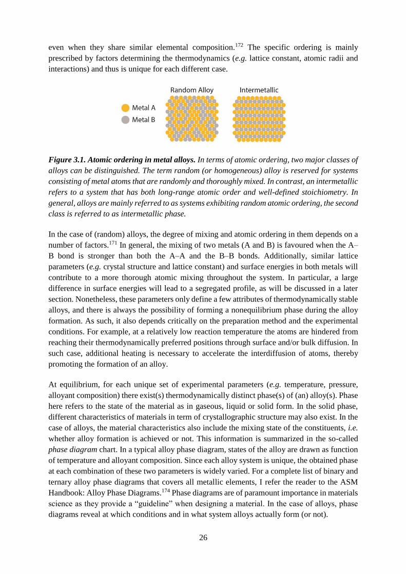
When mixing two elements together (from this point onwards I will limit the discussion only
to two-component, or binary, alloys), the atomic ordering in the system can take form into two
configurations: alloys and intermetallic compounds (Figure 3.1). In alloys, the two different
types of atoms are randomly and thoroughly mixed. In contrast, in an intermetallic compound,
the atoms are arranged orderly with well-defined stoichiometry. Although both types feature a
complete mix of the constituent atoms (and therefore are eligible to be called alloy), the term
of “alloy” is only used when one refers to the system with random distribution. This
classification is important as both types of systems can have significantly different properties,
M
26
even when they share similar elemental composition.172 The specific ordering is mainly
prescribed by factors determining the thermodynamics (e.g. lattice constant, atomic radii and
interactions) and thus is unique for each different case.
Figure 3.1. Atomic ordering in metal alloys. In terms of atomic ordering, two major classes of
alloys can be distinguished. The term random (or homogeneous) alloy is reserved for systems
consisting of metal atoms that are randomly and thoroughly mixed. In contrast, an intermetallic
refers to a system that has both long-range atomic order and well-defined stoichiometry. In
general, alloys are mainly referred to as systems exhibiting random atomic ordering, the second
class is referred to as intermetallic phase.
In the case of (random) alloys, the degree of mixing and atomic ordering in them depends on a
number of factors.171 In general, the mixing of two metals (A and B) is favoured when the A–
B bond is stronger than both the A–A and the B–B bonds. Additionally, similar lattice
parameters (e.g. crystal structure and lattice constant) and surface energies in both metals will
contribute to a more thorough atomic mixing throughout the system. In particular, a large
difference in surface energies will lead to a segregated profile, as will be discussed in a later
section. Nonetheless, these parameters only define a few attributes of thermodynamically stable
alloys, and there is always the possibility of forming a nonequilibrium phase during the alloy
formation. As such, it also depends critically on the preparation method and the experimental
conditions. For example, at a relatively low reaction temperature the atoms are hindered from
reaching their thermodynamically preferred positions through surface and/or bulk diffusion. In
such case, additional heating is necessary to accelerate the interdiffusion of atoms, thereby
promoting the formation of an alloy.
At equilibrium, for each unique set of experimental parameters (e.g. temperature, pressure,
alloyant composition) there exist(s) thermodynamically distinct phase(s) of (an) alloy(s). Phase
here refers to the state of the material as in gaseous, liquid or solid form. In the solid phase,
different characteristics of materials in term of crystallographic structure may also exist. In the
case of alloys, the material characteristics also include the mixing state of the constituents, i.e.
whether alloy formation is achieved or not. This information is summarized in the so-called
phase diagram chart. In a typical alloy phase diagram, states of the alloy are drawn as function
of temperature and alloyant composition. Since each alloy system is unique, the obtained phase
at each combination of these two parameters is widely varied. For a complete list of binary and
ternary alloy phase diagrams that covers all metallic elements, I refer the reader to the ASM
Handbook: Alloy Phase Diagrams.174 Phase diagrams are of paramount importance in materials
science as they provide a “guideline” when designing a material. In the case of alloys, phase
diagrams reveal at which conditions and in what system alloys actually form (or not).
27
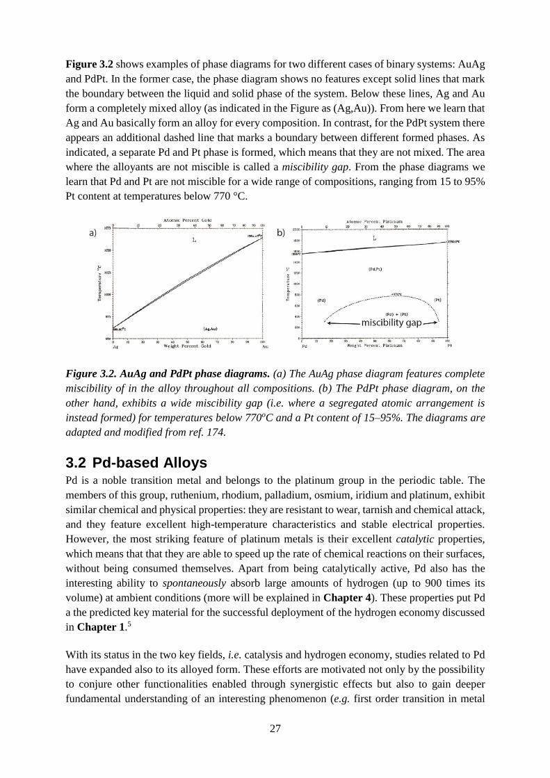
Figure 3.2 shows examples of phase diagrams for two different cases of binary systems: AuAg
and PdPt. In the former case, the phase diagram shows no features except solid lines that mark
the boundary between the liquid and solid phase of the system. Below these lines, Ag and Au
form a completely mixed alloy (as indicated in the Figure as (Ag,Au)). From here we learn that
Ag and Au basically form an alloy for every composition. In contrast, for the PdPt system there
appears an additional dashed line that marks a boundary between different formed phases. As
indicated, a separate Pd and Pt phase is formed, which means that they are not mixed. The area
where the alloyants are not miscible is called a miscibility gap. From the phase diagrams we
learn that Pd and Pt are not miscible for a wide range of compositions, ranging from 15 to 95%
Pt content at temperatures below 770 °C.
Figure 3.2. AuAg and PdPt phase diagrams. (a) The AuAg phase diagram features complete
miscibility of in the alloy throughout all compositions. (b) The PdPt phase diagram, on the
other hand, exhibits a wide miscibility gap (i.e. where a segregated atomic arrangement is
instead formed) for temperatures below 770oC and a Pt content of 15–95%. The diagrams are
adapted and modified from ref. 174.
3.2 Pd-based Alloys Pd is a noble transition metal and belongs to the platinum group in the periodic table. The
members of this group, ruthenium, rhodium, palladium, osmium, iridium and platinum, exhibit
similar chemical and physical properties: they are resistant to wear, tarnish and chemical attack,
and they feature excellent high-temperature characteristics and stable electrical properties.
However, the most striking feature of platinum metals is their excellent catalytic properties,
which means that that they are able to speed up the rate of chemical reactions on their surfaces,
without being consumed themselves. Apart from being catalytically active, Pd also has the
interesting ability to spontaneously absorb large amounts of hydrogen (up to 900 times its
volume) at ambient conditions (more will be explained in Chapter 4). These properties put Pd
a the predicted key material for the successful deployment of the hydrogen economy discussed
in Chapter 1.5
With its status in the two key fields, i.e. catalysis and hydrogen economy, studies related to Pd
have expanded also to its alloyed form. These efforts are motivated not only by the possibility
to conjure other functionalities enabled through synergistic effects but also to gain deeper
fundamental understanding of an interesting phenomenon (e.g. first order transition in metal
28
hydride formation) by deliberately changing the system parameters (e.g. lattice constant,
surface strain) through alloying. The large amount of literature reports related to Pd alloys is
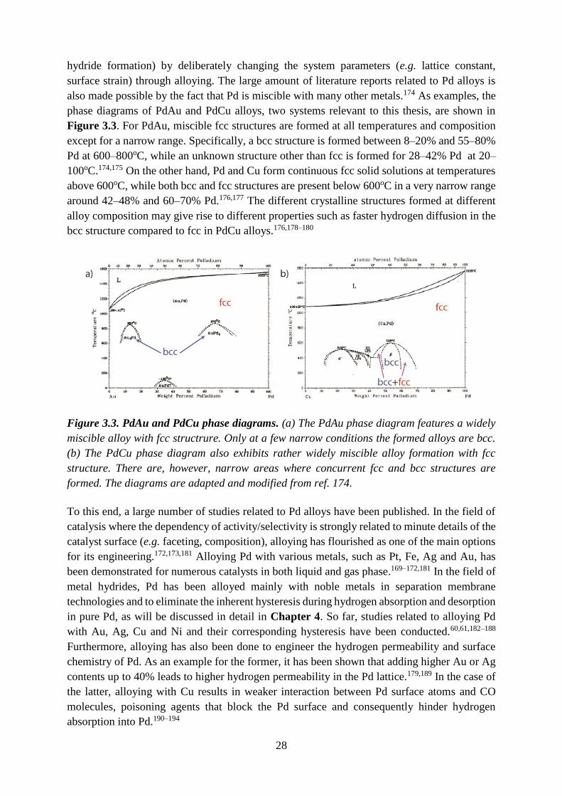
also made possible by the fact that Pd is miscible with many other metals.174 As examples, the
phase diagrams of PdAu and PdCu alloys, two systems relevant to this thesis, are shown in
Figure 3.3. For PdAu, miscible fcc structures are formed at all temperatures and composition
except for a narrow range. Specifically, a bcc structure is formed between 8–20% and 55–80%
Pd at 600–800oC, while an unknown structure other than fcc is formed for 28–42% Pd at 20–
100oC.174,175 On the other hand, Pd and Cu form continuous fcc solid solutions at temperatures
above 600oC, while both bcc and fcc structures are present below 600oC in a very narrow range
around 42–48% and 60–70% Pd.176,177 The different crystalline structures formed at different
alloy composition may give rise to different properties such as faster hydrogen diffusion in the
bcc structure compared to fcc in PdCu alloys.176,178–180
Figure 3.3. PdAu and PdCu phase diagrams. (a) The PdAu phase diagram features a widely
miscible alloy with fcc structrure. Only at a few narrow conditions the formed alloys are bcc.
(b) The PdCu phase diagram also exhibits rather widely miscible alloy formation with fcc
structure. There are, however, narrow areas where concurrent fcc and bcc structures are
formed. The diagrams are adapted and modified from ref. 174.
To this end, a large number of studies related to Pd alloys have been published. In the field of
catalysis where the dependency of activity/selectivity is strongly related to minute details of the
catalyst surface (e.g. faceting, composition), alloying has flourished as one of the main options
for its engineering.172,173,181 Alloying Pd with various metals, such as Pt, Fe, Ag and Au, has
been demonstrated for numerous catalysts in both liquid and gas phase.169–172,181 In the field of
metal hydrides, Pd has been alloyed mainly with noble metals in separation membrane
technologies and to eliminate the inherent hysteresis during hydrogen absorption and desorption
in pure Pd, as will be discussed in detail in Chapter 4. So far, studies related to alloying Pd
with Au, Ag, Cu and Ni and their corresponding hysteresis have been conducted.60,61,182–188
Furthermore, alloying has also been done to engineer the hydrogen permeability and surface
chemistry of Pd. As an example for the former, it has been shown that adding higher Au or Ag
contents up to 40% leads to higher hydrogen permeability in the Pd lattice.179,189 In the case of
the latter, alloying with Cu results in weaker interaction between Pd surface atoms and CO
molecules, poisoning agents that block the Pd surface and consequently hinder hydrogen
absorption into Pd.190–194
29
3.3 Surface Segregation in Metallic Alloys Thermodynamically, segregation of one or more constituents to the surface may occur for all
alloy systems regardless of temperature.195 The tendency of the segregated element (often also
identified as impurity) to diffuse to or from a surface may be expressed by its segregation
energy, that is the difference between total free energy between a surface site and bulk site.196
This means that positive segregation energy implies a tendency for an impurity to move into
the bulk, while negative segregation energy drives it to the surface. Expectedly, the segregation
energy for an element is different for different alloy systems, as well as for the environment
they are exposed to (e.g. in vacuum or in oxidizing atmosphere). The extent of the segregation
also depends on the type of facet of the surface and the size of the system (in the case of
nanoparticles), in which segregation features are more apparent with decreasing dimensions.197–
199 Nonetheless, the kinetics of the segregation process are strongly influenced by temperature,
that is, it occurs faster at higher temperature. At the end, enrichment of one or more constituents
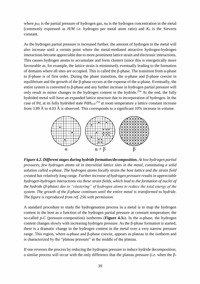
at the surface, and up to a few monolayers underneath, is obtained (Figure 3.4).
Figure 3.4. Surface segregation. Over time, one or more elements of an alloy can diffuse and
segregate to the surface, creating a different composition at the surface with respect to the bulk.
The segregating element depends on the alloy system and the environment it is exposed to. The
segregation process is kinetically driven by temperature.
Segregation creates a different composition at the alloy surface as compared to the bulk and
therefore the surface-related properties are expected to be altered. Hence, the functionality of
alloy particles enabled by their surface may be enhanced or weakened, depending on the
segregated elements. For example, Park et al. observed higher CO oxidation catalytic activity
of Rh50Pt50 nanoparticles over time and assigned surface segregation of Rh to be the primary
cause.199 On the other hand, Cui et al. used Pt40Ni60, Pt50Ni50 and Pt60Ni60 nanoparticles and
studied their oxygen reduction reaction (ORR) activity. They found for all alloys that the
activity drops up to 66% when Pt segregates to, and completely dominates, the surface.200
As discussed above, Pd-based alloys are one of the most studied systems due to their excellent
catalytic properties. Consequently, segregation phenomena in Pd-based alloys are also widely
scrutinized both experimentally and theoretically.201–203 Very recently, Zhao et al. generated an
analytical model to predict the surface segregation of 40 binary Pd alloys in vacuum at 600K,
whose results are in excellent agreement with the ones available in the literature.204 Some of
the interesting alloys are presented in Table 3.1. In the table, different Pd-based alloys are
shown together with the segregating element and also their equilibrium composition on the
surface with 25 at.% initial composition. Clearly, not only the segregating element varies for
different alloys, but also their equilibrium composition on the surface. For PdAu and PdCu
alloys, the two alloys of particular interest in this thesis, it is interesting to note that their extent
30
of segregation is totally different. For PdAu, strong Au segregation to the surface is expected.
On the other hand, PdCu has no tendency to segregate as the equilibrium Cu composition at the
surface barely changes to 26 at.%, an increase of only 1 at.% from the initial condition. These
calculations are in excellent agreement with experimental and theoretical studies and show that
indeed Cu and Au atoms segregate to the surface of the corresponding alloys.195,196,201,203,205
However, the extent of segregation is not as severe for Cu as Au due to its low segregation
energy.196,202
Table 3.1 Surface segregation for (111) plane of Pd alloys in vacuum at 600K.204
Alloy Segregation
Element
𝑥𝐴𝑠𝑢𝑟𝑓
of
Pd75A25 Alloy
Segregation
Element
𝑥𝐴𝑠𝑢𝑟𝑓
of
Pd75A25
PdAg Ag 52 PdMg Pd 17
PdAl Al 37 PdMn Mn 29
PdAu Au 71 PdNi Pd 3
PdCo Pd 2 PdPt Pd 1
PdCu Cu 26 PdY Pd 0
PdFe Pd 4 PdZr Pd 2
Knowing that segregation is an inevitable phenomenon in most of the alloy nanoparticles, and
how in many cases it deteriorates their intended functionality, it is thus of great importance to
be able to characterize the surface state of alloy nanoparticles. In order to do so, surface-
sensitive characterization techniques have been employed. Commonly used techniques include
high-resolution electron microscopy, atom probe tomography (APM) and x-ray photoelectron
spectroscopy (XPS). Without going into details, electron microscopy and APM are considered
to be invasive, in that they actually can interfere and alter the investigated sample due to i.e.
bombardment with high energy electrons or, in the case of APM, actual removal of materials.
Thus, these two techniques are compatible with the characterization of a sample at end of its
use, in its final state. In contrast, XPS is non-invasive but quite slow and time-consuming, as
will be explained in detail in Chapter 6. Finding a novel way to characterize segregation in
nanoparticles in situ and in real time to reveals its dynamics is thus highly desirable. Relying
on the fact that nanoplasmonic particles are surface sensitive (see Chapter 2), in Paper VII, I
demonstrated using PdAu as model system that the segregation occurring on alloy nanoparticles
can actually be tracked by monitoring the LSPR spectra, in particular through the change in
peak position λpeak. I found that the change in λpeak is proportional to the change of the PdAu
composition on the surface measured by XPS, and that the correlation between the two is in
good agreement with the literature.
31
3.4 Synthesis and Fabrication of Alloy Nanoparticles The widely interesting and tunable properties of alloy nanoparticles has created a need to
establish robust, reproducible and high-yield alloy nanoparticle production methods. Two main
methods can be categorized: wet-chemical synthesis and physical deposition methods.
3.4.1 Wet-Chemical Synthesis
Wet-chemical or colloidal synthesis refers to growth of solid metal nanoparticles via chemical
reaction in a liquid reaction medium. Wet-chemical synthesis is also called bench chemistry
since it is most often performed in lab benches and requires simple setups. This simplicity
(however please mind that simplicity of the equipment used here does not necessarily correlate
to the simplicity in obtaining the intended products) is also accompanied by other advantages,
such as high-yield, scalability and low-cost. Therefore, wet synthesis has been the main
technique to produce alloy nanoparticles. There are three distinct methods to produce alloy
nanoparticles, that is, co-reduction, thermal decomposition and seed-mediated growth.
3.4.1.1 Co-reduction
Co-reduction is possibly the most straightforward and simplest technique to produce alloy
nanoparticles, as it is commonly used as the main technique to synthesize monometallic
nanoparticles with different size and shape.172,206,207 The technique is based on the reduction of
metal salts (compounds in which the hydrogen of an acid is replaced by a metal e.g. AuCl3) by
reducing agents, which later transforms the metallic ions into neutral atoms (e.g. Mn+ M0, n
> 0). The free metallic atoms quickly nucleate into small metallic clusters, which become the
basis for the remaining formed neutral atoms to bind and consequently grow isotropically in
size. To synthesize alloy nanoparticles with different composition, simultaneously reducing
metal salt precursors with different molar concentration is done. Co-reduction has been largely
used to produce AuAg alloy nanoparticles.107,110,112,172,208–212
In many cases, one is interested in synthesizing nanoparticles not only with controlled
composition, but also shape and crystal orientation to achieve certain properties. In wet
synthesis, this can be achieved by employing surface capping agents that selectively bind to
specific facets of the nanoparticles, which subsequently block the growth in in corresponding
facets. To this end, different types of surface capping agents have employed, such as organic
ligands, polymers and surfactants, to produce alloy nanoparticles with different shapes, for
example cubes,213–215 tetrahedra214,215 and octrahedra.213,215 However, bound capping agents on
nanoparticles may significantly affect their surface properties. For example, in the application
of catalysis, capping agents may hinder the catalytic activity by blocking the active surface. It
is then important to establish proper cleaning procedures to remove the capping agents while
retaining the nanoparticle properties (e.g. shape, size and composition).
Despite its simplicity, co-reduction of alloys may not work for arbitrary metal components, as
the reduction rate, determined by a parameter called reduction potential, of each metal varies.
In short, the bigger the difference between the reduction potential of the metal components, the
less likely that the alloy produced has the intended composition, or is formed at all, as one
component reduces faster than the other. For example, in a mixture consisting of Au and Cu
32
(reduction potentials of 1.50 and 0.34 V, respectively), the Au will reduce faster than Cu,
resulting in alloys with higher Au content than expected. A way to synchronize the reduction
rate of the precursors is by varying their molar concentration.216 This, however, introduces
another complication as the determination of the needed precursor concentration for a certain
composition is different for different alloys, reaction temperature, used metal salts and solvents,
etc.
3.4.1.2 Thermal Decomposition
In thermal decomposition, reduction of metal precursors is not done by reducing agents but
rather, as the name suggests, by high temperature. Thus, thermal decomposition is mainly used
to synthesize monometallic or alloy nanoparticles comprising metals with low reduction
potentials (e.g. Fe, Co and Ni). Additionally, organometallic precursors (e.g. acetylacetonates
M(acac)n and carbonyls Mx(CO)y), which are readily decomposed under moderate heating, i.e.
150oC, are used instead.217,218 Thermal decomposition shares similar traits to co-reduction as
explained above. In fact, the two methods can be combined, as demonstrated by Sun and co-
workers who synthesized FePt nanoparticles by reducing the Pt and decomposing the Fe
simultaneously.219–221 A clear advantage of thermal decomposition compared to co-reduction is
the possibility to employ bimetallic precursors. This is made possible especially for carbonyl
precursors, by reacting one precursor with another.222 Thus, during synthesis, both metallic
atoms decompose simultaneously to form alloy nanoparticles. This drastically simplifies the
reaction mechanism (otherwise careful determination of precursors concentration has to be
done in order to match the reduction rates of the alloyants, as explained above) and provides
more precise control over the alloy composition, which is defined by the composition of the
bimetallic precursors. To this end, alloy nanoparticles comprising FeCO3, FePt, FeNi4 and Fe4Pt
have been successfully synthesized using bimetallic precursors.222,223
At this point it is important to discuss one key characteristic of nanoparticles produced by co-
reduction and thermal decomposition, that is, their polydispersity. Polydispersity refers to
variation in terms of size and shape of the nanoparticles, which might be undesired. In general,
during reduction of metallic atoms, they may undergo homogeneous or heterogeneous
nucleation. The former occurs when the concentration of atoms reaches a high enough level
(also called supersaturation), which leads to clustering and formation of stable seeds. The latter
takes place when the atoms are added directly to the surface of preformed seeds. The driving
force of heterogeneous nucleation is far less than homogeneous nucleation and thus can already
take place in the absence of homogeneous nucleation (i.e. self-nucleation), provided that the
atom concentration is kept below supersaturation, but high enough to overcome the
heterogeneous nucleation barrier. When both types of nucleation occur simultaneously, the
formed nanoparticles will be generally characterized by polydispersity, in shape and size, whose
degree increases as the reaction time extends. This is made worse by the sensitivity of
homogeneous nucleation to slight variation in e.g. temperatures. For this reason, both
coreduction and thermal decomposition have been so far used to synthesize nanoparticles with
size less than 30 nm.110,112,209,210,224–228 Beyond that, large variation in size and shape are
unavoidable, which makes utilization of produced nanoparticles in e.g. plasmonics, the main
theme in this thesis, very limited.
33
3.4.1.3 Seed-Mediated Growth
To circumvent the size limitation (as direct consequence of polydispersity) above, a more recent
technique called seed-mediated growth was developed. The concept behind this method is to
have seeds already existing in the solution, onto which atoms deposit, and thus prevent self-
nucleation.229–231 Precise control of the seeds, in particular their internal defect structure and
crystallinity, can facilitate growth of monodispersed nanoparticles with defined shapes with
relatively large dimensions.232,233
Despite this advantage, successful efforts on synthesizing alloy nanoparticles with dimension
beyond 50 nm are lacking. Only recently Rioux and Meunier demonstrated controlled synthesis
of AuAg alloy nanoparticles with dimensions ranging from 30 to 150 nm.234 They achieved this
by using multistep seeded growth. At the beginning they started with a small Au seed, which
later Au and Ag are grown onto. After a specific time they stopped the synthesis and used the
produced alloys as seeds for the subsequent step. By doing these steps repeatedly, excellent
control of the nanoparticle size with narrow distribution can be obtained. However, the resulting
alloys do not feature homogeneous composition over the nanoparticle. Instead, a gradual profile
was achieved, in which the Ag (Au) concentration increases (decreases) towards the surface.
All three wet synthesis methods described above has been the key workhorses for the vast
advancement in the field of colloidal particles and their applications. However, until today, we
rarely see their application in solid state devices, especially for nanoplasmonics-related
applications, the main theme of this thesis. One of the main reasons is that the products of wet
synthesis come in solution. However, solid state and plasmonic applications often require
integration of arrays of nanoparticles on a surface with specified orientation, surface density,
coverage uniformity, etc. This is very difficult, if not impossible, to achieve with colloidal
nanoparticles. Furthermore, as noted above, reproducibility is always an issue with colloidal
synthesis. Since the process is very sensitive and is largely dependent on the human factor,
batch-to-batch uncertainties are inevitable, resulting in low reproducibility. As a way to
overcome these two limitations, recent years see the wide use of physical deposition methods
to produce alloy nanoparticles.
3.4.2 Physical Deposition Method
Physical deposition methods of alloys rely on the transfer of solid material from a target directly
onto a substrate. This process is explained in detail in Chapter 5. In brief, physical deposition
methods are usually carried out in fully automatized systems, whose deposition accuracy can
be on the order of Ångström. Although reports on deposition methods to produce alloy
nanoparticles are limited (especially if compared to wet-chemical synthesis), two specific
techniques are commonly used: pulsed laser deposition and the dewetting method.
3.4.2.1 Pulsed Laser Deposition
Pulsed laser deposition (PLD) employs a focused high-power pulsed laser beam to strike a
material target to be deposited. The pulse usually lasts for a very short time (order of
nanoseconds) and thus hundreds, if not thousands, of cycles are necessary to produce
nanoparticles with a certain size. To produce alloy nanoparticles, two (or more) pure alloyant
34
targets are used. Sequential pulses to each of the targets are carried out, for which the relative
number of pulses for each target defines the alloy composition. However, the nanoparticle
dimension achieved using this technique is very limited, as at a certain critical thicknesses,
deposition will lead to formation of a continuous thin film instead of nanoparticles. The critical
thickness can be made larger by increasing the substrate temperature. To this end, PLD has
been used mainly to produce AuAg alloy nanoparticles with a maximum diameter of 40 nm,
obtained by deposition at 300oC.235,236
3.4.2.2 Dewetting Method
Instead of employing pulses of deposition to mix the alloyant materials, one can instead deposit
them at the same time or one after the other in its entirety and then heat them at high temperature
afterwards. The heating does not only provide the energy to mix the alloyants but also induces
transformation of the film to become nanoparticles to minimize the total surface area237 (Figure
3.5). This transformation is also driven by poor “wetting” of metals on commonly used
substrates (i.e. silica, quartz); hence the dewetting term. Similar to PLD, the wanted alloy
composition can be controlled by adjusting the thickness of each alloyant element layer.
However, the dewetting method improves PLD in one respect in that the annealing is done after
deposition. This enables wider annealing parameters e.g. higher temperature, exposure to gases
etc. Thus, larger nanoparticles can be obtained by simply depositing thicker thin films and then
anneal them at very high temperature. Both co-deposition and subsequent deposition type
dewetting methods have been employed in the past years to produce AuAg109,238–240 and even
ternary AuAgPd241 alloy nanoparticles. Notably, Gong et al. successfully fabricated 250 nm
AuAg nanoparticles by depositing a 15 nm precursor film followed by annealing at 600oC.
Figure 3.5. Alloy nanoparticle fabrication via dewetting. Thin film of alloyants, which can be
deposited simultaneously (top-left) or subsequently (bottom-left), can be transformed to
nanoparticles (right) by heating to high temperature. The formation of nanoparticles is driven
by the poor wetting of the metals on the substrate.
Despite providing direct fabrication of nanoparticles directly on substrates with higher degree
of reproducibility, the physical deposition methods presented above are still not good enough
in that they do not provide real control of the particle dimensions and shapes. Specifically, for
the dewetting method, the different nanoparticle dimensions are achieved by adjusting the
initial film thickness. This, however, is not the only parameter defining the final particle
dimensions. Other parameters such as heating temperature and environment, as well as the
alloyant components, affect the final result. As such, a unique set of thickness libraries must be
developed for each set of experiment conditions, hindering its wide use to produce a wide
35
variety of alloys (as shown by the very limited alloy systems that have been produced this way).
Furthermore, nanoparticles formed via dewetting are characterized by very large size
distribution, which is undesired in many applications. Finally, as a general characteristic, alloy
nanoparticles produced by physical deposition methods are commonly polycrystalline, in
contrast to wet chemical methods that generate single crystalline particles.
In order to enable the development of hydrogen sensors employing alloy nanoparticles aimed
at in this thesis, it is then imperative to establish a generic method that allows the (facile)
fabrication of alloy nanoparticles directly on a surface with excellent control of their size, shape
arrangement and composition. In general, such a method will also benefit much wider
application fields such as plasmonics and catalysis. Combining the idea from the dewetting
method, in which alloy formation is facilitated by annealing, and the fabrication of
nanoparticles through a lithography mask, I developed a generic alloy fabrication strategy in
Paper I, whose details are explained in Chapter 5.
36
37
4 Hydrogen in Metals
xactly 152 years ago, Thomas Graham, an English chemist, discovered that palladium
could absorb a lot of hydrogen at ambient conditions.242 With his discovery, the
foundation for a wealth of research on the fascinating metal-hydrogen interactions was
laid, and many applications of hydrogen in metals have been established and proposed since his
pioneering study. In this chapter I will briefly discuss the general behaviour of hydrogen
sorption in a metal (with emphasis on the palladium hydride system), followed by the specific
application of metal-hydrogen interactions in hydrogen detection systems, with more focus on
the nanoplasmonic hydrogen sensors.
4.1 Metal Hydrides Being the smallest element in the universe, hydrogen atoms can occupy interstitial sites in many
metal lattices to form stable compounds i.e. so-called hydrides. The phase transformation of a
metal to a metal hydride can be classified into different steps. Here I will briefly discuss the
physics and phenomena related to the absorption of hydrogen in metals. After starting from
bulk systems I will then move on to more specific cases at the nanoscale and involving alloyed
hydrides.
4.1.1 Bulk Metal Hydride Systems
4.1.1.1 H-Adsorption on Surfaces
As hydrogen molecules (H2) approach a metal surface they may adsorb on it via physi- or
chemisorption. At ambient conditions, many metals do not dissociate the adsorbed hydrogen
molecules (i.e. breaking them into hydrogen atoms H) since it is usually an activated process
(i.e. it requires energy, see the Ediss in energy landscape schematic shown in Figure 4.1).
However, Pd possesses high catalytic activity in that it can readily dissociate H2 on its surface
even at ambient conditions (i.e. Ediss is nearly zero).
Once hydrogen atoms have been formed, they reside not only on the sites on top of the metal
surface but also penetrate into interstitial sites (i.e. in between metal atoms) in a layer below
the surface (so-called subsurface) and further down into the bulk. When diffusing into the bulk,
hydrogen atoms face a varying energy landscape, as shown in Figure 4.1. Specifically, the
subsurface regime in a pure metal is commonly comprised of energetically more favourable
sites for hydrogen to occupy as compared to the bulk sites. As a consequence, the subsurface
sites will always be filled with hydrogen, regardless of the hydrogen concentration in the bulk.
To this end, the extension of the subsurface layer has been proposed to be in between 0.3-1
nm.56,59,243–245 The presence of hydrogen in the subsurface layer leads to the generation of lattice
E
38
strain, which can influence the thermodynamics of the sorption process, especially in a
nanoscale system, as discussed in detail later in the Chapter.
Figure 4.1. Energy landscape encountered by hydrogen when interacting with a metal.
Hydrogen molecules may experience various energy barriers when approaching a metal
surface, dissociating into hydrogen atoms and diffusing into the bulk. Ediss is the dissociation
energy of a hydrogen molecule, EH2 is the binding energy of a physisorbed hydrogen molecule,
Esurface, Esubsurface and Ebulk are absorption energies of a hydrogen atom at the surface,
subsurface and bulk of the metal, respectively. Ediff is the activation energy for hydrogen
diffusion in the bulk. The schematic is adapted from ref. 246.
The surface of a metal is literally the first and last contact of hydrogen upon interaction and
therefore it plays a key role for its absorption and desorption processes. The kinetics of the
sorption process may therefore be expected to be highly influenced by the surface state. In the
case of desorption, association of hydrogen atoms to hydrogen molecules facilitated by the
metal surface has been demonstrated to be the rate limiting step.247–249 Modification of the
physical and chemical properties of the surface, such as addition of impurities or adsorbed
species, and atomic geometrical changes due to e.g. different faceting, alloying, etc. can
therefore affect the sorption processes and also the overall energy landscape.246,250–252
4.1.1.2 Hydride Formation
When a metal is exposed to increasing hydrogen partial pressure, hydrogen sorption will take
place via several stages, as sketched in Figure 4.2. At low hydrogen partial pressures, a solid
solution of hydrogen in the host lattice is formed. This is called the α-phase. In the α-phase, the
attractive hydrogen-hydrogen interactions in the lattice are very weak since the amount of
hydrogen is very low and thus the hydrogen atoms are far away from each other. Nonetheless,
inclusion of hydrogen in interstitial lattice sites induces a long-range strain in the lattice of the
host. In this low concentration regime, the system obeys Sieverts’ law in which positive
correlation between the externally applied hydrogen partial pressure and the equilibrium
hydrogen concentration in the metal exists.253 This law, which now is used to describe gas
solubility in solids, can be quantified as
√𝑝𝐻2 = 𝑛𝐻𝐾𝑆 (4.1)
39
where pH2 is the partial pressure of hydrogen gas, nH is the hydrogen concentration in the metal
(commonly expressed as H/M i.e. hydrogen per metal atom ratio) and KS is the Sieverts
constant.
As the hydrogen partial pressure is increased further, the amount of hydrogen in the metal will
also increase until a certain point where the metal-mediated attractive hydrogen-hydrogen
interactions become appreciable due to more prominent lattice strain and electronic interactions.
This causes hydrogen atoms to accumulate and form clusters (since this is energetically more
favourable as, for example, the lattice strain is minimised), eventually leading to the formation
of domains where all sites are occupied. This is called the β-phase. The transition from α-phase
to β-phase is of first order. During the phase transition, the α-phase and β-phase coexist in
equilibrium and the growth of the β-phase occurs at the expense of the α-phase. Eventually, the
entire system is converted to β-phase and any further increase in hydrogen partial pressure will
only result in minor changes in the hydrogen content in the hydride.254 At the end, the fully
hydrided metal will have an expanded lattice structure due to incorporation of hydrogen. In the
case of Pd, at its fully hydrided state PdH0.67255
at room temperature a lattice constant increase
from 3.89 Å to 4.03 Å is observed. This corresponds to a significant 10% increase in volume.
Figure 4.2. Different stages during hydride formation/decomposition. At low hydrogen partial
pressures, few hydrogen atoms sit in interstitial lattice sites in the metal, constituting a solid
solution called α-phase. The hydrogen atoms locally strain the host lattice and the strain field
created has relatively long range. Further increase of hydrogen pressure results in appreciable
hydrogen-hydrogen interactions via these strain fields, which lead to the formation of nuclei of
the hydride (β-phase) due to “clustering” of hydrogen atoms to reduce the total energy of the
system. The growth of the β-phase continues until the entire metal is transformed to hydride.
The figure is reproduced from ref. 256 with permission.
A standard procedure to study the hydrogenation process in a metal is to map the hydrogen
content in the host as a function of the hydrogen partial pressure at constant temperature; the
so-called p-C (pressure-composition) isotherms (Figure 4.3a). In the α-phase, the hydrogen
content changes slowly with increasing hydrogen pressure. As the β-phase formation is started,
there is a dramatic change in the hydrogen content in the metal over a very narrow pressure
range. This region, where α-phase and β-phase coexist, appears as plateau in the isotherm and
is characterized by the “plateau pressure” in the middle of the plateau.
If one reverses the process by reducing the hydrogen pressure to induce hydride decomposition,
a similar process will occur with the only difference that the plateau pressure (i.e. when the β-
40
phase starts to decompose into the α-phase) will usually be at lower hydrogen pressure
compared to the one during hydride formation (see the dashed lines in Figure 4.3a). This
constitutes a hysteresis between hydrogen formation and decomposition, whose details will be
discussed in a later section.
Figure 4.3. Sketch of p-C isotherms and the metal-hydrogen phase diagram. (a) At constant
temperature, in the simplest case of a binary hydride, there are three different phases; α-phase
at low hydrogen pressure, mixed α-phase and β-phase region that occurs in a very narrow
hydrogen pressure range (“plateau”) and the β-phase at the highest pressures. The equilibrium
plateau pressure is temperature dependent and different equilibrium plateau pressures are
exhibited for hydride formation and decomposition due to hysteresis. The width of the plateau
and the width of the hysteresis shrink for higher temperatures until they eventually vanish at
the critical temperature TC. (b) Via van’ t Hoff analysis, ΔH and ΔS can be derived from the
temperature dependence of the plateau pressure.
The equilibrium plateau pressures of a metal hydride system depend on the temperature. Thus,
by carrying out the p-C measurements at different temperatures, one is able to construct the
phase diagram for the considered metal-hydrogen system, as shown in Figure 4.3a As the
temperature increases, the plateau region (i.e. where α-phase and β-phase coexist) and the
hysteresis between hydride formation and decomposition continuously shrink until both
features completely disappear above the so-called critical temperature (TC). Thus, for a
temperature higher than TC, the transition from α-phase to β-phase takes place continuously and
reversibly when going the other way.
At the plateau pressure, equilibrium between the hydrogen in the gas phase and the hydride
phase is achieved and thus the chemical potentials of hydrogen in the two phases are equal.
From this equality arises the van’ t Hoff equation:
ln (𝑃
𝑃0) =
−∆𝐻
𝑅𝑇+
∆𝑆
𝑅 (4.2)
where P is the plateau pressure, P0 is the atmospheric pressure (i.e. 1013 mbar) T is the
temperature, R is the gas constant and ΔH and ΔS are the changes in enthalpy and entropy during
the hydride formation, respectively. By plotting ln(P/ P0) vs. 1/T, if a straight line is obtained,
ΔH and ΔS can be determined from the slope and intersection with the y-axis, respectively
41
(Figure 4.3b). These parameters indicate the thermodynamic stability of the metal hydride and
the change of entropy compared to hydrogen molecules in the gas phase.
4.1.1.3 Hysteresis
The hysteresis feature during hydride formation and decomposition (see Figure 4.4a) in metals
implies that different mechanisms are involved. This hysteresis is a consequence of the lattice
strain induced by the hydrogen presence in the metal lattice that causes volume expansion. The
strain creates an energy barrier between the two phases that is different for hydride formation
and decomposition and that thermally cannot be surmounted.27 Hydride formation or
decomposition can then occur by applying additional (higher or lower) pressure compared to
the ideal strain-free lattice, in which no hysteresis would occur. During absorption, this
mechanism is energetically valid only for an open system (i.e. α- and β-phase are in dynamic
equilibrium with a large reservoir of solute, i.e. hydrogen molecules) with coherent phase
transformation from metal to hydride. A coherent phase transformation indicates that the
interface beween the α- and β-phase is not disrupted (Figure 4.4b) despite significant stress
imposed by the hydrogen, which leads to an elastic energy contribution to the enthalpy. This
additional energy barrier cannot be surmounted by thermal fluctuations and is proportional to
the system volume up to a critical size, as discussed later in the Chapter. In contrast, an
incoherent transformation occurs during hydride decomposition. This means that the interface
between β- and α-phase is discontinuous and dislocations are generated to minimize the elastic
stress (Figure 4.4b). The precipitates (α-phase in this case) nucleate and grow in the
corresponding β-phase matrix.
Figure 4.4. Hysteresis and related lattice expansions. (a) A typical p-C isotherm of Pd
exhibiting a plateau for hydride formation (right-pointing arrow) and decomposition (left-
pointing arrow) that occur at different pressures. This corresponds to hysteresis, as marked by
the double-headed arrow. (b) Sketch of coherent and incoherent phase nucleation. The dots
indicate sub-volumes with interstitial hydrogen atoms. In the coherent process, there is a
continuous variation in the lattice spacing that gives rise to coherency strain. In the incoherent
process, dislocations are readily generated to release the stress which results in a discontinuous
lattice interface between α- and β-phase.
The extent of the hysteresis in a metal hydride system can be assessed by examining its critical
temperature, TC, which marks the point where the two-phase coexistence region disappears (see
Figure 4.3). In principle TC can be engineered by material design addressing the main factor
42
behind hysteresis, that is, strain. Thus, for example by pre-straining the host lattice, e.g. by size
reduction to the nanoscale (thereby increasing the importance of the subsurface sites described
above) or by alloying with other elements with different lattice constant than the host, it is
possible to engineer the position of the plateau pressure along the pressure axis and thus
engineer both hysteresis and thermodynamics of the hydride, as will be discussed later in this
Chapter.
4.1.2 Role of Microstructure
Microstructural details in materials are expected to affect the material properties. In the case of
polycrystalline materials, the microstructure is characterized by defects such as vacancies,
dislocations and grain boundaries in the polycrystals. In this section I will briefly discuss how
microstructure is important to understand some of the findings obtained in my thesis.
4.1.2.1 Grain Boundaries and Crystallites
A grain boundary is an interface between two grains, or crystallites, in a polycrystalline
material. Grain boundaries are categorized as defects in crystalline solids as they mark a
“disturbance” in the periodicity of the crystal structure. Since grain boundaries serve as
conjugation interface between two grains, the grain boundary regions are subject to high strain,
resulting in energy states that are different from the crystal interior. Depending on the
misorientation degree of the crystallites, grain boundaries can be categorized as low-angle grain
boundaries (LAGBs), for misorientation angle of less than 15o, and high angle grain boundaries
(HAGBs) for misorientation angle of more than 15o. There is also a type called twin boundaries
which separate crystals in a symmetrical manner.257
Due to their energetics, grain boundaries act as sinks for the accumulation of impurities, as well
as species like hydrogen.258,259 Furthermore, as has been shown for the case of Pd, grain
boundaries can serve as a “highway” for hydrogen, which improves the hydrogen diffusion in
the crystal.260 Preferential accumulation of hydrogen on grain boundaries also give rise to large
stress in the crystal interior and consequently thermodynamics of hydride formation may be
affected. In a recent work, Alekseeva et al. identified that the lattice stress generated in
polycrystalline Pd nanoparticles (reflected in the hydride formation plateau pressure) is
proportional to the total grain boundary length and the abundance of HAGB type.57
In polycrystalline materials, the individual crystallites may possess different characteristics (i.e.
size, crystallographic orientation, lattice strain). In some nanocrystal systems this also holds
true, for example in the case of icosahedra nanoparticles, a geometry consisting of 20
tetrahedrons. As such, a question may arise whether each of this individual building block acts
on its own during the hydrogenation process or if they act collectively as an indistinguishable
unit. Two very recent studies on Pd answer this question. In the similar work mentioned above,
Alekseeva et al. also studied a particle consisting of two differently sized crystallites. The
corresponding isotherm for the sample features two distinct plateau pressures, which can be
assigned to each crystallite.57 Along the same lines, using icosahedra nanocrystals, Narayan et
al. beautifully demonstrated that each tetrahedron in the crystal actually hydrogenated at a
different hydrogen pressure individually.261 The plateau pressure for each tetrahedron is found
43
to correlate with the stress state in each of the crystallites. These two studies reveal that
materials comprising different crystallites can be considered as a collection of single crystallites
that exhibit characteristics similar to those of “free” crystallites. It also shows that the
characteristics of a polycrystalline system will be defined mainly by the details in the
microstructure instead of its overall dimension. Therefore one may expect that e.g. a
polycrystalline system consisting of smaller crystallites will absorb hydrogen faster than the
one with bigger crystallites, even if the their overall system size is similar.
4.1.3 Metal Hydrides at the Nanoscale
A major motivation to downsize a system to the nanoscale is to exploit different (sometimes
new, like the case of the optical properties discussed in Chapter 2) material properties.
Similarly in metal hydrides, nanosizing is mainly done to provide e.g. faster and more efficient
hydrogen storage materials.262 Nanosized storage entities provide short diffusion length (thus
faster kinetics247,262) and their thermodynamics may differ from bulk materials. For example,
the hydride can be destabilized, i.e. lower energy is required to decompose the hydride, related
to ΔH discussed above.
As the volume of a system decreases, its surface-to-volume ratio increases. Thus, for
nanoparticles, their microstructural components such as subsurface sites and grain boundaries
are expected to play an increasingly important role. This is because their number becomes
comparable with the total number of sites in the system.
At least two main mechanisms are responsible for some of the different behaviours observed in
this size regime. First is the abundance of atoms residing on corners or edges (especially for
nanoparticles smaller than 10 nm), which gives rise to higher reactivity to hydrogen.262
Secondly, a more prominent role of surface strain, mainly imposed by subsurface hydrogen and
defects such as grain boundaries, has been identified.243,263 As discussed above, the appearance
of hysteresis is mainly attributed to lattice stress generation upon hydrogen absorption. Thus,
when surface strain plays a greater role in small nanoparticles, hysteresis is also affected. In the
case of Pd, inherent stress existing in small nanoparticles reduces the barrier that has to be
surmounted by the system, which consequently results in a lower hydride formation plateau
pressure (therefore reduction in the hysteresis width and TC).263–268 Why, as observed in several
studies,56,57,269 the dehydrogenation plateau pressure is unaffected remains an open question to
this date.
Another behaviour observed in small nanoparticles is increased and decreased solubility in the
α- and β-phase, respectively. Together, these two effects give rise to a narrowing of the
coexistence plateau. An explanation for both observations has been proposed to be the
increasing subsurface-to-bulk site ratio, as well as the abundance of grain boundaries for
nanocrystalline systems. Regardless of external pressure, the subsurface (and grain boundaries)
are likely to be fully occupied (thus form hydride) due to their favourable energetics (see Figure
4.1). Hence, for smaller nanoparticles, the hydrogen concentration in the α-phase “appears” to
be higher due to a larger contribution of subsurface sites and grain boundaries.263 At higher
44
external hydrogen pressure, consequently, only the core transforms to hydride. Since the core
shrinks in size as the nanoparticles get smaller, the relative solubility in the β-phase reduces.
For nanoparticles with dimensions larger than 10 nm, two regimes exist. Up to a critical
dimension, the trend in thermodynamics follows the one describe above in that plateau pressure
and hysteresis width are proportional to the volume.56,59,270 As recently put forward by Baldi et
al.,59 which was later confirmed by Syrenova et al.56 and Griessen et al.,269 Pd nanocrystals with
size beyond 30 nm do not follow this trend anymore, and instead behave uniformly more like a
bulk system. The reason is that at that sizes the nanocrystal can initiate dislocations to release
the strain imposed by the subsurface layer, and thus enough energy is obtained to form the
hydride. These results are in good agreement with available studies reporting Pd nanodisks with
diameter larger than 100 nm (including the work in this thesis). In all of these reports, the
thermodynamic properties of the Pd nanodisk structures are bulk-like with respect to their
hydrogen solubility in both α- and β-phase, as well as the extent and width of the
hysteresis.52,55,58,151
Finally, it is also important to mention that, at the nanoscale, the consequences of crystal
expansion when the system is hydrogenated are not as severe as for bulk, where it is the main
cause for embrittlement, cracking and peeling when bound to a substrate. For applications, this
means that nanoscale hydrides promise potential improvement in durability. Recent work by
Ulvestad and Yau also showed that Pd nanoparticles have the ability to self-heal induced defects
during hydrogenation.271
4.1.4 Metal-Alloy Hydrides
Efforts to mix hydride-forming metals with other elements into an alloy have been done as early
as in the 1970s with the aim to mainly engineer the hydrogen permeability, as well as to reduce
hydrogen embrittlement.272–274 In most of the cases, alloying was done by mixing e.g. Pd with
other noble metals with different lattice constant (smaller or larger) such as Au, Ag, Cu, Ni.
The resulting alloys will then possess a lattice constant in between the ones of the two alloyants.
The absolute value linearly depends on the composition, as described by Vegard’s law.275
Accordingly, the host metal lattice may be expanded or contracted, depending on the metal it
is alloyed with. This change in the lattice state will affect both thermodynamics and kinetics of
the hydride formation.276,277 To provide a brief explanation of such phenomena without
unnecessary complication, the discussion below will be limited to the cases where the hydride-
forming metal is alloyed with metals that do not interact strongly with hydrogen.
When the host metal is expanded, such as in the case of PdAu and PdAg (aPd = 3.89 Å, aAu =
4.08 Å, aAg = 4.09 Å, the barrier that has to be surmounted for the hydride formation phase
transition to happen lowers and, hence, hydrogenation can occur at lower pressure.185–187,278 In
contrary, when the host metal is contracted, higher energy is required to initiate the
hydrogenation and therefore the plateau pressure increases as compared to pure host metal. This
is best exemplified by the system of PdCu and PdNi alloys (aCu = 3.61 Å, aNi = 3.54 Å).182–
184,279 The degree of the expansion/contraction is proportional to the alloyant content. Thus, the
higher the concentration of the alloyants, the further the plateau pressure shifts from the one of
45
pure system. In Figure 4.5 isotherms of PdCu and PdAu alloy nanoparticles used in this thesis
are shown. In the case of PdCu, for higher Cu content, the plateau pressure increases until
eventually at 30 at.% of Cu the α-phase is extended up to 1000 mbar H2 pressure.
From Figure 4.5 it is also clear that for both the PdCu and PdAu system, the hysteresis shrinks
for an alloy with higher alloyant content. Since hysteresis relates to the strain properties of the
system, as described before, its extent depends on the degree of the strain difference between
the pure metal and metal hydride states. Because alloy systems can be considered to be pre-
strained (expanded or contracted), the additional strain generated by the incorporation of
hydrogen into the lattice will be less severe compared to the “relaxed” pure system.280 Thus,
the hysteresis corresponding to the hydride formation and decomposition decreases as the alloy
content increases. It has been shown both theoretically and experimentally that alloying Pd with
the coinage metals Au, Ag and Cu to > 25% lowers the TC to below room temperature, resulting
in hysteresis-free isotherms.61,144,185–187,278,281 As discussed later in the Chapter, this feature is
highly desired for sensing applications.
Figure 4.5. Hydride formation and decomposition isotherms for alloyed Pd. (a) Isotherms of
(a) PdCu and (b) PdAu alloy nanoparticles. In the case of PdCu where the lattice is contracted,
higher Cu contents leads to higher plateau pressure. This is in stark contrast to PdAu, where
the lattice is expanded. Upon adding more Au in the alloy, the plateau actually is shifted to
lower pressure. Interestingly for both systems, the hysteresis shrinks and the plateau width
narrows. Right- and left-pointing arrows in panel (a) denote the absorption and desorption
branch, respectively.
Another property that is affected by alloying is the hydrogen solubility. In the α-phase, both
decrease and increase in solubility is observed for different alloyant types. Specifically,
reduction of hydrogen solubility in the α-phase occurs in contracted alloy systems, while the
opposite takes place for expanded ones. This can be rationalized by different energetics
exhibited by the two different alloys.179,282,283 For contracted alloys, the interstitial sites are less
favourable for the hydrogen as the sites are more “restricted”. In contrary, an already expanded
lattice lowers the barrier for interstitial sites to be occupied by hydrogen. In the β-phase,
however, both types of alloys behave similarly in that they have lower solubility compared to
the pure system. This has been rationalized by the fact that hydrogen atoms exclusively interact
with Pd and therefore, in the alloyed system, the number of sites that hydrogen can occupy
46
reduces.284 To this end, a linear relationship between the reduction of hydrogen solubility and
alloyant content has been established.185,284 Interestingly, the hydrogen solubility in the alloy is
found to be exclusively dependent of the amount of Pd, regardless of the alloyant metal (for the
coinage metals), even if several different alloyants are present (e.g. in the case of ternary
alloys).284
4.2 Hydrogen Sensors
The ability of hydride-forming metals to dissociate and absorb hydrogen into their lattice makes
them the central class of materials used for various applications such as hydrogen storage,285
smart286 and switchable windows,287 metal hydride batteries288 and hydrogen sensors.8,26
Specifically for hydrogen sensors, their application is made possible by the dramatic changes
in the physical and chemical properties (i.e. mechanical, electrical, magnetic, and optical) of
the host metals under exposure to hydrogen.289,290 For example, in the case of Pd, its resistivity
increases when the hydride is formed, due to intensified electron scattering.291,292 The electronic
states of the hydride are also modified, as manifested for example via changes in the bulk
dielectric function, where the absolute value of the real (ε1) and imaginary (ε2) parts reduces
and increases, respectively (Figure 4.6). This modification translates to a change in optical
properties (see Chapter 2), which, as of interest here, leads to a decrease and broadening of the
LSPR frequency and line-width, respectively, for the case of Pd nanoparticles (see Figure
2.3).26
Figure 4.6. Real and imaginary parts of the complex dielectric function of Pd and Pd hydride.
Upon exposure to hydrogen, Pd transforms to Pd hydride. This process is followed by a change
in its dielectric function in which the absolute value of the real (ε1) and imaginary (ε2) parts
decrease and increase, respectively. The Pd and PdHx data are adapted from ref. 293 and 294
respectively.
As one of the key enablers for the successful deployment of a hydrogen economy previously
discussed in Chapter 1, hydrogen sensors using diverse transducing techniques have seen
tremendous progress throughout the years.8,20,25,26,29,30 Out of these, the two most popular
transducing methods (both in lab-scale and commercial) are electrical and optical.16 Both
methods are relatively simple, easy to integrate into devices and low cost. Although in the case
47
of optical sensors, they offer a distinct benefit in that they do not pose any risk of spark
generation, in contrast to electrical sensors, and thus they are considered to be safer. In such
applications, Pd is the most common choice among the hydride-forming metals since it allows
spontaneous dissociation of hydrogen molecules on its surface at ambient conditions, and
because it absorbs large amounts hydrogen.295 This makes Pd (and other hydride-forming
metals) superior to sensors based on e.g. metal oxides that require operation temperatures of
300–500oC.8
In the following sections I will discuss the development and current state-of-the-art of hydrogen
sensors. To be in line with the theme of the thesis, and also motivated by the outlined advantages
above, I will limit the discussion to hydrogen sensors based on hydride-forming metals. Even
so, it is impossible to summarize all of the works available in the literature. Hence please
consider the following section as my best effort to familiarize the reader with the topic,
specifically with the strengths and limitations of present hydride-based hydrogen sensors.
4.2.1 State-of-the-Art in Hydrogen Sensors
The first demonstration of using hydride forming metals for hydrogen sensors dates back to
1972 when Maclntyr and Marshall used a Pd film and detected a change in the resistance upon
exposure to hydrogen.296 Not long after that, in 1975 Lundström et al. managed to fabricate a
MOS transistor using Pd as the gate and showed that the threshold voltage correlates to
hydrogen partial pressure. Impressively, already at this stage, a detection limit of 10 ppm was
achieved.297 These promising results led on to diverse hydrogen sensing architectures being
developed in the 1980ies with highlights including the work of Butler et al. where they produced
optical hydrogen sensors by coating a fiber and tracking the change in the fringe-patterns upon
exposure to hydrogen.298,299 However, due to the nature of thick Pd films being used, problems
related to peeling and blistering (induced by volume expansion of Pd during hydrogenation)
were very severe and invoked durability issues.300
As a response, in the 1990ies, a new hydrogen sensor family based on thin Pd films emerged.
Upon hydrogenation, the film reflectance or transmittance changed accordingly, and were
assumed to correlate linearly with the hydrogen concentration in the film, thus obeying the
Beer-Lambert law (i.e. attenuation of light to the properties of material through which light is
travelling). The development of fiber optic hydrogen sensors flourished in this decade as shown
by the number of works published.301–306 An interesting advance occurred in this period in that
the surface plasmon resonance of the thin film started to be used as the readout.303 This gave
rise to better sensitivity compared to when a simple change in transmission or reflection was
used.
In 2001, Penner and co-workers successfully fabricated Pd nanowires using
electrodeposition.307 They showed that such wires can be used as electrical hydrogen sensors
that responded to 2% H2 in outstanding 75 µs. The measured change in nanowire resistance
occurred due to closing of microscopic gaps in the wires by the expanding Pd lattice during
hydrogenation.307,308 This impressive result (which now is still difficult to match) catalysed a
new era of nanowire-based hydrogen sensors.25 Notably, the key advances in nanowire
hydrogen sensors have been mainly carried out by the same group, with the main goal of
achieving fast sensors. To this end, efforts towards this goal include size engineering309 and
48
heating of the nanowires,310 as well as the utilization of hybrid materials such as Pd
nanoparticles@carbon nanotubes,311 Pd@Pt nanowires312 and Pd nanowires coated by a metal
organic framework (MOF).313 The last two examples were done mainly to remove the
competition from O2 in air that reduces the sensor speed via consumption of hydrogen to form
water in a catalytic reaction on the Pd surface.
The last decade has witnessed resurgence in the development of thin film optical hydrogen
sensors mostly driven by the Griessen and Dam groups in The Netherlands. This development
was facilitated by the establishment of the hydrogenography method314 that allows the rapid
optical screening of (complex) hydride materials for hydrogen detection.60,315,316 Throughout
the years, different classes of materials have been investigated, ranging from pure metals such
as Mg,280,317 Y316 and Hf,318 to alloys.60,186,315,319–321 Notably, the response speed achieved in
thin film optical sensors is still far slower compared to nanowire sensors due to size-dependent
kinetics of the hydrogenation process. However, optical sensors offer unique readout
capabilities in that the response to hydrogen can be translated into a change in sensor color that
can be seen by the naked eye.315,316,322,323 These sensors are attractive since they do not require
electronics that otherwise are needed to convert and communicate the transduction signal.
Hence, low-cost applications become possible.
Despite the extensive number of works related to the development of hydrogen sensors, meeting
the performance targets presented previously in Table 1.1 is still a huge and unsolved challenge.
To illustrate this, Table 4.1 shows the hydrogen sensing performance metrics of selected
hydrogen sensors with various sensing mechanisms and architectures. I intentionally included
vastly different sensors to demonstrate the extent of research and engineering that has been
done in the quest to meet the strict requirements. While none of these sensors (and other sensors
available in the literature, as recently pointed out by Penner25) meet all of the targets, some of
them are able to reach individual or a few targets separately. Notably in the case of PdNi
nanogap sensors, they achieve impressive 0.5 s for both response and recovery time at 2% H2.324
However its limit of detection (LoD) is somewhat high at 1000 ppm. On the other hand, a LoD
of 20 ppm is reached by a hybrid Pd nanoparticle graphene hydrogen sensor. However, only
with a long response time where the sensor reacted to 0.1% H2 for as long as 1 minute.325 Also
commercial sensors available the market, which is dominated by electrical sensors, still fell
short on the key performance targets by 2014.29
Apart from response time, there are at least two additional very important sensing properties
that, however, are rarely discussed, or even addressed: hysteresis (and dynamic range) and
assessment of performance in realistic environment including gases that may
“poison”/deactivate the sensors. From the previous discussion, we have learned that pure Pd-
based (and most of other hydride forming metals) hydrogen sensors features inherent hysteresis
during hydride formation and decomposition (Figure 4.5). This renders the sensor signal to not
only depend on the current hydrogen pressure (as desired), but also on the history of the
hydrogen pressure, i.e. on which branch of the hysteresis loop the sensor is. For an accurate
hydrogen sensor with wide operating range, a one-to-one relation between the hydrogen
pressure and the sensor readout is critical. Furthermore, Pd only shows a large response to a
change in hydrogen pressure in its surrounding in a very narrow pressure range (i,e. around
hydride formation and decomposition pressures) whereas at pressure ranges outside this narrow
49
Table 4.1 Hydrogen sensing performance metrics for selected Pd-based sensors from the
literature.
Active
Elementa
Transducing
Method
t90b
(s)
t10c
(s)
Pd
(mbar)
T e
(oC)
LoDf
(ppm)
Background
Gas Ref
Pd@Pt
NW Electrical 2 2.5 40 103 4000 Air 312
Fractured
Pd NW Electrical 0.07 - 40 25 10000 N2
307-
308
Pd NP /
Nanogap Electrical 0.07 - 20 RT 25 N2 326
Pd NR Electrical 4 9 100 RT 20000 Air 327
PdNi
Film Electrical 20 100 40 22 - Air 328
ZnO@Pd
NW Electrical 6.4 7.4 1 RT 100 Air 329
Pd NW Electrical 12 - 40 RT 27 N2 330
PdNi
Nanogap Electrical 0.5 0.5 20 RT 1000 N2 324
Graphene
@ Pd NP Electrical 60g 20g 1 22 20 N2 325
Pd NW
@ ZIF-8 Electrical 13 6 1 RT 1000 Air 313
Pd Film
on Fiber Optical 10 - 40 RT - N2 31
Au/SiO2/
Pd Film
on Fiber
Optical 3 10 40 RT 5000 Ar 319
PdAu
Film on
Fiber
Optical 4.5 13 40 RT - N2 332
aNP = nanoparticles, NR = nanoribbons, NW = nanowires. bResponse time. cRecovery time. dStarting/end pressure for response and recovery time measurements. eTemperature at
response and recovery time measurements. RT = room temperature. fLoD = limit of detection.
gMeasured as t50.
50
region, the sensitivity is rather low. This is an unfortunate situation as, e.g., the sensitivity at
low pressure is most crucial when considering hydrogen leak sensors, since hydrogen becomes
flammable at 4 vol. % (i.e. 40 mbar). Thus, pure Pd hydrogen sensors work well only if one
needs to know if the hydrogen pressure has surpassed a certain pressure threshold (i.e. the
plateau pressure). It is thus more suitable to be used as hydrogen detector rather than hydrogen
sensor for continuous and real time monitoring of hydrogen concentration (Figure 4.7). When
a “real sensor” is considered, the most ideal case would be to have a hysteresis-free system.
Such a sensor will not only offer capabilities for dynamic sensing but also allows easy
calibration by simple extrapolation.
Figure 4.7. Hydrogen sensor response characteristics. Typical pure metal hydride hydrogen
sensors feature only large response at a certain hydrogen pressure across the hydride
formation/decomposition plateau (blue lines). They also exhibit hysteresis, which is unwanted
as it decreases the accuracy of the sensor readout and hampers their usage in a dynamic
environment. Ideal sensor characteristics would be high sensitivity throughout a wide pressure
range (red line) without hysteresis. Note that the relation between the pressure and the signal
in a sensor can be of any form, although a linear relation is the most ideal.
Since the above-mentioned problems are caused by the inherent properties of pure metal
hydrides, a viable solution to circumvent these issues is the alloying of the hydride-forming
metals with other elements to shrink the hysteresis. In fact, alloy thin film optical sensors using
PdAu, PdAg and PdNi alloys have been demonstrated.186–188,328,333 These sensors exhibit a
complete suppression of hysteresis for alloy compositions above a critical value (typically > 25
at. %) and for the case of PdAu and PdAg also showcase higher sensitivities at low hydrogen
pressures. Furthermore, these sensors also display faster response and recovery times. Beyond
alloying with noble metals, recently Victoria et al. reached up to four-fold increased sensitivity
in the low pressure regime by alloying MgNi with 28 at.% zirconium (Zr).320 Finally, finding a
new class of materials is also a viable option. Recently Boelsma et al. established the use of
hafnium (Hf) as transducer for optical hydrogen sensors.318 In their work, they showed that Hf
responds linearly to hydrogen pressure spanning six orders of magnitude. Interestingly, the
change in response towards hydrogen is constant regardless of temperature, promising a
universal calibration curve. However, it requires high operational temperature of at least 90oC
to reach the phase transformation that gives rise to the optical contrast used for the readout.
Moreover, even at this temperature, the achieved response times are on the order of 20 s.
The second important aspect that is rarely addressed in the literature on hydrogen sensors is
their performance in more realistic conditions that contain e.g. humidity and trace gases that
may poison/deactivate the sensor. This factor is important as Pd (either used as main
51
transducing material or as catalytic agent to dissociate the hydrogen in “capping layers”) can
be readily deactivated (i.e. loss of functionality) when exposed to gases such as carbon
monoxide (CO), sulfuric compounds, hydrocarbons and nitrogen dioxide (NO2), even at trace
amounts.19,20 This may prevent Pd-based sensor application not only when the presence of a
poisoning gas, such as CO, is inevitable, e.g. during syngas production,334 but also at ambient
conditions due to its natural occurrence in air (ca. 0.2 ppm), and at higher concentrations close
to large point sources or in urban areas.28
From the few attempts to overcome these problems available in the literature, two main
strategies can be categorized. The first solution again is related to material design, while the
second solution employs the use of a coating layer to act as a “molecular sieve” that, ideally,
only is permeable to hydrogen gas. Interestingly, these two solutions are rather commonly used
in the field of hydrogen purification systems, but somehow still rarely adapted in hydrogen
sensors.176,335 For the first solution, alloying Pd has been shown to reduce the poisoning degree,
especially towards CO. This can be understood by modification of the surface that leads to
weaker interactions between the poisoning gas molecules and the Pd surface atoms.190–194,336
This effect was demonstrated by Zhao et al. who used a PdAu alloy thin film as optical sensor.333
They showed that an increased Au content in the film reduces the extent of deactivation towards
100 ppm CO. Although the readout signal was fully retained, even at 40 at.% Au content, the
response speed was 10 times slower. For this purpose, Cu is actually a better alloyant than Au.
As has been shown experimentally for hydrogen purification systems and also theoretically, Cu
weakens the Pd-CO interactions even at relatively low amount.194,336 However, to the best of
my knowledge, there is no report on using PdCu alloys as hydrogen sensors.
Applying coating layers has also been shown to hinder unwanted molecules from adsorbing on
the Pd surface. A prominent example stems from Hong et al., who coated 200 nm PMMA
polymer onto a hybrid Pd nanoparticle/graphene sensor and showed that CO, NO2 and CH4 are
completely blocked from interacting with the nanoparticles.337 Prior to that, PMMA has also
been employed to protect Mg nanoparticles from oxidation by effectively sieving O2 from air.338
Very recently, MOFs have also been used as O2 sieving layer by Koo et al.313 Specifically they
used ZIF-8 and achieved significant increase in sensor response speed. They rationalized the
speed-gain by efficient O2 sieving, which otherwise would block the Pd surface and scavenge
the hydrogen to form water.339 Lastly, a hydrophobic PTFE (i.e. teflon, the same material used
in non-stick frying pans) coating has also been used, mainly to repel water for intended sensor
use in humid environment.278,315,316
Interestingly, another common benefit can be seen in these different works, which employ
different types of coating materials. For all cases, an enhancement in absorption and desorption
kinetics is observed, regardless of measurements being carried out in air, N2 or pure H2
environment (see work by Li et al. where they coated Pd nanocubes with HKUST-1, a type of
MOF).313,340–342 Thus there seems to be a generic effect taking place at the interface of the
sensing and coating materials, which gives rise to faster sorption processes. So far, a few
explanations have been offered, such as the modification of surface electronic states,342,343
physical force/stress imposed by the coating layer,343 chemical modification of the surface340,341
and, as mentioned above, the removal of competing molecules reacting on the surface.313
52
To conclude this section, it is clear that development in hydrogen sensors has vastly advanced
throughout the last decades. The emergence of novel sensing platforms and materials has
brought hydrogen sensors to the performance they can achieve today, that is, being safer, faster,
more sensitive, durable and efficient. Nonetheless, none of the existing solutions meet all of the
performance targets and a breakthrough is needed. Ideally, a platform that can combine all of
the strategies discussed above should be developed, such that the “ultimate hydrogen sensor”
can be realized.
4.2.2 Nanoplasmonic Hydrogen Sensors
As discussed in Chapter 2, nanoplasmonic sensors31 are characterized by high sensitivity,
possible miniaturization down to the single nanoparticle level and fast response. Owing to these
promising properties, nanoplasmonic sensors have expanded their territory in many different
research fields, including hydrogen detection.26 To this day, 10 years since the first seminal
work based on Pd nanodisks,52 nearly 100 publications related to nanoplasmonic hydrogen
sensors have been published. However, since the field is still relatively young, only very few
works, if any, actually perform a meaningful and complete characterization related to the key
hydrogen sensing metrics (i.e. speed, sensitivity etc). Many of the works can be considered
either as fundamental in nature or exploratory work.
In the first case, nanoplasmonic sensing has been widely used to gain deeper understanding of
the hydrogen storage properties in metal nanoparticles. Efforts on this direction include scrutiny
of size- and shape-dependent kinetics and thermodynamics in small Pd
nanoparticles.147,153,243,247,266,344 Recent advances have pushed the ability of nanoplasmonic
sensing further in the direction of single particle studies. The first successful experiment was
done by Liu et al. where they followed the hydrogenation process of small Pd particles by
placing a Au antenna nearby (the indirect plasmonic sensing method, as described in Chapter
2).55 Almost at the same time, Shegai and Langhammer also studied in rather similar fashion
the hydrogenation process in single Pd and Mg nanoparticles.151 To this end, several other
works have reported successful studies on single Pd nanoparticles and are considered to
contribute significantly towards the fundamental understanding of hydride formation in
nanoscale systems.56–59
On the other hand, there are also a lot of exploratory studies reported for nanoplasmonic
hydrogen sensors with more of an application focus. This is a natural step for a new field and
is an important one in order for the field to grow. This aspect of work covers many different
directions. There is a significant effort to find novel hydride plasmonic elements in terms of
materials such as Mg105 and Y100, as well as in terms of nanoparticle sizes and shapes. To this
end, differently shaped nanoparticles such as nanodisks,52 nanorings,153 bipyramids,53
nanocubes,342,345 and core-shell structures54,58 have been utilized as plasmonic hydrogen
sensors.
Another direction taken by many researchers is to enhance the sensor sensitivity. In this regards,
nanoplasmonic sensors exhibit quite unique capabilities in that their sensitivity is tunable. Since
their readout, the LSPR peak (see Chapter 2), is basically a far-field optical “effect”, it can be
“manipulated” in several ways. One of the straightforward ways is to utilize nanoparticles that
give rise to an LSPR peak at longer wavelengths, as it correlates with sensitivity. As discussed
53
in Chapter 2, this can be done by having bigger particles or particles with sharp features. This
was recently demonstrated by Yip et al. where their bipyramid Pd nanocrystals feature a LSPR
shift up to 90 nm upon hydrogenation.53 Another way to engineer the optical response is by
controlling the arrangements of the nanoparticles. This is nicely shown by Yang et al. by putting
active Pd nanoparticles close to an arrangement of Au nanoantenna.346 In this way, coupling
between particles occurs, which leads to up to 5 times higher signal change upon hydrogenation.
Recently, Matuscheck et al. showed that following the light polarity change in chiral
nanostructures resulted in higher sensitivity compared to the common change in extinction or
reflection.61
At this point it is clear that nanoplasmonic sensors have provided glimpses of their potential
capability that can be exploited for the realization of high-performance hydrogen sensors.
Learning from previous discussions, one of the keys towards achieving this goal is to implement
alloy particles as transducing materials. This is the contribution made by this thesis, where I
have developed nanoplasmonic alloy hydrogen sensors and characterized their sensing metrics.
54
55
5 Nanofabrication
ith “nano” preceding the word fabrication one should expect an unconventional
and fascinating way of how nanofabrication works. After all, the end products are
expected to have a dimension nearly a millionth time smaller than an eye of a
needle. In the past few decades we have seen the establishment of nanofabrication that relies
on various unique physical and/or chemical principles. It is these nanofabrication capabilities
(and the corresponding characterization) that have enabled the unprecedented progress in
nanoscience and nanotechnology. The work presented in this thesis is a direct consequence of
and has been facilitated by state-of-the-art nanofabrication. All the sensors comprising
plasmonic nanostructures developed and studied in my project were fabricated using a method
called Hole-mask Colloidal Lithography (HCL).347 There is a number of different thin film
deposition and etching techniques involved in the HCL process. This Chapter deals with the
physics and concepts behind each of the used techniques (some of them are surprisingly
simple!), their utilization, and their specific usage for the work included in this thesis. The
Chapter ends with a detailed discussion of the HCL process, how it can be used to produce
various nanostructures and a method to transfer the fabricated nanoparticle arrays onto arbitrary
surface.
5.1 Spin Coating Spin coating is one of the most common procedures for applying thin films to a flat surface and
is used in a wide range of industries and technology sectors. The advantage of spin coating is
its ability to rapidly and easily produce uniform films from a few nanometers to a few
micrometers in thickness over a surface. Spin coating is mostly utilized to cast thin films of
polymers from a solution.
Spin coating involves the rapid acceleration of a liquid “puddle” deposited on the substrate of
choice, followed by high-speed rotation. The rotation spreads the solution/suspension evenly
over the substrate to eventually form a uniform thin film on the entire substrate. The balance
between the centrifugal force introduced by the rotation and the viscous force of the polymer
solution, which is determined by the solution concentration, dictates the achieved film
thickness. Of the many factors that seem to affect the obtained film thickness, only the spinning
speed and solution viscosity actually do.348 This promises a highly reproducible technique to
deposit thin polymer films. Spin coating is commonly followed by baking of the sample, i.e.
the sample is heated on a hot plate or inside an oven to evaporate the excess solvent and thereby
solidify the thin film. A schematic illustration of the general spin coating steps is depicted in
Figure 5.1.
W
56
For the purpose of this thesis, spin coating is used as the first step of the HCL process to deposit
a thin (~280 nm) poly(methyl methacrylate) (PMMA) polymer film. Moreover, I also used spin
coating to deposit a PMMA film as coating layer for the plastic-plasmonic hydrogen sensors
developed in Paper V.
Figure 5.1. Spin coating. An excess of polymer solution is pipetted onto the substrate followed
by high-speed rotation, which induces centrifugal forces that throw excess solution off the edges
to achieve a homogeneous film thickness. Soft baking is done to evaporate excess solvent to
obtain a solid polymer film as the end result.
5.2 Plasma Etching Plasma is one of the (rather unfamiliar) states of matter along with gas, liquid, and solid. A
plasma has very similar characteristics with gas (i.e. it does not hold any shape or volume unless
contained) except that it consists of a mixture of electrons, ions, neutral atoms and molecules.
The number of charge carriers in the plasma makes it electrically conductive and hence it is
strongly influenced by the presence of electromagnetic fields. These unique properties of
plasma are what define it as one of the states of matter. In short, plasma is an ionized gas.
Figure 5.2. Chemical plasma etching. In a chemical etching process reactive-ions created in
the plasma are accelerated towards a material and form volatile products. The process is highly
one-directional and thus creates a high degree of anisotropic etching. However, prolonged
etching creates undercuts below the etch masks and thus the chosen etching duration should be
carefully adjusted.
When building nanostructures, both addition and removal of material are mandatory steps
required to achieve the desired designs. Interestingly, in nanofabrication, plasma can act as both
57
agents. A term called etching is commonly used for the removal of material in nanofabrication.
When high-energy ions in a plasma hit a surface a transfer of energy occurs between the
impinging ions and the atoms on the surface, causing the atoms to be “kicked out”; a purely
physical process defined as sputter etching.349 On the other hand, one can also use a gas that
chemically reacts with the materials and forms volatile products; a chemical reactive ion
etching procedure,349 see Figure 5.2. In this thesis, chemical reactive ion etching is used to etch
through the PMMA mask anisotropically during the HCL process. PMMA consists
predominantly of carbon and hydrogen and it can therefore be reactively etched using oxygen
plasma (i.e. O2+) forming volatile CO, CO2, and H2O. Additionally, short-time interaction of
the plasma with the polymer surface has been reported to increase its hydrophilicity by changing
its surface350,351 and thus it has been utilized to PMMA at the beginning of the HCL process as
well as to PTFE in order to enable PMMA spincoating on it for the tandem configuration
explored in Paper V.
5.3 Thin Film Deposition Deposition of thin films is one of the central processes in nanofabrication and a number of
different methods exist for this purpose. In general, the techniques can be divided into physical
or chemical deposition methods. Below, I give a brief overview of the deposition methods
employed in this thesis.
5.3.1 Physical Vapor Deposition
Physical vapor deposition (PVD) is based on the evaporation of the intended film materials by
means of, as the name suggests, purely physical processes such as sputtering and thermal
evaporation, and is carried out in vacuum. The vapor of the desired material will condensate
upon reaching the sample surface, which is placed on the opposite side of the evaporation
source, and form a thin film (or small islands of particles, depending on the amount of material
evaporated) while retaining its original composition. The vacuum environment used in the
process is critical for the quality of the deposited films, as well as for the deposition process to
occur at all. High vacuum provides a longer mean free path for the vapor constituents. This is
necessary to enable them to travel the long distance to the sample, as well as to reduce the
probability of contamination of the grown film.
In this thesis I have used two types of PVD namely sputtering and evaporation. In sputtering,
atoms of a target material are displaced via “physical force”, that is, by bombarding them with
high energy ions (Figure 5.3a). In this case argon ions (Ar+) are widely used due to their large
mass and inertness. The latter ensures pure materials to be deposited on the substrate. Sputtering
is done using plasma in a similar way as described above for the plasma etching.
On the other hand, evaporation uses a simple trick to create a material vapor: heating to high
temperature in vacuum. In fact, thermal evaporation of a solid offers a much higher vaporization
rate as compared to sputtering.352 The way to heat the target material varies but the common
methods are resistive and electron beam heating. In this work, electron beam heating has been
used.
58
In the electron beam method, the target material is heated by bombarding it with a beam of
high-energy electrons discharged from a tungsten filament, as shown in Figure 5.3b. The
transfer of momentum from the electrons of the beam directed onto the source material creates
thermal energy, which vaporizes the target. The electron beam heating approach possesses an
ability to focus on a small spot to provide high local heating. This provides both an extreme
range of evaporation rate and the ability to vaporize materials with very high melting or
sublimation temperature (e.g. tungsten, carbon, etc.).
Figure 5.3. Sputtering and electron beam evaporation. (a) Thin film deposition via sputtering
relies on bombardment of the target material by high energy ions e.g. Ar+. The atoms leaving
the target travel towards a sample surface where they condensate into films. (b) In electron
beam evaporation, a high DC voltage is applied to a tungsten filament that causes electrons to
be emitted. These are then directed by the magnetic field towards the target material. The
stream of electrons heats and in turn vaporizes the target. In both cases vacuum conditions are
required to minimize contamination and guarantee long enough mean free paths for the species
to be able to reach the substrate, as well as for the vapor pressure above the source to be high
enough for evaporation.
In both sputtering and evaporation methods, the rate of deposition and the final film thickness
is monitored using a quartz crystal microbalance (QCM) crystal. Current state-of-the-art
evaporation systems allow control of the deposition at the sub-Ångström level. This assures a
reliable and reproducible deposition at a very high level of accuracy and is thus an important
feature when designing nanostructures with demanding precision on dimensions and
composition (see for example Paper I). In this thesis, electron beam evaporation was used to
deposit various metals (i.e. C, Cr, Au, Ag, Cu, Pd) during the HCL process including deposition
of the plasmonic nanostructures. Sputtering was used to grow the thin polytetrafluoroethylene
(PTFE) film studied in Paper V and was done by our collaborator at Delft University of
Technology in the Netherlands.
59
5.3.2 Chemical Vapor Deposition
Chemical vapor deposition (CVD) relies on reactions of volatile compounds of materials to be
deposited to produce a “new” solid (i.e. the reaction product) that condensates on the (usually)
heated surface of a substrate. Naturally, the CVD process is subjected to thermodynamic and
kinetic limitations, which makes it a generally a more complex process than PVD. There are
many factors that have to be precisely controlled in order to achieve the desired thin films, such
as temperature and reactants. The process is also constrained by the flow of gaseous reactants
and products. A simple schematic illustration generally describing the CVD process is shown
in Figure 5.4.
Figure 5.4. Sequence of gas transport and reaction processes contributing to CVD film
growth. In CVD, the gas reactants are transported via diffusion to the reaction zone where they
react chemically to produce new reactive species and by-products (1). Both types of species are
then transported towards the surface (2) at which they chemi- or physisorb and diffuse (3) until
a heterogeneous reaction, catalyzed by the surface, initiates and leads to the formation of the
desired film. During the process, there is also desorption of species (4) and by-products (5)
which are transported away from the surface by the flow from the reaction zone. The figure is
adapted from 353.
As PVD is a directional deposition method, it is not able to cover surfaces that are not facing
the source. In contrast, for CVD, the film is deposited wherever the gas reactants can get
adsorbed on the surface. This particular distinctive signature outweighs the PVD process. A
comparison between PVD and CVD is shown in Figure 5.5.
In this project, I used plasma-enhanced CVD (PE-CVD), a variant of CVD, which employs a
plasma, along with the reactive gas, whose ions provide extra energy to initiate the endothermic
process so that less heating is required. Specifically, I deposited dense silicon dioxide (SiO2)
on QCM crystals in the experiments to quantify the amount of hydrogen absorbed by our
nanoparticles (details in Chapter 6). The SiO2 film acts as a spacer layer to control the optical
coupling between the Au electrode on the crystal and the fabricated nanoparticles. Moreover, I
also used silicon nitride (Si3N4) as coating material for the INPS sensors used in Paper VIII,
as a means to achieve homogeneous surface chemistry.
60
Figure 5.5. The difference of achievable step-coverage between the PVD and CVD methods.
PVD (left) is a directional deposition process. Surfaces parallel to the vapor trajectory cannot
be covered, resulting in deposition only on surfaces facing the evaporation source. Hence PVD
is a perfect choice whenever one wants to fabricate a structure based on mask-pattern transfer.
On the other hand, CVD (right) depends on the volatile compound’s diffusion (which ideally
can go anywhere) so that the deposition covers all surfaces, creating very conformal coverage.
Thus, CVD is suitable for coating purpose.
To achieve these, silane (SiH4) gas is used as precursor for both SiO2 and Si3N4 deposition
following these reactions:
𝑆𝑖𝐻4 + 𝑂2 → 𝑆𝑖𝑂2 + 2 𝐻2 (4.1)
3 𝑆𝑖𝐻4 + 4 𝑁𝐻3 → 𝑆𝑖3𝑁4 + 12 𝐻2 (4.2)
5.4 Hole-Mask Colloidal Lithography Colloidal Lithography (CL) is a self-assembly-based nanofabrication technique, which uses
nanoparticles synthesized via wet chemistry (i.e. emulsion polymerization or sol-gel synthesis)
as building blocks for the self-assembly of a template for further nanofabrication.354,355 Upon
the deposition of, typically, nanospheres onto a substrate of choice, a pattern will be formed
due to the self-assembly, in most of the cases controlled by electrostatic forces. The gaps in
between or even the nanospheres themselves are then used as an etch- or evaporation mask. The
method allows precise control of the final structures parameters (i.e. size, distribution,
separation) by simply adjusting the colloidal particle size, separation and processing
conditions.356,357 The nature of the self-assembly process also allows the method to be able to
produce 2D or 3D arrays on large surface areas. Despite its versatility, CL does not require
complicated methods and tools; a very cost-effective nanofabrication method. These
astonishing advantages are the reason why colloidal lithography is widely used, especially in
the nanoplasmonics field, to fabricate arrays of plasmonic structures.168,355,357,358
With the background of some basic processes used in nanofabrication in place, we can now
discuss the main fabrication technique I used to produce all plasmonic samples developed and
utilized in this thesis, i.e. Hole-mask Colloidal Lithography (HCL).347 HCL is a variant of
colloidal lithography and thus is capable of creating amorphous arrays of nanostructures on
61
large surface areas (cm2 scale). The key feature of HCL is the usage of a sacrificial polymer
layer as deposition hole-mask. This simple addition proves to be a very powerful aspect since
HCL is able to produce a wealth of different types of (multicomponent) nanostructures by
simply depositing the desired materials through the mask as is or by tilting and/or rotating the
sample stage.168,357–360
Figure 5.6. Schematic depiction of the fabrication steps in Hole-mask Colloidal Lithography
nanofabrication. (a) A cleaned substrate, e.g. glass, silicon, QCM crystal or TEM window,
depending on the intended use, is the starting point. In steps (b) to (d) PMMA is spin-coated
onto the substrate, followed by positively charged PDDA and negatively charged polystyrene
particles, respectively. (e) Illustrates the chromium deposition to form the mask from the
electrostatically self-assembled PS particles on the PMMA. Prior to the plasma etching in (g),
the chromium-mask-covered PS particles are stripped away using tape (f), leaving an
“unprotected” area of the PMMA, which later is etched all the way down to the substrate as
shown in (h). At this step, a deposition mask is created, which can be used to produce multiple
nanostructure arrangements depending on the specifics of the final evaporation step.
Figure 5.6 displays a schematic of the HCL process. Unless stated otherwise, later in the
appended papers, all parameters in the HCL fabrication are kept the same throughout the whole
thesis as follows: Flat substrates, either borofloat glass, silicon wafers, QCM cyrstals or TEM
windows, depending on the intended use, are cleaned (by sonication agitation for the case of
glass and silicon substrate and only by rinsing for TEM windows in order not to break the
membrane) in acetone, isopropyl alcohol (IPA), and deionized (DI) water, respectively, for
62
three minutes each to remove organic contaminants. Prior to the self-assembly step, PMMA is
spin coated (2000 rpm, 30 s, produces thickness of roughly 280 nm) and soft-baked (170 oC, 5
min) (Figure 5.6b), and then ashed for 5 s in oxygen plasma (50 W, 250 Torr, 10 sccm) to
increase hydrophilicity. This step is done in order to avoid spontaneous de-wetting during
subsequent application of polyelectrolyte and colloidal particles. Subsequently, a thin layer of
poly (diallyldimethylammonium chloride) (PDDA) is applied onto the surface for 40 s and
thereafter rinsed with DI water for 20 s, and blown dry with N2. After this step, a monolayer of
positively charged PDDA is adsorbed (Figure 5.6c). An aqueous suspension of oppositely
charged polystyrene (PS) nanobeads is then pipetted onto the substrate and incubated for three
minutes. The PS particles will adsorb on the PDDA due to electrostatic forces at ca. 10-15% of
a monolayer surface coverage. Electrostatic repulsion is also responsible for the self-assembled
arrangement of PS particles. It prevents their aggregation and results in a pattern of particles
with edge-to-edge distances on the order of one PS particle diameter or larger with no long-
range order (Figure 5.6d). This step is followed by careful rinsing under DI water to remove
the excess solution and then by N2 blow-drying. The rinsing helps to avoid rearrangement of
the particles, which otherwise can be induced by capillary forces during drying. Fifteen
nanometers of Cr are then thermally evaporated by electron beam evaporation (5 x E10-7 Torr
base pressure, 1 Å/s deposition rate) as a mask (Figure 5.6e). In this state, the sample can be
kept for long periods without any deterioration. The chromium-covered PS particles are then
stripped away resulting in “holey” Cr films with the hole diameter being defined by the PS
particle size (Figure 5.6f). Subsequently, the samples are exposed to oxygen plasma etching
(50 W, 250 Torr, 5 minutes, 10 sccm) (Figure 5.6g) leading to the creation of the final hole-
mask, which can be used to produce the desired nanostructures by simply depositing materials
through it (Figure 5.6h).
An important feature of this method is that the evaporated materials will build up on top of the
mask and at the rim of the holes in the mask, eventually causing the hole to shrink. This effect
generates a tapered structure of the nanoparticles grown on the substrate through the hole of the
mask. However, with clever strategy, this feature can be utilized to create various complex
arrangements of nanoparticles.168,359
5.4.1 Nanodisk Structures
Once the evaporation mask has been produced by HCL, it is straightforward to fabricate an
array of nanodisks on a surface. The sample is loaded in an electron beam evaporation system
and the material of choice is deposited through the hole-mask (Figure 5.7a). After the
evaporation, the sample is dipped in acetone to dissolve the PMMA layer and remove the mask
from the sample. After this process, commonly known as “lift-off”, only the nanostructures
remain on the sample surface (Figure 5.7b).
As discussed before, the successive closing of the hole-mask during material deposition will
create tapered structures with a specific closing angle. This angle depends on the deposited
material e.g. for Au, a closing angle of 60o has been reported.144,347 An example of an array of
Au nanodisks with diameter and height of 190 nm and 20 nm, respectively, fabricated by HCL
is shown in Figure 5.7c and d. Note that a minor size variation exists for the fabricated
63
nanodisks, which is caused by the intrinsic polydispersity of the PS beads used during the HCL
process (Figure 5.7e). In this thesis, Au nanodisks are used as plasmonic entities in Paper VIII.
Figure 5.7. Fabrication of nanodisk structures using HCL. (a) PVD-deposition of the material
through the mask. Due to the successive build-up of material on top of the mask and at the rim
of the hole, the diameter of the hole shrinks gradually, creating a tapered structure inside the
hole. (b) Removal of the PMMA mask is done by dissolving the PMMA resist layer in acetone,
leaving only the nanodisks on the sample surface. (c) 70o tilt angle and (d) top-view SEM images
of an array of gold nanodisks with mean diameter of 190 nm and height of 20 nm. Note the
quasi-random arrangement of the nanodisks. (e) Diameter distribution of fabricated nanodisks.
Note that the polydispersity in size is “inherited” from the polystyrene beads used during the
fabrication to create the hole-mask.
5.4.2 Layered Nanodisk Structures
In Paper I we established a bottom-up fabrication strategy for arrays of metallic alloy nanodisks
for use in nanoplasmonics and in plasmonic hydrogen sensing, the main subject of this thesis.
The central idea behind the fabrication is to deposit layers of alloy constituents and anneal them
at high temperature to induce alloying. Fabrication of multilayer nanodisks is as straightforward
as the fabrication of nanodisks comprised of a single element discussed previously. The sample
is loaded into an electron beam evaporation system with different sources. This allows
successive deposition of the materials without taking the sample out. The procedure makes the
whole process more effective and also eliminates the risk of contamination between the layers.
As discussed before, the hole-closing of the HCL mask during deposition means that the
diameter of the disk on top will be smaller than the one below. This should be considered when
calculating the amount of material needed when designing certain alloy compositions. To this
end, simple geometric considerations concerning the nominal diameter, height and taper angle
of the nanodisk is sufficient to achieve the targeted alloy compositions with excellent
accuracy.106
Another critical aspect to be considered is the gas environment during annealing. If the alloy
includes elements prone to oxidation, annealing in inert or even reducing atmosphere is
necessary to retain the metallic state of the nanoparticles. Figure 5.9a shows an example of
what happens when alloy formation of PdAu is induced by annealing in air. During annealing,
64
the Pd was oxidized and formed a thin PdO shell. This shell was maintained throughout the
process and consequently core@shell PdAu@PdO nanoparticles were produced at the end.
Although the PdO shells can be quickly reduced back to Pd by flushing with hydrogen gas
(Figure 5.9b), the core@shell nanoparticle configuration remains and therefore a homogeneous
alloy formation is not accomplished. For all the work reported in this thesis, all samples were
thus annealed under constant 4% H2 flow and therefore they formed fully homogeneous alloys.
Figure 5.8. Fabrication of stacked nanodisks with multiple metals using HCL. (a) to (c) show
the successive deposition of different metals to form the layered nanodisks. The diameter of
sequentially deposited disks shrinks due to the closing of the mask. (d) Removal of the PMMA
mask leaves layered nanodisks on the substrate. (e) Schematic depiction of the alloy formation
process where the layered nanodisk is annealed at high temperature for a certain duration
dictated by the specific alloy to be formed. The schematic is adapted with permission from ref.
106. Copyright 2016 American Chemical Society.
Figure 5.9. Palladium oxide shell formation during annealing in non-reducing gas
environment. (a) A PdO shell (yellow dashed lines) was formed during PdAu alloy fabrication
when the annealing step was done in air. (b) Similar nanoparticle after exposure to 5 mbar
hydrogen, which effectively reduces the oxide shell to metallic Pd.
65
5.4.3 Pattern Transfer via Sacrificial Etch Layer
Up to this point, the HCL process described above was done directly on the target substrate. In
some cases, e.g., where the substrate is small and fragile (e.g. TEM windows) or not flat, the
fabrication process can be really challenging if not impossible. A clever strategy was recently
developed by Lodewijks et al.361 to seamlessly transfer lithographic nanostructures onto another
arbitrary substrate of choice (even if it is not flat). The idea is to employ a subsequent sacrificial
and a thin (~10 nm) carbon (C) layers as support for the nanostructures (Figure 5.10a). The
sacrificial layer should be chosen so that it can be removed exclusively without affecting the
fabricated nanoparticles and other present elements. On the other hand, C is used as support
layer since it provides structural integrity while being flexible; so it can fully adapt to a curved
surface. Furthermore, C can be efficiently removed by e.g. oxygen plasma. The general steps
for the pattern transfer are shown in Figure 5.10. In one specific example of using Cr as the
sacrificial layer, the parent substrate is dipped in Cr etchant, detaching the C film with the
nanostructures (Figure 5.10b). Next, the substrate is transferred to DI water. Since C is
hydrophobic, it will readily float up to the water-air interface (Figure 5.10c). The host substrate
can then be used to pick up the floating C film and complete the transfer process. Once dried in
a N2 stream, the C can be easily removed by oxygen plasma (Figure 5.10d), leaving the
nanostructures in direct contact with the host substrate (Figure 5.10e).
Figure 5.10. Pattern transfer of HCL-fabricated nanostructures to a host support. (a) To
facilitate pattern transfer, a sacrificial Cr and transfer C layer are deposited before fabrication
of nanostructures. (b) Removal of the Cr layer by submerging it in Cr etchant. Once removed,
the C layer is transferred to DI water where it will reside at the water-air interface due to its
hydrophobicity (c). The free-floating C layer can then be picked up by a host substrate. (d) To
remove the C layer, oxygen plasma is utilized, leaving nanostructures placed directly on the
host substrate (e).
In this thesis, HCL-fabricated nanodisk arrays were transported to a fiber to realize the
integrated fiber-optic nanoplasmonic hydrogen sensors discussed in Paper VI. The transfer
process of fabricated alloy nanoparticles to a fiber is relatively straightforward. However, one
of the challenges that often occurs is the problem with “crumpling” in which the transferred C
layer folds on itself and wrinkles. It is worth noting that imperfect transfer does not affect the
sensing functionality of the fiber. Nonetheless, to avoid this problem, properly adjusting the
overall dimension of the fabricated nanoparticle array is important. Often, during removal of
66
the Cr sacrificial layer, the C film breaks into a few small pieces and thus convenient flake sizes
are available. In the case of a successful transfer process, a conformal film is obtained (Figure
5.11c and d). All of the fabrication related to the fiber-optic sensors included in this thesis were
performed by my colleague Robin Eklund, who I supervised during his master thesis.
Figure 5.11. Transfer of a nanodisk array onto an optical fiber. (a) The C layer is picked up
by a fiber. (b) C layer with the nanodisks, which resides conformally on the fiber (red circle)
after drying. (c) Optical microscope image of the fiber decorated with the nanodisks array after
C layer removal by oxygen plasma. (d) SEM image of the nanodisk array on the fiber. The scale
bar is 1 µm.
5.4.4 Indirect Nanoplasmonic Sensing Chips
Indirect nanoplasmonic sensing (INPS) samples are used in Paper VIII. The fabrication of this
type of sample adds only one more step to the fabrication of the nanodisk structures previously
described. As mentioned before, INPS features a support layer to separate its active plasmonic
sensing elements and the systems being probed. This is achieved by depositing a thin dielectric
layer onto the plasmonic nanostructure arrays to form homogeneous “sensor chips”.
To provide a highly uniform and thus good protective layer I used a 10 nm Si3N4 film grown
by PE-CVD to coat the nanodisks (Figure 5.12a). This results in a conformal and uniform
coating over the entire sample surface (typically 1 cm2), as shown schematically in Figure
5.12b and in the SEM images shown in Figure 5.12c.
67
Figure 5.12. Fabrication of Indirect Nanoplasmonic Sensing (INPS) chips using HCL.
(a) The homogeneous support layer is an essential part of the INPS chip and is obtained by
deposition of a thin dielectric layer onto the plasmonic structures. PE-CVD is usually the
method chosen due to its high quality and conformal coating ability. (b) Schematic depiction of
an INPS sensor where the plasmonic nanoparticles are covered by a dielectric layer. (c) 70o
(top) and 90o (bottom) tilt-angle SEM images of an INPS chip consisting of an array of gold
nanodisks with 190 nm diameter and 20 nm height, coated by a 10 nm Si3N4 protective layer.
Note the conformity of the coating (pink dashed lines). The scale bars are 200 nm.
68
69
6 Characterization
Techniques
e never know how good something is until we see it and/or know what it is capable
of. The same applies in science. Every material/sample should pass the process of
characterization and this work is no exception. Naturally, in nanofabrication-related
work, “appearance” is important. Thus, the Chapter begins with detailed information on how
we can “see” nanoscale objects (even beyond what is on the surface) by two common electron
microscopy methods, namely scanning electron microscopy and transmission electron
microscopy. This is followed by characterization techniques that allow us to “touch” and reveal
the state of nanoscale surface, that is, atomic force microscopy and x-ray photoelectron
spectroscopy, respectively. Later on in the Chapter, I will introduce one of the main
characterization techniques used in plasmonics-related studies, that is spectrophotometry. Basic
spectrophomotery, as well as specific and detailed descriptions of the measurement setups used
throughout the project are given. This includes a in-house-built vacuum chamber and a quartz
tube flow reactor to assess the hydrogen sensing performance of the alloy nanoparticles in
vacuum and in more realistic conditions, respectively. The Chapter concludes with a discussion
of my attempt to combine gravimetric and optical characterization of hydrogen sorption in the
nanoparticles.
6.1 Electron Microscopy In the frame of nanoscale studies, the usage of conventional optical microscopy is limited. It is
traditionally unable to image anything smaller than 100 nm (i.e. smaller than wavelength of
light) as the diffraction limit comes into play, in which light is diffracted and thus cannot be
focused to a point362,363 (however, a new methodology called near-field optical microscopy is
able to break the far-field diffraction limit and has successfully imaged a single molecule364).
To overcome this problem, one needs to use radiation with substantially shorter wavelength.
Electrons are the perfect choice. The wave-particle duality exhibited by electrons enables their
usage as “light” in microscopy. There are two basic types of electron microscopy: transmission
electron microscopy (TEM) and scanning electron microscopy (SEM).
6.1.1 Scanning Electron Microsopy
A scanning electron microscope (SEM) is a type of electron microscope that images a sample
by scanning it with a beam of electrons in a raster scan pattern. Upon the bombardment, the
electron beam-solid interactions produce various kinds of excitations, as shown in Figure 6.1:
W
70
secondary electrons, backscattered electrons, Auger electrons, as well as X-rays. These
different excitations, which can be detected by a state-of-the-art SEM’s different types of
detectors and analyzers, stem from different processes and thus carry different information
about the sample, e.g. topography, composition and electrical conductivity. As imaging modes
are concerned, only secondary electron and backscattered electron signals contain information
about topography. The two, however, originate from different process and have different
energies. Thus, they are captured using different detectors and carry slightly different
information.
Figure 6.1. Electron beam-solid interactions. The electron beam penetrates into a solid in a
teardrop-shaped feature creating various kinds of excitations. The depth where the excitations
originate from depends on their energy; the shallowest (less than 5 nm), Auger electrons, have
the lowest energy and the deepest (up to more than half micron), fluorescent x-rays, have
highest energy. However, note that the penetration depth also depends proportionally on the
primary electron beam energy. Secondary and backscattered electrons are commonly used for
imaging, whereas characteristic X-rays are used to analyze the composition of a specimen.
Primary electrons, the electrons bombarding the sample, may lose some of their energy upon
colliding and interacting with the sample. This process is known as inelastic scattering and
occurs by interaction with electrons of the sample. From the principle of conservation of energy,
the energy lost by the primary electrons will be compensated as a “gain” in energy of the
electrons of the sample. If these are the outer-shell electrons, weakly bound to an atomic
nucleus, most of the energy will be retained as kinetic energy, allowing the electrons to escape
and travel through the solid as secondary electrons (SE). SE typically have kinetic energies of
less than 100 eV and the average distance they can travel in the solid is limited to just one or
two nm. This property provides excellent information about the surface structure as the
secondary electrons that can be detected have to be created very close to the surface. Secondary
electrons are thus able to produce the so-called topographical contrast of the samples studied.
Backscattered electrons (BSE), on the other hand, are elastically scattered primary electrons.
Hence, BSE escape from the sample with energies only slightly smaller than the primary
electron energy (i.e. higher energy than SE). Since elastic scattering is strongly dependent on
the details of atoms the electrons collide with (e.g. atomic mass, crystal orientation, defects etc),
BSE can provide information about microstructural parameters of materials. For typical use of
71
SEM, BSE offer good composition contrast if different chemical elements are present in a
sample. Together, BSE and SE can be used interchangeably in an SEM to obtain topographical
information complemented with some compositional information.
As mentioned before, the interaction of primary electrons and the sample also creates the
emission of X-rays resulting from electronic shell transitions in the sample (Figure 6.1). The
emitted X-rays, which may originate from several microns deep within the sample, carry energy
characteristics of the element emitted from (i.e. every element has its own set of characteristic
peaks in its X-ray emission spectrum). Thus, detection and measurement of these energies
permits quantitative elemental analysis known as energy dispersive X-ray spectroscopy (EDS).
SEM has been an instrumental tool for the work presented in this thesis. All samples used for
SEM studies were fabricated on silicon substrate (rather than glass as used for all optical
characterization) to minimize the effect of charging during imaging, which is heavily occurring
on dielectric substrates. While the charging effect by itself is not damaging the sample, it
nonetheless creates distorted and poor resolution images due to the built-up of electrons on the
surface, creating an electric field, which in turn deflects the incoming electron beam in
undesirable ways.
6.1.2 Transmission Kikuchi Diffraction
Rich information provided by BSE outlined above spurred a class of techniques called electron
backscatter diffraction (EBSD).365 Specifically, EBSD is employed to characterize
microstructural-crystallographic parameters in bulk materials such as crystal orientation, grain
morphology and defects. That it is a bulk material is crucial for EBSD to provide a high enough
number of scattered electrons to be detected. In EBDS, a tilted sample is irradiated with a beam
of electrons which interact with the atoms in the crystal lattice. Some of the BSE leave at the
Bragg condition from the sample crystal planes and form the so-called Kikuchi patterns.366
These patterns relate to each of the diffracting planes in the lattice and thus a crystal orientation
map can be constructed. This map provides essential information of the crystalline state of the
sample, such as grain orientation and grain boundaries.
To do such measurements in nanoparticles, however, can be really difficult since the number
of BSEs significantly decreases with volume. Additionally, nanoparticles feature a
topographical profile which may introduce shadowing effects or deflect the BSE away from the
detector. Only recently, a new method called Transmission Kikuchi Diffraction (TKD), or also
commonly referred to as transmission EBSD, was developed to address this problem.367 As the
name suggests, instead, transmitted electrons are used to form the Kikuchi patterns and thus the
studied nanoparticles have to be fabricated on a thin, electron transparent substrate (Figure
6.2). In this configuration, the detector is placed below the sample and thus is in line with the
beam source. Doing so, the electron intensity greatly increases and hence the beam current can
be reduced, which leads to further improvement in spatial resolution. To this end, spatial
resolution of 5 nm or even less can be achieved. Furthermore, TKD features full automatization
that allows analysis over large areas at very high speed so that quantification of nanoparticle
72
ensembles to derive the statistics of their crystallinity parameters can be accomplished
conveniently.
Figure 6.2. TKD schematics and analysis. (a) Schematic of a TKD setup where the studied
nanoparticles are placed facing away from the SEM pole piece. A detector is located below it
and is able to capture the pattern that is unique for each crystallographic plane of the crystal
in the nanoparticles. (b) Schematic of an electron-transparent window used in this thesis. The
in-house made windows consist of a 40 nm Si3N4 thin film with 100 µm x 100 µm electron-
transparent area. Note that the dimensions are not to scale. (c) Example of information
provided by TKD. Left: an electron microscopy image of a single polycrystalline Pd nanodisk.
Scale bar is 50 nm. Middle: TKD map showing grains differently colored according to their
crystallographic orientation. Right: The grain boundaries separating each grain shown in the
middle figure. Two types of grain boundaries can be distinguished: high-angle grain
boundaries (HAGB, black) and twin boundaries (red). Figure (a) and (c) are adapted with
permission from ref. 368. Copyright 2017 Macmillan Publishers Ltd.
In this thesis, TKD is employed to reveal the microstructural details of the (polycrystalline)
alloy nanoparticles studied in Paper V. Specifically, determination of the grain size, orientation
and grain boundary length was conducted (see Figure 6.2c for example of such analysis). To
allow such characterization on the nanoparticles, I fabricated them on thin Si3N4 windows made
in-house following the procedure by Grant et al.368. The window consists of a 40 nm Si3N4 thin
film with 100 µm x 100 µm electron-transparent area (Figure 6.2b). All TKD measurements
and analysis included in this thesis were carried out by our collaborators at the Center for
Electron Nanoscopy at the Technical University of Denmark.
6.1.3 Transmission Electron Microscopy
In contrast to the SEM, the transmission electron microscope (TEM) shoots electrons through
a very thin sample and is thus conceptually similar to a conventional optical microscope
73
(although electrons are used instead of photons). Interactions of the electrons and the sample
are reflected in the detected transmitted electrons, as well as in other emitted radiation such as
X-rays. Similar to SEM, different types of information can be obtained depending on the
sampled energy range and the type of analyzed radiation/electrons created upon interaction of
the primary electrons with the specimen. In SEM, however, the resolution is mainly limited by
the spot size of the scanning beam while in TEM it is not. Hence, a far better resolution can be
achieved in TEM (even to a single atomic column). This can provide powerful analysis (e.g.
elemental mapping via the EDS method described above) of a single nanoparticle. Similar to
TKD described above, TEM requires samples to be prepared in a special way since they have
to be thin enough to allow electrons to be transmitted (~50 nm or ideally less). Thus, a similar
sample condition as the one used in TKD is required.
Figure 6.3. TEM characterization of nanofabricated alloy nanoparticles. (a) The elemental
distribution in a single ternary 33:34:33 AuAgPd alloy nanodisk is unveiled by an elemental
linescan across a nanoparticle (left) and the corresponding elemental maps depicting the
spatial distribution of elements in the nanoparticle (right), using scanning TEM (STEM) EDS
analysis. STEM analysis allows elemental scanning/mapping with 5 nm resolution and reveals
homogeneous alloy distribution throughout the nanoparticle. (b) High resolution bright field
TEM image that reveals impressive details on a single binary 70:30 AuPd alloy nanoparticle.
For example, the polycrystallinity of the particle is clearly seen. Using electron diffraction and
fast Fourier transformation (FFT), the crystallinity of different grains in the nanoparticle can
be analyzed and lattice parameters/atomic spacing can be extracted (right). The figures are
adapted with permission from ref. 106. Copyright 2016 American Chemical Society.
For the purpose of the work presented in this thesis, TEM was used to characterize the elemental
distribution and crystallinity of the alloy nanoparticles fabricated and applied in Paper I, III,
IV, V and VII. Figure 6.3 shows a collage of different types of TEM-based analysis used for
74
characterization of the samples. The TEM analysis was carried out by our collaborators at the
Center for Electron Nanoscopy at the Technical University of Denmark.
6.2 Surface Characterization The three methods described above excellently provide images (and beyond that) of the studied
nanoparticles. However, for certain purposes, these are not enough. Often I am interested to see
the three-dimensional image of my samples and extract its corresponding height profile. In the
case of alloys, it is also interesting to investigate “only” their surface and see how they are
composed in atomic concentration with respect to the bulk. This is motivated by the fact that,
due to the different energetics of a surface and bulk sites, different equilibrium concentrations
of elements may appear at the surface and in the bulk, respectively, as discussed in Chapter 3.
6.2.1 Atomic Force Microscopy
Apart from the microscopy that utilizes beams of light or electrons, there is also a known family
of microscopy called scanning probe microscopy (SPM). SPM uses interaction forces between
a very sharp physical probe (thus it can be easily imagined as a “finger”) and a surface. An
image of the surface can be obtained by mechanically moving the probe in a raster scan pattern
to “feel” the surface throughout the area of interest. The absence of a beam-dependent concept
thus eliminates the diffraction limit problem.
Atomic force microscopy (AFM) is one of the SPM-family members. It operates by scanning a
sharp probe connected to a microscale cantilever, which bends specifically depending on the
interaction between the tip and the surface. The bending can be quantified by reflecting a laser
beam from the back of the cantilever onto a photodiode which detects the offset of the signal
from the center reference. A computer then evaluates the signal and sends back the response to
the attached piezoelectric device controlling the cantilever. A simple schematic of AFM is
shown in Figure 6.4a.
Based on the interactions, AFM is classified into two different imaging modes: contact and non-
contact. The former yields very good resolution, however, with high risk, if not always, of
sample surface modifications (especially for soft samples e.g. polymers) due to constant
physical contact. The latter mode excludes such problems but at the cost of poorer resolution.
A combination of the two modes exists: intermittent contact mode (also known as tapping
mode). Instead of constantly touching the samples, tapping mode, as the name suggests, moves
the tip back and forth. This is very advantageous for soft samples as the forces acting on them
are very small. Thus no damage is induced. A simple depiction of the tapping mode is shown
in Figure 6.4b.
In this thesis, tapping-mode AFM is used to examine the conformality of PTFE polymer
deposited on the sensors in Paper V. The task is impossible to be done in SEM since a high
energy electron beam will readily burn the polymer. Furthermore, in general, AFM provides
extraordinary topographic contrast and unobscured views of surface features as compared to
SEM. It also generates 3D images, which allow linescan analysis. This makes quantification of
the profile height at an arbitrary position possible.
75
Figure 6.4. AFM schematics and analysis. (a) AFM uses a cantilever with a very sharp tip
that is scanned across the surface while a photodiode detector acquires the change in position
of a reflected laser beam from the top of the cantilever. The signal is then processed in a
computer and sent back to the cantilever to change and monitor the probe-surface distance. (b)
Tapping mode is done by oscillating the tip while scanning the surface. Interaction with surface
changes the oscillation frequency as well as the deflection which then is measured. (c) Typical
3D AFM image of a nanoparticle array made by Hole-Mask Colloidal Lithography.
6.2.2 X-ray Photoelectron Spectroscopy
X-ray photoelectron spectroscopy (XPS) relies on the photoelectric effect to reveal the surface
chemistry of a sample. The photoelectric effect occurs when electrons are emitted by a material
that is irradiated by photons, and it was actually the theory that won Albert Einstein his Nobel
Prize (not the famous relativity theory!). In a typical experiment, X-rays with specific energy
(e.g. Mg Kα with energy of 1253.6 eV) are used to irradiate the sample. As the photons interact
with the material, energy is transferred from the photons to the electrons in the material. If the
energy is sufficient to overcome the binding energy, electrons will be emitted from the material.
These electrons are called photoelectrons (Figure 6.5a), whose kinetic energies can be
described by:
𝐸𝑘𝑖𝑛 = ℎ𝑣 − 𝐸𝑏𝑖𝑛𝑑 − ∅𝑠 (6.1)
Where hv is the energy of the photon, Ebind is the binding energy of the photoelectrons and Øs
is the spectrometer work function which is defined by the spectrometer used.
As the mean free path of photoelectrons is very short, only a small portion of them, i.e. the ones
originating from the top-most layer of the material being analyzed, can exit the material and
reach the detector without further energy loss. Thus, XPS is a very surface sensitive technique.
XPS spectra can then be constructed by plotting the energy and number of electrons emitted
from the material (Figure 6.5b). Since each element possesses its own unique set of binding
energies, XPS spectra can be used to identify elements present on the surface of a material.
Furthermore, the chemical state of the elements (e.g. oxidized state) can also be determined
since depending on whether an element is bound to another species or not, it will possess
slightly different binding energies of its electrons. This difference in energies is due to electon
transfer between the different species, which depends on their relative electron affinities.
76
Finally, a relative elemental quantification can also be obtained by integrating the area of
different peaks in the spectrum.
Figure 6.5. XPS photoelectron mechanism and a typical XPS spectrum. (a) Principle of the
photoemission of an electron. The schematic is adapted from ref. 369. (b) XPS spectra of a
sample consisting of arrays of PdAu alloy nanoparticles. Different elemental components give
rise to distinct peaks at various binding energies.
The unique surface elemental information provided by XPS is valuable especially for the alloy
systems, the main materials studied in this thesis, since alloy components tend to segregate to
the surface over time195 (see Chapter 3). Hence, XPS is the main analysis technique I have
used to assess the surface stability of the PdAu (Paper VII) and PdAuCu (Paper IV) alloys.
The XPS analysis presented in this thesis was carried by my colleagues Iwan Darmadi and
Arturo Susarrey-Arce.
6.3 Optical Measurements of Hydrogen Sorption in Metal Nanoparticles
Since the sensors developed in this thesis rely on plasmonic effects, it is clear that the main
characterization technique should be one that is able to provide information about the optical
properties of the samples. Throughout my project, I relied mainly on spectrophotometry for this
purpose. The basics of spectrophotometry and the instrument used to investigate the optical
properties of my plasmonic samples at room temperature in air is explained first and followed
by a discussion of the instruments that allow spectrophotometry in special conditions, e.g., at
elevated temperature and controlled exposure of the sample to gases.
6.3.1 Spectrophotometry
Spectrophotometry is a quantitative measurement of the optical properties of materials as a
function of wavelength in the spectral region spanning from the ultraviolet (UV) to the visible
(vis) and near-infrared (NIR) regions of the electromagnetic spectrum. In spectrophotometry
the samples are irradiated by a beam of light, which is either made monochromatic and scanned
using a motorized grating or polychromatic upon irradiation and then analyzed using a fixed
grating. The optical properties of the sample can be analyzed as a function of wavelength using
both approaches.
77
Figure 6.6. Interaction of a material with an incoming plane wave. When light is irradiated
on a material it is transmitted, scattered, or absorbed. Transmitted light is defined as photons
exiting the material in forward direction, whereas scattered light is elastically or inelastically
deflected in other spatial directions. Absorbed light, however, “vanishes” as it is converted to
other forms of energy in the material such as electronic excitations and, ultimately, heat.
When light is irradiated on an object it can be absorbed, scattered, or transmitted; as depicted
in Figure 6.6. Transmittance (T) is defined as the transmitted intensity in forward direction (I)
compared to the incident light intensity (Io)
𝑇 =𝐼
𝐼𝑜 (6.2)
Absorbance (Abs) is related to transmittance as
𝐴𝑏𝑠 = 𝑙𝑜𝑔1
𝑇= 𝑙𝑜𝑔
𝐼𝑜
𝐼 (6.3)
Scattering (S), on the other hand, is the part of the light emerging in different directions from
the incident light and, together with absorption (A), related to the extinction (E), as described
by the optical theorem, as
𝐸 = 𝐴 + 𝑆 (6.4)
while
𝐸 = 1 − 𝑇 (6.5)
Hence, from equation 6.4
𝐴 + 𝑆 + 𝑇 = 1 (6.6)
which makes up the total incident light intensity (Figure 6.6).
The wavelength-dependent extinction E of a sample can thus be determined by measuring the
transmittance T and by comparing the difference between light that passes through the sample
and a suitable reference (e.g. the bare substrate in my case).
78
In this thesis, a Varian Cary 5000 double-beam spectrophotometer has been used to measure
the extinction E of all my samples under ambient conditions, i.e. no external heating or gas
flow. It was mainly used for evaluating optical properties such as the effect of composition on
the bulk and surface to the optical properties of plasmonic alloy nanodisk arrays in Paper I and
VII, respectively.
6.3.2 Optical Measurements in a Temperature-Controlled Vacuum Chamber
For the purpose of thoroughly characterizing our alloy hydrogen sensors in idealised conditions
(i.e. in vacuum/pure H2 environment) presented in Paper I, III, IV, V and VII, a custom-built
chamber was used (Figure 6.7). The setup is vacuum compatible and allows heating up to
200oC. The chamber, which consists of stainless steel, is also equipped with two sapphire glass
windows to enable optical access to the sample. A fiber coupled from the window to a fixed-
grating CMOS spectrophotometer measures the transmission through the sample, which is
illuminated via a second fiber attached to the other side of the chamber.
Figure 6.7. Vacuum chamber used for hydrogen sensing measurements. (a) Overview of the
setup consisting of a measurement chamber where the plasmonic sensor is placed and various
pressure gauges and a vacuum pump to control the hydrogen pressure in the chamber. (b)
Close-up of the chamber. There are two fibers attached. One is coupled to a light source while
the other is coupled to a spectrophotometer.
The setup is able to control the hydrogen pressure from a few microbar up to 1 bar, both quickly
and (very) slowly. The former is important when assessing the kinetics of the studied system
under hydrogen absorption/desorption. The latter allows careful study of the system under
equilibrium conditions (i.e. sorption isotherms) at varying hydrogen pressure and is enabled by
a UHV-compatible leak valve. The pressure inside the chamber is measured using a capacitance
pressure gauge. The temperature is monitored using a thermocouple in direct contact with the
sample, and it is controlled via a feedback mechanism by a Eurotherm controller and an external
power supply used to control the heating via a resistive heating coil around the chamber. A
Matlab program continuously records the sample temperature, the hydrogen pressure inside the
chamber and the optical transmission through the sample.
79
6.3.3 Optical Measurements at Elevated Temperature under Gas Flow
To study the hydrogen sensing performance of the sensors developed in this thesis in more
realistic conditions, a setup where multiple gases with different partial pressures can be
controlled is required. To perform this task, a commercial Insplorion X1 mass flow reactor
system (Insplorion AB, Göteborg, Sweden) was utilized. The general layout of the system is
sketched in Figure 6.8. The reactor comprises a quartz tube equipped with a resistive heating
coil. There are two thermocouples inside the tube; one to measure the upstream gas temperature
and another one, touching the sample, to measure the actual temperature of the sample. The gas
temperature reading is used in a feedback loop to control the temperature in the reactor.
Temperatures up to 600oC can be achieved. The sample is located in the middle of the tube,
mounted on a stainless steel rod sample holder. To measure the optical properties of the
samples, a fiber-coupled halogen lamp is used. A fixed-grating CMOS spectrometer then
collects the transmitted light and yields the wavelength-resolved extinction spectrum.
Technically, the spectrometer is able to process the spectra as fast as every 1 ms. However,
averaging is often employed to reduce noise. The gas composition and flow in the reactor are
controlled by mass flow controllers, which are able to accurately supply sequences of different
reactant flows and concentrations to the reactor tube and thus the sample. The setup maintains
a total pressure of 1 atm. It is also important to note that since the gases are supplied into a
rather large volume, apparent kinetics are convoluted by the time it takes for the gases to reach
the sensors, as well as by “smeared-out” interfaces between gas pulses of different composition.
To this end, a variety of gases are available such as H2, O2, Ar, synthetic air, CO, NO2, CO2,
and CH4.
Figure 6.8. Insplorion X1 flow reactor with optical access. Left: A sketch of the reactor and
optical readout. The sample is placed inside the quartz tube equipped with a resistive heating
coil. Light is irradiated onto the sample via fiber optics and detected by a fiber-coupled fixed-
grating CMOS spectrometer. The mass flow controllers allow accurate control of gas flow and
composition. Right: Photo of the reactor. The sketch of the reactor is reproduced with
permission from ref. 159. Copyright 2017 American Chemical Society.
80
6.3.4 Data Analysis
Once the spectra are acquired, the characteristic plasmonic readout parameters λpeak, Ext @
Peak, and FWHM are extracted using a MATLAB code, which fits a Lorenztian function to the
spectra. λpeak can be determined by finding the wavelength where the first derivative of the fit
is zero. In the case where experiments are done in the Inplorion X1 reactor system, the spectra
are fitted to a 20th order polynomial function. With careful setting of fitting range, both fitting
methods result in very similar λpeak values - however with the Lorenztian fit featuring better
signal to noise ratio (SNR) due to its insensitivity to minute features of the spectra (e.g. noise).
Nonetheless Ext @ Peak can be defined as the extinction value at the corresponding λpeak.
FWHM is determined by finding the point on the wavelength axis (on the long wavelength side
of the peak, to avoid convolution with i.e. interband absorption contributions or higher
plasmonic modes) corresponding to the value of E = Ext @ Peak / 2. From this point, the
spectral distance to the λmax is calculated and multiplied by two to obtain the FWHM.
6.4 Gravimetric Measurements of Hydrogen in Metal Nanoparticles
A natural question to appear when one studies absorbing materials is: “how much do they
actually absorb?” The answer, obviously, will be more meaningful if expressed in terms that
are common to describe this e.g. amount or mass. For the Pd system studied in this thesis, none
of all characterization techniques described above is able to provide us with quantitative
information about the amount of hydrogen being absorbed (although technically TEM can serve
such purpose by examining in detail the atomic lattice spacing of Pd when exposed to
hydrogen.261,370 But this requires a special kind of TEM and includes other complications, so
let us leave it at that). A technique that has been universally used to measure tiny changes in
mass of a material is Quartz Crystal Microbalance (QCM). Here, I will describe this technique
and discuss a few optimization steps that were undertaken to be able to capture the mass of
hydrogen, the lightest element in the universe, as it is absorbed in an array of nanoparticles.
6.4.1 Quartz Crystal Microbalance
QCM measures a mass change (Δm) on its surface by observing the change in its resonance
frequency (Δf). The quartz crystal is piezoelectrically excited by applying an AC pulse through
the Au electrodes grown on each side. (Figure 6.9a).371 The AC pulse drives an in-plane shear
oscillation of the quartz crystal (Figure 6.9b). The mass change, Δm, can be calculated by the
Sauerbrey equation:372
∆𝑚 = −𝐶∆𝑓
(6.7)
where C is the mass sensitivity constant of the quartz crystal and thus depends on its type (e.g.
C = -17.7 ng cm-2 Hz-1 for 5 MHz AT-cut crystal and C = -4.4 ng cm-2 Hz-1 for 10 MHz AT-cut
crystal).
81
Figure 6.9. Quartz crystal for QCM experiments. (a) Quartz crystal disk with Au electrodes
on each side. (b) Shear oscillation at the piezoelectric quartz crystal’s resonance frequency,
induced by an AC pulse. The absolute change in the resonance frequency is proportional to the
mass change on the crystal surface.
QCM is a well-established technique and was first applied to measurements in UHV and in the
gas phase (i.e. it is the way to determine the thickness of films deposited by PVD or CVD
methods described in Chapter 5). However, the past couple of decades have seen QCM also
as an invaluable experimental tool for studies in liquid phase e.g. biomolecular interactions at
surfaces and biointerfaces.373–376 Other than its high sensitivity, the popularity of QCM in the
bio-related fields partly owes to its unique ability to reveal the viscoelastic properties of the
adsorbed molecules (provided by the dissipation parameter of the crystal, which was developed
here in our own Department371) and also its flexibility in terms of possibility to be combined
with a vast variety of other analytical techniques e.g., just to name a few, ellipsometry,376,377
surface plasmon resonance378,379 and reflectometry.380,381
Utilization of QCM for measurements of hydrogen storage properties in hydrides has started
many decades ago. As early as the 1970-80s period, studies on Pd-H thin films using QCM
were conducted, which gave us the well-known hydrogen concentration in fully hydrided Pd,
that is 0.67 H/Pd.382–389 Moving forward, as the interest to scrutinize nanoparticulate materials
increased, QCM was also employed to study the hydrogen storage in Pd nanoparticles. It is my
own supervisor, Christoph Langhammer, who first did QCM measurements on Pd nanodisks
and nanorings344 and later on clusters (radius < 5 nm).147
Measuring hydrogen absorbed in nanostructures is not at all a trivial task. As the volume of the
material (significantly) decreases, so does the absolute amount of the absorbed hydrogen. This
is further complicated by the inherent drift in QCM systems over time which can be on the
order, if not higher, of the expected Δf induced by hydrogen absorption.390 QCM crystals also
typically suffer from sudden drift induced by thermal and mechanical stress. Hence, slight
fluctuations in temperature, as well as stress caused by the lattice-expanding Pd during
hydrogenation, give rise to Δf. Added with the fact that typical measurements take hours to
complete, this results in a very low yield of successful experiments. To quote my own
supervisor, “One successful measurement often meant 5, 10, 20 unsuccessful ones. It is not
exaggerated to say that.. ..calibration experiments with QCM took one month or even
longer.”391
There are at least two strategies to alleviate the above problems. To minimize the risk of having
unwanted Δf caused by thermal and mechanical stress, I used SC-cut quartz crystals. The “cut”
reflects the cut angles with respect to the main crystallographic axes of the quartz. Without
going into too much details, the particular SC-cut results in less shift due to mechanical stress.
It also features superior temperature characteristics due to reduced sensitivity to temperature
82
change. Nonetheless, this one strategy alone is not enough to have a fully reliable measurement
protocol that enables the measurement of full pressure-composition isotherms by exposing the
sample to gradually changing hydrogen partial pressure (see left panels of Figure 6.10). The
raw data obtained in this way still features unexpected drifts that occur randomly, creating at
the end a somewhat indiscernible isotherm. In this thesis, instead, I developed a protocol that
consists of “pulses” of hydrogen partial pressure. This way, a clear baseline is formed for each
pressure step and thus it is self-referenced and in this way eliminates the drift problem (Figure
6.10). Employing this protocol, I have reached a 100% yield for isothem measurements in
which details of Δf < 1 Hz can be resolved (see Paper V).
Figure 6.10. QCM response of two different gas pressure change protocols. Top row: The
panel on the left shows the common gradual hydrogen partial pressure change over time to
measure an isotherm, while the right panel shows the pulsed gas change approach. For the
rigth panel, the change in the hydrogen partial pressure always starts from a baseline (0% H2
for absorption and 25% H2 for desorption) and thus is self-referenced. Middle row: The raw
QCM data of Pd85Au15 alloy nanoparticles obtained by the two different gas-exchange
protocols. Bottom row: Hydrogen absorption and desorption isotherm plot as extracted from
the raw data for the two protocols. For the conventional protocol, the drift dominates the result
and renders the isotherm irreversible. For the pulse-protocol, a smooth and perfectly reversible
isotherm is obtained.
To obtain data that corresponds solely to the mass change due to hydrogen absorption in the
nanoparticles, however, one more critical step has to be done. It has been shown for Pd thin
films that numerous factors contribute to Δf: absorbed hydrogen, temperature variation, change
in gas viscosity and crystal surface roughness. In my case, Δf due to temperature variation is
considered to be negligible due to the fact that I used SC-cut crystals and the attained
temperature in my experiments was very stable. Particularly for my case, surface roughness of
83
the crystal has also been shown to be negligible.391 This leaves only the gas viscosity change
for different hydrogen partial pressures. To account for this contribution, measurements on a
blank crystal (i.e. without any nanoparticles) were conducted. As shown in Figure 6.11, indeed,
Δf is observed as function of hydrogen partial pressure on a blank sensor due to a change in
viscosity of the H2/Ar gas mixture. With this at hand, the true response of the nanoparticles can
be extracted by simple addition of the two data sets.
Figure 6.11. Correction of Δf due to gas viscosity. To obtain the true QCM response for
hydrogen absorption/desorption in the nanoparticles, the Δf contribution from the gas viscosity
change during the isotherm measurement measured on a blank crystal (black) must be
considered. Simple addition of the reference to the raw data (dark green) results in the
corrected data (dark green).
6.4.2 Combined QCM-Nanoplasmonic Sensing
Despite the wide interest in optical hydrogen sensors,26 there are only very few attempts
reported to directly correlate the optical properties of hydride forming materials and the
hydrogen concentration inside them.318,344,392 This is actually interesting and important not only
from the fundamental point of view but also from the practical side as a means to further verify
and quantify the signal change in the sensors to the hydrogen concentration. To this end, Beer-
Lambert law has generally been assumed to hold for thin film hydride systems.314 As my
contribution to shed light on this issue, I have developed an experimental setup combining
QCM and nanoplasmonic sensing using exclusively commercial components in Paper II. This
contrast earlier attempts393–395 of combining these two techniques in that no significant
alterations to either the measurement chamber or the used crystal and its electrode configuration
have to be made. Specifically, by utilizing the Au electrode of the quartz crystals as mirror,
optical readout in reflection mode can realized in a straightforward way by using a fiber-optic
reflectance probe. In order to do so, a dielectric spacer layer to separate the electrode and the
studied nanoparticles has to be grown. Ideally, a thick spacer layer is used to avoid coupling
between the plasmonically active nanoparticles and the Au electrode.396 In my case, 100 nm
dense SiO2 is used as spacer layer. On it, straighforward fabrication of (alloy) nanoparticles can
be carried out. When annealing is necessary, like for the case to achieve alloy formation, it is
important to note that quartz crystals exhibit an α to β phase transition at 450oC, which is
accompanied by cracking of the crystal.
The setup realized for the work carried out in this thesis is shown in Figure 6.12. I used a
commercial QCM module equipped with a window (QSense E1). Above the window, a fiber-
optic reflectance probe is positioned and connected to a light source and a spectrometer. The
84
in- and outlets of the module are then connected to a set of mass flow controllers regulating the
hydrogen partial pressure in flow mode.
Figure 6.12. Combined QCM-nanoplasmonic sensing setup. Left: Schematic of combined
QCM and nanoplasmonic sensing used in this thesis. A fiber-optic reflectance probe is
positioned above the QCM crystal and is connected to a white light source and a fixed-grating
spectrometer. To minimize coupling of the LSPR modes in the investigated nanoparticles with
the Au electrode of the QCM crystal, a 100-nm thick SiO2 spacer layer is grown on the QCM
electrode, onto which the nanoparticles subsequently are fabricated. Right: Realization of the
setup.
85
7 Summary and Outlook
t this point, I hope the reader has acquired the necessary (and hopefully interesting)
knowledge to understand the work presented in the appended papers of this thesis. In
this Chapter, I will give a brief summary for each of the papers, followed by a short
outlook.
7.1 Summary of Appended Papers Paper I serves as the enabler for nearly all
papers in this thesis. In this work, we
established a bottom-up nanofabrication
strategy to create arrays of metallic alloy
nanoparticles on a support with excellent
control on size and composition. This strategy
is based on successive deposition of alloy
element layers through a nanofabricated mask
(HCL mask in our case) followed by annealing to induce the alloy formation. The method is
generic as it allows an arbitrary number of alloy elements to be mixed (as long as they are
miscible) and is compatible with different types of nanolithography methods. We demonstrated
this approach by fabricating Au-based binary alloy nanoparticles of AuAg, AuCu and AuPd
and a ternary alloy of AuAgPd. We characterized the formed alloys using different electron
microscopy techniques and reveal excellent control of alloy composition, as well as
homogeneous alloy formation throughout the fabricated nanoparticles. Flexibility in fabricating
nanoparticles with different sizes and shapes was also demonstrated. We also characterized the
optical properties of the alloys and scrutinized the dependence of the LSPR characteristics on
alloy composition. Finally, we demonstrated the anticipated application of alloy nanoparticles
for plasmonic hydrogen sensing. Here we used a binary PdAu alloy with 70:30 at.%
composition that shows complete suppression of hysteresis during hydrogen sorption.
Paper II deals with an important question
regarding optical hydrogen sensors: how does
the optical properties correlate with the
hydrogen concentration? Even in established
sensors based on hydride-forming metal
(alloy) thin films, this question was never
explicitly addressed,314 let alone for
nanoplasmonic sensors. To shed light on the
correlation between hydrogen concentration in the nanoparticles and their optical properties, in
A
86
this Paper we established an experimental setup comprising exclusively commercial
components that allows simultaneous gravimetric and optical measurements. We systematically
studied PdAu alloy nanoparticles (Au concentration 0–25 at.%, in 5 at.% steps) as model
systems and found that the optical response, manifested in the LSPR, to hydrogen concentration
in the nanoparticles is linear and, very interestingly, that the corresponding proportionality is
universal for all of the investigated alloys. Examining PdAu nanoparticles with wide variety of
dimensions also revealed that the sensitivity (i.e. the amplitude of optical response to hydrogen
content) of a plasmonic hydrogen sensor is solely defined by the spectral LSPR position of the
nanoparticles in the non-hydrogenated state, that is, that systems with LSPR at longer
wavelength exhibit higher sensitivity. This opens a wide possibility to engineer the sensor
sensitivity, as the LSPR of nanoplasmonic particles can be adjusted via tailoring of particle size,
shape and arrangement. To rationalize the found universal scaling we also executed a theoretical
analysis which implies that it is applicable not only for the PdAu system studied here but also
to other Pd alloys as long as the alloyants are weakly interacting with hydrogen. All of the
findings above constitute universal design rules for metal-hydride-based plasmonic hydrogen
sensors.
Paper III constitutes a first systematic
assessment and demonstration of alloy
nanoparticles as plasmonic hydrogen sensors.
Specifically, we fabricated PdAu alloy sensor
nanostructures with Au concentrations
ranging from 0–25 at. % (5 at. % steps) and
investigated their hydrogen sensing
properties. Similar to results from alloy thin films of the same system, we find a continuous
decrease of hysteresis upon increasing Au concentration until it completely disappears at 25
at.% Au. Consequently, this yields a plasmonic hydrogen sensor with readout uncertainty less
than 5% throughout the investigated hydrogen pressure range of 1–1000 mbar. Moreover, we
find an 8-fold sensitivity enhancement at low hydrogen pressure (i.e. 1–10 mbar) for sensors
with 25 at.% Au compared to the one made of pure Pd, as well as reduced response time when
exposed to 40 mbar hydrogen (i.e. the flammability limit). We also demonstrate a route to
further improve the response time to below 1 second by tailoring the sensor nanoparticle size.
All of the aforementioned results meet the performance targets for automotive hydrogen sensors
previously presented in Table 1.1. Finally, we also find and report a distinct wavelength-
independence of the qualitative sensor response to hydrogen pressure. This opens the possibility
to use single-wavelength plasmonic hydrogen sensing, which promises the use of low-cost
optical components such as cheap LED light sources and a simple photodiode detectors for
implementation in real devices.
In Paper IV, we explored another type of Pd
alloy using Cu as nanoplasmonic hydrogen
sensor. This is motivated by the potential of
efficient CO deactivation resistance provided
by Cu as has been widely documented and
87
utilized in the field of hydrogen separation membranes.190,192,194,336 Thus, capitalizing on such
effects promises a sensing platform to be used in conditions where CO is abundant and/or
present in trace amounts such as in ambient air. In the first part of the Paper we fabricated the
alloy sensor nanostructures with Cu concentrations ranging from 0–30 at.% (5 at.% steps) and
investigated their hydrogen sensing properties. Following the procedure established in Paper
II we found that the optical response to hydrogen pressure is a linear function of the hydrogen
concentration in the Pd host, with a scaling factor that is independent of the Cu concentration
in the alloy, in excellent agreement with the hypothesis previously put forward. Similar to PdAu
systems, hysteresis in the optical response to applied hydrogen partial pressure can be
engineered and completely eliminated at a 30 at.% Cu content in the alloy. Furthermore,
increasing the Cu content in the alloy also significantly decreases the sensor response and
recovery times by a factor of 15 and 8, respectively, compared to neat Pd, which we pinned out
due to a reduction of the apparent activation energy of the rate limiting steps. However, in
contrast to the PdAu system, there is a decreased of the overall sensitivity of the PdCu alloy
sensors for increasing Cu content in the alloy. Finally, we confirmed the anticipated resistance
towards CO poisoning even with Cu content as low as 5 at.%. Building on this promising result,
in the second part of the Paper, we rationally designed a plasmonic hydrogen sensor by
combining the synergistic effects between the CO-poisoning resistant PdCu alloy system and
the highly hydrogen sensitive PdAu alloy system. Choosing the champion system in Paper III,
we fabricated a Pd70Au25Cu5 ternary alloy plasmonic hydrogen sensor which exhibits excellent
sensing metrics, that, is hysteresis-free response over 5 orders of magnitude hydrogen pressure
with detection limit in the ppm range, sub-second response time at room temperature, CO, CO2
and CH4 poisoning resistance in synthetic air and excellent stability over time. All of these
metrics meet or even exceed the corresponding strict hydrogen sensor performance targets
presented in Table 1.1.
Another powerful strategy to prevent deactivation of
palladium-based hydrogen sensing nanoparticles is by
employing a molecular sieving layer.313,337 Exploring this
route, in Paper V we develop a nanoparticle-polymer
hybrid plasmonic sensor where the alloy nanoparticles are
coated by tailored thin polymeric films. Specifically, we
employed Pd70Au30 alloy nanoparticles, together with a
pure Pd control, as the hydrogen sensor and in the first part
of the work encapsulated it in a 30 nm thick polytetrafluoroethylene (PTFE) coating.
Characterizing the hydrogen sorption characteristics of the coated system, we noted two key
effects facilitated by the PTFE film: (i) an enhanced optical response to hydrogen by up to a
factor of two, and (ii) enhanced ab- and desorption kinetics. Specifically, we achieved (i) an
extrapolated limit of detection of < 5 ppm H2, establishing our sensor as one of the most
sensitive hydrogen sensors reported to date, and (ii) sub-second response time to 1 mbar H2 at
room temperature, therefore being the first reported sensor to meet this strict requirement.24
Through Arrhenius analysis we found that the enhancement of the kinetics is the consequence
of a reduction in the apparent activation energy of the rate limiting steps for hydrogen
absorption and desorption in the nanoparticles. Unfortunately, however, the PTFE-coated
88
sensors are readily deactivated when exposed to 0.5% CO and 0.05% NO2 in synthetic air. To
address this issue we then explored a second type of polymer, that is, poly(methyl methacrylate)
– PMMA, for which excellent resistance against CO and NO2 had been reported337 and also
manifested itself in our experiments. Interestingly, enhanced sensitivity and kinetics, as
obtained from the PTFE coating, were also enabled by PMMA. However, the kinetics
enhancement we found for the PMMA system was smaller than the one for PTFE, due to, as
we show, a smaller reduction of apparent sorption activation energies for hydrogen absorption
and desorption. Finally, to capitalize on the complementing benefits of the two polymers, i.e.
maximal kinetics enhancement by PTFE and excellent molecular sieving by PMMA, we
realized a heterostructure sensing platform comprising a tandem PTFE@PMMA layer on top
of the Pd70Au30 alloy plasmonic nanoparticle sensor. This heterostructure design provides
impressive protection against deactivating gases CO2, CO and NO2, while the unprecedented
sub-second response time to hydrogen pressure in the range of 1–100 mbar provided by PTFE
is retained. In this way, the platform developed in this Paper enables a new mechanism by which
next generation hydrogen sensors featuring high sensitivity, fast response and excellent stability
in poisoning environments can be realized.
With all the promises shown by the nanoplasmonic hydrogen
sensors in Paper III-V, it will be highly desirable if they can
be adapted into a platform that is more scalable and closer to
real application. In this regard, a fiber optic platform is very
attractive due to its small footprint and mass-production
potential and also, more importantly, due to its effective
remote readout that reduces the risk of spark generation at
flammable hydrogen concentrations. Modifying a recent
method of transferring nanofabricated structures onto another surface,361 in Paper VI we realize
a fiber optic nanoplasmonic alloy hydrogen sensor. In a more general perspective, this Paper
also constitutes the first successful attempt in transferring nanofabricated structures on an
optical fiber. In detail, we utilized thin Cr and C films as sacrificial and transfer layer,
respectively, on which PdAu nanoparticle arrays were fabricated. These nanoparticles were
then transferred onto an unclad end of a commercial fiber. Depositing a thin Al mirror at the tip
of the fiber allows wavelength-resolved optical readout in a reflection mode whose intensity
depends proportionally to the hydrogen concentration in the environment. This method also
permits the usage of monochromatic readout using cheap components like LEDs and
photodiodes. To demonstrate the functionality of the transferred arrays of PdAu nanoparticles,
we characterized its absorption and desorption isotherms and kinetics. As anticipated, the fiber
alloy sensor retains the hysteresis-free response with kinetics faster than the one of pure Pd.
One of the inevitable consequences when using alloy materials is the fact that segregation of
alloy elements is inherent in them. As such, this dynamic change of an alloy surface
composition may influence its functionality, especially when facilitated by the surface itself or
when the generated mismatch between the segregated surface layer and the layers beneath it
influences a process occurring inside the system, like in the case here for the hydride formation
in nanoparticles. Knowing this importance, and due to lacking related experimental studies, in
89
Paper VII we investigated in operando the
surface segregation state dynamics of
Pd75Au25 alloy nanoparticles using their
intrinsic localized surface plasmon resonance
(LSPR) as a probe. We found a direct
correlation between LSPR peak shift, Δλpeak,
and Au composition on the surface,
determined by XPS analysis from the same
sample, over the course of 90 days. We also investigated the impact of the found Au segregation
to the alloy surface on the hydrogen sorption thermodynamics and kinetics of the alloy
nanoparticles. We found a gradual appearance of hysteresis in the isotherms for an aged sample,
accompanied by slower kinetics during hydrogen desorption.
In Paper VIII we use indirect
nanoplasmonic sensing (INPS) to study the
CO2 adsorption energetics of a microporous
polymer. Specifically, we used the well-
studied PIM-1 microporous polymer, which
has high CO2 permeability and selectivity, to benchmark our method. By tracking the LSPR
readout of the PIM-1 coated INPS sensor in different CO2 partial pressures and temperatures,
we are able to construct CO2 adsorption isotherms for PIM-1, and fit them using a Langmuir
adsorption model. From the isotherms we extracted a Qst of around 29 kJ/mol, which is in
excellent agreement with other reports measuring Qst using conventional gravimetric analysis.
One of the advantages of our method compared to traditional ones is that sample calibration
(i.e. the determination of sample’s mass and/or volume) is not necessary. We demonstrate this
by obtaining similar Qst from four PIM-1 samples with different thicknesses (300–600 nm)
without the need to determine their masses and/or volumes accurately and involve them in the
data analysis. Moreover, we find that the CO2 adsorption on PIM-1 can be directly observed
and characterized without using INPS (i.e. just on glass substrate) and similar Qst were obtained.
This is made possible since PIM-1 exhibits an optical absorption band below 480 nm, which
provides the necessary optical contrast to detect CO2 adsorption in a simple transmittance
measurement. This study provides a general blueprint for efficient optical screening of
(polymeric) materials in terms of their gas adsorption characteristics and energetics.
7.2 Outlook There are many possibilities to continue the work presented in this thesis, especially since we
successfully established a fabrication method to produce alloy nanoparticles with excellent
control of their composition. This method is highly interesting for many different scientific
fields beyond alloy hydrogen sensors presented in this thesis. Specifically, I believe that this
may promote significant progress in the field of “alloy plasmonics” both from a fundamental
and practical point of view. As an important ingredient towards wide utilization in plasmonics
it will be interesting to establish, if possible, a generic model or to generate a library for the
dielectric function of metal alloys with arbitrary elements. Even for the well-studied AuAg
alloy system, such a model is still actively sought after and several different approaches have
90
been presented.108,110,397,398 Finding such a generic model or establishing a dielectric function
library will be very important for designing alloy nanoparticles with desired optical properties,
which later can be exploited for different applications.
For the hydrogen sensors, I would really love to divert the efforts into addressing more of the
fundamental aspects. Understanding the fundamental material properties and their correlation
to the observed hydrogen sorption behaviours will provide powerful insights for better
designing and engineering of the sensors to ultimately achieve an even faster, more sensitive
and stable detection system. For example, what is the origin of the enhanced kinetics in the Pd
alloys? As presented in Paper IV and V, and also from our preliminary results for the case of
PdAu alloys, there is a systematic reduction in the apparent activation energy of the rate limiting
steps with increasing alloyant concentrations. How does the corresponding sorption mechanism
change? Clearly, these answers can be provided by working closely with theoreticians with the
help of simulation techniques such as through density functional theory (DTF). Similarly,
scrutinizing the exact correlation between grain properties and kinetics in the alloy
nanoparticles is also interesting. As shown in Paper V, the average grain size (and thus grain
boundary length) seems to affect the hydrogen sorption kinetics. Our preliminary results of Pd
annealed at different duration (presumably bigger grain size for longer annealing) tend to agree
with this observation as well, which indicates that polycrystalline nanoparticles with small
grains exhibit faster kinetics. This implies that in the pursuit of fast hydrogen sensors, finding
ways to generate alloy nanoparticles with controlled (and small) grain sizes is highly motivated.
As a last example in this direction, determining the definite reason for the seemingly generic
effect of faster kinetics by applying a coating layer onto a Pd surface will be really valuable.
This finding will enable rational selection of the coating layer or even trigger efforts towards
synthesizing new types of materials that combine the identified enabling properties and other
functionalities, e.g. sieving.
Nonetheless, there are also a few experimental works that are interesting to pursue. For
example, due to successful realization of ternary system in Paper IV, it will be useful if we can
do systematic studies examining hydrogen sorption properties in the ternary with different
composition. Which component, i.e. Au or Cu, dominates the properties? What composition is
the best e.g. in terms of kinetics, sensitivity and resistance to CO? I am also curious to use Ag
instead of Au since it is plasmonically a better material and therefore can be expected to feature
higher sensitivity. The enhanced kinetics and stability provided by the plastic plasmonic sensor
in Paper V may also initiate interest in developing composite hydrogen sensors. In this
direction, a truly plastic plasmonic sensor can be developed by fully embedding the
nanoparticles in a polymer matrix. This can be achieved by mixing the polymer and the alloy
nanoparticles, which can be nanofabricated and transferred into a colloidal suspension399 or
generated via colloidal synthesis (note that currently there is no robust method to produce alloy
nanoparticles with controlled composition and size, as discussed in Chapter 3). This method
promises potential of scalable and large-scale processing and also the ability to generate not
only flexible sensors that can be formed into various shapes or even casted into 3D objects. In
the case of a sensor in film form, it can be coupled to a thin interference layer (e.g. Al2O3) to
91
generate optical contrast that can be readable by eye,316 providing a sensing platform that is
completely free of electrical components.
Clearly, there are many interesting and fun continuation that can be pursued based on the results
presented in this thesis. I am really excited to see how far this will go in many years from now.
92
93
8 Acknowledgements
inally! After weeks spent to write this thesis, I reach this Chapter; the most important
part of the thesis (don’t feel bad if you only read this Chapter, I do understand and I am
already grateful). This thesis would have never been written without all the helps and
supports from a lot of wonderful people. I certainly will never be able to mention all of
these individuals in the following couple of pages but be assured that all helps are appreciated
and remembered .
My study has been financed by the Swedish Foundation for Strategic Research Framework
Program RMA 11-0037 and the Mistra Environmental Nanosafety project. I also acknowledge
Knut and Alice Wallenberg Foundation for their support of the infrastructure in the MC2
nanofabrication laboratory at Chalmers, and the Swedish Research Council for their support of
the μ-fab cleanroom infrastructure in Sweden.
First and foremost I would like to thank God and His messengers. The journey that I have had
is nothing but the signs of His blessings. I sincerely hope that I can be a good human being and
all the work done in this thesis (and beyond it) is of utmost beneficial for a lot of people.
I would like to also thank Sweden and its people, for creating a culture and value where one
can have a perfect balance between PhD and family. As one being trained in one of the most
demanding countries in in the world, I never imagined such concept exists!
I would also like to express my gratitude towards these people:
Christoph, simply for everything . Where do I start? I sincerely believe that I can write all the
good things about you as thick as this thesis, and that’s not an exaggeration. We met through
an unusual path and yet you were the main reason I had to cancel my plan of leaving Sweden
right after I got my Master Degree (too cold, too far). Here I am, seven years later, still in awe
with what you have achieved. You are truly an inspiration, as a scientist and as human being,
and I would like to learn all from you. Your enthusiasm and positivism are unparalleled. You
are the best supervisor/mentor one can ever have. Thanks for always answering my (mostly
unrelated to science) questions. Be prepared, there will be a lot more to come!
Henrik, my examiner, for providing a comfortable working atmosphere, for all the feedbacks,
and, more importantly, for your prompt help when my wife first came to Sweden. We owe you
a lot.
Lars, for all the helps in the lab and in the office. I am a proud user of Windows 7 now, thanks
to you.
Past and current members of Chemical Physics group. Thank you all for giving a nice
environment to work in and all the fun activities and fika. All the best for all of you!
F
94
All colleagues whose thesis project I supervised: Sune, Robin, Padraic (my man!), Viktor and
Harald. All the best!
Past and current members of the LanghammerLab: Viktoria, Kristina, Carl, Pooya, Rickard,
Joachim, Su, Arturo, Stephan, Colin, Irem, Barbora, Zafer, Sara, Christopher. Special shout to
David for putting up with me in the office and my fellow countryman, Iwan. Sukses, Wan! Mari
kita kuasai lab :D
Nanofabrication laboratory staffs, especially Henrik and Mats, who always help.
All other components in Chalmers. Joy and Eddy for taking care of my (lot of) posts. Ola for
prompt help with computers. Milan, Lasse and Lennart for the gases. Everyone in
administration, cleaning the office, delivering mails, etc. Thank you very much!
I am very grateful to get a chance to collaborate with many different wonderful people: Tomasz
and Vladimir, Amaia, Camilla, Liyang and Christian from Chemistry. Ben, Shima, Alice and
Jakob from DTU, Chao and Niklas from Stockholm University, and lastly Herman, Lars and
Bernard from Delft. Thank you!
All of the Indonesian friends and communities in Gothenburg that make it feel like home, terima
kasih banyak. Throughout seven years in Sweden I have met many great and talented
Indonesians. Let’s build our home for the better in the future. Special support for fellow PhDs:
Iwan, Maulana, Iqbaal, Alit. Semangat yeaw xixixi
My family in Indonesia, my siblings and my nieces, for all the loves, supports and prayers. I
will visit and bring a lot of chocolates!
My parents, for everything. I don’t have a lot of memories about us, but I truly believe that you
nurtured me with love and showered me with noble values. Everything good that I do will
always be parts of your legacy. I miss you and I always pray for you.
Lastly, the most important people in my life now. My
daughters, Asiyah and Maryam. Two of my most
significant “products” of my PhD. Thank you for
constantly teaching me love and sincerity, and for all the
smiles and laughs every time I reach home. I hope I excels
my other PhD (ParenthooD) and you will see me as a
good father. I put you two in the cover of this thesis so
that when you grow up, you will know that you are my
biggest motivation throughout this journey. And lastly, to
my wife, Iie. I don’t even know what to say. You are my
life. I am forever grateful I met you and be your husband. Thank you for always being at my
side. You sacrificed a lot for me in this journey. I love you. Let’s go for a holiday. You truly
deserve it
95
9 Bibliography
(1) No Title http://www.spaarnestadphoto.nl/.
(2) Schlapbach, L. Nature 2009, 460 (7257), 809–811.
(3) Demirdoven, N.; Deutch, J.; Golden, D. M. Science (80-. ). 2004, 305 (5686), 974–976.
(4) Bockris, J. O. M. Energy, the solar hydrogen alternative; Wiley: New York, 1975.
(5) Crabtree, G. W.; Dresselhaus, M. S.; Buchanan, M. V. Phys. Today 2004, 57 (12), 39–
44.
(6) Hydrogen Fueling Infrastructure Development - U.S. Deparment of Energy; 2017.
(7) Hydrogen Detectors Adopted in Toyota Fuel Cell Vehicle Mirai
http://www.nissha.com/english/news/2014/12/12th_1.html (accessed Mar 9, 2018).
(8) Gupta, R. B. Hydrogen fuel: production, transport and storage; Taylor & Francis,
2009.
(9) Rana, S. V.; Malik, A. Indian J. Clin. Biochem. 2014, 29 (4), 398–405.
(10) Grimes, C. A.; Ong, K. G.; Varghese, O. K.; Yang, X.; Mor, G.; Paulose, M.; Dickey,
E. C.; Ruan, C.; Pishko, M. V.; Kendig, J. W.; Mason, A. J. Sensors 2003, 3 (3), 69–
82.
(11) Bakenne, A.; Nuttall, W.; Kazantzis, N. Int. J. Hydrogen Energy 2016, 41 (19), 7744–
7753.
(12) Zhao, D.; Wang, T.; Heineman, W. R. TrAC - Trends Anal. Chem. 2016, 79, 269–275.
(13) Flat Icon www.flaticon.com.
(14) HD Wallpapers Act http://www.hdwallpapersact.com/blue-sky/ (accessed Dec 10,
2015).
(15) Sinclair, I. Sensors and Transducers, Third Edit.; Science Direct, 2001.
(16) Adams, B. D.; Chen, A. Mater. Today 2011, 14 (6), 282–289.
(17) El Matbouly, H.; Domingue, F.; Palmisano, V.; Boon-Brett, L.; Post, M. B.; Rivkin, C.;
Burgess, R.; Buttner, W. J. Int. J. Hydrogen Energy 2014, 39 (9), 4664–4673.
(18) Palmisano, V.; Boon-Brett, L.; Bonato, C.; Harskamp, F.; Buttner, W. J.; Post, M. B.;
Burgess, R.; Rivkin, C. Int. J. Hydrogen Energy 2014, 39 (35), 20491–20496.