Light-extraction enhancement of a GaN-based LEDcovered with ZnO nanorod arrays†
Hyun Jeong,a Doo Jae Park,a Hong Seok Lee,d Yeong Hwan Ko,e Jae Su Yu,e
Sang-Bae Choi,f Dong-Seon Lee,f Eun-Kyung Suh*c and Mun Seok Jeong*ab
We investigate the mechanism of light extraction enhancement of a GaN-based light-emitting diode (LED)
grown on patterned sapphire substrate (PSS), that has ZnO nanorod arrays (NRAs) fabricated on top of the
device using the hydrothermal method. We found that the light output power of the LED with ZnO NRAs
increases by approximately 30% compared to the conventional LED without damaging the electrical
properties of the device. We argue that the gradual decrease of the effective refractive index, which is
caused by the fabrication of ZnO NRAs, is the mechanism of the observed improvement. Our argument
is confirmed by cross-sectional confocal scanning electroluminescence microscopy (CSEM) and the
theoretical simulations, where we observed a distinct increase of the transmission at the interface
between LED and air at the operation wavelength of the LED. In addition, the plane-view CSEM results
indicate that ZnO NRAs, which were grown on the bare p-type GaN layer as an electrical safety margin
area, also contribute to the enhanced light output power of the LED, which indicate further
enhancement is manifested even in the optically ineffective sacrificial area.
Introduction
GaN-based LEDs have recently garnered an increasing amountof attention in the elds of solid-state lighting, signaling, andlarge displays, which is expected as a complimentary replace-ment of traditional illumination sources based on incandescentand uorescent lights with lower energy consumption, longerlifetime, and higher efficiency light sources.1–3 Nevertheless, thereported external quantum efficiency (EQE) of GaN-based LEDs,which is intimately related to their internal quantum efficiencyand light-extraction efficiency (LEE), is unsatisfactory for prac-tical applications.4 Low LEE is a primary reason for low EQE,which is mainly attributed to the low probability of photonsescaping from the interface between the LED structures and theair or resins because a large index contrast of approximately 1.5typically results in the decrease of transmission at the interface.
Under this condition, considerable numbers of photons that aregenerated inside the device are reected from the interface,reabsorbed, and become internally extinct. Thus, severalstudies have focused on enhancing LEE by incorporatinggeometric structures either inside or outside the LEDs.5 Forexample, p-GaN and/or ITO contact layers have been inten-tionally roughened by etching,6 graded-refractive-index ITO,7,8
and periodic patterns, such as photonic crystal structures, havebeen fabricated using laser holographic,9 e-beam,10 and nano-imprint lithographies.11 However, the etching processes incitedpoor electrical properties,12 and lithography techniques havetheir own economic limitations when applied to a large area.Recently, hydrothermally grown ZnO micro-/nanostructureshave been used to enhance the light output power withoutdamaging the electrical or structural properties of the devicesbecause the growth process of ZnO, which is based on the self-assembled process, requires no etching or lithographytechniques.13–18
To explain the mechanism of such an enhancement, Kimet al.15 proposed that random scattering from the surfaceroughness was increased by introducing nanorod sidewalls,which correspondingly increased the photon escape proba-bility. Ye et al.18 suggested that ZnO NRAs act as effective photonwaveguides. Moreover, Zhong et al.13 employed the gradualvariation of the effective refractive index model by ZnO NRAs toexplain the enhancement of the LEE. These explanations arestill under debates, since their experimental results are notenough to supports their models. Therefore, an accuratedescription of the mechanism of the enhancement of light
output power in GaN-based LEDs with ZnO nanorods and cor-responding experimental conrmation would be indispensablein developing GaN-based high-brightness and high-efficiencyLEDs. In previous researches, planar sapphire substrate wasused for the experiment, however, patterned sapphire substrate(PSS) which was veried as highly efficient substrate forimproving light output power is generally used in thecommercial LED. Therefore, it is needed to study theenhancement of light output power of LED grown on PSS forpractical application of industry.
In this study, we used experimental and theoreticalapproaches to investigate the mechanism of enhancement ofthe light output power in GaN-based LEDs grown on PSS thatwere fabricated with hydrothermally grown ZnO NRAs. Therobustness of our ZnO NRAs is supported by eld-emissionscanning electron microscope (FE-SEM) images. The single-crystallinity of the ZnO NRAs grown on the LED surface wasconrmed by X-ray diffraction (XRD), cross-sectional trans-mission electron microscopy (TEM), and micro-Raman spec-troscopy. The photoluminescence and transmission spectraexhibit good optical quality in the main emission wavelength ofthe LED. The current–voltage (I–V) and light output power as afunction of the injection current were measured using a probestation system combined with a photodetector, where a signif-icant enhancement of light output power of approximately 30%was observed without any degradation of the electrical proper-ties. A theoretical analysis based on rigorous coupled-waveanalysis (RCWA) methods and an introduction of the effectiverefractive index in the ZnO NRA area conrm that the gradualdecrease of the index leads to the increase of the transmission.19
A novel type of confocal scanning electroluminescencemicroscopy (CSEM) was installed based on ber optics,17,20 andit was applied to measure the spatially resolved electrolumi-nescence (EL) properties of the LED on the top surface andcross-section inside the device. This observation conrms thatan increase of transmission at the interface between air and theLED due to the fabrication of ZnO NRAs is responsible for theenhancement of LEE. The simulation based on a two-dimen-sional nite-difference time-domain (FDTD) supports ourCSEM results. Moreover, the EL measurement by CSEM on thebare p-type GaN layer indicates a distinct increase in the lightoutput power, which reveals an additional contribution of ZnONRAs in increasing the LEE at the optically ineffective area.
Experimental
The LED layers were grown using MOCVD. Trimethylgallium,trimethylindium, and ammonia were used as the precursors forGa, In, and N. H2 was used as the carrier gas, except when N wasused for the InGaN MQWs and GaN barrier layers. Then, thesurface of the LED epitaxial layers was partially etched down tothe n-type GaN layer using inductively coupled plasma etchingwith Cl2/BCl3/Ar plasmas. A 200 nm-thick ITO layer wasdeposited as a transparent conductive layer. A Cr/Au metal padwas subsequently deposited onto the p- and n-type GaN surfaceto function as an electrode. The thicknesses of the Cr/Au n- andp-type electrodes were 50 and 200 nm, respectively.
4372 | Nanoscale, 2014, 6, 4371–4378
Then, the ZnO nanorods were grown over the entire surfaceof the fabricated LEDs using a simple noncatalytic hydro-thermal method at low temperature (150 �C). The experimentalparameters were systematically optimized to control themorphology of the ZnO nanorods. During the hydrothermalreaction, the ZnO nanorod growth is most signicantly affectedby the activity of hydrogen ions (pH) in the solution, the reac-tion time, and the autoclave temperature. The experimentalprocedure for growing the ZnO nanorods on the LED surfacewas designed as follows: the fabricated LED chip was cleanedusing isopropyl alcohol and deionized water and then dippedinto a reaction solution. To prepare the reaction solution,a measured amount of zinc acetate dihydrate[Zn(O2CCH3)2(H2O)2] was dissolved into deionized water toproduce a 0.05 M solution at room temperature. NH4OH wasadded to the solution to produce an alkaline reaction environ-ment (pH 9). Hydrothermal growth processes were performedfor 60 min at 150 �C in an autoclave. The pressure and heatingrate in the autoclave were 4 atm and 3 �C s�1, respectively.
In the CSEM system, a static current was applied to thesample using a Keithley 2400s SourceMeter during scanning.The light collected from the LED surface was delivered to amonochromator through a multimode optical ber and wasdetected using a thermoelectrically cooled charge-coupleddevice detector.
Results and discussion
Fig. 1(a) presents the schematic of the complete structure of aGaN-based LED that was grown using metal-organic chemicalvapor deposition (MOCVD). Our LED structure was grown on aPSS, which is typically used as a substrate in industrial appli-cations. Using the PSS reduces the amount of dislocationdensity in the GaN layer and enhances the LEE in the LED chip,thus improving the EQE.21,22 A 20 nm-thick GaN nucleationlayer, a 1.5 mm-thick undoped GaN layer, a 2 mm-thick n-typeGaN layer, 5-pairs InGaN/GaN multiple-quantum-well (MQW)active layers, and a 200 nm-thick p-type GaN layer were subse-quently grown on PSS. Using the conventional LED fabricationtechnique, we produced a full chip with ITO as the transparenttop conductive layer and Cr/Au as the p–n-type electrode, asshown in Fig. 1(b).
Aer those processes, the ZnO nanorods were grown at a lowtemperature over the entire surface of the fabricated GaN-basedLEDs using a simple noncatalytic hydrothermal method. Thenal structure of the GaN-based LED with self-assembled ZnOnanorods is illustrated in Fig. 1(c). The hydrothermal method ismore benecial than other conventional techniques, such asMOCVD,23 pulsed laser deposition,24 radio-frequency magne-tron sputtering,25 and anodized aluminum oxide membrane,26
in terms of the low growth temperature.27 Because of such lowtemperatures, this method is directly applicable to a conven-tionally grown GaN-based LED that is safe from thermaldamage.
Light scattering and optical opacity, which are caused bysurface roughness or crystalline defects, introduce a substantialbut undesirable increase or decrease in LEE. This change in
Fig. 1 Fabrication of the GaN-based LED with ZnO NRAs, (a) sche-matic of the LED structure that was grown using MOCVD, (b) three-dimensional schematic of a single LED chip produced using theconventional LED fabrication technique, and (c) final structure of theGaN-based LED with hydrothermally grown ZnO NRAs.
Fig. 2 Structural and optical properties of ZnO NRAs, (a) plane-viewSEM image of ZnO NRAs on the ITO top layer; the inset shows thecross-sectional SEM image of vertically well-aligned ZnO nanorods, (b)XRD pattern of ZnO NRAs grown on the c-plane sapphire substrate, (c)LR-TEM image of a single ZnO nanorod; the top-right and bottom-leftinsets present an HR-TEM image and the corresponding electrondiffraction pattern, respectively, (d) micro-Raman spectrum of ZnONRAs. The inset shows the PL spectrum of ZnO NRAs measured atroom temperature; a distinct peak at 380 nm corresponds to the near-band edge transition.
Paper Nanoscale
Publ
ishe
d on
14
Mar
ch 2
014.
Dow
nloa
ded
by K
wan
g Ju
Ins
titut
e of
Sci
ence
and
Tec
hnol
ogy
on 1
3/08
/201
5 07
:33:
31.
View Article Online
efficiency is different from the efficiency originating from theeffective refractive index modication using ZnO NRA. To avoidthis substantial change in the LEE, high structural and opticalquality should be guaranteed. The structural quality is exam-ined using FE-SEM, XRD, TEM, and Raman scatteringmeasurement. Fig. 2(a) presents an FE-SEM image of the ZnOnanorods grown on the ITO top contact layer. The inset is amagnied cross-sectional FE-SEM image of the ZnO nanorods.These images conrm that all of the ZnO nanorods were almostvertically aligned. The NRA had an average diameter ofapproximately 40 nm, a length of 300 nm, and a period ofapproximately 40 nm.
Fig. 2(b) presents the XRD results for the ZnO nanorods thatwere grown on the c-plane sapphire substrate. The peaksobserved at 34.5� and 72.8� in the spectrum corresponds to the(002) and (004) ZnO nanorod planes, respectively. The peakvisible at approximately 42� is from the c-plane sapphiresubstrate. Interestingly, the other peaks are completely invis-ible, which indicates that our ZnO nanorods are homoge-neously grown on the c-axis of the hexagonal crystal plane.28
The ZnO nanorod structure on the GaN-based LED topsurface was investigated in further detail using TEM. Fig. 2(c)presents a low-resolution transmission election microscopy(LR-TEM) image of an individual ZnO nanorod that was washed
off from the as-prepared product. A high-resolution TEM(HR-TEM) image and a corresponding selective area electrondiffraction (SAED) pattern are shown in the top-right andbottom-le insets, respectively. These images reveal that thenanorod has a single-crystal structure with a lattice spacing d ofapproximately 0.51 nm along the longitudinal axis (c-axis),which is consistent with the spacing of the bulk ZnO (001)crystal planes. Those observations conrm that the nanorod hasa highly crystalline single-domain wurtzite structure.29,30
The micro-Raman scattering analysis was performed toexamine the crystal structure of the ZnO nanorods by excitingthe ZnO NRAs with a He–Ne laser operating at a wavelength of632.8 nm. As shown in Fig. 2(d), a peak at 439 cm�1, which wasassigned as the E2high optical phonon mode, was observed inthe Raman spectrum, which indicates that the ZnO nanorodsexhibit a hexagonal wurtzite structure.31
The optical properties of the hydrothermally grown ZnOnanorods were investigated using macro-photoluminescence(PL) spectroscopy and transmittance measurements. The insetof Fig. 2(d) presents the PL spectrum for the ZnO nanorods withan excitation by a 325 nm-wavelength He–Cd laser. A strong andsharp near-band-edge (NBE) emission is clearly observable near382 nm. This emission is attributed to the direct recombinationof free excitons. A weak emission band occurs in the wavelengthrange of 500–750 nm. As reported in the literature, the broadvisible red–green luminescence centered at 600 nm is associ-ated with specic defects: oxygen vacancies and the recombi-nation of photo-generated holes with singly ionized chargestates.32,33
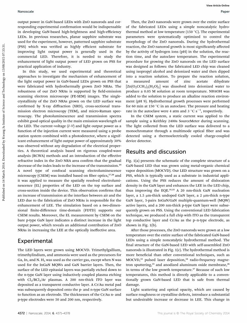
The I–V characteristics were measured using a probe stationequipped with a Keithley 2400s SourceMeter to characterize theelectrical properties of the GaN-based LED with ZnO NRAs. To
measure the I–V curve, we have removed ZnO NRAs on themetalpad by simple scratching method. Fig. 3(a) presents the I–Vcharacteristics of the LED with (lled square) and without ZnONRAs (opened square). As shown in the gure, both plotsexhibit good diode responses with a driving current of 20 mA inan operating voltage of approximately 3.8 V, which conse-quently indicates an acceptable electrical performance. Moreimportantly, the two curves are almost identical to each otherthroughout the entire observation voltage, which is a clearsignature that the electrical properties are not damaged by theZnO NRA fabrication. This result is a distinct merit of ourhydrothermal method that is operable at lower temperaturesthan other methods.14
Fig. 3(b) presents the light output power as a function of theinjection current for the LEDs with and without ZnO NRAs. Thelight output power from the LED with ZnO NRAs was approxi-mately 30% greater than that from the LED without ZnO NRAsat an operating current of 20 mA. This value is remarkable sincewe have used commercially optimized epilayers with PSS whichreadily shows higher light output power. The insets (i) and (ii)are photographs of LED emission at an injection current of 5mA with and without ZnO NRAs, respectively. Considering thatthe electrical property does not change, such enhancement ofthe light output power is attributed to the increased LEE of theLED structure with ZnO NRAs.
To explain the enhancement of the light output power, weemployed the effective refractive index based on effectivemedium theory. Effective medium theory is a physical model
Fig. 3 Electrical properties and light output power as a function of theinjection current of the GaN-based LED, (a) the current vs. voltagecurves and (b) the amount of light output power as a function of theinjection current for GaN-based LEDs with and without ZnO nanorodarrays. The insets show emission images of (i) conventional and (ii)ZnO-nanorod-arranged LED at an injection current of 5 mA.
4374 | Nanoscale, 2014, 6, 4371–4378
that describes the macroscopic properties of a medium, wherethe refractive index of the composite is the weighted average ofeach component scaled by its volume fraction. If the electro-magnetic-radiation wavelength is considerably larger than thenanostructure size, the classical theories of inhomogeneousmedia presume that the material can be treated as a homoge-neous substance with an effective dielectric function andrefractive index. These quantities depend on the properties ofthe constituents and their volume fractions and sizes.34,35
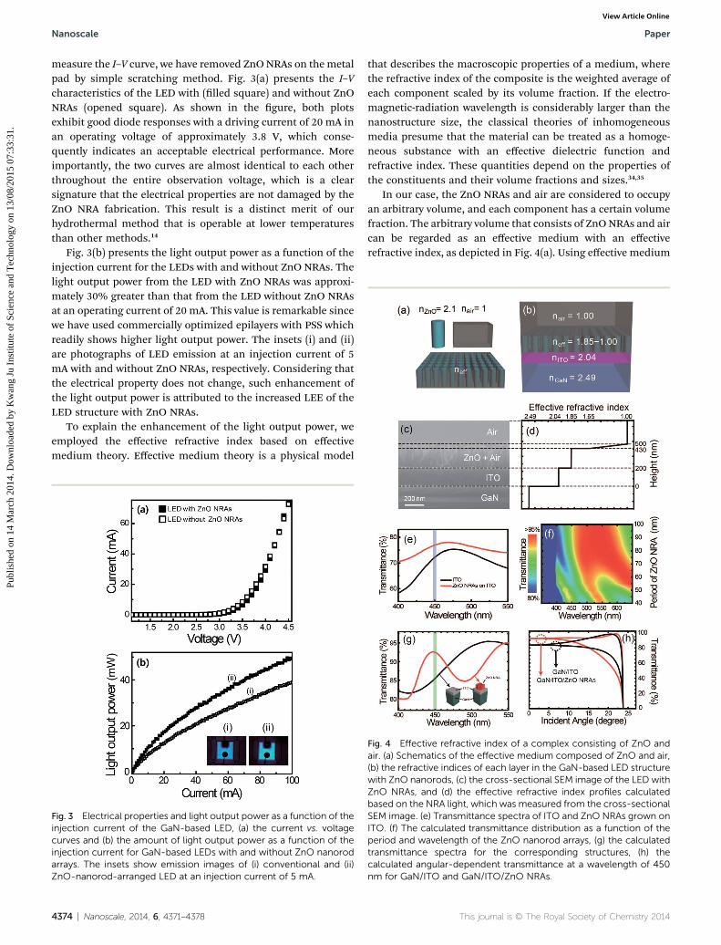
In our case, the ZnO NRAs and air are considered to occupyan arbitrary volume, and each component has a certain volumefraction. The arbitrary volume that consists of ZnO NRAs and aircan be regarded as an effective medium with an effectiverefractive index, as depicted in Fig. 4(a). Using effective medium
Fig. 4 Effective refractive index of a complex consisting of ZnO andair. (a) Schematics of the effective medium composed of ZnO and air,(b) the refractive indices of each layer in the GaN-based LED structurewith ZnO nanorods, (c) the cross-sectional SEM image of the LED withZnO NRAs, and (d) the effective refractive index profiles calculatedbased on the NRA light, which was measured from the cross-sectionalSEM image. (e) Transmittance spectra of ITO and ZnO NRAs grown onITO. (f) The calculated transmittance distribution as a function of theperiod and wavelength of the ZnO nanorod arrays, (g) the calculatedtransmittance spectra for the corresponding structures, (h) thecalculated angular-dependent transmittance at a wavelength of 450nm for GaN/ITO and GaN/ITO/ZnO NRAs.
theory, the effective refractive index neff of the ZnO NRAs and airis calculated as
neff ¼ [nZnO2fZnO + nair
2(1 � fZnO)]1/2 (1)
where fZnO is the volume fraction of ZnO and nZnO and nair arethe refractive indices of ZnO and air, respectively.33 The refrac-tive indices of GaN, ITO, and ZnO are approximately 2.49, 2.04,and 2.11, respectively, at a wavelength of 450 nm, whichcorresponds to the LED emission wavelength.36 In ZnO NRAlayer, the effective refractive index was approximated to varyfrom 1.85–1.00, depending on the volume fraction variationcaused by an inhomogeneous length of the ZnO nanorods. Theresultant effective refractive indices of each layer in the LEDwith ZnO NRAs are illustrated in Fig. 4(b). Clearly, the refractiveindices tend to decrease from the GaN layer to air because of thepresence of ZnO NRAs. In a conventional LED, the indexcontrast between the ITO top layer and air is as large as 1.04.However, if the top layer changes to an effective mediumcomposed of ZnO NRAs and air, the index contrast becomesnegligibly small because the ZnO NRAs form a graded refractiveindex (GRIN) layer. The small index difference between the LEDtop layer and air induces an enhanced LEE because of theincreased photon escape cone angle and increased trans-mittance at the interface.
Fig. 4(c) presents the cross-sectional SEM image of ZnONRAs that were grown on the LED with an ITO top contact layer.Because the measured deviation of the length of the ZnOnanorods is approximately 70 nm, the volume fraction of ZnOchanges from �80% to 0% along the vertical direction towardthe top surface of the LEDs. Fig. 4(d) presents the modeledeffective refractive index as a function of the LED heightaccording to the volume fraction variations shown in Fig. 4(c).To attribute the length deviation of ZnO NRAs, we separatedZnO NRA layer into two sub-layers. The rst layer at a heightfrom 200 nm to 430 nm measured from the GaN/ITO interfacehas constant volume fraction of 80%, which corresponds to neff¼ 1.85. In the second layer at a height from 430 nm to 500 nm,we modeled that the volume fraction of the ZnO NRAs graduallyvaries from 50% to 0%. This model qualitatively coincides withthe cross-sectional SEM image depicted in Fig. 4(c). Thesegradual decreases in the refractive index cause easier photonescape from the devices in a manner that is correlated with theincreased amount of transmission at the LED–air interface. It isobvious that ZnO NRAs act as GRIN materials which lead to anincrease in the LEE of the LED.
The transmission spectra of the bare ITO layer and thosecombined with ZnO NRAs are experimentally obtained toconrm such effect. These transmittance spectra are plotted inFig. 4(e). The transmittances of the bare ITO layer andcombined layer at the 450 nm, which is an emission wavelengthof the GaN-based LED, were 71% and 77%, respectively. Thecombined layer has higher transmittance which indicates thatgraded refractive index introduced by ZnO NRAs positivelycontributes in the LEE.
The transmittance was also calculated as a function ofwavelength and the period of the NRAs by applying the RCWA
method to understand our experiment more thoroughly. Theperiod of the ZnO NRAs was varied from 40 to 100 nm, and theaverage height of the ZnO nanorods was 300 nm with 70 nmdeviation in this calculation. The wavelength of the emittedlight ranged from 350 to 650 nm, and normal incidence wasassumed throughout the entire interfaces. As shown in Fig. 4(f),a clear oscillation of the transmittance as a function of thewavelength is observed, which indicates that thin-lm inter-ference occurs in both the ITO layer and ZnO NRAs. Thisinterference is also affected by the period of ZnO NRAs; theoscillating period increases for larger periods.
In Fig. 4(g), the transmittance that was calculated at normalincidence at a period of 40 nm is represented as a function ofthe wavelength. The LED with ZnO NRAs exhibited a hightransmittance of approximately 93% at the operating wave-lengths of 440–460 nm, whereas the LED without ZnO NRAsexhibited a relatively low transmittance of approximately 85%,which shows a qualitative agreement with experiment. Fig. 4(h)presents the angle-dependent transmittance that was calculatedat the wavelength of 450 nm for the LEDs with and without ZnONRAs. The LED with ZnO NRAs exhibited a higher trans-mittance for both transverse electric and transverse magneticpolarizations than the LED without ZnONRAs over a large rangeof angles to approximately 25�. These simulation results indi-cate that the origin of the enhanced light output is the increasedtransmittance at the LED–air interface via the ZnO NRAs.
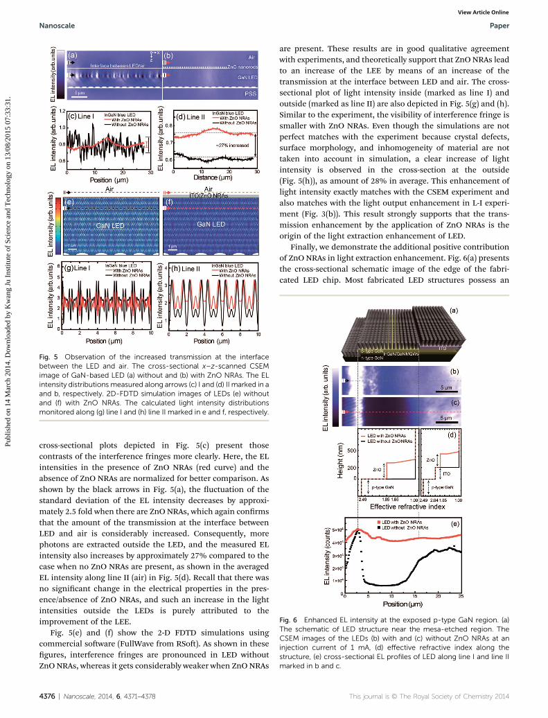
Cross-sectional CSEM was conducted to understand howthis transmission enhancement affects the device performance.Because of the high depth-resolution along the surface-normaldirection of confocal microscopy, the EL through the cross-sectional plane can be mapped from the substrate to the toplayer of the device, as shown in Fig. 5(a) and (b). Fig. 5(a) and (b)present the two-dimensional x–z-scanned CSEM images of theLEDs without and with ZnO NRAs, respectively. The whitedashed lines distinguish each layer: the LED, the ZnO NRAs,and air.
A remarkable feature in Fig. 5(a) is the quasi-periodic,vertically aligned interferometric EL patterns. When reectingat the PSS/LED interface, light is diffracted because the lens-shaped, hexagonally arranged quasi-periodic patterns with anaveraged period of d¼ 2 mm act as an effective two-dimensionaldiffraction grating.37 The lights scattered from this patternedsurface form an interference fringe with an averaged period ofD¼ (D/d)l, where D ¼ 3.5 mm is the distance from the PSS to theMQWs. Considering that l ¼ 450 nm, D is calculated to be 0.8mm, which is consistent with the measured period of interfer-ence fringes. The high visibility of these fringes in the absenceof ZnO NRAs is a clear signature that major populations ofgenerated photon inside the MQWs are reected back and forthbetween the LED–air interface and the PSS/LED interface, andthe amount of extracted photons is considerably low as aresult.38 However, in the presence of ZnO NRAs on top of theLED, those interference fringes are signicantly weakened, asshown in Fig. 5(b). This result strongly indicates that theamount of photons that reect back and forth inside the LEDs issignicantly reduced because the optical properties of the air–LED interface are modied in the presence of ZnO NRAs. The
Fig. 5 Observation of the increased transmission at the interfacebetween the LED and air. The cross-sectional x–z-scanned CSEMimage of GaN-based LED (a) without and (b) with ZnO NRAs. The ELintensity distributions measured along arrows (c) I and (d) II marked in aand b, respectively. 2D-FDTD simulation images of LEDs (e) withoutand (f) with ZnO NRAs. The calculated light intensity distributionsmonitored along (g) line I and (h) line II marked in e and f, respectively.
Fig. 6 Enhanced EL intensity at the exposed p-type GaN region. (a)The schematic of LED structure near the mesa-etched region. TheCSEM images of the LEDs (b) with and (c) without ZnO NRAs at aninjection current of 1 mA, (d) effective refractive index along thestructure, (e) cross-sectional EL profiles of LED along line I and line IImarked in b and c.
Nanoscale Paper
Publ
ishe
d on
14
Mar
ch 2
014.
Dow
nloa
ded
by K
wan
g Ju
Ins
titut
e of
Sci
ence
and
Tec
hnol
ogy
on 1
3/08
/201
5 07
:33:
31.
View Article Online
cross-sectional plots depicted in Fig. 5(c) present thosecontrasts of the interference fringes more clearly. Here, the ELintensities in the presence of ZnO NRAs (red curve) and theabsence of ZnO NRAs are normalized for better comparison. Asshown by the black arrows in Fig. 5(a), the uctuation of thestandard deviation of the EL intensity decreases by approxi-mately 2.5 fold when there are ZnO NRAs, which again conrmsthat the amount of the transmission at the interface betweenLED and air is considerably increased. Consequently, morephotons are extracted outside the LED, and the measured ELintensity also increases by approximately 27% compared to thecase when no ZnO NRAs are present, as shown in the averagedEL intensity along line II (air) in Fig. 5(d). Recall that there wasno signicant change in the electrical properties in the pres-ence/absence of ZnO NRAs, and such an increase in the lightintensities outside the LEDs is purely attributed to theimprovement of the LEE.
Fig. 5(e) and (f) show the 2-D FDTD simulations usingcommercial soware (FullWave from RSo). As shown in thesegures, interference fringes are pronounced in LED withoutZnO NRAs, whereas it gets considerably weaker when ZnO NRAs
4376 | Nanoscale, 2014, 6, 4371–4378
are present. These results are in good qualitative agreementwith experiments, and theoretically support that ZnO NRAs leadto an increase of the LEE by means of an increase of thetransmission at the interface between LED and air. The cross-sectional plot of light intensity inside (marked as line I) andoutside (marked as line II) are also depicted in Fig. 5(g) and (h).Similar to the experiment, the visibility of interference fringe issmaller with ZnO NRAs. Even though the simulations are notperfect matches with the experiment because crystal defects,surface morphology, and inhomogeneity of material are nottaken into account in simulation, a clear increase of lightintensity is observed in the cross-section at the outside(Fig. 5(h)), as amount of 28% in average. This enhancement oflight intensity exactly matches with the CSEM experiment andalso matches with the light output enhancement in L-I experi-ment (Fig. 3(b)). This result strongly supports that the trans-mission enhancement by the application of ZnO NRAs is theorigin of the light extraction enhancement of LED.
Finally, we demonstrate the additional positive contributionof ZnO NRAs in light extraction enhancement. Fig. 6(a) presentsthe cross-sectional schematic image of the edge of the fabri-cated LED chip. Most fabricated LED structures possess an
electrical safety margin area where the bare p-type GaN isexposed. This area typically occupies approximately 10% of thearea of a single chip, which detracts from the overall light-emitting performance. Fig. 6(b) and (c) present the lateral CSEMimage of the LED with and without ZnO NRAs at the edge of anLED chip, respectively, including a mesa-etched region. Asobserved in these gures, ZnO NRAs also enhance the LEE inthis region. Fig. 6(d) presents the effective refractive indexprole along the structure, which introduces the light extractionenhancement also in the electrical safety margin area. A clearsuppression of the EL intensity at the electrical safety marginarea from 2.5 to 16 mm is observed in the absence of ZnO NRAs(see black square in the Fig. 6(e)). On the contrary, in thepresence of ZnO NRAs, the EL intensity is prominentlyincreased by more than 3 times (see the red square in Fig. 6(e)).
An additional remarkable feature is the intense EL emissionat the edge of the mesa-etched region. This prominent emissionis attributed to photons escaping from the side wall of the LEDs.This observation suggests that the enhancement of light outputby ZnO NRAs occurs over the entire LED surface, including theexposed p-type GaN layer, due to the GRIN effect.
Conclusions
We demonstrated the mechanism of enhanced light output inGaN-based LED grown on PSS, that has ZnO NRAs which weregrown by a simple noncatalyzed maskless hydrothermalmethod. Using HR-TEM, micro-Raman spectroscopy, andmacro-PL spectroscopy, the hydrothermally grown ZnO nano-rods were veried to have high crystalline quality and goodoptical properties. The amount of light output power from theLED with ZnO NRAs was improved by approximately 30%compared to the conventional LED without ZnO NRAs, whereasthe electrical properties of ZnO NRAs were not signicantlyaffected. The effective medium theory was applied to explain therole of ZnO NRAs to such enhancement. The cross-sectionalCSEM images suggest that the light output is enhanced becauseof the increased transmission at the ITO/air interface. Suchobservation is supported by the calculations based on FDTDmethod combined with the effective medium theory. Theenhancement of EL intensity in the electrical safety margin areawith ZnO NRAs is also veried using CSEM. We believe that ourresults clearly explain the role of ZnO NRAs for light extractionenhancement on GaN-based LEDs and pave the way to high-brightness, high-efficiency GaN-based LEDs.
Acknowledgements
This work was supported by the Institute for Basic Science(EM1304) in Korea.
Notes and references
1 E. F. Schubert and J. K. Kim, Science, 2005, 308, 1274–1278.2 A. Zukauskas, M. S. Shur and R. Gaska, Introduction to Solid-State Light, vol. 1, Wiley & Sons, New York, 2002.
3 K. Okamoto and Y. Kawakami, IEEE J. Sel. Top. QuantumElectron., 2009, 15, 1199–1209.
4 S. Pimputkar, J. S. Speck, S. P. DenBaars and S. Nakamura,Nat. Photonics, 2009, 3, 180–182.
5 E. Homeyer, P. Mattila, J. Oksanen, T. Sadi, H. Nykanen,S. Suihkonen, C. Symonds, J. Tulkki, F. Tuomisto,M. Sopanen and J. Bellessa, Appl. Phys. Lett., 2013, 102,081110–081114.
6 J. H. Son, J. U. Kim, Y. H. Song, B. J. Kim, C. J. Ryu andJ.-L. Lee, Adv. Mater., 2012, 24, 2259–2262.
7 J. K. Kim, S. Chhajed, M. F. Schubert, E. F. Schubert,A. J. Fischer, M. H. Crawford, J. Cho, H. Kim and C. Sone,Adv. Mater., 2008, 20, 801–804.
9 D.-H. Kim, C.-O. Cho, Y.-G. Roh, H. Jeon, Y. S. Park, J. Cho,J. S. Im, C. Sone, Y. Park, W. J. Choi and Q. H. Park, Appl.Phys. Lett., 2005, 87, 203508.
10 A. Chen, S. J. Chua, P. Chen, X. Y. Chen and L. K. Jian,Nanotechnology, 2006, 17, 3903–3908.
11 K.-J. Byeon, S.-Y. Hwang and H. Lee, Appl. Phys. Lett., 2007,91, 091106.
12 X. A. Cao, S. J. Pearton, A. P. Zhang, G. T. Dang, F. Ren,R. J. Shul, L. Zhang, R. Hickman and J. M. Van Hove, Appl.Phys. Lett., 1999, 75, 2569–2571.
13 J. Zhong, H. Chen, G. Saraf, Y. Lu, C. K. Choi, J. J. Song,D. M. Mackie and H. Shen, Appl. Phys. Lett., 2007, 90, 203515.
14 S. J. An, J. H. Chae, G.-C. Yi and G. H. Park, Appl. Phys. Lett.,2008, 92, 121108.
15 K.-K. Kim, S.-d. Lee, H. Kim, J.-C. Park, S.-N. Lee, Y. Park,S.-J. Park and S.-W. Kim, Appl. Phys. Lett., 2009, 94, 071118.
16 H. Park, K.-J. Byeon, K.-Y. Yang, J.-Y. Cho and H. Lee,Nanotechnology, 2010, 21, 355304.
17 K. S. Kim, S.-M. Kim, H. Jeong, M. S. Jeong and G. Y. Jung,Adv. Funct. Mater., 2010, 20, 1076–1082.
18 B.-U. Ye, B. J. Kim, Y. H. Song, J. H. Son, H. k. Yu, M. H. Kim,J.-L. Lee and J. M. Baik, Adv. Funct. Mater., 2012, 22, 632–639.
19 J. W. Leem, Y. Yeh and J. S. Yu, Opt. Express, 2012, 20, 4056–4066.
20 H. Jeong, T. S. Oh, Y. S. Lee, H. G. Kim, C.-H. Hong,E.-K. Suh, O. H. Cha, H. S. Lee and M. S. Jeong, J. Phys. D:Appl. Phys., 2011, 44, 505102.
21 H. Xiao-Hui, L. Jian-Ping, F. Ya-Ying, K. Jun-Jie, H. Yang andW. Huai-Bing, IEEE Photonics Technol. Lett., 2011, 23, 944–946.
22 Y. B. Tao, T. J. Yu, Z. Y. Yang, D. Ling, Y. Wang, Z. Z. Chen,Z. J. Yang and G. Y. Zhang, J. Cryst. Growth, 2011, 315, 183–187.
23 J. J. Wu and D. K. P. Wong, Adv. Mater., 2007, 19, 2015–2019.24 Y. Shen, J.-I. Hong, S. Xu, S. Lin, H. Fang, S. Zhang, Y. Ding,
R. L. Snyder and Z. L. Wang, Adv. Funct. Mater., 2010, 20,703–707.
25 Y. J. Fang, J. Sha, Z. L. Wang, Y. T. Wan, W. W. Xia andY. W. Wang, Appl. Phys. Lett., 2011, 98, 033103.
26 H. Chik, J. Liang, S. G. Cloutier, N. Kouklin and J. M. Xu,Appl. Phys. Lett., 2004, 84, 3376–3378.
27 J. H. Kim, D. Andeen and F. F. Lange, Adv. Mater., 2006, 18,2453–2457.
28 H.-K. Fu, C.-L. Cheng, C.-H. Wang, T.-Y. Lin and Y.-F. Chen,Adv. Funct. Mater., 2009, 19, 3471–3475.
29 U. Ozgur, Y. I. Alivov, C. Liu, A. Teke, M. A. Reshchikov,S. Dogan, V. Avrutin, S. J. Cho and H. Morkoc, J. Appl.Phys., 2005, 98, 041301.
30 S. H. Jung, E. Oh, K. H. Lee, W. Park and S. H. Jeong, Adv.Mater., 2007, 19, 749–753.
31 S. K. Mohanta, S. Tripathy, X. H. Zhang, D. C. Kim, C. B. Soh,A. M. Yong, W. Liu and H. K. Cho, Appl. Phys. Lett., 2009, 94,041901–041903.
32 F. K. Shan, G. X. Liu, W. J. Lee and B. C. Shin, J. Appl. Phys.,2007, 101, 053106–053108.
4378 | Nanoscale, 2014, 6, 4371–4378
33 V. A. Fonoberov, K. A. Alim, A. A. Balandin, F. Xiu and J. Liu,Phys. Rev. B: Condens. Matter Mater. Phys., 2006, 73, 165317.
34 Y. Ono, Y. Kimura, Y. Ohta and N. Nishida, Appl. Opt., 1987,26, 1142–1146.
35 T. C. Choy, Effective Medium Theory, Principles andApplication, Oxford University Press Inc., Oxford, 1999.
36 M. Bass, C. DeCuastis, J. Enoch, V. Lakshminarayanan, G. Li,C. MacDonald, V. Mahajan and E. V. Stryland, Handbook ofOptics, McGraw-Hill Professional, New York, 3rd edn, 2009.
37 S.-M. Kim, K. S. Kim, G. Y. Jung, J. H. Baek, H. Jeong andM. S. Jeong, J. Phys. D: Appl. Phys., 2009, 42, 152004.
38 H. W. Choi, C. Liu, E. Gu, G. McConnell, J. M. Girkin,I. M. Watson and M. D. Dawson, Appl. Phys. Lett., 2004, 84,2253–2255.