Page 1
Nanoscale investigation on large crystallites in TiO2 nanotubearrays and implications for high-quality hybrid photodiodes
Andreas Wisnet • Markus Thomann •
Jonas Weickert • Lukas Schmidt-Mende •
Christina Scheu
Received: 26 January 2012 / Accepted: 14 May 2012 / Published online: 30 May 2012
� Springer Science+Business Media, LLC 2012
Abstract Anodized TiO2 nanotube arrays fabricated on a
TiO2 thin film on conducting glass substrates can be readily
implemented in diverse applications like hybrid solar cells.
In this study, we concentrate on morphologies with inner
tube diameter being around 30 nm which is in dimension
of the exciton diffusion length of common organic hole
conductors. Cross-sectional preparation of the intact tube
array in correlation with transmission electron microscopy
has been performed to get local information on the TiO2
nanotubes and their arrangements, depending on anodiza-
tion voltage. Crystallites have been found to be anatase and
in size of several hundred nanometers along tube walls
with increasing length for increasing anodization voltages.
Inter-tube connections with similar crystal orientations of
adjacent tubes are found. These give rise to large areas of
uniform orientation. Thus, the number of grain boundaries
within the film is low compared to the reported values for
different TiO2-polymer material systems. Using the arrays,
hybrid TiO2 solar cells were fabricated, which show high
fill factors indicating good electron transport. The results
suggest high electron mobility and are encouraging for a
utilization of the nanotube arrays in next generation
photovoltaics.
Introduction
TiO2 is a versatile metal oxide which has tunable optical
and electronic properties depending on its different struc-
tures and can be produced by various fabrication routes. In
recent years, several fields of application are more and
more using nanostructured TiO2, often to maximize surface
areas and accordingly interface areas when combined with
other materials [1]. A few very important examples are the
anodized TiO2 nanotube arrays, among others used in thin-
film solar cells; [2–8], lithium-ion batteries [9]; hydrogen
sensors [10, 11]; and water photolysis [12, 13]. A conse-
quence of downsizing structures is the change in their
physical and chemical properties, which again cause
modification of important electronic properties, especially
the mobility of electrons along and between tubes [1].
In this regard, electron trap states have been identified to be
a limiting factor [14]. TiO2 nanotube arrays have been
analyzed via intensity-modulated photocurrent and inten-
sity-modulated photovoltage spectroscopy, and the elec-
trons’ crossing at grain boundaries was found to be
severely affected by these trap states. Hence, large crys-
tallites along the tubes are surmised to facilitate excellent
electron transport [15, 16].
The present study aims at an elucidation of the material
properties of anodized nanotubes forming an array on
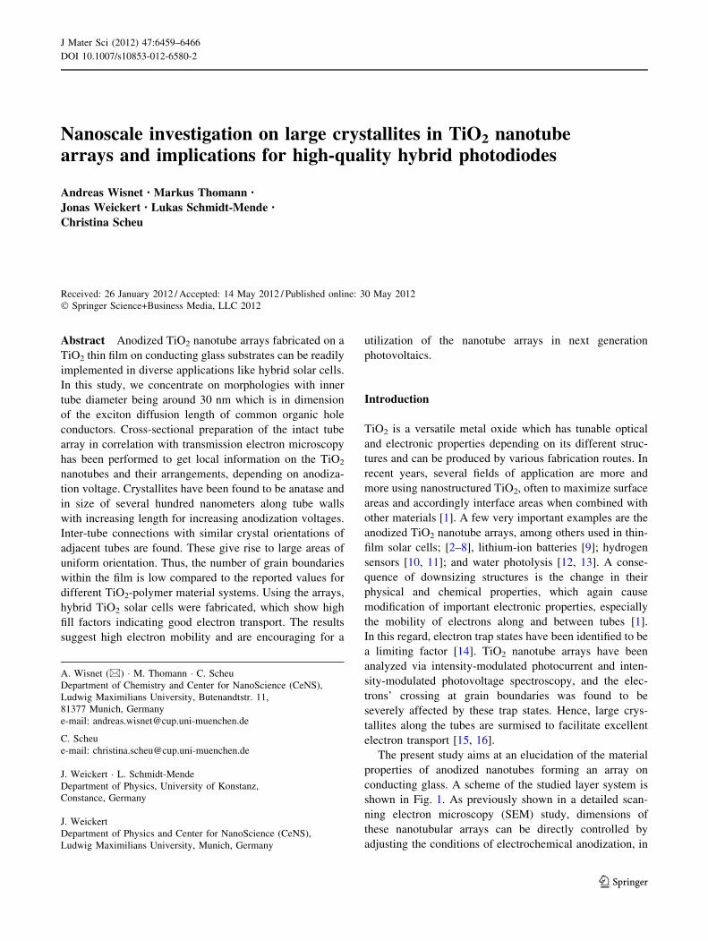
conducting glass. A scheme of the studied layer system is
shown in Fig. 1. As previously shown in a detailed scan-
ning electron microscopy (SEM) study, dimensions of
these nanotubular arrays can be directly controlled by
adjusting the conditions of electrochemical anodization, in
A. Wisnet (&) � M. Thomann � C. Scheu
Department of Chemistry and Center for NanoScience (CeNS),
Ludwig Maximilians University, Butenandtstr. 11,
81377 Munich, Germany
e-mail: [email protected]
C. Scheu
e-mail: [email protected]
J. Weickert � L. Schmidt-Mende
Department of Physics, University of Konstanz,
Constance, Germany
J. Weickert
Department of Physics and Center for NanoScience (CeNS),
Ludwig Maximilians University, Munich, Germany
123
J Mater Sci (2012) 47:6459–6466
DOI 10.1007/s10853-012-6580-2
Page 2
particular, the anodization bath temperature and the anod-
ization voltage [17]. Four different voltages (10, 15, 20,
and 25 V) have been applied during fabrication. They were
chosen to receive inner tube diameters of around 30 nm,
which is in the order of dimension of the exciton diffusion
length in semiconducting polymers like poly(3-hexylthi-
ophene) (P3HT) [18], rendering them particularly inter-
esting for applications in solid-state dye-sensitized hybrid
solar cells. Since an anodization voltage of 10 V resulted in
a partially dissolved array composed of damaged tubes, it
is not studied further.
Up to now, SEM and X-ray diffraction (XRD) were used
as standard analysis methods for TiO2 nanotube arrays,
while transmission electron microscopy (TEM) has been
applied on single nanotubes or dissolved arrays [15, 19–
21]. In this study, TEM has been chosen as primary method
for analysis to gain local information about tube mor-
phology, phase purity, crystal grain size, and crystal ori-
entation within the tubes in context of the intact array. The
results are correlated to properties by fabricating hybrid
solar cells composed of the TiO2 nanotube arrays, a com-
mon ruthenium dye and P3HT. This design is adequate to
gain basic information while maintaining simplicity and
comparability, so that results can be appraised in the con-
text of already existing studies. Current–voltage measure-
ments have been carried out to characterize electronic
behavior, with a focus on the fill factor which is influenced
by electron mobility and charge recombination.
Experimental section
TiO2 nanotubes were synthesized on tin-doped indium
oxide (ITO)-coated glass substrates. ITO substrates were
successively cleaned in ultrasonic baths of acetone and
isopropanol for 30 min each, dried in N2 stream and sub-
jected to a 7-min cleaning in an O2 plasma. Substrates were
transferred to the main chamber of a NanoSystems Gamma
1000C sputter system with a base pressure of
3 9 10-8 Torr. Approximately, 40 nm TiO2 and 400 nm
Ti were DC sputtered at 500 �C and Ar gas pressures of 5
and 4 m Torr, respectively. Samples were anodized in an
ethylene glycol-based electrolyte containing 0.4 wt%
NH4F and 2 vol% deionized water. Anodizations were
carried out in a two-electrode setup versus a Pt counter
electrode at room temperature and different anodization
voltages. Anodization was stopped after complete con-
sumption of the Ti feed substrate, but before corrosion of
the underlying ITO as described elsewhere [17]. After
anodization, samples were excessively rinsed with EtOH,
slowly dried in air and annealed on a hotplate at 450 �C in
ambient air for 1 h with heating and cooling rates of 5 and
2.5 �C/min, respectively.
TEM cross-sectional specimens have been prepared
via standard route by gluing a sandwich of the layers
into a brass tube, cutting of slices, grinding, dimpling,
and ion milling according to Strecker et al. [22]. For
TEM investigation, a Jeol JEM 2011 operated at 200 kV
and a FEI Titan (S)TEM 80–300 operated at 300 kV
have been used. The Titan is equipped with an EDAX
detector for energy dispersive X-ray analysis. Off-axis
dark-field (DF) images have been taken without use of
beam-tilting.
Hybrid solar cells were fabricated based on TiO2
nanotube arrays anodized at 25 V as described above. The
anodized and annealed nanotubes of 500–600 nm length
were immersed for 18 h in a 0.4 mM ethanol solution of
the ruthenium dye Z907 [23]. Subsequently, samples were
rinsed with ethanol and dried in ambient air. P3HT was
deposited on top of the nanostructures as hole conductor. It
was prepared as a 30 mg/ml solution in chlorobenzene and
spin coated at 1200 rpm for 1 min after leaving the solu-
tion on the substrate for 2 min to achieve sufficient wetting
of the nanotubes. Immediately after spin coating, the films
were annealed at 150 �C for 1 min in ambient air. Then, a
*50 nm thick layer of poly(3,4-ethylenedioxythiophene)–
polystyrene sulfonic acid (PEDOT:PSS) was spray-depos-
ited onto the P3HT as described previously [24]. In brief,
PEDOT:PSS was diluted in 2-propanol at a ratio of 1:10
and the substrate was wetted with the solution via spraying.
Subsequently, the film was spin coated at 800 rpm for
1 min. Solar cells were finalized by DC sputtering Ag top
contacts through a shadow mask, resulting in an active area
of 0.125 cm2.
Solar cells were tested in the dark and under illumina-
tion with a LOT-Oriel LS0106 AM 1.5 g solar simulator.
The light intensity was adjusted to 100 mW/cm2 with a
Fraunhofer Institute certified Si solar cell as a reference.
Current density–voltage (I–V) characteristics were recor-
ded using a Keithley Sourcemeter 2400 controlled by a
self-written LabView program.
Fig. 1 Scheme of the sample. The nanotubes are composed of
anatase, while the TiO2 flat film has rutile structure. ITO was used as
conducting glass (Color figure online)
6460 J Mater Sci (2012) 47:6459–6466
123
Page 3
Results
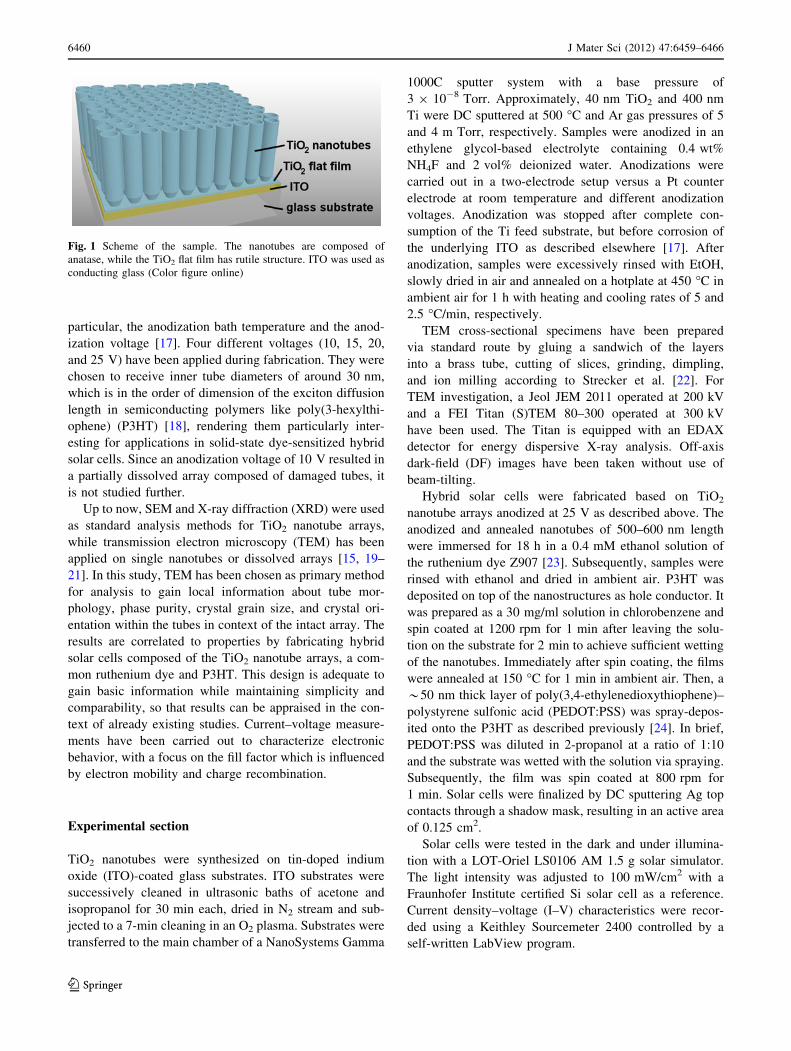
Bright-field (BF) overview images were taken to get
information about the tube length, ranging from 475 to
575 nm for increasing voltage (Fig. 2). The values are in
accordance to the results from SEM analysis, which has
been performed earlier, although the tube length at the
15 V sample is slightly larger than expected [17]. The
increasing length at higher anodization voltages could be
confirmed. Wall thicknesses have been measured in
slightly higher magnified BF images (not shown) and result
in averages of 9 (±1), 9 (±2) and 12 (±2) nm for 15, 20
and 25 V anodization voltages, respectively. Owing to the
sample thickness, pore diameters were hardly distinguish-
able, but exemplary areas showed inner diameters of
around 30 nm for all anodization voltages with a slight
tendency to increase at higher voltages. Energy dispersive
X-ray analysis (not shown) exhibits that the tubes contain
mainly titanium and oxygen, with some traces of sodium in
all samples and calcium in the 15 V sample only, which are
probably residues from the sample preparation.
For a better understanding of electronic behavior, fur-
ther investigation of the crystalline structure and phases
was performed. Electron diffraction (ED) patterns show
polycrystalline anatase. At specific areas, DF images were
taken to determine crystal sizes. Figure 3 shows BF ima-
ges, their corresponding ED patterns and DF images. The
ED patterns, which have been taken at circular areas of
about 650 nm diameter, show distinguishable major
reflections in all cases, contrary to ring-like structures
which would have been expected for fully polycrystalline
samples. In accordance, the DF images taken with the
indicated (200), (101) and (101) reflections of anatase
confirm that a large grain size along the tube wall and a
similar orientation over several nanotubes is present. Thus,
although these areas show no single crystal, they appear to
be composed of larger grains (including slight rotations)
and some smaller grains filled in between.
The crystalline appearance along the tube walls is
assumed to be one of the most important features allowing
a high conductivity parallel to the tube axis. For the present
samples, the results indicate that the grain size along this
axis is several 100 nm for individual tubes. These large
crystals can only be distinguished when they are oriented
near a zone axis and were observed at various positions
within the sample. Groups of nanotubes with similar crystal
orientation extend up to 500 nm in diameter, like the one
shown in Fig. 3c. Thus, adjacent tubes often appear with
the same orientation.
BF images typically show Moire patterns in wide areas,
which indicate crystallites slightly rotated by few degrees
against each other. Since reflections with nearly similar
angle cannot be separated by the objective aperture in ED
patterns, these overlapping grains contribute to DF images,
resulting in Moire patterns here as well. Owing to their
appearance in clearly distinguishable nanotubes, like the
one marked by an arrow in Fig. 3c, it is assumed that the
crystals of the transmitted front and back tube walls are
slightly rotated with respect to each other. In addition to
these findings, a trend toward developing a larger grain size
at higher anodization voltages is observable. The mean
lengths of the 10 largest crystals found for each voltage are
210 nm (160–260 nm; 15 V), 260 nm (230–310 nm;
20 V), and 320 nm (250–360 nm; 25 V).
For establishing further proof of the large crystal size,
series of HRTEM micrographs have been captured at
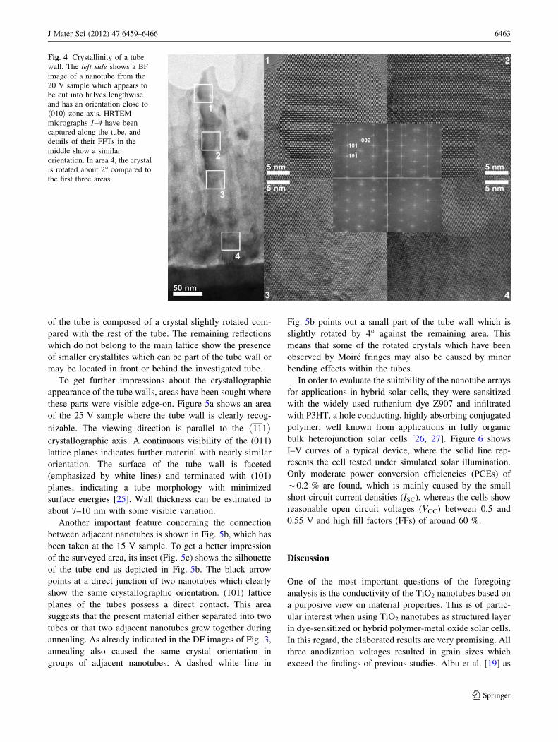
various tubes. An exemplary one is given in Fig. 4. The left
BF image shows large parts of a nanotube which has been
cut at the top during ion milling. Its darker appearance
hints at an orientation parallel to a zone axis. At the closed
end just below box 4, Moire patterns are visible again, and
so nearly similar crystal orientations are present. Boxes
numbered from 1 to 4 are set at the positions where the
corresponding HRTEM micrographs, shown at the right
side of Fig. 4, have been taken. At all the four positions,
the lattice planes indexed as (101), 101� �
and (002) are
clearly visible, resulting in a view along the h010i zone
axis. Owing to the thickness of the sample, the quality of
their appearance is decreasing from top to bottom, or 1 to 4,
respectively. For further illustration of the similar crystal-
line orientation, fast fourier transforms (FFTs) have been
calculated from images 1 to 4. Their center details are
shown as insets in the HRTEM images. Apart from their
similarity, two features deserve attention:
First, the FFT in image 2 shows spots adjacent to (002)
and its related reflections. This is attributed to the slightly
rotated area at the left side of the HRTEM image which is
Fig. 2 Comparison of TiO2 tube length of three samples anodized at
different voltages. Higher voltages lead to increasing length. Note the
gold particles stemming from SEM characterization at the top of the
20 and 25 V samples
J Mater Sci (2012) 47:6459–6466 6461
123
Page 4
partly hidden by the FFT inset. As it is visible in the BF
image, this part is near the edge of the nanotube, which
points toward some changes in crystal orientation in this
part of the tube wall. The second interesting feature is
visible when comparing the FFT of image 4 to the other
three FFTs. It is rotated by 2�, which means that the bottom
Fig. 3 BF (left) and DF (right) images show typical grains found in
samples anodized at 15 V (a, b), 20 V (c, d), and 25 V (e, f). The arrowin image c shows that the sample has been cut at this position.
Corresponding ED patterns are given as insets in the BF images and the
reflections which have been taken for the according DF image, namely
(200) (15 V), (101) (20 V) and (101) (25 V) of anatase, are marked.
Crystals which are slightly rotated to each other, but whose reflections
still lie within the aperture, appear bright in the DF image. Moire patterns
are visible here, too. Selected area diffraction aperture for ED patterns
corresponds to a sample area of about 0.3 lm2 (Color figure online)
6462 J Mater Sci (2012) 47:6459–6466
123
Page 5
of the tube is composed of a crystal slightly rotated com-
pared with the rest of the tube. The remaining reflections
which do not belong to the main lattice show the presence
of smaller crystallites which can be part of the tube wall or
may be located in front or behind the investigated tube.
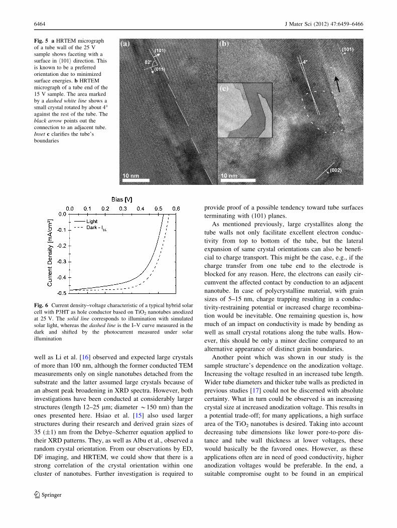
To get further impressions about the crystallographic
appearance of the tube walls, areas have been sought where
these parts were visible edge-on. Figure 5a shows an area
of the 25 V sample where the tube wall is clearly recog-
nizable. The viewing direction is parallel to the 111� �
crystallographic axis. A continuous visibility of the (011)
lattice planes indicates further material with nearly similar
orientation. The surface of the tube wall is faceted
(emphasized by white lines) and terminated with (101)
planes, indicating a tube morphology with minimized
surface energies [25]. Wall thickness can be estimated to
about 7–10 nm with some visible variation.
Another important feature concerning the connection
between adjacent nanotubes is shown in Fig. 5b, which has
been taken at the 15 V sample. To get a better impression
of the surveyed area, its inset (Fig. 5c) shows the silhouette
of the tube end as depicted in Fig. 5b. The black arrow
points at a direct junction of two nanotubes which clearly
show the same crystallographic orientation. (101) lattice
planes of the tubes possess a direct contact. This area
suggests that the present material either separated into two
tubes or that two adjacent nanotubes grew together during
annealing. As already indicated in the DF images of Fig. 3,
annealing also caused the same crystal orientation in
groups of adjacent nanotubes. A dashed white line in
Fig. 5b points out a small part of the tube wall which is
slightly rotated by 4� against the remaining area. This
means that some of the rotated crystals which have been
observed by Moire fringes may also be caused by minor
bending effects within the tubes.
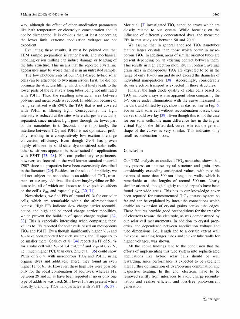
In order to evaluate the suitability of the nanotube arrays
for applications in hybrid solar cells, they were sensitized
with the widely used ruthenium dye Z907 and infiltrated
with P3HT, a hole conducting, highly absorbing conjugated
polymer, well known from applications in fully organic
bulk heterojunction solar cells [26, 27]. Figure 6 shows
I–V curves of a typical device, where the solid line rep-
resents the cell tested under simulated solar illumination.
Only moderate power conversion efficiencies (PCEs) of
*0.2 % are found, which is mainly caused by the small
short circuit current densities (ISC), whereas the cells show
reasonable open circuit voltages (VOC) between 0.5 and
0.55 V and high fill factors (FFs) of around 60 %.
Discussion
One of the most important questions of the foregoing
analysis is the conductivity of the TiO2 nanotubes based on
a purposive view on material properties. This is of partic-
ular interest when using TiO2 nanotubes as structured layer
in dye-sensitized or hybrid polymer-metal oxide solar cells.
In this regard, the elaborated results are very promising. All
three anodization voltages resulted in grain sizes which
exceed the findings of previous studies. Albu et al. [19] as
Fig. 4 Crystallinity of a tube
wall. The left side shows a BF
image of a nanotube from the
20 V sample which appears to
be cut into halves lengthwise
and has an orientation close to
h010i zone axis. HRTEM
micrographs 1–4 have been
captured along the tube, and
details of their FFTs in the
middle show a similar
orientation. In area 4, the crystal
is rotated about 2� compared to
the first three areas
J Mater Sci (2012) 47:6459–6466 6463
123
Page 6
well as Li et al. [16] observed and expected large crystals
of more than 100 nm, although the former conducted TEM
measurements only on single nanotubes detached from the
substrate and the latter assumed large crystals because of
an absent peak broadening in XRD spectra. However, both
investigations have been conducted at considerably larger
structures (length 12–25 lm; diameter *150 nm) than the
ones presented here. Hsiao et al. [15] also used larger
structures during their research and derived grain sizes of
35 (±1) nm from the Debye–Scherrer equation applied to
their XRD patterns. They, as well as Albu et al., observed a
random crystal orientation. From our observations by ED,
DF imaging, and HRTEM, we could show that there is a
strong correlation of the crystal orientation within one
cluster of nanotubes. Further investigation is required to
provide proof of a possible tendency toward tube surfaces
terminating with (101) planes.
As mentioned previously, large crystallites along the
tube walls not only facilitate excellent electron conduc-
tivity from top to bottom of the tube, but the lateral
expansion of same crystal orientations can also be benefi-
cial to charge transport. This might be the case, e.g., if the
charge transfer from one tube end to the electrode is
blocked for any reason. Here, the electrons can easily cir-
cumvent the affected contact by conduction to an adjacent
nanotube. In case of polycrystalline material, with grain
sizes of 5–15 nm, charge trapping resulting in a conduc-
tivity-restraining potential or increased charge recombina-
tion would be inevitable. One remaining question is, how
much of an impact on conductivity is made by bending as
well as small crystal rotations along the tube walls. How-
ever, this should be only a minor decline compared to an
alternative appearance of distinct grain boundaries.
Another point which was shown in our study is the
sample structure’s dependence on the anodization voltage.
Increasing the voltage resulted in an increased tube length.
Wider tube diameters and thicker tube walls as predicted in
previous studies [17] could not be discerned with absolute
certainty. What in turn could be observed is an increasing
crystal size at increased anodization voltage. This results in
a potential trade-off; for many applications, a high surface
area of the TiO2 nanotubes is desired. Taking into account
decreasing tube dimensions like lower pore-to-pore dis-
tance and tube wall thickness at lower voltages, these
would basically be the favored ones. However, as these
applications often are in need of good conductivity, higher
anodization voltages would be preferable. In the end, a
suitable compromise ought to be found in an empirical
Fig. 5 a HRTEM micrograph
of a tube wall of the 25 V
sample shows faceting with a
surface in h101i direction. This
is known to be a preferred
orientation due to minimized
surface energies. b HRTEM
micrograph of a tube end of the
15 V sample. The area marked
by a dashed white line shows a
small crystal rotated by about 4�against the rest of the tube. The
black arrow points out the
connection to an adjacent tube.
Inset c clarifies the tube’s
boundaries
Fig. 6 Current density–voltage characteristic of a typical hybrid solar
cell with P3HT as hole conductor based on TiO2 nanotubes anodized
at 25 V. The solid line corresponds to illumination with simulated
solar light, whereas the dashed line is the I–V curve measured in the
dark and shifted by the photocurrent measured under solar
illumination
6464 J Mater Sci (2012) 47:6459–6466
123
Page 7
way, although the effect of other anodization parameters
like bath temperature or electrolyte concentration should
not be disregarded. It is obvious that, at least concerning
the lower limit, extreme anodization voltages are not
expedient.
Evaluating these results, it must be pointed out that
TEM sample preparation is rather harsh, and mechanical
handling or ion milling can induce damage or bending of
the tube structure. This means that the reported crystalline
appearance may be worse than it is in an untreated sample.
The low photocurrents of our P3HT-based hybrid solar
cells can be attributed to two main issues. First, we did not
optimize the structure filling, which most likely leads to the
lower parts of the relatively long tubes being not infiltrated
with P3HT. Thus, the resulting interfacial area between
polymer and metal oxide is reduced. In addition, because of
being sensitized with Z907, the TiO2 that is not covered
with P3HT is filtering light. Consequently, the light
intensity is reduced at the sites where charges are actually
separated, since incident light goes through the lower part
of the nanotubes first. Second, more importantly, the
interface between TiO2 and P3HT is not optimized, prob-
ably resulting in a comparatively low exciton-to-charge
conversion efficiency. Even though Z907 has proven
highly efficient in solid-state dye-sensitized solar cells,
other sensitizers appear to be better suited for applications
with P3HT [23, 28]. For our preliminary experiments,
however, we focused on the well-known standard material
Z907 since its properties have been extensively described
in the literature [29]. Besides, for the sake of simplicity, we
did not subject the nanotubes to an additional TiCl4 treat-
ment or use any additives like 4-tert-butylpyridine or lith-
ium salts, all of which are known to have positive effects
on the cell’s VOC and especially ISC [30, 31].
Nevertheless, we find FFs of around 60 % for our solar
cells, which are remarkable within the aforementioned
context. High FFs indicate slow charge carrier recombi-
nation and high and balanced charge carrier mobilities,
which prevent the build-up of space charge regions [32,
33]. This is especially interesting when comparing these
values to FFs reported for solar cells based on mesoporous
TiO2 and P3HT. Even though significantly higher VOC and
ISC have been reported for such systems, the FF appears to
be smaller there. Coakley et al. [34] reported a FF of 51 %
for a solar cell with ISC of 1.4 mA/cm2 and VOC of 0.72 V,
i.e., much higher PCE than ours. Zhu et al. [35] could show
PCEs of 2.6 % with mesoporous TiO2 and P3HT, using
organic dyes and additives. There, they found an even
higher FF of 61 %. However, these high FFs were possible
only for the ideal combination of additives, whereas FFs
between 29 and 55 % have been reported if no or only one
type of additive was used. Still lower FFs are present when
directly blending TiO2 nanoparticles with P3HT [36, 37].
Mor et al. [7] investigated TiO2 nanotube arrays which are
closely related to our system. While focusing on the
influence of differently concentrated dyes, the measured
FFs in that study are between 50 and 70 %.
We assume that in general anodized TiO2 nanotubes
feature larger crystals than those which occur in meso-
porous TiO2. In addition, areas of similar oriented tubes are
present depending on an existing contact between them.
This results in high electron mobility. In contrast, average
grain sizes in mesoporous TiO2 are expected to be in the
range of only 10–30 nm and do not exceed the diameter of
individual nanoparticles [38]. Accordingly, considerably
slower electron transport is expected in these structures.
Finally, the high diode quality of solar cells based on
TiO2 nanotube arrays is also apparent when comparing the
I–V curve under illumination with the curve measured in
the dark and shifted by ISC, shown as dashed line in Fig. 6.
For an ideal solar cell without recombination losses, these
curves should overlay [39]. Even though this is not the case
for our solar cells, the main difference lies in the higher
virtual VOC of the shifted dark curve, whereas the general
shape of the curves is very similar. This indicates only
small recombination losses.
Conclusion
Our TEM analysis on anodized TiO2 nanotubes shows that
they possess an anatase crystal structure and grain sizes
considerably exceeding anticipated values, with possible
extents of more than 300 nm along tube walls, which is
remarkable at tube lengths of around 500 nm. Nearly
similar oriented, though slightly rotated crystals have been
found over wide areas. This has to our knowledge never
been reported for nanostructured TiO2 anatase system so
far and can be explained by inter-tube connections which
enable an extension of crystal grains across tube edges.
These features provide good preconditions for the transfer
of electrons toward the electrode, as was demonstrated by
our solar cell measurements. In addition to crystal prop-
erties, the dependence between anodization voltage and
tube dimensions, i.e., length and to a certain extent wall
thickness, meaning longer tubes and thicker tube walls for
higher voltages, was shown.
All the above findings lead to the conclusion that the
efforts of implementing this tube system into sophisticated
applications like hybrid solar cells should be well
rewarding, since performance is expected to be excellent
after further optimization of dye/polymer combination and
respective treating. In the end, electrons have to be
removed swiftly from interfaces to avoid charge recombi-
nation and realize efficient and loss-free photo-current
generation.
J Mater Sci (2012) 47:6459–6466 6465
123
Page 8
Acknowledgement The authors thank Markus Doblinger and
Steffen Schmidt for technical support on the TEMs. The authors
acknowledge the support provided by the German Excellence Initia-
tive of the Deutsche Forschungsgemeinschaft (DFG) via the ‘‘Nano-
systems Initiative Munich (NIM)’’; the DFG in the program
‘‘SPP1355: Elementary processes of organic photovoltaics,’’ as well
as the project ‘‘Identification and overcoming of loss mechanisms in
nanostructured hybrid solar cells - pathways toward more efficient
devices’’; and the Center for NanoScience (CeNS) Munich for their
support through the International Doctorate Program NanoBioTech-
nology (IDK-NBT).
References
1. Chen X, Mao SS (2007) Chem Rev (Washington, DC) 107(7):
2891. doi:10.1021/cr0500535
2. Mor GK, Varghese OK, Paulose M, Shankar K, Grimes CA
(2006) Sol Energy Mater Sol C 90(14):2011
3. Roy P, Berger S, Schmuki P (2011) Angew Chem Int Ed
50(13):2904. doi:10.1002/anie.201001374
4. Grimes CA (2007) J Mater Chem 17(15):1451. doi:10.1039/
b701168g
5. Yu B-Y, Tsai A, Tsai S-P, Wong K-T, Yang Y, Chu C-W, Shyue
J-J (2008) Nanotechnology 19(25):255202. doi:10.1088/0957-
4484/19/25/255202
6. Weickert J, Dunbar RB, Hesse HC, Wiedemann W, Schmidt-
Mende L (2011) Adv Mater (Weinheim, Germany) 23(16):1810.
doi:10.1002/adma.201003991
7. Mor GK, Basham J, Paulose M, Kim S, Varghese OK, Vaish A,
Yoriya S, Grimes CA (2010) Nano Lett 10(7):2387. doi:10.1021/
nl100415q
8. Varghese OK, Paulose M, Grimes CA (2009) Nat Nano 4(9):592.
doi:10.1038/nnano.2009.226
9. Ortiz GF, Hanzu I, Knauth P, Lavela P, Tirado JL, Djenizian T
(2009) Electrochim Acta 54(17):4262. doi:10.1016/j.electacta.
2009.02.085
10. Mor GK, Carvalho MA, Varghese OK, Pishko MV, Grimes CA
(2004) J Mater Res 19(2):628. doi:10.1557/jmr.2004.19.2.628
11. Mor GK, Varghese OK, Paulose M, Ong KG, Grimes CA (2005)
Thin Solid Films 496(1):42. doi:10.1016/j.tsf.2005.08.190
12. Varghese OK, Paulose M, Shankar K, Mor GK, Grimes CA
(2005) J Nanosci Nanotechnol 5(7):1158. doi:10.1166/jnn.
2005.195
13. Gong J–J, Lai Y-K, Lin C-J (2010) Electrochim Acta 55(16):
4776. doi:10.1016/j.electacta.2010.03.055
14. Jennings JR, Ghicov A, Peter LM, Schmuki P, Walker AB (2008)
J Am Chem Soc 130(40):13364. doi:10.1021/ja804852z
15. Hsiao P-T, Liou Y-J, Teng H (2011) J Phys Chem C 115(30):
15018. doi:10.1021/jp202681c
16. Li K-L, Xie Z-B, Adams S (2010) Z Kristallogr 225(05):173. doi:
10.1524/zkri.2010.1238
17. Weickert J, Palumbiny C, Nedelcu M, Bein T, Schmidt-Mende L
(2011) Chem Mater 23(2):155. doi:10.1021/cm102389m
18. Blom PWM, Mihailetchi VD, Koster LJA, Markov DE (2007)
Adv Mater (Weinheim, Ger) 19(12):1551. doi:10.1002/adma.
200601093
19. Albu SP, Tsuchiya H, Fujimoto S, Schmuki P (2010) Eur J Inorg
Chem 27:4351. doi:10.1002/ejic.201000608
20. Yu J, Dai G, Cheng B (2010) J Phys Chem C 114(45):19378. doi:
10.1021/jp106324x
21. Jaroenworaluck A, Regonini D, Bowen CR, Stevens R (2010)
Appl Surf Sci 256(9):2672. doi:10.1016/j.apsusc.2009.09.078
22. Strecker A, Salzberger U, Mayer J (1993) Prakt Metallogr 30(10):
482
23. Schmidt-Mende L, Zakeeruddin SM, Gratzel M (2005) Appl
Phys Lett 86(1):013504. doi:10.1063/1.1844032
24. Weickert J, Sun H, Palumbiny C, Hesse H, Schmidt-Mende L
(2010) Sol Energy Mater Sol C 94(12):2371. doi:10.1016/j.sol
mat.2010.08.018
25. Lazzeri M, Vittadini A, Selloni A (2001) Phys Rev B 63(15):
155409
26. Dennler G, Scharber MC, Brabec CJ (2009) Adv Mater 21(13):
1323. doi:10.1002/adma.200801283
27. Hoppe H, Sariciftci NS (2008) Adv Polym Sci 214:1. doi:
10.1007/12_2007_121
28. Weickert J, Auras F, Bein T, Schmidt-Mende L (2011) J Phys
Chem C 115(30):15081. doi:10.1021/jp203600z
29. Hagfeldt A, Boschloo G, Sun L, Kloo L, Pettersson H (2010)
Chem Rev 110(11):6595. doi:10.1021/cr900356p
30. Mor G, Kim S, Paulose M, Varghese O, Shankar K, Basham J,
Grimes C (2009) Nano Lett 9(12):4250
31. Abrusci A, Ding IK, Al-Hashimi M, Segal-Peretz T, McGehee
MD, Heeney M, Frey GL, Snaith HJ (2011) Energy Environ Sci
4:3051
32. Kim MS, Kim BG, Kim J (2009) ACS Appl Mater Interfaces
1(6):1264. doi:10.1021/Am900155y
33. Mihailetchi VD, Wildeman J, Blom PWM (2005) Phys Rev Lett
94(12):126602. doi:10.1103/Physrevlett.94.126602
34. Coakley KM, McGehee MD (2003) Appl Phys Lett 83(16):3380
35. Zhu R, Jiang CY, Liu B, Ramakrishna S (2009) Adv Mater
21(9):994
36. Boucle J, Chyla S, Shaffer MSP, Durrant JR, Bradley DDC,
Nelson J (2008) Adv Funct Mater 18(4):622. doi:10.1002/adfm.
200700280
37. Gunes S, Marjanovic N, Nedeljkovic JM, Sariciftci NS (2008)
Nanotechnology 19:424009
38. Guldin S, Huttner S, Tiwana P, Orilall MC, Ulgut B, Stefik M,
Docampo P, Kolle M, Divitini G, Ducati C (2010) Energy
Environ Sci 4:225
39. Street RA, Schoendorf M (2010) Phys Rev B 81(20):205307. doi:
10.1103/Physrevb.81.205307
6466 J Mater Sci (2012) 47:6459–6466
123