Page 1
Nanoscale piezoelectric response of ZnO
nanowires measured using a nanoindentation
technique
Esteban Broitman, Muhammad Yousuf Soomro, Jun Lu, Magnus Willander and Lars
Hultman
Linköping University Post Print
N.B.: When citing this work, cite the original article.
Original Publication:
Esteban Broitman, Muhammad Yousuf Soomro, Jun Lu, Magnus Willander and Lars
Hultman, Nanoscale piezoelectric response of ZnO nanowires measured using a
nanoindentation technique, 2013, Physical Chemistry, Chemical Physics - PCCP, (15), 26,
11113-11118.
http://dx.doi.org/10.1039/c3cp50915j
Copyright: Royal Society of Chemistry
http://www.rsc.org/
Postprint available at: Linköping University Electronic Press
http://urn.kb.se/resolve?urn=urn:nbn:se:liu:diva-96500
Page 2
1
Nanoscale Piezoelectric Response of ZnO Nanowires
by a Nanoindentation Technique
E.Broitman1,*
, Muhammad Yousuf Soomro2, Jun Lu
1,
Magnus Willander2, and Lars Hultman
1
1 Thin Film Physics Division, IFM, Linköping University, SE-581-83 Linköping, Sweden.
2 ITN, Campus Norköping, Linköping University, SE-601 74 Norköping, Sweden.
* Corresponding author e-mail: [email protected]
Page 3
2
Abstract
We report the piezoelectric properties of ZnO nanowires (NWs) obtained by using a
nanoindenter with a conductive boron-doped diamond tip. The direct piezoelectric effect was
measured by performing nanoindentations under load control, and the generated
piezoelectric voltage was characterized as a function of the applied loads in the range
0.2-6 mN. The converse piezoelectric effect was measured by applying a DC voltage to the
sample while there was a low applied force to allow the tip being always in physical contact
with the NWs.
Vertically aligned ZnO NWs were grown on inexpensive, flexible, and disposable paper
substrate by a template-free low temperature aqueous chemical growth method. When using
the nanoindenter to measure the direct piezoelectric effect, piezopotential values of up to
26 mV were generated. Corresponding measurement of the converse piezoelectric effect gave
an effective piezoelectric coefficient deff
33 of ~9.2 pmV-1
. The ZnO NWs were also
characterized by scanning electron microscopy, X-ray diffraction, and high-resolution
transmission electron microscopy. The new nanoindentation approach provides a
straightforward method to characterize piezoelectric material deposited on flexible and
disposable substrates for the next generation of nanodevices.
Keywords: ZnO, nanowires, piezoelectricity, direct piezoelectricity, converse piezoelectricity,
nanoindentation
Page 4
3
1. Introduction
Over the last decade, nanotechnology has changed and raised the level of human life
style with the development of a wide range of nanoscaled applications. The functionality of
these nanodevices is totally dependent on its powering, which is becoming a critical
bottleneck. Intensive research has been focused on finding the best way to provide a very
promising, efficient and cost-effective power source and make the possibility to widespread
practical use of these nanodevices [1-2]. Numerous piezoelectric-based nanogenerators, such
as ZnO, InN, and CdS nanowires have been already explored as possible sources for
converting mechanical energy into power [3-4].
Zinc oxide (ZnO), a direct wide bandgap compound, is widely exploited and
extensively used as a piezoelectric material because, comparing with similar II-VI
tetrahedrally bonded wurtzite compound semiconductors like ZnS, CdS, and CdSe, it has at
least double the piezoresponse [5-6]. The structure of ZnO consists of alternating planes in
which each atom is tetrahedrally coordinated, with the O2-
and Zn2+
ions stacked alternatively
along the c-axis, and the center of gravity of the charges is at the center of the tetrahedron
where positive and negative charges cancel each other. The lack of center of symmetry
combined with the large electromechanical coupling results in a strong piezoelectric response
[3,7]. The piezoelectric properties of ZnO, extensively studied in theoretical [8-9] and
experimental works [5,10], are exploited in a wide spectrum of applications like transducers,
sensors, and actuators ([11-14] and references therein).
Zinc oxide presents various types of one dimensional (1D) nanostructures including
nanowires (NWs), nanorods (NRs), nanobelts (NBs), and nanotubes, which can be
synthesized under specific growth conditions, as has been recently reviewed by Wang [7] and
Niederberger [15]. Theoretical calculations have shown that ZnO piezoelectricity in 1D
nanostructures is preserved with a possibility of enhanced performance due to the free
Page 5
4
boundary for volume expansion/contraction [7,16], with direct implications in the
development of novel practical applications like flexible piezoelectric NRs strain sensors [17-
18], piezoelectric NW FETs [19], and the use of ZnO NW arrays for the nanoscale conversion
from mechanical to electric energy [1].
The techniques for piezoelectric characterization of thin films and nanostructured
materials fall into two categories: measuring small surface displacements generated by an
applied electric field (converse piezoelectricity), and measuring a charge or voltage generated
by an applied force on the sample (direct piezoelectricity). The most common method for
characterization of converse piezoelectricity in nanostructures usually involves the use of
piezoresponse force microscopy (PFM) [16]. This method is based on the detection of the
induced displacement (often in the picometer range) by a local electric field applied to a
conductive tip in an atomic force microscope (AFM). PFM has been used to characterize 1D
ZnO nanostructures like NWs [1], NBs [20], and NRs [10]. The measurement of direct
piezoelectricity in nanostructures involves tensile loading or lateral bending of the material
with simultaneous measurement of generated charge or electric potential. In the literature, the
direct piezoelectric measurement of 1D ZnO nanostructures has only been presented in the
context of piezoelectric nanogenerators [1, 21].
In this study, we report for the first time the use of a nanoindenter to measure direct and
converse piezoelectricity of high-quality ZnO NWs grown on paper substrates. The
microstructural and morphological properties of the NWs, measured by scanning electron
microscopy, X-ray diffraction, and high-resolution transmission electron microscopy, are
correlated to the piezoelectrical properties.
Page 6
5
2. Experimental details
Clean-room paper (PUREImage™ from VWR) was ultrasonically cleaned with
deionized (DI) water and dried with nitrogen. Poly (3,4-ethylenedioxythiophene)-polystyrene
sulfonate acid (PEDOT:PSS) was spin coated on the paper substrate at a rate of 2100 rpm
during 30 s. The substrate was subsequently baked at 100 °C for 5 min to form a uniform
PEDOT:PSS film of about 60 nm thick [22] and a conductivity of 80 S/cm [23]. The ZnO
NWs used in this experiment were synthesized by a simple, very economic and a template-
free low temperature aqueous chemical growth (ACG) method, as described previously [21,
24]. A seed layer, which provides nucleation sites for the growth of ZnO NWs, was spin-
coated four times onto the substrates at a rate of 2,200 rpm for 1 min. The seed layer was
prepared by mixing zinc acetate dehydrate (C4H6O4Zn·2H2O) in methanol to obtain a 0.01 M
solution concentration. This solution was then heated up to 60 0C. Another solution of KOH
in methanol (0.03 M) was added to the first solution under continuous stirring, and the whole
solution was kept at 60 °C for 2 h. After the spin-coating, the substrates were heated in air at a
constant temperature of 80 °C for 20 min in order to solidify the seed layer. To grow the ZnO
NWs, zinc nitrate hexahydrate [Zn(NO3)2⋅6H2O] (99.998%) and hexamethylenetetramine
(C6H12N4) (99.998%) were mixed with equal molar concentration in DI water and kept under
continuous magnetic stirring for 30 min to get a uniform growth solution. The seeded
substrates were then placed in the solution and were heated at 90 °C for 5 h. After the growth,
the samples were rinsed with DI water to remove by excess salt on the surface, and then the
samples were blown dry with nitrogen.
The surface morphology and dimensions of the resulting ZnO NWs were observed by
scanning electron microscopy (SEM) in a Zeiss Leo 1550 instrument operating at 12 keV.
The crystal structure and phase identification of the NRs were characterized by using X-ray
diffraction (XRD) with Cu Kα radiation operating at 40 keV and 100 mA. The NWs were also
Page 7
6
investigated by transmission electron microscopy (TEM) in a FEI Tecnai G2 TF20 UT with a
field emission gun operated at 200 kV and a point resolution of 0.19 nm. ZnO NWs were
scratched off the substrate followed by ultrasonication in ethanol in order to disperse them.
Drops of the liquid containing ZnO NWs were deposited on standard carbon-coated grids.
Nanoindentation with in-situ electrical characterization was used to characterize the
nanoscale electromechanical properties of the piezoelectric ZnO NWs. Testing was performed
using a Triboindenter TI-950 (Hysitron), which was adapted to perform piezoelectrical
measurements using a conductive boron-doped diamond Berkovich tip with a resistivity of ~3
Ω-cm. During all the piezoelectric measurements, the samples remained at constant room
temperature.
3. Results and discussion
3.1 Microstructure and Morphology
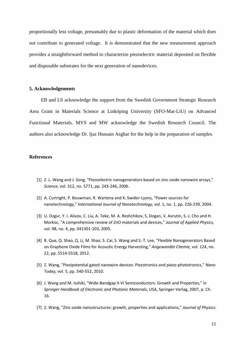
Figure 1 show typical SEM images of ZnO nanowires grown by the ACG method on
paper substrate. The ZnO NWs exhibit an apparent uniform distribution parallel to each other
and predominately in a perpendicular orientation to the substrate. The approximate diameter
of the NWs was about 150 ± 55 nm, while their length resulted 2300 ± 120 nm. The insets
show that the NWs have a hexagonal cross-section.
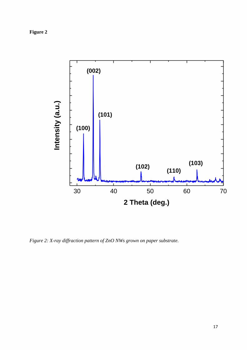
Figure 2 is a typical XRD pattern of ZnO NWs, revealing that all the diffraction peaks can be
indexed as the hexagonal wurtzite structured ZnO phase, consistent with the standard values
for bulk hexagonal ZnO [6, 25]. No diffraction peaks of Zn or other impurities have been
detected in the samples. The relatively enhanced intensity and sharp dominant peak at 34.40
degrees corresponding to the (002) peak indicates that the nanowires are highly c-axis
oriented and normal to the paper substrate surface [26]. The small peak between the (101) and
Page 8
7
(002) reflections can be related to a shift of the (002) peak probably due to stresses generated
in a folded part of the paper substrate.
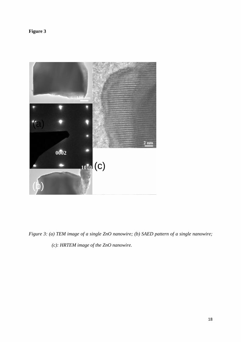
TEM analysis shows that the ZnO NWs have a single-crystalline structure and the axial
direction is along the [0001] as shown in Figure 3 (a). The corresponding selected area
electron diffraction (SAED) pattern in Figure 3(b) indicates that the ZnO NW has a single-
crystal hexagonal wurtzite structure. Figure 3(c) presents a high-resolution TEM image taken
from the top part of a ZnO NW. It can be clearly seen that the ZnO crystal lattices are well
oriented with the lattice spacing of 0.52 nm, which corresponds to the distance of (0001)
lattice planes, showing that the [0001] is the preferred growth direction for the ZnO NWs.
3.2 Converse Piezoelectric Effect
Converse piezoelectric tests were performed by nanoindentation testing using the
configuration shown in Figure 4. The converse piezoelectric effect is measured by applying a
DC voltage in the range 0 to -40 V while there is a low applied force to the sample of 50 µN,
enough to allow the tip to be always in physical contact with the ZnO nanowires. This
approach is similar to the method previously suggested by Rar et al for polycrystalline lead
zirconate titanate (PZT) and BaTiO3 piezoceramics [28], .ut in our case the applied voltage is
DC instead of AC.
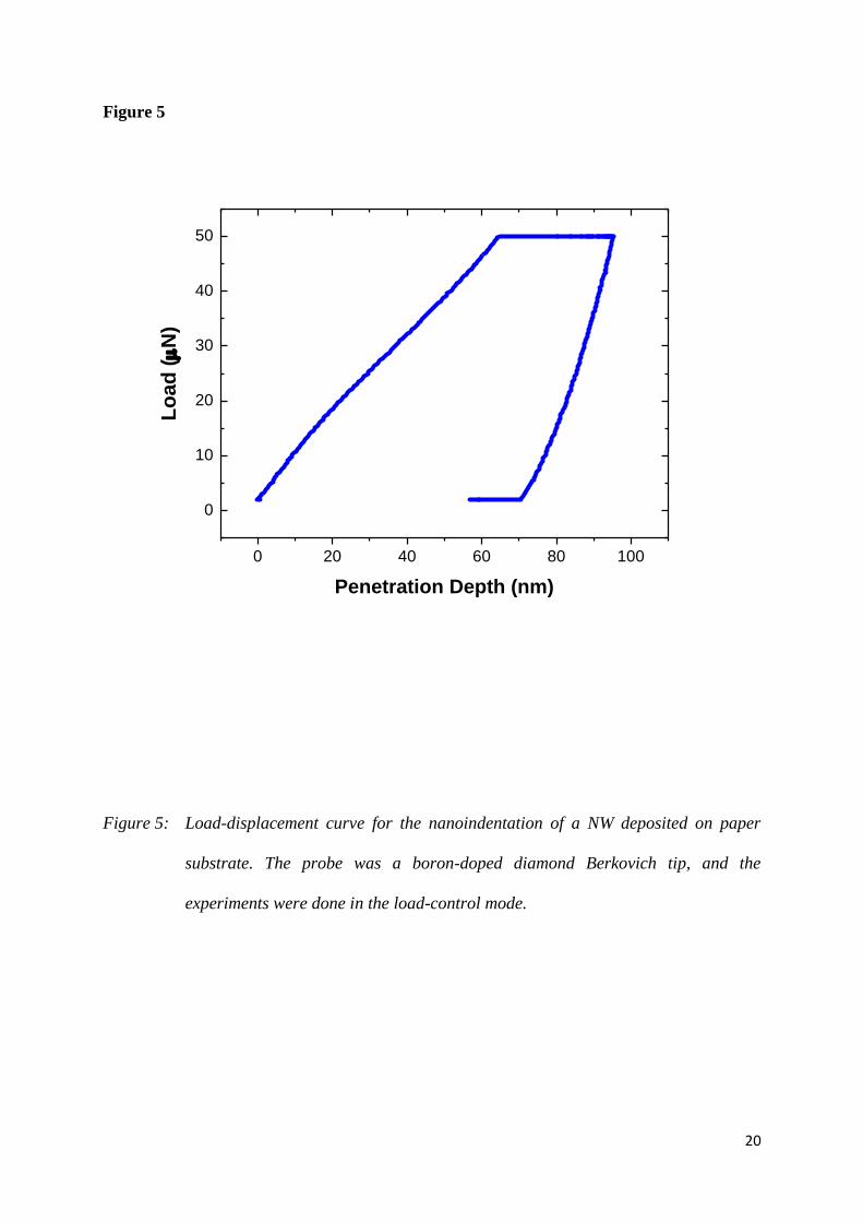
Figure 5 shows the load-displacement curve for the nanoindentation of NWs deposited
on paper substrate. It is possible to observe that with a maximum load of 50 µN, the NW
column is in stable equilibrium in the straight position, i.e., there is no buckling [29-30]. The
experiment also shows that, during the time that the nanoindenter applies the maximum force,
the curves present a creep of 35 nm. A similar creep behavior has been previously reported for
ZnO nanorods [24].
Page 9
8
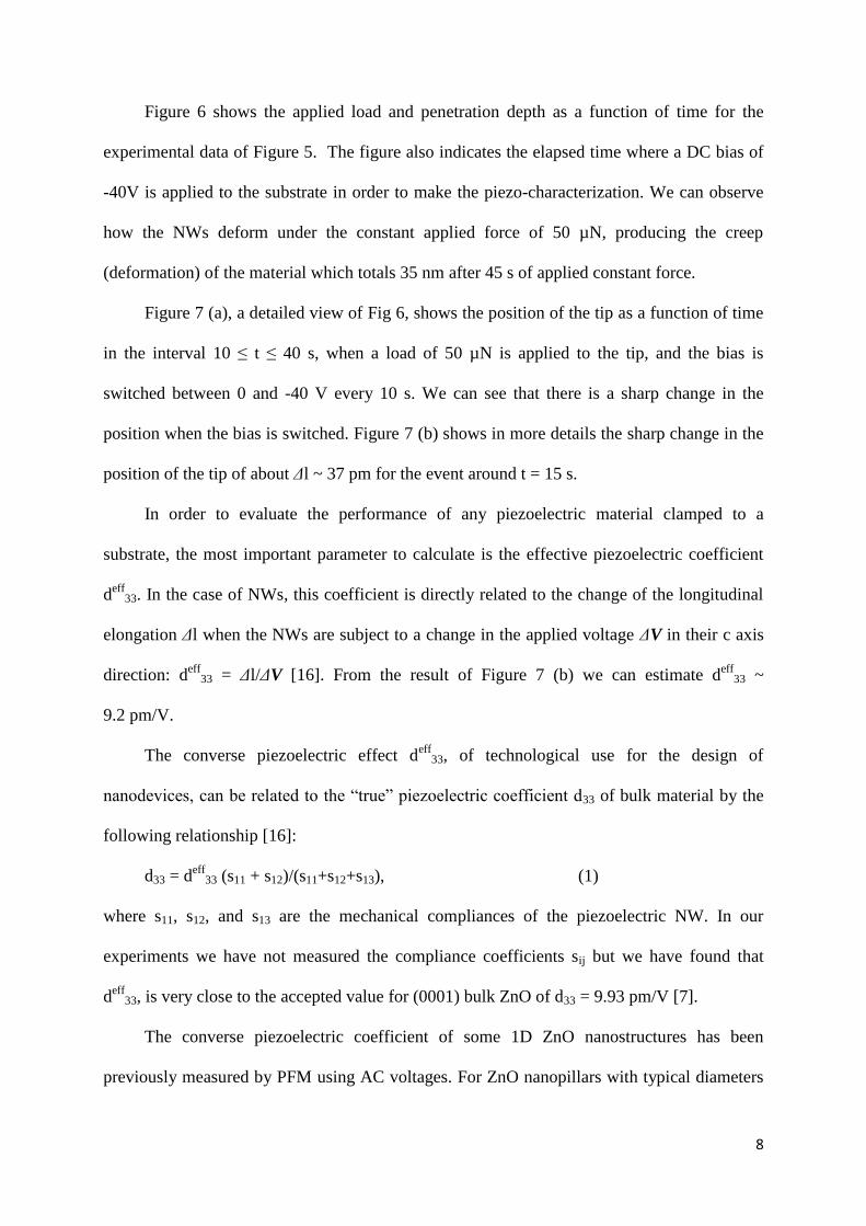
Figure 6 shows the applied load and penetration depth as a function of time for the
experimental data of Figure 5. The figure also indicates the elapsed time where a DC bias of
-40V is applied to the substrate in order to make the piezo-characterization. We can observe
how the NWs deform under the constant applied force of 50 µN, producing the creep
(deformation) of the material which totals 35 nm after 45 s of applied constant force.
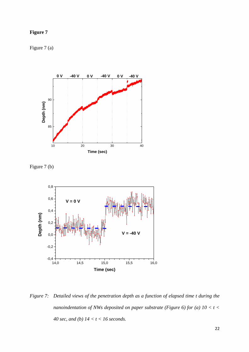
Figure 7 (a), a detailed view of Fig 6, shows the position of the tip as a function of time
in the interval 10 ≤ t ≤ 40 s, when a load of 50 µN is applied to the tip, and the bias is
switched between 0 and -40 V every 10 s. We can see that there is a sharp change in the
position when the bias is switched. Figure 7 (b) shows in more details the sharp change in the
position of the tip of about Δl ~ 37 pm for the event around t = 15 s.
In order to evaluate the performance of any piezoelectric material clamped to a
substrate, the most important parameter to calculate is the effective piezoelectric coefficient
deff
33. In the case of NWs, this coefficient is directly related to the change of the longitudinal
elongation Δl when the NWs are subject to a change in the applied voltage ΔV in their c axis
direction: deff
33 = Δl/ΔV [16]. From the result of Figure 7 (b) we can estimate deff
33 ~
9.2 pm/V.
The converse piezoelectric effect deff
33, of technological use for the design of
nanodevices, can be related to the “true” piezoelectric coefficient d33 of bulk material by the
following relationship [16]:
d33 = deff
33 (s11 + s12)/(s11+s12+s13), (1)
where s11, s12, and s13 are the mechanical compliances of the piezoelectric NW. In our
experiments we have not measured the compliance coefficients sij but we have found that
deff
33, is very close to the accepted value for (0001) bulk ZnO of d33 = 9.93 pm/V [7].
The converse piezoelectric coefficient of some 1D ZnO nanostructures has been
previously measured by PFM using AC voltages. For ZnO nanopillars with typical diameters
Page 10
9
of ~300 nm, a piezoelectric constant of deff
33 ~ 7.5 pm/V was obtained [31]. A similar study,
for ZnO NRs with diameters in the range 150-500 nm and length of 400-600 nm, reported a
variation of the piezoelectric constant from 0.4 to 9.5 pm/V [10]. The authors also observed
that the variation of the deff
33 was correlated to variations in the NRs resistivity: they
concluded that a high conductivity quenches the piezoelectric response. PFM was also used to
measure individual ZnO nanobelts in the (0001) surface, where d33 values in the range 3 to
26.7 pm/V were measured [20, 32]. To our knowledge, there is no data published about the
piezoelectric constant deff
33 of ZnO nanowires; the only reported values by PFM are generated
voltages presented in the context of piezoelectric nanogenerators ([1, 21] and references
therein).
3.4 Direct Piezoelectric Effect
Figure 8 shows the nanoindenter configuration used in our experiments. The direct
piezoelectric effect was obtained by performing nanoindentations under load control with
maximum load forces Fm ranging from 0.2 to 6 mN, while the generated piezoelectric voltage
was measured as a function of the applied loads. This approach is similar to the method
suggested by Koval et al for lead zirconate titanate thin films [1], but in their case the
collected data were transient currents generated during the indentation.
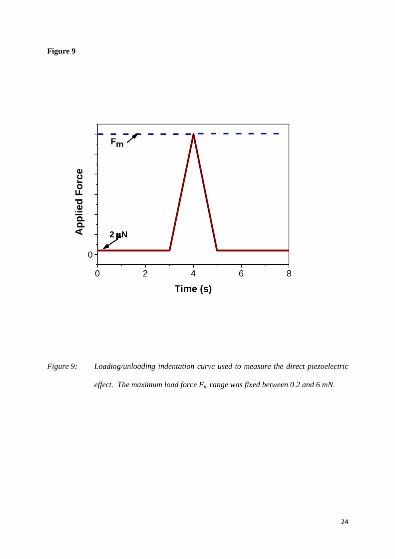
The loading/unloading indentation test consisted of an “impulse force” with four parts
(Figure 9): during the first 3 s the probe is in electric contact with the surface with an applied
load of 2 µN; then the force over the probe increases linearly in 1 s to the maximum value Fm;
in the third part the load decreases linearly in 1 s from Fm to 2 µN, and finally the probe rests
over the sample during 3 s with an applied load of 2 µN to allow possible relaxation processes
to occur. Ten indentations separated by a distance of ~50 µm were made in each sample.
Page 11
10
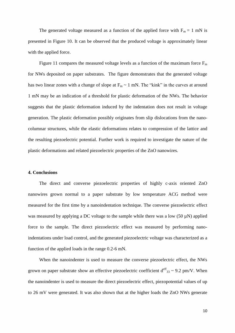
The generated voltage measured as a function of the applied force with Fm = 1 mN is
presented in Figure 10. It can be observed that the produced voltage is approximately linear
with the applied force.
Figure 11 compares the measured voltage levels as a function of the maximum force Fm
for NWs deposited on paper substrates. The figure demonstrates that the generated voltage
has two linear zones with a change of slope at Fm ~ 1 mN. The “kink” in the curves at around
1 mN may be an indication of a threshold for plastic deformation of the NWs. The behavior
suggests that the plastic deformation induced by the indentation does not result in voltage
generation. The plastic deformation possibly originates from slip dislocations from the nano-
columnar structures, while the elastic deformations relates to compression of the lattice and
the resulting piezoelectric potential. Further work is required to investigate the nature of the
plastic deformations and related piezoelectric properties of the ZnO nanowires.
4. Conclusions
The direct and converse piezoelectric properties of highly c-axis oriented ZnO
nanowires grown normal to a paper substrate by low temperature ACG method were
measured for the first time by a nanoindentation technique. The converse piezoelectric effect
was measured by applying a DC voltage to the sample while there was a low (50 µN) applied
force to the sample. The direct piezoelectric effect was measured by performing nano-
indentations under load control, and the generated piezoelectric voltage was characterized as a
function of the applied loads in the range 0.2-6 mN.
When the nanoindenter is used to measure the converse piezoelectric effect, the NWs
grown on paper substrate show an effective piezoelectric coefficient deff
33 ~ 9.2 pm/V. When
the nanoindenter is used to measure the direct piezoelectric effect, piezopotential values of up
to 26 mV were generated. It was also shown that at the higher loads the ZnO NWs generate
Page 12
11
proportionally less voltage, presumably due to plastic deformation of the material which does
not contribute to generated voltage. It is demonstrated that the new measurement approach
provides a straightforward method to characterize piezoelectric material deposited on flexible
and disposable substrates for the next generation of nanodevices.
5. Acknowledgements
EB and LS acknowledge the support from the Swedish Government Strategic Research
Area Grant in Materials Science at Linköping University (SFO-Mat-LiU) on Advanced
Functional Materials. MYS and MW acknowledge the Swedish Research Council. The
authors also acknowledge Dr. Ijaz Hussain Asghar for the help in the preparation of samples.
References
[1] Z. L. Wang and J. Song, "Piezoelectric nanogenerators based on zinc oxide nanowire arrays,"
Science, vol. 312, no. 5771, pp. 243-246, 2006.
[2] A. Curtright, P. Bouwman, R. Wartena and K. Swider-Lyons, "Power sources for
nanotechnology," International Journal of Nanotechnology, vol. 1, no. 1, pp. 226-239, 2004.
[3] U. Ozgur, Y. I. Alivov, C. Liu, A. Teke, M. A. Reshchikov, S. Dogan, V. Avrutin, S.-J. Cho and H.
Morkoc, "A comprehensive review of ZnO materials and devices," Journal of Applied Physics,
vol. 98, no. 4, pp. 041301-103, 2005.
[4] R. Que, Q. Shao, Q. Li, M. Shao, S. Cai, S. Wang and S.-T. Lee, "Flexible Nanogenerators Based
on Graphene Oxide Films for Acoustic Energy Harvesting," Angewandte Chemie, vol. 124, no.
22, pp. 5514-5518, 2012.
[5] Z. Wang, "Piezipotential gated nanowire devices: Piezotronics and piezo-phototronics," Nano
Today, vol. 5, pp. 540-552, 2010.
[6] J. Wang and M. Isshiki, "Wide-Bandgap II-VI Semiconductors: Growth and Properties," in
Springer Handbook of Electronic and Photonic Materials, USA, Springer-Verlag, 2007, p. Ch.
16.
[7] Z. Wang, "Zinc oxide nanostructures: growth, properties and applications," Journal of Physics:
Page 13
12
Condensed Matter, vol. 16, pp. R829-R858, 2004.
[8] C. Li, W. Guo, Y. Kong and H. Gao, "First-principles study of the dependence of ground-state
structural properties on the dimensionality and size of ZnO nanostructures," Physical Review
B, vol. 76, no. 3, p. 035322, 2007.
[9] S. Dai, M. Dunn and H. Park, "Piezoelectric constants for ZnO calculated using classical
polarizable core–shell potentials," Nanotechnology, vol. 21, no. 44, p. 445707, 2010.
[10] D. Scrymgeour and J. Hsu, "Correlated Piezoelectric and Electrical Properties in Individual
ZnO Nanorods," Nano Letters, vol. 8, no. 8, pp. 2204-2209, 2008.
[11]
Status and Future Prospects," Proceedings of the IEEE, vol. 98, no. 7, pp. 1255 - 1268, 2010.
[12] A. Wei, L. Pan and W. Huang, "Recent progress in the ZnO nanostructure-based sensors,"
Materials Science and Engineering B, vol. 176, no. 18, pp. 1409-1421, 2011.
[13] S. Arya, S. Saha, J. Ramirez-Vick, V. Gupta, S. Bhansali and S. Singh, "Recent advances in ZnO
nanostructures and thin films for biosensor applications: Review," Analytica Chimica Acta,
vol. 737, no. 8, pp. 1-21, 2012.
[14] S.-J. Chen, Y. Choe, L. Baumgartel, A. Lin and E. Kim, "Edge-released, piezoelectric MEMS
acoustic transducers in array configuration," Journal of Micromechanics and
Microengineering, vol. 222, p. 025005, 2012.
[15] M. Niederberger, "Nonaqueous Sol–Gel Routes to Metal Oxide Nanoparticles," Accounts of
Chemical Research, vol. 40, no. 9, p. 793–800, 2007.
[16] H. Espinosa, R. Bernal and M. Minary-Jolandan, "A Review of Mechanical and
Electromechanical Properties of Piezoelectric Nanowires," Advanced Materials, vol. 24, no.
34, p. 4656–4675, 2012.
[17] J. Zhou, Y. Gu, P. Fei, W. Mai, Y. Gao, R. Yang, G. Bao and Z. Wang, "Flexible Piezotronic Strain
Sensor," Nano Letters, vol. 8, no. 9, p. 3035–3040, 2008.
[18] H. Gullapalli, V. Vemuru, A. Kumar, A. Botello-Mendez, R. Vajtai, M. Terrones, S. Nagarajaiah
and P. Ajayan, "Flexible Piezoelectric ZnO–Paper Nanocomposite Strain Sensor," Small, vol. 6,
no. 15, p. 1641–1646, 2010.
[19] Y. Park, H. Choi, J.-H. Kim, J. Kim and Y.-B. Hahn, "High performance field-effect transistors
fabricated with laterally grown ZnO nanorods in solution," Nanotechnology, vol. 22, p.
185310, 2011.
[20] M.-H. Zhao, Z.-L. Wang and S.-X. Mao, "Piezoelectric Characterization of Individual Zinc Oxide
Nanobelt Probed by Piezoresponse Force Microscope," Nano Letters, vol. 4, no. 4, p. 587–
Page 14
13
590, 2004.
[21] M. Y. Soomro, I. Hussain, N. Bano, O. Nur and M. Willander, "Piezoelectric power generation
from zinc oxide nanowires grown on paper substrate," Physica Status Solidi (RRL) - Rapid
Research Letters, vol. 6, no. 2, pp. 80-82, 2012.
[22] A. Wadeasa, O. Nur and M. Willander, "The effect of the interlayer design on the
electroluminescence and electrical properties of n-ZnO nanorod/p-type blended polymer
hybrid light emitting diodes," Nanotechnology, vol. 20, p. 065710, 2009.
[23] X. X. Crispin, F. L. E. Jakobsson, A. Crispin, P. C. M. Grim, P. Andersson, A. Volodin, C. van
Haesendonck, M. Van der Auweraer, W. Salaneck and M. Berggren, "The Origin of the High
Conductivity of Poly(3,4- hy xy h h )−P y( y ) (PE T−PSS)
Plastic Electrodes," Chemistry of Materials, vol. 18, no. 8, p. 4354–4360, 2006.
[24] M. Soomro, I. Hussain, N. Bano, E. Broitman, .. O. Nur and M. Willander, "Nanoscale elastic
modulus of single horizontal ZnO nanorod using nanoindentation experiment," Nanoscale
Research Letters, vol. 7, p. 146, 2012.
[25] M. Soomro, I. Hussain, N. Bano, J. Lu, L. Hultman, .. O. Nur and M. Willander, "Growth,
Structural and Optical Characterization of ZnO Nanotubes on Disposable-Flexible Paper
Substrates by Low-Temperature Chemical Method," Journal of nanotechnology, p. 251863,
2012.
[26] M. Wang, C. Ye, Y. Zhang, H.-X. Wang, X.-Y. Zeng and L.-D. Zhang, "Seed-layer controlled
synthesis of well-aligned ZnO nanowire arrays via a low temperature aqueous solution
method," Journal of Materials Science: Materials in Electronics, vol. 19, no. 3, pp. 211-216,
2008.
[27] L. B. Freund and S. Suresh, Thin Film Materials, New York: Cambridge University Press, 2003.
[28] A. Rar, G. Pharr, W. Oliver, E. Karapetian and S. Kalinin, "Piezoelectric Nanoindentation,"
Journal of Materials Research, vol. 21, pp. 552-556, 2006.
[29] M. Riaz, O. Nur, M. Willander and P. Klason, "Buckling of ZnO nanowires under uniaxial
compression," Applied Physics Letters, vol. 92, no. 10, pp. 103118 - 103118-3, 2008.
[30] M. Riaz, A. Fulati, L. L. Yang, O. Nur, M. Willander and P. Klason, "Bending flexibility, kinking,
and buckling characterization of ZnO nanorods/nanowires grown on different substrates by
high and low temperature methods," Journal of Applied Physics, vol. 104, no. 10, pp. 104306
- 104306-8, 2008.
[31] H. Fan, W. Lee, R. Hauschild, M. Alexe, G. Le Rhun, R. Scholz, A. Dadgar, K. Nielsch, H. Kalt, A.
Krost, Z. M. and U. Gösele, "Template-Assisted Large-Scale Ordered Arrays of ZnO Pillars for
Optical and Piezoelectric Applications," Small, vol. 2, no. 4, pp. 561-568, 2006.
[32] M.-H. Zhao, "Nanomechanical and Electromechanical Characterization of Zinc Oxide
Page 15
14
Nanobelt Using Atomic Force Microscopy," PhD Thesis University of Pittsburgh, Pittsburgh,
2004.
[33] V. Koval, M. Reece and A. Bushby, "Ferroelectric/ferroelastic behavior and piezoelectric
response of lead zirconate titanate thin films under nanoindentation," Journal of Applied
Physics, vol. 97, p. 074301, 2005.
Legend to Figures
Figure 1: SEM image of ZnO nanowires grown on paper substrate. The inset shows a high
magnification image of a single ZnO nanowire with well-defined hexagonal end
planes
Figure 2: X-ray diffraction pattern of ZnO NWs grown on paper substrat.
Figure 3: (a) TEM image of a single ZnO nanowire; (b) SAED pattern of a single nanowire;
(c): HRTEM image of the ZnO nanowire.
Figure 4: Schematic drawing of the experimental setup for the measurement of the converse
piezoelectric effect by nanoindentation.
Figure 5: Load-displacement curve for the nanoindentation of a NW deposited on paper
substrate. The probe was a boron-doped diamond Berkovich tip, and the
experiments were done in the load-control mode.
Page 16
15
Figure 6: Applied load and penetration depth as a function of elapsed time during the
nanoindentation of ZnO NWs grown on paper substrate. The elapsed time where a
DC -40V bias is applied has been indicated as a center line.
Figure 7: Detailed views of the penetration depth as a function of elapsed time t during the
nanoindentation of NWs deposited on paper substrate (Figure 6) for (a) 10 < t <
40 sec, and (b) 14 < t < 16 seconds.
Figure 8: Schematic drawing of the experimental setup for the measurement of the direct
piezoelectric effect by nanoindentation.
Figure 9: Loading/unloading indentation curve used to measure the direct piezoelectric
effect. The maximum load force Fm range was fixed between 0.2 and 6 mN.
Figure 10: Applied load and corresponding generated piezoelectric voltage as a function
of the time for NWs grown on paper substrate. The maximum load force is 1
mN.
Figure 11: Generated piezo-voltage as a function of maximum applied load for NWs
grown on (a) paper substrate. The dotted lines are for guiding the eyes only.
Page 17
16
Figure 1
Figure 1: SEM image of ZnO nanowires grown on paper substrate. The inset shows a high
magnification image of a single ZnO nanowire with well-defined hexagonal end
planes
100 nm
0.5 µm
Page 18
17
Figure 2
30 40 50 60 70
(110)
In
ten
sit
y (
a.u
.)
2 Theta (deg.)
(100)
(002)
(101)
(102)(103)
Figure 2: X-ray diffraction pattern of ZnO NWs grown on paper substrate.
Page 19
18
Figure 3
Figure 3: (a) TEM image of a single ZnO nanowire; (b) SAED pattern of a single nanowire;
(c): HRTEM image of the ZnO nanowire.
0002
1010-
(a)
(c)
(b)
Page 20
19
Figure 4
Figure 4: Schematic drawing of the experimental setup for the measurement of the converse
piezoelectric effect by nanoindentation.
Page 21
20
Figure 5
0 20 40 60 80 100
0
10
20
30
40
50
L
oad
(N
)
Penetration Depth (nm)
Figure 5: Load-displacement curve for the nanoindentation of a NW deposited on paper
substrate. The probe was a boron-doped diamond Berkovich tip, and the
experiments were done in the load-control mode.
Page 22
21
Figure 6
0 10 20 30 40 50 60
0
20
40
60
80
100
120
140
160
180
200
0V0V0V 0V
-40V-40V
Time (sec)
De
pth
(n
m) -40V
-50
-40
-30
-20
-10
0
10
20
30
40
50
Lo
ad
(µ
N)
Figure 6: Applied load and penetration depth as a function of elapsed time during the
nanoindentation of ZnO NWs grown on paper substrate. The elapsed time where a
DC -40V bias is applied has been indicated as a center line.
Page 23
22
Figure 7
Figure 7 (a)
10 20 30 40
85
90
-40 V-40 V 0 V0 V-40 V
Dep
th (
nm
)
Time (sec)
0 V
Figure 7 (b)
14,0 14,5 15,0 15,5 16,0
-0,4
-0,2
0,0
0,2
0,4
0,6
0,8
V = -40 V
Dep
th (
nm
)
Time (sec)
V = 0 V
Figure 7: Detailed views of the penetration depth as a function of elapsed time t during the
nanoindentation of NWs deposited on paper substrate (Figure 6) for (a) 10 < t <
40 sec, and (b) 14 < t < 16 seconds.
Page 24
23
Figure 8
Figure 8: Schematic drawing of the experimental setup for the measurement of the direct
piezoelectric effect by nanoindentation.
Page 25
24
Figure 9
0 2 4 6 8
2 N
Ap
plied
Fo
rce
Time (s)
Fm
0
Figure 9: Loading/unloading indentation curve used to measure the direct piezoelectric
effect. The maximum load force Fm range was fixed between 0.2 and 6 mN.
Page 26
25
Figure 10
0 2 4 6 8
0
200
400
600
800
1000
Time (s)
Lo
ad
(µ
N)
0,000
0,004
0,008
0,012
Pie
zo
vo
lta
ge
(V
)
Figure 10: Applied load and corresponding generated piezoelectric voltage as a function
of the time for NWs grown on paper substrate. The maximum load force is 1
mN.
Page 27
26
Figure 11
0 1 2 3 4 5 6
0,00
0,01
0,02
0,03
Ge
ne
rate
d P
iezo
-vo
lta
ge
(V
)
Fm (mN)
Figure 11: Generated piezo-voltage as a function of maximum applied load for NWs
grown on (a) paper substrate. The dotted lines are for guiding the eyes only.