Nanoscale Probing of Thermal, Stress, and Optical Fields under Near-Field Laser Heating Xiaoduan Tang 1 , Shen Xu 1 , Xinwei Wang 1,2 * 1 Department of Mechanical Engineering, Iowa State University, Ames, Iowa, United States of America, 2 School of Environmental and Municipal Engineering, Qingdao Technological University, Qingdao, Shandong, P.R. China Abstract Micro/nanoparticle induced near-field laser ultra-focusing and heating has been widely used in laser-assisted nanopatterning and nanolithography to pattern nanoscale features on a large-area substrate. Knowledge of the temperature and stress in the nanoscale near-field heating region is critical for process control and optimization. At present, probing of the nanoscale temperature, stress, and optical fields remains a great challenge since the heating area is very small (,100 nm or less) and not immediately accessible for sensing. In this work, we report the first experimental study on nanoscale mapping of particle-induced thermal, stress, and optical fields by using a single laser for both near-field excitation and Raman probing. The mapping results based on Raman intensity variation, wavenumber shift, and linewidth broadening all give consistent conjugated thermal, stress, and near-field focusing effects at a 20 nm resolution (,l/26, l = 32 nm). Nanoscale mapping of near-field effects of particles from 1210 down to 160 nm demonstrates the strong capacity of such a technique. By developing a new strategy for physical analysis, we have de-conjugated the effects of temperature, stress, and near-field focusing from the Raman mapping. The temperature rise and stress in the nanoscale heating region is evaluated at different energy levels. High-fidelity electromagnetic and temperature field simulation is conducted to accurately interpret the experimental results. Citation: Tang X, Xu S, Wang X (2013) Nanoscale Probing of Thermal, Stress, and Optical Fields under Near-Field Laser Heating. PLoS ONE 8(3): e58030. doi:10.1371/journal.pone.0058030 Editor: Randen Lee Patterson, UC Davis School of Medicine, United States of America Received December 14, 2012; Accepted January 29, 2013; Published March 28, 2013 This is an open-access article, free of all copyright, and may be freely reproduced, distributed, transmitted, modified, built upon, or otherwise used by anyone for any lawful purpose. The work is made available under the Creative Commons CC0 public domain dedication. Funding: Financial support for this work was provided by the National Science Foundation (CMMI-0926704, CMMI-1200397, and CBET-0932573). The funders had no role in study design, data collection and analysis, decision to publish, or preparation of the manuscript. Competing Interests: The authors have declared that no competing interests exist. * E-mail: [email protected]Introduction The conventional optical microscope is diffraction-limited in imaging resolution to about half of the illuminating wavelengths. Some near-field techniques can help to improve the resolution, which is achieved by placing the detector very close to the object. Scanning tunneling microscopy (STM) and atomic force micros- copy (AFM), utilizing a tunneling current and force between the tip and the sample respectively, can image surfaces at the atomic level. With light probe, near-field scanning optical microscopy (NSOM) is capable of breaking the optical resolution limit by extensively employing the properties of evanescent waves [1,2]. However, NSOM has slow scanning speed and low imaging depth and the probe must be very close to the object. Taubner et al. improved subwavelength imaging of buried objects by using a silicon carbide superlens based near-field microscopy [3]. The superlens used a silver slab with periodic corrugations to enhance the evanescent waves of an object and convert them into propagating waves, so that the object could be imaged in the far-field [4]. The superlens was physically placed in the near-field of an object, however. An imaging technique called stochastic optical reconstruction microscopy (STORM) provided a high imaging resolution of approximately 20 nm by controlling the fluorescence emission from a single molecule, limited only by the number of photons emitted per switch cycle [5]. The above techniques are nearsighted, as the distance between the probe and object is in the near-field. Far-field superlenses (FSLs) capable of imaging beyond the diffraction limit in the far field have been developed [6–9]. Transparent microspheres or photonic metama- terials were used as FSLs to reach a resolution between l/3 and l/ 14. Nanoscale solid immersion lenses (nSILs) were developed for high-quality imaging which can resolve line objects at a resolution of l/2.2 [10]. However, it is hard to resolve a surface variation of objects below 50 nm with visible light. The technique employed in this work is capable of imaging a surface variation beyond the light diffraction limit in the far-field. The surface variation of an object in the horizontal plane is able to be distinguished at a resolution of l/26. Regarding nanoscale surface thermal and stress imaging, scanning thermal microscopy (SThM) has been reported as an established technique to measure nanoscale temperature distribu- tions by attaching a temperature sensor on the apex of a tiny tip. The imaging of phonon temperature distribution for electrically heated carbon nanotube circuits was reported with a spatial resolution of ,50 nm [11]. A near-field SThM (NSThM) operating in ultrahigh vacuum was developed to provide thermal imaging for a sample with a resolution of a few nanometers [12]. In thermometry, apertureless NSOM has been proposed by using an AFM tip or a nanoparticle. Temperature probing of silicon under AFM tip focused laser heating at a sub-10 nm scale was conducted via apertureless NSOM based on Raman thermometry [13]. Nanoscale thermal probing of graphene on 4H-SiC in the thickness direction was reported using Raman spectrometer with PLOS ONE | www.plosone.org 1 March 2013 | Volume 8 | Issue 3 | e58030
Transcript
Nanoscale Probing of Thermal, Stress, and Optical Fieldsunder Near-Field Laser HeatingXiaoduan Tang1, Shen Xu1, Xinwei Wang1,2*
1Department of Mechanical Engineering, Iowa State University, Ames, Iowa, United States of America, 2 School of Environmental and Municipal Engineering, Qingdao
Technological University, Qingdao, Shandong, P.R. China
Abstract
Micro/nanoparticle induced near-field laser ultra-focusing and heating has been widely used in laser-assistednanopatterning and nanolithography to pattern nanoscale features on a large-area substrate. Knowledge of thetemperature and stress in the nanoscale near-field heating region is critical for process control and optimization. At present,probing of the nanoscale temperature, stress, and optical fields remains a great challenge since the heating area is verysmall (,100 nm or less) and not immediately accessible for sensing. In this work, we report the first experimental study onnanoscale mapping of particle-induced thermal, stress, and optical fields by using a single laser for both near-field excitationand Raman probing. The mapping results based on Raman intensity variation, wavenumber shift, and linewidth broadeningall give consistent conjugated thermal, stress, and near-field focusing effects at a 20 nm resolution (,l/26, l= 32 nm).Nanoscale mapping of near-field effects of particles from 1210 down to 160 nm demonstrates the strong capacity of sucha technique. By developing a new strategy for physical analysis, we have de-conjugated the effects of temperature, stress,and near-field focusing from the Raman mapping. The temperature rise and stress in the nanoscale heating region isevaluated at different energy levels. High-fidelity electromagnetic and temperature field simulation is conducted toaccurately interpret the experimental results.
Citation: Tang X, Xu S, Wang X (2013) Nanoscale Probing of Thermal, Stress, and Optical Fields under Near-Field Laser Heating. PLoS ONE 8(3): e58030.doi:10.1371/journal.pone.0058030
Editor: Randen Lee Patterson, UC Davis School of Medicine, United States of America
Received December 14, 2012; Accepted January 29, 2013; Published March 28, 2013
This is an open-access article, free of all copyright, and may be freely reproduced, distributed, transmitted, modified, built upon, or otherwise used by anyone forany lawful purpose. The work is made available under the Creative Commons CC0 public domain dedication.
Funding: Financial support for this work was provided by the National Science Foundation (CMMI-0926704, CMMI-1200397, and CBET-0932573). The funders hadno role in study design, data collection and analysis, decision to publish, or preparation of the manuscript.
Competing Interests: The authors have declared that no competing interests exist.
The conventional optical microscope is diffraction-limited in
imaging resolution to about half of the illuminating wavelengths.
Some near-field techniques can help to improve the resolution,
which is achieved by placing the detector very close to the object.
Scanning tunneling microscopy (STM) and atomic force micros-
copy (AFM), utilizing a tunneling current and force between the
tip and the sample respectively, can image surfaces at the atomic
level. With light probe, near-field scanning optical microscopy
(NSOM) is capable of breaking the optical resolution limit by
extensively employing the properties of evanescent waves [1,2].
However, NSOM has slow scanning speed and low imaging depth
and the probe must be very close to the object. Taubner et al.
improved subwavelength imaging of buried objects by using
a silicon carbide superlens based near-field microscopy [3]. The
superlens used a silver slab with periodic corrugations to enhance
the evanescent waves of an object and convert them into
propagating waves, so that the object could be imaged in the
far-field [4]. The superlens was physically placed in the near-field
of an object, however. An imaging technique called stochastic
optical reconstruction microscopy (STORM) provided a high
imaging resolution of approximately 20 nm by controlling the
fluorescence emission from a single molecule, limited only by the
number of photons emitted per switch cycle [5]. The above
techniques are nearsighted, as the distance between the probe and
object is in the near-field. Far-field superlenses (FSLs) capable of
imaging beyond the diffraction limit in the far field have been
developed [6–9]. Transparent microspheres or photonic metama-
terials were used as FSLs to reach a resolution between l/3 and l/14. Nanoscale solid immersion lenses (nSILs) were developed for
high-quality imaging which can resolve line objects at a resolution
of l/2.2 [10]. However, it is hard to resolve a surface variation of
objects below 50 nm with visible light. The technique employed in
this work is capable of imaging a surface variation beyond the light
diffraction limit in the far-field. The surface variation of an object
in the horizontal plane is able to be distinguished at a resolution of
l/26.Regarding nanoscale surface thermal and stress imaging,
scanning thermal microscopy (SThM) has been reported as an
established technique to measure nanoscale temperature distribu-
tions by attaching a temperature sensor on the apex of a tiny tip.
The imaging of phonon temperature distribution for electrically
heated carbon nanotube circuits was reported with a spatial
resolution of ,50 nm [11]. A near-field SThM (NSThM)
operating in ultrahigh vacuum was developed to provide thermal
imaging for a sample with a resolution of a few nanometers [12].
In thermometry, apertureless NSOM has been proposed by using
an AFM tip or a nanoparticle. Temperature probing of silicon
under AFM tip focused laser heating at a sub-10 nm scale was
conducted via apertureless NSOM based on Raman thermometry
[13]. Nanoscale thermal probing of graphene on 4H-SiC in the
thickness direction was reported using Raman spectrometer with
PLOS ONE | www.plosone.org 1 March 2013 | Volume 8 | Issue 3 | e58030
a resolution down to 1 nm [14]. Temperature and stress surface
mapping in a doped polysilicon microheater and a silicon
microcantilever has been reported at microscale using Raman
spectroscopy [15]. Recently, Reserbat-Plantey et al. developed
a non-invasive optical probe to provide stress mapping at
nanoscale within a nanoelectromechanical system by combining
Raman spectroscopy with Fizeau interferometry [16]. As Raman
spectroscopy is a unique far-field technique sensitive to both
temperature and stress fields [15,17], in this paper, we use it to
achieve thermal and stress surface mapping at nanoscale.
Monolayer of micro/nanoparticles is attractive due to the
generation of surface textures [18]. Laser-assisted nanopatterning
and nanoimprinting lithography has been proved to be able to
pattern nanoscale features on a large-area substrate [19–21]. Pit
arrays have been created on metallic surfaces under particle-
enhanced laser irradiation [22]. Due to the wide application of
particles, theoretical studies about optical field enhancement by
micro/nano particles have been reported. Analytical calculation of
a dielectric sphere under laser illumination has been performed by
using the Mie scattering theory [23]. Optical field distributions of
a particle on a substrate under normally irradiated laser were
obtained [20,22,24]. Moreover, simulation of laser interaction
with materials (SLIM) was used to theoretically calculate the
temperature of a substrate beneath particles with laser irradiation
[22,25]. Nanoscale experimental imaging using microparticles is
rarely reported. McLeod and Arnold employed a microsphere as
an objective lens for nanopatterning by focusing a laser beam on
a substrate [20]. Arbitrary patterns and individual features were
generated with a minimum size of 100 nm and a positioning
accuracy less than 40 nm. Wang et al. employed ordinary
transparent microspheres to collect near-field object information
and formed virtual images at a 50 nm resolution [6]. Light
intensity distributions for solid immersion lens, a sphere and
a particle on substrates were calculated and compared. In laser-
assisted surface patterning using micro/nanoparticles, very high
temperature rise and local stress will be induced and needed to
induce surface structure change. Knowledge of the temperature
and stress information in the near-field heating region under
micro/nanoparticles is critical for process control and optimiza-
tion. In our previous work, the temperature field inside silicon
under particle induced laser heating has been measured at
a subwavelength resolution [26]. To our knowledge, however,
no experiment about structure imaging with temperature and
stress information inside a substrate-particle system using a far-
field method has been reported. Such measurement is very
challenging since the near-field heating area in the substrate is very
small, usually around 100 nm or smaller. Also this area is
immediately below the particle, so retrieving the thermal and
stress information of this region is very difficult.
In this work, far-field nanoscale mapping of conjugated thermal,
stress, and near-field focusing effects in a silicon substrate beneath
silica particles under laser irradiation is conducted for the first time
using Raman spectroscopy at a 20 nm lateral resolution (, l/26).Methodologies are developed to separate the optical, thermal, and
stress effects and evaluate the temperature rise and local stress in
particle-induced near-field focusing. The electromagnetic and
temperature fields inside the substrate-particle system are simu-
lated to interpret the measurement results. Our experimental work
on nanoscale imaging has great potential in molecular imaging,
nanolithography, nanotexturing and biomedical sensing.
Experimental Details
Sample PreparationSilica particles are patterned on silicon wafers in a monolayer
using a tilting technique [27]. Surfactant (triton-X: methanol
= 1:400 by volume) is mixed with monodisperse silica particle
suspensions [28]. The suspensions have silica particles with a solid
percentage of 10% suspended in water. As-received silica spheres
of 200 nm (Corpuscular), 400 nm (Polysciences), 800 nm, and
1210 nm (Bangs Laboratories) diameters are used without any
surface treatment. Silicon (100) wafers (University Wafer) are
cleaned in acetone and then deionized water for an hour with
ultrasonic agitation. These wafers are placed on glass slides, which
are tilted on a table with an angle of about 10u [27]. The mixture
is dispensed onto substrates using a syringe and left to dry for
about a half hour in the air. Then a 2-D monolayer of particles is
formed on the substrate. Large areas of monolayer particles can be
identified under a scanning electron microscope (SEM, FEI
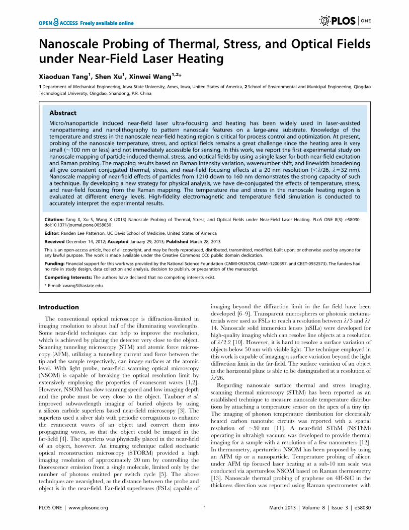
Quanta 250). Figure 1 shows typical SEM images of a silica
monolayer of 1210 nm diameter assembled on silicon wafers. The
compact assembled area can extend over a large area, up to
1 mm2, which is much larger than the laser spot area used in our
experiments (,0.5 mm2). The average diameter of the particles
shown in Fig. 1(b) is about 1120 nm, a little smaller than the
nominal diameter reported by the company.
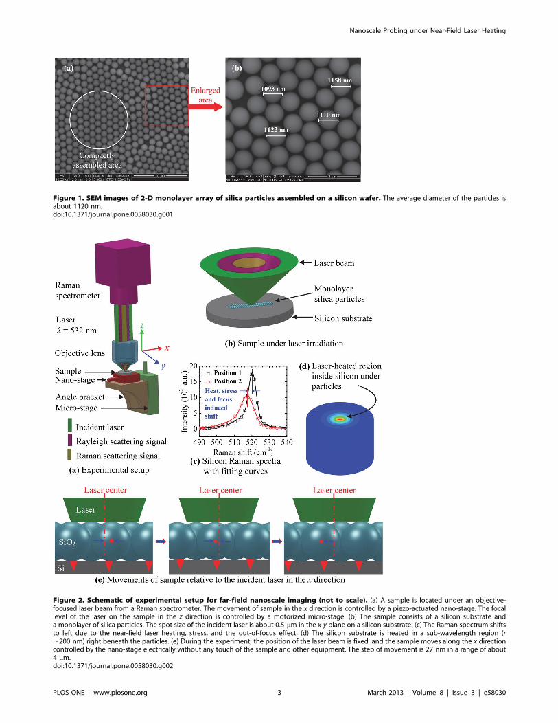
Nanoscale MappingFigure 2 shows schematic of the experimental setup for the
nanoscale structural imaging. The Raman scattering system
consists of a confocal Raman spectrometer (VoyageTM, B&W
Tek) and a microscope (Olympus BX51). Raman spectra are taken
at room temperature by using a 532 nm laser line at variable
power from 1.2–4.7 mW. The laser beam is focused by a 1006objective lens (NA =0.80). The movements of the sample are
controlled by a piezo-actuated nano-stage (ThorLabs NFL5DP20)
in the x direction (imaging direction) and a motorized translation
stage (ThorLabs MT1-Z8) in the z direction. These two stages are
vertically assembled together. The piezo-actuated range of the
nano-stage is 20 mm with a resolution of 20 nm. The sample
position in the z direction is adjusted by the motorized stage to
change the focal level of the incident laser within a range of
12 mm and a location accuracy of 0.1 mm. The incident laser used
as both Raman probing and heating source is focused on the silica
particles by the objective lens. The laser is found uniformly
distributed in space, and the spot size of the laser is about 500 nm,
determined by using a blade method. Due to the effect of the
particles, the laser beam is further focused on the silicon substrate
under the particles and heats up the substrate. The size of the
near-field focused area is about 200 nm. The excited Raman
scattering signals and Rayleigh scattering signals are collected by
using the same objective. Raman spectra of silicon substrate with
silica particles on the top at different positions in the x direction are
obtained and fitted using the Gaussian function.
The near-field heating and thermal stress inside the silicon
substrate is affected by factors including the particle diameter,
energy flux and focal level of the laser. The particle diameter and
laser energy flux can be determined precisely before the
experiments. In the experiments, it is critical to pay attention to
the laser focal level in order to obtain high accuracy and
repeatability of Raman signals. The position of the sample is
adjusted near the focal plane within a distance of about 6 mm.
Raman spectra are obtained at each level and the background
noise is subtracted to obtain sound Raman signals. Raman
intensity, wavenumber, and linewidth (full width at half maximum)
Nanoscale Probing under Near-Field Laser Heating
PLOS ONE | www.plosone.org 2 March 2013 | Volume 8 | Issue 3 | e58030
Figure 1. SEM images of 2-D monolayer array of silica particles assembled on a silicon wafer. The average diameter of the particles isabout 1120 nm.doi:10.1371/journal.pone.0058030.g001
Figure 2. Schematic of experimental setup for far-field nanoscale imaging (not to scale). (a) A sample is located under an objective-focused laser beam from a Raman spectrometer. The movement of sample in the x direction is controlled by a piezo-actuated nano-stage. The focallevel of the laser on the sample in the z direction is controlled by a motorized micro-stage. (b) The sample consists of a silicon substrate anda monolayer of silica particles. The spot size of the incident laser is about 0.5 mm in the x-y plane on a silicon substrate. (c) The Raman spectrum shiftsto left due to the near-field laser heating, stress, and the out-of-focus effect. (d) The silicon substrate is heated in a sub-wavelength region (r,200 nm) right beneath the particles. (e) During the experiment, the position of the laser beam is fixed, and the sample moves along the x directioncontrolled by the nano-stage electrically without any touch of the sample and other equipment. The step of movement is 27 nm in a range of about4 mm.doi:10.1371/journal.pone.0058030.g002
Nanoscale Probing under Near-Field Laser Heating
PLOS ONE | www.plosone.org 3 March 2013 | Volume 8 | Issue 3 | e58030
are affected by the focal level when other environmental factors
are fixed. Raman intensity and wavenumber decrease, and
linewidth broadens when the sample moves away from the focal
plane in the z direction [26].
A group of Raman spectra are obtained in the z direction before
imaging in order to determine the focal level. The focal level is
selected with the highest Raman intensity in the group. The
sample is then fixed to the focal level without any vertical shift.
Environmental factors such as the change of room temperature
and movement of the objective would lead to a Raman spectrum
difference. Therefore, the imaging process is followed immediately
to minimize the effect of environmental factors. The sample is
scanned along the x direction in a maximum range of 4.0 mm with
a step of 27 or 53 nm. The movement is controlled electrically
without any touch of the sample, stage, Raman spectrometer,
microscope and other related equipment that would affect the
quality of Raman signals. The Raman spectra change with the
nanoscale movement of the sample is finally obtained. The highest
energy flux is first used in the experiment, following by 79%, 50%,
and 25% of the maximum energy.
De-Conjugation of Thermal, Stress, and Optical FieldsIn order to investigate the temperature rise and thermal stress
caused by particle near-field focusing, experiments on silicon with
particles on the surface and bare silicon are both conducted. The
incident laser is first focused on the particles of the sample. The
Raman spectra for silicon under monolayer silica particles are
taken under four energy fluxes. Bare silicon is located around the
particles in the margin of the sample. Without any movement of
Raman spectrometer, the margin of the sample is moved to the
laser center to obtain the Raman spectra for bare silicon. The laser
is then adjusted to focus on the silicon and four energy fluxes are
used as well. The integration time and measurement average are
the same for those for silicon with particles. A group data of
Raman spectra at different focal levels around the focal plane are
obtained for each case. The Raman spectrum with the highest
intensity is selected to represent each result. By using this method,
the differences between the environmental situations for both bare
silicon and silicon with particles are suppressed to the minimal
level.
Results and Discussion
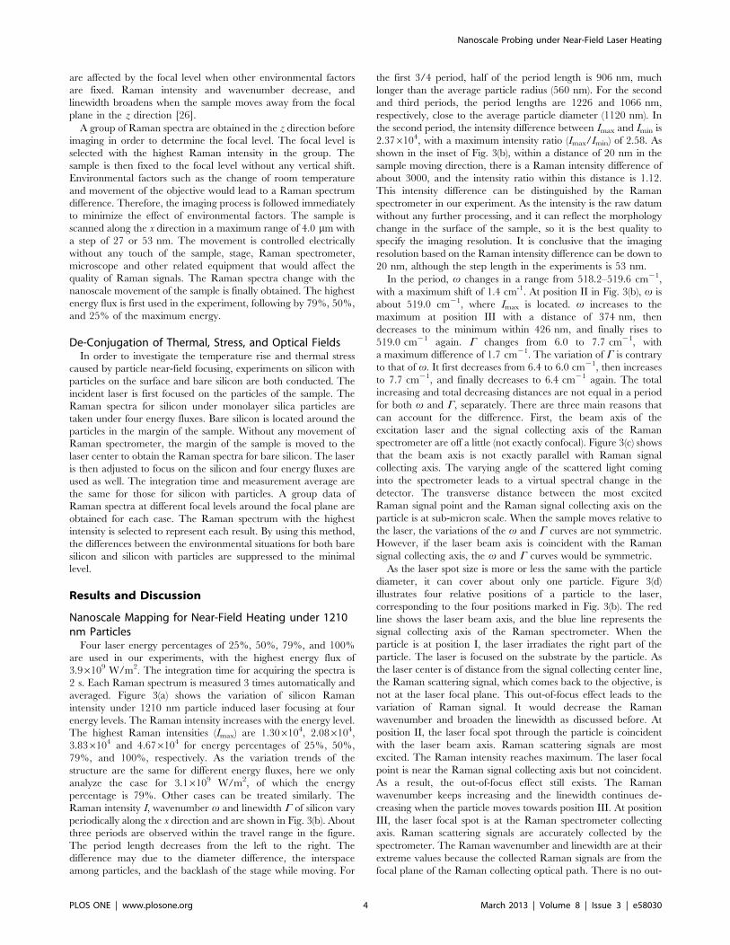
Nanoscale Mapping for Near-Field Heating under 1210nm ParticlesFour laser energy percentages of 25%, 50%, 79%, and 100%
are used in our experiments, with the highest energy flux of
3.96109 W/m2. The integration time for acquiring the spectra is
2 s. Each Raman spectrum is measured 3 times automatically and
averaged. Figure 3(a) shows the variation of silicon Raman
intensity under 1210 nm particle induced laser focusing at four
energy levels. The Raman intensity increases with the energy level.
The highest Raman intensities (Imax) are 1.306104, 2.086104,
3.836104 and 4.676104 for energy percentages of 25%, 50%,
79%, and 100%, respectively. As the variation trends of the
structure are the same for different energy fluxes, here we only
analyze the case for 3.16109 W/m2, of which the energy
percentage is 79%. Other cases can be treated similarly. The
Raman intensity I, wavenumber v and linewidth C of silicon vary
periodically along the x direction and are shown in Fig. 3(b). About
three periods are observed within the travel range in the figure.
The period length decreases from the left to the right. The
difference may due to the diameter difference, the interspace
among particles, and the backlash of the stage while moving. For
the first 3/4 period, half of the period length is 906 nm, much
longer than the average particle radius (560 nm). For the second
and third periods, the period lengths are 1226 and 1066 nm,
respectively, close to the average particle diameter (1120 nm). In
the second period, the intensity difference between Imax and Imin is
2.376104, with a maximum intensity ratio (Imax/Imin) of 2.58. As
shown in the inset of Fig. 3(b), within a distance of 20 nm in the
sample moving direction, there is a Raman intensity difference of
about 3000, and the intensity ratio within this distance is 1.12.
This intensity difference can be distinguished by the Raman
spectrometer in our experiment. As the intensity is the raw datum
without any further processing, and it can reflect the morphology
change in the surface of the sample, so it is the best quality to
specify the imaging resolution. It is conclusive that the imaging
resolution based on the Raman intensity difference can be down to
20 nm, although the step length in the experiments is 53 nm.
In the period, v changes in a range from 518.2–519.6 cm21,
with a maximum shift of 1.4 cm-1. At position II in Fig. 3(b), v is
about 519.0 cm21, where Imax is located. v increases to the
maximum at position III with a distance of 374 nm, then
decreases to the minimum within 426 nm, and finally rises to
519.0 cm21 again. C changes from 6.0 to 7.7 cm21, with
a maximum difference of 1.7 cm21. The variation of C is contrary
to that of v. It first decreases from 6.4 to 6.0 cm21, then increases
to 7.7 cm21, and finally decreases to 6.4 cm21 again. The total
increasing and total decreasing distances are not equal in a period
for both v and C, separately. There are three main reasons that
can account for the difference. First, the beam axis of the
excitation laser and the signal collecting axis of the Raman
spectrometer are off a little (not exactly confocal). Figure 3(c) shows
that the beam axis is not exactly parallel with Raman signal
collecting axis. The varying angle of the scattered light coming
into the spectrometer leads to a virtual spectral change in the
detector. The transverse distance between the most excited
Raman signal point and the Raman signal collecting axis on the
particle is at sub-micron scale. When the sample moves relative to
the laser, the variations of the v and C curves are not symmetric.
However, if the laser beam axis is coincident with the Raman
signal collecting axis, the v and C curves would be symmetric.
As the laser spot size is more or less the same with the particle
diameter, it can cover about only one particle. Figure 3(d)
illustrates four relative positions of a particle to the laser,
corresponding to the four positions marked in Fig. 3(b). The red
line shows the laser beam axis, and the blue line represents the
signal collecting axis of the Raman spectrometer. When the
particle is at position I, the laser irradiates the right part of the
particle. The laser is focused on the substrate by the particle. As
the laser center is of distance from the signal collecting center line,
the Raman scattering signal, which comes back to the objective, is
not at the laser focal plane. This out-of-focus effect leads to the
variation of Raman signal. It would decrease the Raman
wavenumber and broaden the linewidth as discussed before. At
position II, the laser focal spot through the particle is coincident
with the laser beam axis. Raman scattering signals are most
excited. The Raman intensity reaches maximum. The laser focal
point is near the Raman signal collecting axis but not coincident.
As a result, the out-of-focus effect still exists. The Raman
wavenumber keeps increasing and the linewidth continues de-
creasing when the particle moves towards position III. At position
III, the laser focal spot is at the Raman spectrometer collecting
axis. Raman scattering signals are accurately collected by the
spectrometer. The Raman wavenumber and linewidth are at their
extreme values because the collected Raman signals are from the
focal plane of the Raman collecting optical path. There is no out-
Nanoscale Probing under Near-Field Laser Heating
PLOS ONE | www.plosone.org 4 March 2013 | Volume 8 | Issue 3 | e58030
of-focus effect at position III. The Raman intensity is not quite
high because part of the particle is outside of the laser beam. From
position III to IV, the collected Raman signals become more out of
focus. Thus, the Raman wavenumber goes down and linewidth
broadens. In addition, the laser is focused only by part of the
particle, so the Raman intensity is becoming weaker. Based on this
analysis and the distance between the intensity peak and
wavenumber peak [Fig. 3(b)] we conclude that the laser beam
axis and the Raman signal collecting axis is off by about 374 nm
under the 1210 nm particle near-field focusing. As the two axes
are not exactly parallel, while the particle size varies, the distance
between the two axes on the particle would be different. Under
400 nm silica particle focusing, the distance between these two
focal centers becomes smaller, around 159 nm.
The second reason is that part of the Raman signals come from
the silicon wafer under the spacing among particles. As the laser
beam is pre-focused on the particles by the objective lens, the focal
level for the silicon beneath the particles is at a higher position
than the focal plane. This affects the Raman wavenumber and
linewidth of silicon. The third reason may be due to the beam
deflection caused by thermal expansion. The local silicon under
the particle center is heated by the laser beam and expands. The
heated silicon surface is no longer perpendicular to the propaga-
tion direction of the laser, which causes beam deflection. The
beam deflection affects the Raman signal of silicon.
De-Conjugation of Thermal, Stress, and Optical EffectsFor the nanoscale imaging (Fig. 3) based on the Raman
intensity, wavenumber, and linewidth, their variation against
location reflects a combined effect of near-field optical heating,
local stress, and optical field variation in space. Physically, it is
possible to de-conjugate these three effects and obtain quantitative
information about the nanoscale local stress and temperature. To
do this, the Raman spectra for silicon under monolayer silica
particles and for bare silicon are compared under four energy
fluxes, respectively. The highest energy flux is 3.96109 W/m2, and
the four energy percentages are 25%, 50%, 79%, and 100%. The
integration time is 2 s. The Raman spectra at various sample
positions and focal levels are obtained, and position II, as shown in
Fig. 3, is selected to determine the thermal response of silicon. At
this position, Raman intensity reaches its maximum value.
First of all, by studying the Raman intensity variation against
laser energy, the temperature rise under near-field heating is
evaluated. The Raman intensity for silicon under silica particles
(ISiO2) and that for bare silicon (ISi) are shown in Fig. 4(a). ISiO2
is
higher than ISi for each energy percentage because of the particle
focusing. The intensity ratio ISiO2=ISi decreases linearly with the
laser energy. Based on this ratio change against energy,
extrapolation is conducted to determine the ratio at zero laser
energy ISiO2=ISi½ �E~0. The normalized intensity ratio
ISiO2=ISi½ �= ISiO2
=ISi½ �E~0 decreases with laser energy. From the
Figure 3. Nanoscale mapping for near-field heating under 1210 nm particles. (a) Raman intensity I variation for silicon along the mappingdirection under particles of 1210 nm diameter with laser irradiation. (b) The x direction variation of Raman intensity I, Raman wavenumber v, andlinewidth C for silicon with laser irradiation of 3.16109 W/m2 (79%). (c) The distance between laser beam axis and Raman signal collecting axis ofRaman spectrometer. (d) The position of a silica particle relative to the laser beam axis and Raman signal collecting axis to explain the observedRaman variation in space.doi:10.1371/journal.pone.0058030.g003
Nanoscale Probing under Near-Field Laser Heating
PLOS ONE | www.plosone.org 5 March 2013 | Volume 8 | Issue 3 | e58030
decreasing trend, the temperature rise information can be
extracted. The physics is as follows. There are three main factors
that would affect the Raman intensity. Thus the Raman intensity
can be expressed as I~f1f2f3(DT) where f1 denotes the intensity
change due to the system alignment; f2 represents the intensity
change caused by the laser energy effect, which is proportional to
the laser energy; and f3(DT) is the intensity variation induced by
the temperature rise. For silicon with silica particles on its top, we
have ISiO2~f1f2f3(DT). But for bare silicon, Isi = f1f2, as the
temperature rise is negligible here because of the large thermal
conductivity of silicon. Isi is acquired immediately after ISiO2, so f1
and f2 are the same for both ISiO2and Isi separately. Thus, the
intensity ratio is only relative to temperature rise:
ISiO2=ISi~f3(DT). The Raman intensity of silicon reduces with
the increase of temperature. This is because high temperature,
which is caused by particle induced heating, changes the band
structure in silicon, and it restricts the photon interactions
necessary to generate Raman signals. The state density and
energy of phonons increase as temperature rises, leading to
a reduction of Raman intensity. In order to determine the thermal
response inside silicon under laser irradiation, the temperature
dependence of Raman intensity is needed. In our calibration,
shown in the inset of Fig. 4(b), the normalized intensity I/I0 for
bare silicon decreases with temperature, where I0 is the intensity of
silicon at 292.0 K. The integration time is 2 s, and the laser energy
is 8.66108 W/m2. The attained linear fitting slope for normalized
Raman intensity against temperature is 20.00249 K21 at
temperatures from 290 to 440 K. Figure 4(b) shows that the
normalized intensity ratio ISiO2=ISi½ �= ISiO2
=ISi½ �E~0 reduces when
energy flux increases. Based on the relation between intensity and
temperature, the temperature rise inside silicon due to particle
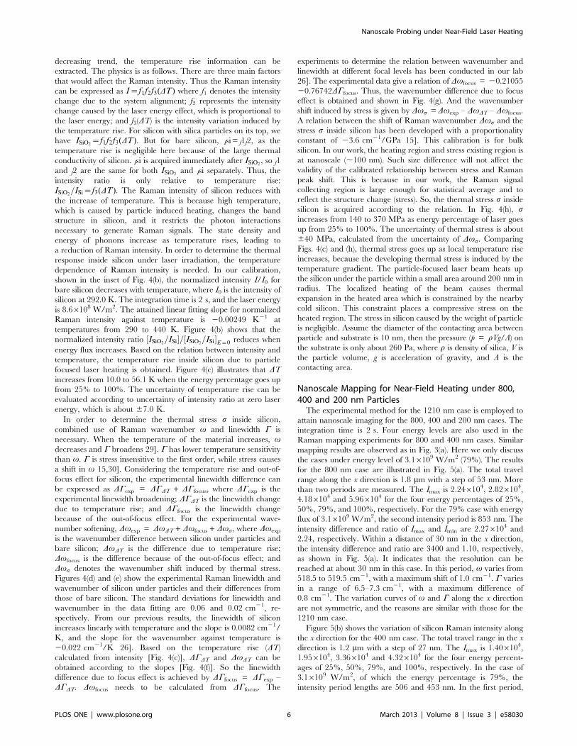
focused laser heating is obtained. Figure 4(c) illustrates that DTincreases from 10.0 to 56.1 K when the energy percentage goes up
from 25% to 100%. The uncertainty of temperature rise can be
evaluated according to uncertainty of intensity ratio at zero laser
energy, which is about 67.0 K.
In order to determine the thermal stress s inside silicon,
combined use of Raman wavenumber v and linewidth C is
necessary. When the temperature of the material increases, vdecreases and C broadens 29]. C has lower temperature sensitivity
than v. C is stress insensitive to the first order, while stress causes
a shift in v 15,30]. Considering the temperature rise and out-of-
focus effect for silicon, the experimental linewidth difference can
be expressed as DCexp = DCDT + DCfocus, where DCexp is the
experimental linewidth broadening; DCDT is the linewidth change
due to temperature rise; and DCfocus is the linewidth change
because of the out-of-focus effect. For the experimental wave-
number softening, Dvexp = DvDT + Dvfocus + Dvs, where Dvexp
is the wavenumber difference between silicon under particles and
bare silicon; DvDT is the difference due to temperature rise;
Dvfocus is the difference because of the out-of-focus effect; and
Dvs denotes the wavenumber shift induced by thermal stress.
Figures 4(d) and (e) show the experimental Raman linewidth and
wavenumber of silicon under particles and their differences from
those of bare silicon. The standard deviations for linewidth and
wavenumber in the data fitting are 0.06 and 0.02 cm21, re-
spectively. From our previous results, the linewidth of silicon
increases linearly with temperature and the slope is 0.0082 cm21/
K, and the slope for the wavenumber against temperature is
20.022 cm21/K 26]. Based on the temperature rise (DT)calculated from intensity [Fig. 4(c)], DCDT and DvDT can be
obtained according to the slopes [Fig. 4(f)]. So the linewidth
difference due to focus effect is achieved by DCfocus = DCexp –
DCDT. Dvfocus needs to be calculated from DCfocus. The
experiments to determine the relation between wavenumber and
linewidth at different focal levels has been conducted in our lab
26]. The experimental data give a relation of Dvfocus = 20.21055
20.76742DCfocus. Thus, the wavenumber difference due to focus
effect is obtained and shown in Fig. 4(g). And the wavenumber
shift induced by stress is given by Dvs =Dvexp – DvDT – Dvfocus.
A relation between the shift of Raman wavenumber Dvs and the
stress s inside silicon has been developed with a proportionality
constant of 23.6 cm21/GPa 15]. This calibration is for bulk
silicon. In our work, the heating region and stress existing region is
at nanoscale (,100 nm). Such size difference will not affect the
validity of the calibrated relationship between stress and Raman
peak shift. This is because in our work, the Raman signal
collecting region is large enough for statistical average and to
reflect the structure change (stress). So, the thermal stress s inside
silicon is acquired according to the relation. In Fig. 4(h), sincreases from 140 to 370 MPa as energy percentage of laser goes
up from 25% to 100%. The uncertainty of thermal stress is about
640 MPa, calculated from the uncertainty of Dvs. Comparing
Figs. 4(c) and (h), thermal stress goes up as local temperature rise
increases, because the developing thermal stress is induced by the
temperature gradient. The particle-focused laser beam heats up
the silicon under the particle within a small area around 200 nm in
radius. The localized heating of the beam causes thermal
expansion in the heated area which is constrained by the nearby
cold silicon. This constraint places a compressive stress on the
heated region. The stress in silicon caused by the weight of particle
is negligible. Assume the diameter of the contacting area between
particle and substrate is 10 nm, then the pressure (p = rVg/A) onthe substrate is only about 260 Pa, where r is density of silica, V is
the particle volume, g is acceleration of gravity, and A is the
contacting area.
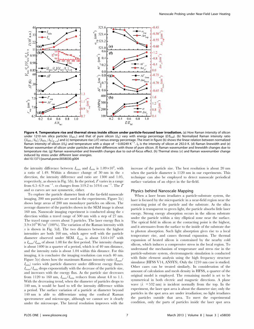
Nanoscale Mapping for Near-Field Heating under 800,400 and 200 nm ParticlesThe experimental method for the 1210 nm case is employed to
attain nanoscale imaging for the 800, 400 and 200 nm cases. The
integration time is 2 s. Four energy levels are also used in the
Raman mapping experiments for 800 and 400 nm cases. Similar
mapping results are observed as in Fig. 3(a). Here we only discuss
the cases under energy level of 3.16109 W/m2 (79%). The results
for the 800 nm case are illustrated in Fig. 5(a). The total travel
range along the x direction is 1.8 mm with a step of 53 nm. More
than two periods are measured. The Imax is 2.246104, 2.826104,
4.186104 and 5.966104 for the four energy percentages of 25%,
50%, 79%, and 100%, respectively. For the 79% case with energy
flux of 3.16109 W/m2, the second intensity period is 853 nm. The
intensity difference and ratio of Imax and Imin are 2.276104 and
2.24, respectively. Within a distance of 30 nm in the x direction,
the intensity difference and ratio are 3400 and 1.10, respectively,
as shown in Fig. 5(a). It indicates that the resolution can be
reached at about 30 nm in this case. In this period, v varies from
518.5 to 519.5 cm21, with a maximum shift of 1.0 cm21. C varies
in a range of 6.5–7.3 cm21, with a maximum difference of
0.8 cm21. The variation curves of v and C along the x direction
are not symmetric, and the reasons are similar with those for the
1210 nm case.
Figure 5(b) shows the variation of silicon Raman intensity along
the x direction for the 400 nm case. The total travel range in the x
direction is 1.2 mm with a step of 27 nm. The Imax is 1.406104,
1.956104, 3.366104 and 4.326104 for the four energy percent-
ages of 25%, 50%, 79%, and 100%, respectively. In the case of
3.16109 W/m2, of which the energy percentage is 79%, the
intensity period lengths are 506 and 453 nm. In the first period,
Nanoscale Probing under Near-Field Laser Heating
PLOS ONE | www.plosone.org 6 March 2013 | Volume 8 | Issue 3 | e58030
the intensity difference between Imax and Imin is 1.096104, with
a ratio of 1.49. Within a distance change of 30 nm in the x
direction, the intensity difference and ratio are 1300 and 1.05,
respectively, as shown in Fig. 5(b). In the period, C varies in a range
from 6.5–6.9 cm21. v changes from 519.2 to 519.6 cm21. The Cand v curves are not symmetric, either.
To explore the particle diameter limit of the far-field nanoscale
imaging, 200 nm particles are used in the experiments. Figure 5(c)
shows large areas of 200 nm monolayer particles on silicon. The
average diameter of the particles shown in the SEM image is about
160 nm. Nanoscale imaging experiment is conducted along the x
direction within a travel range of 500 nm with a step of 27 nm.
The travel range covers about 3 particles. The laser energy flux is
3.96109 W/m2 (100%). The variation of the Raman intensity with
x is shown in Fig. 5(d). The two distances between the highest
intensities are both 160 nm, which agree well with the particle
diameter observed under SEM. Imax is about 3.646104 with
a Imax/Imin of about 1.08 for the first period. The intensity change
is about 1400 in a quarter of a period, which is of 40 nm distance,
and the intensity ratio is about 1.04 within this distance. For this
imaging, it is conclusive the imaging resolution can reach 40 nm.
Figure 5(e) shows how the maximum Raman intensity ratio (Imax/
Imin) varies with particle diameter under different energy fluxes.
Imax/Imin drops exponentially with the decrease of the particle size,
and increases with the energy flux. As the particle size decreases
from 1120 to 160 nm, Imax/Imin reduces from about 4.8 to 1.1.
With the decreasing trend, when the diameter of particles drops to
140 nm, it would be hard to tell the intensity difference within
a period. The surface variation of a particle at diameter beyond
140 nm is able to differentiate using the confocal Raman
spectrometer and microscope, although we cannot see it clearly
under the microscope. The lateral resolution improves with the
increase of the particle size. The best resolution is about 20 nm
when the particle diameter is 1120 nm in our experiments. This
technique can also be employed to detect nanoscale periodical
surface variation of an object in the far-field.
Physics behind Nanoscale MappingWhen a laser beam irradiates a particle-substrate system, the
laser is focused by the microparticle in a near-field region near the
contacting point of the particle and the substrate. As the silica
particle is transparent to green light, the particle absorbs little laser
energy. Strong energy absorption occurs in the silicon substrate
under the particle within a tiny elliptical zone near the surface.
The optical field in silicon at the contacting point is the highest,
and it attenuates from the surface to the inside of the substrate due
to photon absorption. Such light absorption gives rise to a local
temperature rise, and causes thermal expansion. The thermal
expansion of heated silicon is constrained by the nearby cold
silicon, which induces a compressive stress in the local region. To
understand the mechanism of temperature and stress rise in the
particle-substrate system, electromagnetic simulation is conducted
with finite element analysis using the high frequency structure
simulator (HFSS V14, ANSYS). Only the 1210 nm case is studied.
Other cases can be treated similarly. In consideration of the
amount of calculation and mesh density in HFSS, a quarter of the
original model is employed. The remaining model is set to be
symmetrical in both electric and magnetic directions. A plane
wave (l =532 nm) is incident normally from the top. In the
experiment, the laser spot area is about the diameter size; only the
particles in the spot area are under irradiation; no light irradiates
the particles outside that area. To meet the experimental
condition, only the parts of particles inside the laser spot area
Figure 4. Temperature rise and thermal stress inside silicon under particle-focused laser irradiation. (a) How Raman intensity of siliconunder 1210 nm silica particles (ISiO2
) and that of pure silicon (ISi) vary with energy percentage (E/Efull). (b) Normalized Raman intensity ratio( ISiO2
=ISi½ �= ISiO2=ISi½ �E~0) and (c) temperature rise (DT) versus energy percentage. The inset in figure (b) shows the linear relation between normalized
Raman intensity of silicon (I/I0) and temperature with a slope of 20.00249 K21. I0 is the intensity of silicon at 292.0 K. (d) Raman linewidth and (e)Raman wavenumber of silicon under particles and their differences with those of pure silicon. (f) Raman wavenumber and linewidth changes due totemperature rise. (g) Raman wavenumber and linewidth changes due to out-of-focus effect. (h) Thermal stress (s) and Raman wavenumber changeinduced by stress under different laser energies.doi:10.1371/journal.pone.0058030.g004
Nanoscale Probing under Near-Field Laser Heating
PLOS ONE | www.plosone.org 7 March 2013 | Volume 8 | Issue 3 | e58030
remain in the model. Other parts of particles outside the area are
cut off to avoid receiving the plane wave. Perfect H and Perfect E
symmetry boundaries are adopted at symmetrical planes. Absorb-
ing (radiation) boundaries are applied for other boundary planes in
the domain. The electric field amplitude of the incident wave is set
to 1 V/m. Therefore, the near-field enhancement value is the
same as the electric field amplitude of the scattered light. Two
typical cases regarding to different laser-particle positions in an
imaging period are simulated. Figure 6(a) shows the electric field
distributions inside the substrate-particle system for the two cases.
In the left case, the particle center is under the laser spot center,
where the maximum enhancement is achieved in an imaging
period. In the right case, the particle center is at the fringe of the
laser spot, and the enhancement is the minimum in a period. The
highest enhancement values for the two cases are 2.8 and 1.6
inside the substrate, and 6.4 and 4.8 inside the substrate-particle
system. The maximum enhancement ratio of light intensity in the
simulation is only 3.1, smaller than the maximum Raman intensity
ratio in the experiments (4.8). The reasons for the difference will
be discussed later. The laser focusing areas in silicon are right
Figure 5. Nanoscale mapping for different sizes of particles. The Raman intensity I, Raman wavenumber v, and linewidth C for silicon underparticles of (a) 800 nm and (b) 400 nm diameters with laser irradiation. (c) SEM images of 200 nm particles on a substrate. The average diameter ofthe particles is about 160 nm. (d) The Raman intensity of silicon under particles of 200 nm diameter along the x direction. (e) The variation ofmaximum intensity ratio in silicon with particle size under four laser energy fluxes.doi:10.1371/journal.pone.0058030.g005
Nanoscale Probing under Near-Field Laser Heating
PLOS ONE | www.plosone.org 8 March 2013 | Volume 8 | Issue 3 | e58030
beneath the particles which are under laser irradiation, with
a radius of about 200 nm.
The temperature distribution inside the silicon substrate is
modeled using FLUENT (V12.0.1, ANSYS) based on the electric
field distribution. The 1210 nm case with the highest energy and
electric field enhancement is simulated in this work. As the
temperature distribution inside silicon is symmetric, a quarter-
cylinder computational domain with a radius of 5 mm and a height
of 10 mm is considered in the simulation. Both vertical cross-
sections use symmetric boundary conditions. Because the temper-
ature field is measured at steady state, and the heat dissipation via
radiation is small, so the top end surface of silicon is set as
adiabatic. The peripheral and foot end surfaces of the domain and
the initial temperature of the substrate are set at 300 K. The heat
source is imported from the HFSS calculation results. The heat
generation rate per unit volume can be calculated from _qq = Ib,where b =4pk/l is the absorption coefficient, k is the extinction
coefficient, l is the wavelength of incident laser, and
I = P = 0.5ce0nE2 is the laser intensity inside the silicon substrate,
which is equal to the Poynting vector. The light speed in free space
c=36108 m/s, the vacuum permittivity e0 = 8.854610212 F/m,
the refractive index of silicon n=4.15, and E (V/m) the time-
average intensity of the electric field, which is acquired using
HFSS. Other details of the temperature simulation can be found
elsewhere [26]. Figure 6(b) shows the temperature profile inside
silicon from the surface to the bottom under the particle. The inset
illustrates the steady state symmetric temperature distribution on
the surface of the silicon substrate. The calculated maximum
temperature rise inside the silicon is 50.9 K, which is close to the
experimental value (56.1 K).
For the 1210 nm particle case, the maximum enhancement
ratio of light intensity in the simulation is only 3.1, smaller than the
maximum Raman intensity ratio in the experiments (4.8). There
are four main factors considered leading to the differences between
experiments and simulation. The first factor is the relationship
between the collected Raman signal and the distance between the
objective lens and the focusing point, as shown in Fig. 6(c). The
collected Raman signal is the strongest when the focusing point
inside silicon is at the center of the objective lens; see position 1 in
the figure. The signal decreases with the increase of the distance
between focusing location and the lens center during the scanning
process. Position 2 represents a situation that some Raman signals
do not come into the lens through the particle. Instead, they are
missed by the Raman spectrometer. So the amount of collected
Raman signals reduces. As a result, the collected Raman intensity
ratio between position 1 and 2 rises. Second, Raman intensity of
silicon varies with focal level in the vertical direction, as shown in
Fig. 6(d). The Raman intensity reaches maximum at the focal
plane, and decreases with the distance between the sample and
laser focal plane position in the z direction. So the maximum
Raman intensity at the focal plane is much higher than that at an
out-of-focus status. Third, the incident laser employed in the
electric field simulation is a uniform plane wave, while in the
experiments the laser is focused by a 1006objective lens before it
irradiates the sample. Although the laser is still uniformly
distributed in space, the direction of propagation has been
Figure 6. Modeling results and difference illustration. (a) HFSS modeling of a plane wave passing through a 1.21 mm silica sphere (e=2.13+ 0i)in air above a silicon substrate (e= 17.22+0.428i). The amplitude of electric field is equal to the enhancement factor. In the left figure, the particlecenter is under the laser spot center. In the right figure, the particle center is at the fringe of the laser spot area. (b) Temperature profile inside a siliconsubstrate beneath a 1210-nm silica particle under laser irradiation. The inset shows the temperature distribution on the top of the substrate. (c) Howthe collected Raman signal varies with distance between the center of objective lens and laser focusing point in silicon. Position 1 represents thecoincidence of the focusing point and the lens center, and position 2 shows a distance between them. (d) The variation of silicon Raman intensitywith the laser focal level in the vertical direction.doi:10.1371/journal.pone.0058030.g006
Nanoscale Probing under Near-Field Laser Heating
PLOS ONE | www.plosone.org 9 March 2013 | Volume 8 | Issue 3 | e58030
changed. The laser should be focused in an even smaller region by
the particles, which brings up a higher temperature rise in the
focused region. Finally, during the simulation of electromagnetic
field by HFSS, the dimensions of the computational domain are
quite large. The grid is not fine enough, so the precision of the
computational results may drop to a certain extent.
Conclusion
In this work, far-field nanoscale imaging of near-field focusing,
thermal and stress fields in a silicon substrate beneath silica
particles was conducted for the first time using Raman spectros-
copy. Imaging based on the Raman intensity decrease, Raman
wavenumber shift, and linewidth broadening all reflected conju-
gated near-field focusing, thermal, and stress effects. Difference in
the imaging based on these three parameters was largely induced
by the non-coincidence between the laser beam axis and the signal
collecting axis of the Raman spectrometer. Our detailed analysis
revealed that such imaging can achieve a lateral resolution better
than 20 nm (,l/26). The nanoscale imaging capacity was fully
demonstrated by studying the near-field focus under silica particles
from 1210 nm down to 160 nm. Physical methodologies were
developed to separate the near-field focusing, thermal, and stress
effects and evaluate the temperature rise and local stress in
particle-induced near-field focusing. Under 1210 nm silica parti-
cles, the temperature rise in the near-field focusing region in the
silicon substrate reaches 56.1 K under a laser fluence of 3.96109
W/m2, and the local stress is 370 MPa. Our study under different
energy levels revealed that the temperature rise and local stress
increased almost linearly with the energy fluence. The electro-
magnetic and temperature fields inside the substrate-particle
system were simulated to interpret the measured temperature rise
with sound agreement. The imaging method can be used to detect
nanoscale periodical surface variation of an object, and the
thermal and stress variation under the surface in the far-field.
Author Contributions
Supervised the research: XW. Conceived and designed the experiments:
XT XW. Performed the experiments: XT SX. Analyzed the data: XT.
Contributed reagents/materials/analysis tools: XT XW. Wrote the paper:
XT XW.
References
1. Frey HG, Keilmann F, Kriele A, Guckenberger R (2002) Enhancing the
Resolution of Scanning Near-Field Optical Microscopy by a Metal Tip Grown
on an Aperture Probe. Applied Physics Letters 81: 5030–5032.
2. Zenhausern F, Martin Y, Wickramasinghe HK (1995) Scanning Interferometric
Apertureless Microscopy – Optical Imaging at 10 Angstrom Resolution. Science
269: 1083–1085.
3. Taubner T, Korobkin D, Urzhumov Y, Shvets G, Hillenbrand R (2006) Near-
field Microscopy Through a SiC Superlens. Science 313: 1595.
4. Liu ZW, Durant S, Lee H, Pikus Y, Fang N, et al. (2007) Far-field Optical
Superlens. Nano Letters 7: 403–408.
5. Rust MJ, Bates M, Zhuang XW (2006) Sub-Diffraction-Limit Imaging by