81


NanoscaleResearchLettersNanoscaleResLett.9(1):526-526

OverviewofemergingnonvolatilememorytechnologiesJaganSinghMeena1,SimonMinSze1,UmeshChand1,Tseung-YuenTseng1
1.DepartmentofElectronicsEngineeringandInstituteofElectronics,NationalChiaoTungUniversity,Hsinchu30010,Taiwan
Copyright©2014Meenaetal.;licenseeSpringer.
DOI:10.1186/1556-276X-9-526
Publishedonline:25September2014

Abstract
NonvolatilememorytechnologiesinSi-basedelectronicsdatebacktothe1990s.Ferroelectricfield-effecttransistor(FeFET)wasoneofthemostpromisingdevicesreplacingtheconventionalFlashmemoryfacingphysicalscalinglimitationsatthosetimes.AvariantofchargestoragememoryreferredtoasFlashmemoryiswidelyusedinconsumerelectronicproductssuchascellphonesandmusicplayerswhileNANDFlash-basedsolid-statedisks(SSDs)areincreasinglydisplacingharddiskdrivesastheprimarystoragedeviceinlaptops,desktops,andevendatacenters.TheintegrationlimitofFlashmemoriesisapproaching,andmanynewtypesofmemorytoreplaceconventionalFlashmemorieshavebeenproposed.Emergingmemorytechnologiespromisenewmemoriestostoremoredataatlesscostthantheexpensive-to-buildsiliconchipsusedbypopularconsumergadgetsincludingdigitalcameras,cellphonesandportablemusicplayers.Theyarebeinginvestigatedandleadtothefutureaspotentialalternativestoexistingmemoriesinfuturecomputingsystems.Emergingnonvolatilememorytechnologiessuchasmagneticrandom-accessmemory(MRAM),spin-transfertorquerandom-accessmemory(STT-RAM),ferroelectricrandom-accessmemory(FeRAM),phase-changememory(PCM),andresistiverandom-accessmemory(RRAM)combinethespeedofstaticrandom-accessmemory(SRAM),thedensityofdynamicrandom-accessmemory(DRAM),andthenonvolatilityofFlashmemoryandsobecomeveryattractiveasanotherpossibilityforfuturememoryhierarchies.Manyothernewclassesofemergingmemorytechnologiessuchastransparentandplastic,three-dimensional(3-D),andquantumdotmemorytechnologieshavealsogainedtremendouspopularityinrecentyears.Subsequently,notanexaggerationtosaythatcomputermemorycouldsoonearntheultimatecommercialvalidationforcommercialscale-upandproductionthecheapplasticknockoff.Therefore,thisreviewisdevotedtotherapidlydevelopingnewclassofmemorytechnologiesandscalingofscientificproceduresbasedonaninvestigationofrecentprogressinadvancedFlashmemorydevices.

Review
BackgroundGeneraloverview
Theideaofusingafloatinggate(FG)devicetoobtainanonvolatilememorydevicewassuggestedforthefirsttimein1967byKahngDandSzeSMatBellLabs[1].ThiswasalsothefirsttimethatthepossibilityofnonvolatileMOSmemorydevicewasrecognized.Fromthatday,semiconductormemoryhasmadetremendouscontributionstotherevolutionarygrowthofdigitalelectronicssincea64-bitbipolarRAMchiptobeusedinthecachememoryofanIBMcomputerwasreportedin1969[2].Semiconductormemoryhasalwaysbeenanindispensablecomponentandbackboneofmodernelectronicsystems.Allfamiliarcomputingplatformsrangingfromhandhelddevicestolargesupercomputersusestoragesystemsforstoringdatatemporarilyorpermanently[3].Beginningwithpunchcardwhichstoresafewbytesofdata,storagesystemshavereachedtomultiterabytesofcapacitiesincomparativelylessspaceandpowerconsumption.Regardingapplicationaspects,thespeedofstoragesystemsneedstobeasfastaspossible[4].SinceFlashmemoryhasbecomeacommoncomponentofsolid-statedisks(SSDs),thefallingpricesandincreaseddensitieshavemadeitmorecost-effectiveformanyotherapplications[5].MemorydevicesandmostSSDsthatuseFlashmemoryarelikelytoserveverydifferentmarketsandpurposes.Eachhasanumberofdifferentattributeswhichareoptimizedandadjustedtobestmeettheneedsofparticularusers.Becauseofnaturalinherentlimitations,thelong-establishedmemorydeviceshavebeenshortedoutaccordingtotheirinventionstomatchwithportableelectronicdatastoragesystems.Today,themostprominentoneisthelimitedcapacityforcontinuedscalingoftheelectronicdevicestructure.ResearchismovingalongthefollowingpathsforembeddedFlashdevices:(i)scalingdownthecellsizeofdevicememory,(ii)loweringvoltageoperation,and(iii)increasingthedensityofstatepermemorycellbyusingamultilevelcell.Tosustainthecontinuousscaling,conventionalFlashdevicesmayhavetoundergorevolutionarychanges.Basically,itisexpectedthatanentireDVDcollectionbeinthepalmofahand.Noveldeviceconceptswithnewphysicaloperationingprinciplesareneeded.Itisworthwhiletotakealookatsemiconductormemoriesagainstthebackgroundofdigitalsystems.Thewaysemiconductordevicesareusedinasystemsenvironmentdetermineswhatisrequiredofthemintermsofdensity,speed/power,andfunctions.Itisalsoworthwhiletolookintotheeconomicsignificanceofsemiconductormemoriesandtherelativeimportanceoftheirvarioustypes.Forthepastthreeandahalfdecadesinexistence,thefamilyofsemiconductormemorieshasexpandedgreatlyandachievedhigherdensities,higherspeeds,lowerpower,morefunctionality,andlowercosts[3,6,7].Atthesametime,someofthelimitationswithineachtypeofmemoryarealsobecomingmorerealized.Assuch,thereareseveralemergingtechnologiesaimingtogobeyondthoselimitationsandpotentiallyreplaceallormostoftheexistingsemiconductormemorytechnologiestobecomeauniversalsemiconductormemory(USM).Inaddition,therewardsforachievingsuchadevicewouldbetogaincontrolofanenormousmarket,whichhasexpandedfromcomputerapplicationstoallofconsumerelectronicproducts.Lookingforwardtothefuture,therearewiderangesofemergingmemoryapplicationsforautomationand

informationtechnologytohealthcare.Thespecificationofnonvolatilememory(NVM)isbasedonthefloatinggateconfiguration,whichisthefeatureofanerasedgateputintomanycellstofacilitateblockerasure.Amongthem,designedFlashmemoriessuchasNORandNANDFlashhavebeendevelopedandthenproposedascommercialproductsintobulkmarket.Theyhavebeenconsideredasthemostimportantproducts.NORhashighoperationspeedforbothcodeanddatastorageapplications;ontheotherhand,NANDhashighdensityforlargedatastorageapplications[8].SincetheinceptionofFlashmemory,therehasbeenanexponentialgrowthinitsmarketdrivenprimarilybycellphonesandothertypesofconsumerelectronicequipment.While,today,integrationofasiliconchipisnoteconomical,toys,cards,labels,badges,valuepaper,andmedicaldisposablescouldbeimaginedtobeequippedwithflexibleelectronicsandmemory.Withgrowingdemandsforhigh-densitydigitalinformationstorage,memorydensitywitharrivingtechnologyhasbeenincreaseddramaticallyfromthepastcoupleofyears.Themaindrivetodeveloporganicnonvolatilememoryiscurrentlyforapplicationsofthin-film,flexible,orevenprintedelectronics.Oneneedsatechnologytotageverythingtoelectronicfunctionalitywhichcanbeforeseeninaverylargequantityandataverylowcostonsubstratessuchasplasticandpaper.Accessiblepopularizationofroll-to-rollmemorycommercializationisawaytomakeanencounterinterestingandchallengingtohavechargestoragedevicesofchoiceforapplicationswithenormousflexibilityandstrength.Recently,polymer(plasticmemory)andorganicmemorydeviceshavesignificantconsiderationbecauseoftheirsimpleprocesses,fastoperatingspeed,andexcellentswitchingability[9,10].Onesignificantadvantagepolymermemoryhasoverconventionalmemorydesignsisthatitcanbestackedvertically,yieldingathree-dimensional(3-D)useofspace[11].Thismeansthatinterabytesolid-statedeviceswithextremelylowtransistorcountssuchasdrivesaboutthesizeofamatchbook,thedatapersistsevenafterpowerisremoved.TheNANDFlashmarketiscontinuallygrowingbythesuccessiveintroductionofinnovativedevicesandapplications.Tomeetthemarkettrend,3-DNVMsareexpectedtoreplacetheplanarones,especiallyfor10-nmnodesandbeyond.Moreover,simple-structureorganicbistablememoryexhibitingsuperiormemoryfeatureshasbeenrealizedbyemployingvariousnanoparticles(NPs)blendedintoasingle-layeredorganicmaterialsandwichedbetweentwometalelectrodes[12,13].TheNPsactastrapsthatcanbechargedanddischargedbysuitablevoltagepulses.NPblendsshowpromisingdataretentiontimes,switchingspeed,andcyclingendurance,buttheon-statecurrentistoolowtopermitscalingtonanometerdimensions[10,14].Alotofthesegreatideastendtodiebeforereachingthispointofdevelopment,butthatisnottosaythatwewillbeseeingplasticmemoryonstoreshelvesnextyear.Therearestillmanyhurdlestogetover;softwarealoneisabigtask,asisthemanufacturingprocess,butitdoesbringthistechnologyonestepclosertoreality[15].Itisnotanexaggerationtosaythattheequivalentof400,000CDs,60,000DVDs,or126ÂyearsofMPGmusicmaybestoredonapolymermemorychipthesizeofacreditcard.
Thevisionofthisreview
Inthisreview,wefocusonelectricallyprogrammablenonvolatilememorychangesfromsiliconnanocrystalmemoryscalingtoorganicandmetallicNPmemorydevices.Further,thescalingtrendmovetowardstheemergingNVMtoflexibleandtransparentredox-basedresistiveswitchingmemorytechnologies.Thisreviewisintendedtogivean

overviewtothereaderofstoragesystemsandcomponentsfromconventionalmemorydevicesthathavebeenproposedinthepastyearsofrecentprogressincurrentNVMdevicesbasedonnanostructuredmaterialstoredox-basedresistiverandom-accessmemory(RRAM)to3-Dandtransparentmemorydevices.WedescribethebasicsofFlashmemoryandthenhighlightthepresentproblemswiththeissueofscalingtunneldielectricinthesedevices.Webrieflydescribeahistoricalchange,howtheconventionalFGnonvolatilememorysuffersfromachargelossproblemasthefeaturesizeofthedevicecontinuestoshrink.Adiscretepolysilicon-oxide-nitride-oxide-silicon(SONOS)memoryisthenproposedasareplacementoftheconventionalFGmemory.TheNCmemoryisexpectedtoefficientlypreservethetrappedchargeduetothediscretechargestoragenodewhilealsodemonstratingexcellentfeaturessuchasfastprogram/erasespeeds,lowprogrammingpotentials,andhighendurance.Wealsodiscusscurrentongoingresearchinthisfieldandthesolutionsproposedtosolvethescalingproblemsbydiscussingaspecificsolutionindetailwhichwouldbethecenterpieceinrecentmemoryworkprogress.Moreover,thisreviewmakesdistinctemergingmemoryconceptswithmorerecentmolecularandquantumdotprogrammablenonvolatilememoryconcepts,specificallyusingchargetrappinginconjugatedpolymersandmetalNPs.Weclassifyseveralpossibledevices,accordingtotheiroperatingprinciple,andcriticallyreviewtheroleofπ-conjugatedmaterialsinthedatastoragedeviceoperation.WedescribespecificationsforapplicationsofemergingNVMdevicesaswellasalreadyexistingNANDmemoryandreviewthestateoftheartwithrespecttothesetargetspecificationsinthefuture.Conclusionsaredrawnregardingfurtherworkonmaterialsandupcomingmemorydevicesandarchitectures.
Classificationofsolid-statememorytechnologiesDatastoragedevicescanbeclassifiedbasedonmanyfunctionalcriteria.Ofthem,silicon-basedsemiconductormemoriesarecategorizedintotwo:volatileandnonvolatile[3,16].Involatilememories,theinformationeventuallyfadeswhilepowersupplyisturnedoffunlessthedevicesusedtostoredatawillbeperiodicallyrefreshed.Ontheotherhand,nonvolatilememoriesretainthestoredinformationevenwhenthepowersupplyisturnedoff.Volatilememories,suchasstaticrandom-accessmemory(SRAM)anddynamicrandom-accessmemory(DRAM),needvoltagesupplytoholdtheirinformationwhilenonvolatilememories,namelyFlashmemories,holdtheirinformationwithoutone.DRAM(dynamicstandsfortheperiodicalrefresh)isneededfordataintegrityincontrasttoSRAM.ThebasiccircuitstructuresofDRAM,SRAM,andFlashmemoriesareshowninFigureÂ1.DRAM,SRAM,andFlasharetoday’sdominantsolid-statememorytechnologies,whichhavebeenaroundforalongtime,withFlashtheyoungest,at25Âyears.DRAMisbuiltusingonlyonetransistorandonecapacitorcomponent,andSRAMisusuallybuiltinCMOStechnologywithsixtransistors.Twocross-coupledinvertersareusedtostoretheinformationlikeinaflip-flop.Fortheaccesscontrol,twofurthertransistorsareneeded.Ifthewritelineisenabled,thendatacanbereadandsetwiththebitlines.TheFlashmemorycircuitworkswiththeFGcomponent.TheFGisbetweenthegateandthesource-drainareaandisolatedbyanoxidelayer.IftheFGisuncharged,thenthegatecancontrolthesource-draincurrent.TheFGgetsfilled(tunneleffect)withelectronswhenahighvoltageatthegateissupplied,andthenegativepotentialontheFGworksagainstthegateandnocurrentispossible.TheFGcanbe

erasedwithahighvoltageinreversedirectionofthegate.DRAMhasanadvantageoverSRAMandFlashofonlyneedingoneMOSFETwithacapacitor.ItalsohastheadvantageofcheapproductionaswellaslowerpowerconsumptionascomparedtoSRAMbutslowerthanSRAM.Ontheotherhand,SRAMisusuallybuiltinCMOStechnologywithsixtransistorsandtwocross-coupledinverters,andfortheaccesscontrol,twofurthertransistorsareneeded.SRAMhastheadvantageofbeingquick,easytocontrol,integratedinthechip,aswellasfastbecausenobusisneededlikeinDRAM.ButSRAMhasthedisadvantagesofneedingmanytransistorsandhenceexpensive,higherpowerconsumptionthanDRAM.IncomparisontoDRAMandSRAM,FlashmemoryhasFGbetweenthegateandthesource-drainareaandisolatedwithanoxidelayer.FlashmemorydoesnotrequirepowertostoreinformationbutisslowerthanSRAMandDRAM.
Viewlargerversion
Figure1.ThecircuitrystructuresofDRAM,SRAM,andFlashmemories.
BothtypesofmemoriescanbefurtherclassifiedbasedonthememorytechnologythattheyuseandbasedondatavolatilityasshownintheclassificationflowchartdepictedinFigureÂ2.VolatilememoriesconsistmostlyofDRAM[17],whichcanbefurtherclassifiedintoSDRAMandmobileRAMwhichonlyretaininformationwhencurrentisconstantlysuppliedtothedevice[18].AnothersmallbutveryimportantmemorydeviceisSRAM.ThemarketforDRAMdevicesfarexceedsthemarketforSRAMdevices,althoughasmallamountofSRAMdevicesisusedinalmostalllogicandmemorychips.However,DRAMusesonlyonetransistorandonecapacitorperbit,allowingittoreachmuchhigherdensitiesand,withmorebitsonamemorychip,bemuchcheaperperbit.SRAMisnotworthwhilefordesktopsystemmemory,whereDRAMdominates,butisusedforitscachememories.SRAMiscommonplaceinsmallembeddedsystems,whichmightonlyneedtensofkilobytesorless.ForthcomingvolatilememorytechnologiesthathopetoreplaceorcompetewithSRAMandDRAMincludeZ-RAM,TTRAM,A-RAM,andETARAM.Intheindustry,newuniversalandstablememorytechnologieswillappearasrealcontenderstodisplaceeitherorbothNANDFlashandDRAM.Flashmemoryispresentlythemostsuitablechoicefornonvolatileapplicationsforthefollowingreasons:Semiconductornonvolatilememoriesconsistmostlyoftheso-called‘Flash’devicesandretaintheirinformationevenwhenthepoweristurnedoff.Othernonvolatilesemiconductormemoriesincludemaskread-onlymemory(MROM),antifuse-basedone-timeprogrammable(OTP)memory,andelectricallyerasableread-onlymemory(EEPROM).Flashisfurtherdividedintotwocategories:NOR,characterizedbyadirectwriteandalargecellsize,andNAND,characterizedbyapagewriteandsmallcellsize.Nonvolatilememoryisacomputermemorythatcanretainthestoredinformationevenwhennotpowered[3,19,20].Nonvolatilesemiconductormemoriesaregenerallyclassifiedaccordingtotheirfunctionalpropertieswithrespecttotheprogramminganderasingoperations,asshownintheflowchartdescribedinFigureÂ2.Thesearefloatinggate,nitride,ROMandfuse,Flash,emerging,andothernewnext-generationmemorytechnologies.Today,thesenonvolatilememoriesarehighlyreliableandcanbeprogrammedusingasimplemicrocomputerandvirtuallyineverymodernelectronic

equipment,whichareexpectedtoreplaceexistingmemories.
Viewlargerversion
Figure2.Flowchartforthesemiconductormemoryclassificationaccordingtotheirfunctionalcriteria.
Amongthem,emergingnonvolatilememoriesarenowverycaptivating.Thenext-generationmemorymarketwillcoveruptheseemergingmemorytechnologies[21].Therearemainlyfivetypesofnonvolatilememorytechnology:Flashmemory,ferroelectricrandom-accessmemory(FeRAM),magneticrandom-accessmemory(MRAM),phase-changememory(PCM),andRRAM.Nonvolatilememory,specifically‘Flash’memory,whichischaracterizedbyalarge-block(or‘sector’)erasingmechanism,hasbeenthefastestgrowingsegmentofthesemiconductorbusinessforthelast10Âyears.SomeoftheseneweremergingtechnologiesincludeMRAM,FeRAM,PCM,spin-transfertorquerandom-accessmemory(STT-RAM),RRAMandmemristor.MRAMisanonvolatilememory[10,22].UnlikeDRAM,thedataisnotstoredinanelectricchargeflow,butbymagneticstorageelements.Thestorageelementsareformedbytwoferromagneticplates,eachofwhichcanholdamagneticfield,separatedbyathininsulatinglayer.Oneofthetwoplatesisapermanentmagnetsettoaparticularpolarity;theother’sfieldcanbechangedtomatchthatofanexternalfieldtostorememory.STT-RAMisanMRAM(nonvolatile)butwithbetterscalabilityovertraditionalMRAM.TheSTTisaneffectinwhichtheorientationofamagneticlayerinamagnetictunneljunctionorspinvalvecanbemodifiedusingaspin-polarizedcurrent.Spin-transfertorquetechnologyhasthepotentialtomakeMRAMdevicescombininglowcurrentrequirementsandreducedcostpossible;however,theamountofcurrentneededtoreorientthemagnetizationisatpresenttoohighformostcommercialapplications.PCMisanonvolatilerandom-accessmemory,whichisalsocalledovonicunifiedmemory(OUM),basedonreversiblephaseconversionbetweentheamorphousandthecrystallinestateofachalcogenideglass,whichisaccomplishedbyheatingandcoolingoftheglass.Itutilizestheuniquebehaviorofchalcogenide(amaterialthathasbeenusedtomanufactureCDs),wherebytheheatproducedbythepassageofanelectriccurrentswitchesthismaterialbetweentwostates.Thedifferentstateshavedifferentelectricalresistancewhichcanbeusedtostoredata.Theidealmemorydeviceortheso-calledunifiedmemorywouldsatisfysimultaneouslythreerequirements:highspeed,highdensity,andnonvolatility(retention).Atthepresenttime,suchmemoryhasnotbeendeveloped.Thefloatinggatenonvolatilesemiconductormemory(NVSM)hashighdensityandretention,butitsprogram/erasespeedislow.DRAMhashighspeed(approximately10Âns)andhighdensity,butitisvolatile.Ontheotherhand,SRAMhasveryhighspeed(approximately5Âns)butlimitedfromverylowdensityandvolatility.ItisexpectedthatPCMwillhavebetterscalabilitythanotheremergingtechnologies.RRAMisanonvolatilememorythatissimilartoPCM.Thetechnologyconceptisthatadielectric,whichisnormallyinsulating,canbemadetoconductthroughafilamentorconductionpathformedafterapplicationofasufficientlyhighvoltage.Arguably,thisisamemristortechnologyandshouldbeconsideredaspotentiallyastrongcandidatetochallengeNANDFlash.Currently,FRAM,MRAM,andPCMareincommercialproductionbutstill,relativetoDRAMandNANDFlash,remain

limitedtonicheapplications.ThereisaviewthatMRAM,STT-RAM,andRRAMarethemostpromisingemergingtechnologies,buttheyarestillmanyyearsawayfromcompetingforindustryadoption[23].Anynewtechnologymustbeabletodelivermost,ifnotall,ofthefollowingattributesinordertodriveindustryadoptiononamassscale:scalabilityofthetechnology,speedofthedevice,andpowerconsumptiontobebetterthanexistingmemories.TheNVSMisininspiringsearchofnovelnonvolatilememories,whichwillsuccessfullyleadtotherealizationandcommercializationoftheunifiedmemory.
Inprogress,anothernewclassofnonvolatilememorytechnologieswillofferalargeincreaseinflexibilitycomparedtodisks,particularlyintheirabilitytoperformfast,randomaccesses.UnlikeFlashmemory,thesenewtechnologieswillsupportin-placeupdates,avoidingtheextraoverheadofatranslationlayer.Further,thesenewnonvolatilememorydevicesbasedondeoxyribonucleicacid(DNA)biopolymerandorganicandpolymermaterialsareoneofthekeydevicesforthenext-generationmemorytechnologywithlowcost.NonvolatilememorybasedonmetallicNPsembeddedinapolymerhosthasbeensuggestedasoneofthesenewcross-pointmemorystructures.Inthissystem,traplevelssituatedwithinthebandgapofthepolymerareintroducedbytheNPs[24,25].Memorydevicesplayamassiveroleinallemergingtechnologies;assuch,effortstofabricateneworganicmemoriestobeutilizedinflexibleelectronicsareessential.Flexibilityisparticularlyimportantforfutureelectronicapplicationssuchasaffordableandwearableelectronics.Muchresearchhasbeendonetoapplytheflexibleelectronicstechnologytopracticaldeviceareassuchassolarcells,thin-filmtransistors,photodiodes,light-emittingdiodes,anddisplays[26-28].Researchonflexiblememorywasalsoinitiatedforthesefutureelectronicapplications.Inparticular,organic-basedflexiblememorieshavemeritssuchasasimple,low-temperature,andlow-costmanufacturingprocess.Severalfabricationresultsoforganicresistivememorydevicesonflexiblesubstrateshavebeenreported[29,30].Inaddition,withgrowingdemandforhigh-densitydigitalinformationstorage,NANDFlashmemorydensityhasbeenincreaseddramaticallyforthepastcoupleofdecades.Ontheotherhand,devicedimensionscalingtoincreasememorydensityisexpectedtobemoreandmoredifficultinabit-costscalablemannerduetovariousphysicalandelectricallimitations.Asasolutiontotheproblems,NANDFlashmemorieshavingstackedlayersareunderdevelopingextensions[31,32].In3-Dmemories,costcanbereducedbybuildingmultiplestackedcellsinverticaldirectionwithoutdevicesizescaling.Asabreakthroughforthescalinglimitations,various3-Dstackedmemoryarchitecturesareunderdevelopmentandexpectingthehugemarketof3-Dmemoriesinthenearfuture.Withlotsofexpectation,future-generationmemorieshavepotentialtoreplacemostoftheexistingmemorytechnologies.Thenewandemergingmemorytechnologiesarealsonamedtobeauniversalmemory;thismaygiverisetoahugemarketforcomputerapplicationstoalltheconsumerelectronicproducts.
MarketmemorytechnologiesbyapplicationsThesemiconductorindustryhasexperiencedmanychangessinceFlashmemoryfirstappearedintheearly1980s.ThegrowthofconsumerelectronicsmarketurgesthedemandofFlashmemoryandhelpstomakeitaprominentsegmentwithinthesemiconductorindustry.TheFlashmemorieswerecommerciallyintroducedintheearly1990s,andsince

thattime,theyhavebeenabletofollowMoore’slawandthescalingrulesimposedbythemarket.Thereareexpectedmassivechangesinthememorymarketoverthenextcoupleofyears,withmoredensityandreliabletechnologieschallengingthedominantNANDFlashmemorynowusedinSSDsandembeddedinmobileproducts.Server,storage,andapplicationvendorsarenowworkingonnewspecificationstooptimizethewaytheirproductsinteractwithNVM-movesthatcouldleadtothereplacementofDRAMandharddrivesalikeformanyapplications,accordingtoastoragenetworkingindustryassociation(SNIA)technicalworkinggroup[33,34].TheFlashmemorymarketplaceisoneofthemostvibrantandexcitinginthesemiconductorindustry,nottomentiononeofthemostcompetitive.Thecontinuousinventionofnewmemorytechnologiesandtheirapplicationsinthememorymarketalsoincreaseperformancedemands.Thesenewclassesofmemorieswiththelatesttechnologyincreasetheverticaldemandinthefuturememorymarket.Inthenextcomingyears,cumulativepricereductionsshouldbecomedisruptivetoDVDsandharddiskdrives(HDDs),stimulatehugedemand,andcreatenewFlashmarkets.
Thenonvolatilememoriesofferthesystemadifferentopportunityandcoverawiderangeofapplications,fromconsumerandautomotivetocomputerandcommunication.FigureÂ3showsNVSMmemoryconsumptionbyvariousapplicationsintheelectronicsindustrybymarketin2010extendingupwardsfromcomputersandcommunicationtoconsumerproducts[22].Itisnoticedthatthereisafastergrowthrateofthedigitalcellularphonesince1990;thevolumeofproductionhasincreasedby300times,e.g.,from5millionunitsperyeartoabout1.5billionunitsperyear.Nowadays,flexibilityandtransparencyareparticularlyofgreatsignificanceforfutureelectronicapplicationssuchasaffordableandwearableelectronics.Manyadvancedresearchtechnologiesareappliedtoflexibletechnologytobeusedinarealelectronicsarea[35].Althoughsilicon-basedsemiconductormemorieshaveplayedsignificantrolesinmemorystorageapplicationsandcommunicationinconsumerelectronics,now,therecentfocusisturningfromrigidsilicon-basedmemorytechnologyintoasoftnonvolatilememorytechnologyforlow-cost,large-area,andlow-powerflexibleelectronicapplications.Further,thememorymarketforthelongtermiscontinuouslygrowing,evenifwithsomeupsanddowns,andthisisexpectedtocontinueinthecomingyears[36].Sinceinnovationdrivesthesemiconductorindustry,anewtrendwithtransparencyaswellasflexibilityand3-Dtechnologieswillbeattractiveandmovetowardscontinuousgrowthinthenearfuture.
Viewlargerversion
Figure3.VariousNVSMapplicationsintheelectronicsindustrybymarketsizein2010.Reprintedfromref.[22].
SuccessivecreationofnewmobiledevicesleadstothecontinualgrowthofNANDproductsasshowninFigureÂ4.Tomeetthismarketdemand,earlythisyear,30-nmnodetechnologiesareinramping-upphase,20-nmnodetechnologiesareinthephaseoftransitiontomassproduction,anda10-nmnodetechnologyisunderdevelopment.Inaddition,thefuturemarketrequireshigh-speedoperationevenuptoapproximately1,500ÂMB/sinordertosatisfyalargeamountofdatacorrespondence[37].However,high-speedoperationscausehighpowerconsumptionandchiptemperatureincrease,

whichcandeteriorateNANDreliability.Hence,reductionofoperatingvoltageisinevitabletoachievethefutureNAND.Opportunitiesfortheuseof3-Daswellaspolymermemorydesigninmodernelectroniccircuitsarerapidlyexpanding,basedontheveryhighperformanceanduniquefunctionality.However,theirpracticalimplementationinelectronicapplicationswillultimatelybedecidedbytheabilitytoproducedevicesandcircuitsatacostthatissignificantlybelowthatneededtomanufactureconventionalelectroniccircuitsbasedon,forexample,silicon.Ifsuccessful,theselow-costfabricationprocesseswillultimatelyresultintheprintingoflarge-areaorganicelectroniccircuitsonasheetofplasticpaperusingaroll-to-rollmethod,wherelow-temperaturedepositionoforganicsisfollowedbymetaldepositionandpatterninginacontinuous,high-speedprocessanalogous,perhaps,toprocessesusedintheprintingofdocumentsorfabrics.
Viewlargerversion
Figure4.GrowthofNANDFlashmarketupto2014(iSuppli)andtheinterfacespeedofvariousNANDapplications.Reproducedfromref.[37].
Inrecentyears,IDTechExfindsthatthetotalmarketforprinted,flexible,andorganicelectronicswillgrowfrom$16.04billionin2013to$76.79billionin2023andthisgrowingtrendisexpectedtocontinueinthecomingyears(seeFigureÂ5a).ThemajorityofthatisOLEDs(onlyorganic,notprinted)andconductiveinkusedforawiderangeofapplications.Ontheotherhand,stretchableelectronics,logicandmemory,andthin-filmsensorsaremuchsmalleringredientsbuthavinghugegrowthpotentialastheyemergefromR&D[38].Thereportspecificallyaddressesthebigpicturethatover3,000organizationsarepursuingprinted,organic,flexibleelectronics,includingprinting,electronics,materials,andpackagingcompanies.Whilesomeofthesetechnologiesareinusenow-indeedtherearemainsectorsofbusinesswhichhavecreatedbillion-dollarmarkets-othersarecommerciallyembryonic.
Viewlargerversion
Figure5.Marketvolume(a)andglobalflexibledisplaymarketshipmentforecast(b).Reproducedfromrefs.[38,39].
Anotherkeypotentialmarketforprinted/flexibleelectronicsisnext-generationtransparentconductivefilmtoreplacebrittleandexpensiveindiumtinoxide(ITO)intouchscreensanddisplays,lighting,andphotovoltaics.Touchdisplayresearchsaysthatthemarketfornon-ITOtransparentconductorswillbeabout$206millionthisyearandgrowtosome$4billionby2020asshowninFigureÂ5b.‘HighdemandfortouchscreensfornotebookandPCsizedisplayshascreatedashortageofITOtouchsensorssincetheendoflastyeartodrivemoreinterestinthesetechnologies,andthemoreflexibleandpotentiallycheaperreplacementtechnologiesaregettingmoremature,notesJenniferColegrove,presidentandanalyst,whowillspeakattheFlexTechworkshopontransparentconductors.ShenotesthatAtmel,Fujifilm,UnipixelandCambriosareallinsomephaseofproductionâ

€™[39].Alargeamountofthesemiconductormarket(approximately20%)isgivenbythesemiconductormemories;thus,themarketforchipswilldevelopinthenextfewyears.Thisstudyreportsthatthereisananalysisoftheproductionprocessandthesubsequentvaluechain,whichcomprisesabenchmarkanalysisofthemainsegmentsofthesemiconductorindustry.
Recently,the3-DnonvolatilememorystructurehasalsoattractedconsiderableattentionduetoitspotentialtoreplaceconventionalFlashmemoryinnext-generationNVMapplications[37,40].3-Dmemoriesaregatheringincreasingattentionasfutureultra-high-densitymemorytechnologiestokeepatrendofincreasingbitdensityandreducingbitcost.TheNANDFlashmarketiscontinuouslygrowingbythesuccessiveintroductionofinnovativedevicesandapplications.Tomeetthemarkettrend,3-DNVMsareexpectedtoreplacetheplanarone,especiallyfor10-nmnodesandbeyond.Therefore,thefundamentalsandcurrentstatusofthe3-DNANDFlashmemoryarereviewedandfuturedirectionsarediscussed[41].3-DintegrationpromisestobeanexcellentreplacementofcurrenttechnologiesforthedevelopmentofNANDFlashmemory.TimeisrunningoutforplanarNANDtechnology.ItwillnotbelongthatplanarNANDwillbecompletelyreplacedby3-DNAND.3-DNANDpromisestosatisfythegrowingneedofNANDmemory[37].
Finally,NVMtechnologieshaveabrightfuturesinceeveryend-useapplicationneedstostoresomeparametersorsomeamountofanapplicationprogramintheon-boardNVMtoenableittofunction.TheupcomingNVMsarethebighopeforasemiconductormemorymarket,whichprovidesmemoriesforsystemstorunwithflexibility,reliability,highperformance,andlowpowerconsumptioninatinyfootprintinnearlyeveryelectronicapplication.Recentmarkettrendshaveindicatedthatcommercializedornear-commercializedcircuitsareoptimizedacrossspeed,density,powerefficiency,andmanufacturability.Flashmemoryisnotsuitedtoallapplications,havingitsownproblemswithrandom-accesstime,bitalterability,andwritecycles.Withtheincreasingneedtolowerpowerconsumptionwithzero-powerstandbysystems,observersarepredictingthatthetimehascomeforalternativetechnologiestocaptureatleastsomeshareinspecificmarketssuchasautomotivesmartairbags,high-endmobilephones,andRFIDtags.AnembeddednonvolatilememorywithsuperiorperformancetoFlashcouldseewidespreadadoptioninsystem-on-chip(SoC)applicationssuchassmartcardsandmicrocontrollers.
EmergingNVMtechnologiesforapplicationsThenewemergingnonvolatilerandom-accessmemoryproductsaddresstheurgentneedinsomespecificandsmall-formdevices.Therefore,iRAPfeltaneedtodoadetailedtechnologyupdateandmarketanalysisinthisindustry[42].Recently,YoleDéveloppementreportsdescribethatemergingmemorytechnologieshavegreatpotentialtoimprovefuturememorydevicestobeincreasinglyusedinvariousmarketsofindustryandtransportation,enterprisestorage,mobilephones,massstorage,andsmartcards[43].EmergingNVMapplicationsinvariousmarketsareshowninFigureÂ6.Buttherearenumerousopportunitiesexistingfornovelarchitecturesandapplicationsthattheseemergingmemorytechnologiescanenable.ThesenewemergingNVMproductsaddresstheurgentneedinsomespecificandsmall-formdevices.Therefore,emergingnonvolatilememoryproductsprovidemarketdataaboutthesizeofgrowthofthe

applicationsegmentsandthedevelopmentsofbusinessopportunities.Untilnow,onlyFeRAM,PCM,andMRAMwereindustriallyproducedandavailableinlow-densitychipstoonlyafewplayers.Thus,themarketwasquitelimitedandconsiderablysmallerthanthevolatileDRAM-andnonvolatileFlashNAND-dominantmarkets(whichenjoyedcombinedrevenuesof$50+billionin2012).However,inthenext5Âyears,thescalabilityandchipdensityofthosememorieswillbegreatlyimprovedandwillsparkmanynewapplicationswithNVMmarketdriversexplainedinmoredetail.
Viewlargerversion
Figure6.EmergingNVMapplicationsinvariousmarkets.
AccompaniedbytheadoptionofSTT-MRAMandPCMcachememory,enterprisestoragewillbethelargestemergingNVMmarket.NVMwillgreatlyimprovetheinput/outputperformanceofenterprisestoragesystemswhoserequirementswillintensifywiththegrowingneedforweb-baseddatasupportedbyfloatingmassservers.Inaddition,mobilephoneswillincreasetheiradoptionofPCMasasubstitutetoFlashNORmemoryinMCPpackagesto1-gigabyte(GB)chipsmadeavailablebyMicronin2012.Higher-densitychips,expectedin2015,willallowaccesstosmartphoneapplicationsthatarequicklyreplacingentry-levelphones.STT-MRAMisexpectedtoreplaceSRAMinSoCapplications,thankstolowerpowerconsumptionandbetterscalability.Smartcardsandmicrocontrollers(MCU)willlikelyadoptMRAM/STT-MRAMandPCMasasubstitutetoembedFlash.Indeed,Flashmemorycellsizereductionislimitedinthefuture.TheNVMcouldreducethecellsizeby50%andthusbemorecost-competitive.Additionalfeatureslikeincreasedsecurity,lowerpowerconsumption,andhigherendurancearealsoappealingNVMattributes.ThemassstoragemarketsservedbyFlashNANDcouldbeginusing3-DRRAMin2017to2018,when3-DNANDwillslowdownitsscalabilityaspredictedbyallofthemainmemoryplayers.Ifthishappens,thenamassiveRRAMramp-upwillcommenceinthenextdecadethatwillreplaceNAND;conditional3-DRRAMcost-competitivenessandchipdensityareavailable.ItisexpectedsurelythattheemergingNVMbusinesswillbeverydynamicoverthenext5Âyears,thankstoimprovementsinscalability/costanddensityofemergingNVMchips[44].AccordingtoarecentlypublishedreportfromYoleDéveloppement,EmergingNon-volatileMemoryTechnologies,IndustryTrendsandMarketAnalysis,theglobalmarketforemergingnonvolatilerandom-accessmemoryproductswasprojectedtohavereached$200millionin2012.Thismarketisexpectedtoincreaseto$2,500millionby2018atanaverageannualgrowthataCAGRof+46%throughtheforecastperiodwithmobilephones,smartcards,andenterprisestorageasmaingrowthdrivers(FigureÂ7).Marketadoptionofmemoryisstronglydependentonitsscalability.ThisYoleDéveloppementreportprovidesaprecisememoryroadmapintermsoftechnologicalnodes,cellsize,andchipdensityforeachemergingNVMsuchasFeRAM,MRAM/STT-MRAM,PCM,andRRAM.Amarketforecastisprovidedforeachtechnologybyapplication,units,revenues,andalsomarketgrowthasgivenadetailedaccountofemergingNVMmarketforecast(FigureÂ7).PCMdevices,thedensestNVMin2012at1ÂGB,willreach8ÂGBby2018,whichareexpectedtoreplaceNORFlashmemoryinmobilephonesandwillalso

beusedasastorageclassmemoryinenterprisestorage.MRAM/STT-MRAMchipswillreach8to16ÂGBin2018.TheywillbewidelysoldasastorageclassmemoryandpossiblyasaDRAMsuccessorinenterprisestorageafter2018.By2018,MRAM/STT-MRAMandPCMwillsurelybethetoptwoNVMonthemarket.Combined,theywillrepresenta$1.6billionbusinessby2018,andtheirsaleswillalmostdoubleeachyear,withdouble-densitychipslaunchedevery2Âyears.FeRAMwillbemorestableintermsofscalability,with8-to16-MBchipsavailableby2018;thedevelopmentofanewFRAMmaterialcouldraisescalability,butwedonotexpectittobewidelyindustrializedandcommercializedbefore2018.FeRAMwillgrowatasteadygrowthrate(10%peryear)andwillfocusonindustrialandtransportationapplicationsbecauseofthelow-densityavailability,whereasRRAMrevenueswouldnotreallysurgeby2018,withtheavailabilityofhigh-densitychipsofseveraltensofgigabytesthatcouldreplaceNANDtechnology.Meanwhile,ithasalsobeenconsideredbymemorytechnologistexpertsthatforlarge-volumemarketslikemassstorageNAND,onlyonetechnologywillbeadoptedinordertoreduceproductioncostandRRAMseemstobethebestcandidate.ButtherealmassiveadoptionofemergingNVMasareplacementforNANDandDRAMwillhappenafter2020.
Viewlargerversion
Figure7.EmergingNVMmarketforecastbyapplicationsfrom2012to2018(inM$).Reproducedfromref.[43].
AdvancesinFlashmemorytechnologiesFlashmemoryisbasicallyaMOSFETnonvolatiledevicethatcanbeelectricallyerasedandreprogrammed[3,45].ItisatechnologythatisprimarilyusedinmemorycardsandFlashdrivesforgeneralstorageandtransferofdatabetweencomputersandotherdigitalproducts.Sincetheinventionofthetransistor,NVSMhadbeenthemostimportantinventionintheelectrondevicefield.Thefloatinggatememorywasusedtostoretheinformationandatunnelingcurrentforprogramminganderasingoperations.Thechargeisinjectedintoorremovedfromthefloatinggateandthefloatinggateremainsinthatstate,evenafterpowerisremoved,whichmeansthatFlashmemoryisnonvolatile.TheinventionofNVSMfurthergaverisetoanewclassofmemorydevicesandhencebroadeneditsapplicationstobecomeubiquitous.TherearealargenumberofproductsinthemarketnowwhichuseFlashdevicesexclusivelyassecondarystorage.Fewexamplesoftheirapplicationsincludemedicaldiagnosticsystems,notebookcomputers,digitalaudioplayers,digitalcameras,mobilephones,personaldigitalassistants,digitaltelevisions,universalserialbus(USB)Flashpersonaldisks,GlobalPositioningSystems,andmanymore.Semiconductorstoragedevicesstoredataintinymemorycellsmadeofverysmalltransistorsandcapacitorsmadeofsemiconductormaterialssuchassilicon.Eachcellcanhold1bitofinformationandanarrayofcellsstoresalargechunkofinformation.Flashdevicesaregainingpopularityoverconventionalsecondarystoragedeviceslikeharddisks.TheFlashmemoryfabricationprocessiscompatiblewiththecurrentCMOSprocessandisasuitablesolutionforembeddedmemoryapplications.A

FlashmemorycellissimplyaMOSFETcell,exceptthatapolysiliconfloatinggate[46](orasiliconnitridechargetraplayer)issandwichedbetweenatunneloxideandaninter-polyoxidetoformachargestoragelayer[47].AlthoughFlashmemoryislikelythestandardchargestoragedeviceforthenextgeneration,scalingmayeventuallybelimitedbythetunneloxidelimit[8].Intermsoftheoperationspeedofprogramanderase,Flashmemoryrequiresathintunneloxidetoenhancethecarriertransportbetweenthefloatinggateandthesiliconsubstrate.However,theverythintunneloxidesuffersfrommanyreliabilityissueslikereductioninoperationvoltage,andafteraconsiderablenumberofprogramanderasecycles,thetunneloxideundergoesdeteriorationloss[48].Thus,researchershavefocusedonpossiblesolutionsandproposedalternatetechnologies,includingnitride-basedmemory,nanocrystalmemory,andswitchingmemory.AllothernonvolatilememoriesrequireintegrationofnewmaterialsthatarenotascompatibleastheconventionalCMOSprocess.
NORandNANDFlashmemorytechnologies
NORandNANDFlash,twomajorFlashtypes,aredominantinthememorymarket.NORFlashhaslowerdensitybutarandom-accessinterface,whileNANDFlashhashigherdensityandinterfaceaccessthroughacommandsequence[49].TheircorrespondingstructuresareshowninFigureÂ8.NORandNANDFlashcomefromthestructureusedfortheinterconnectionsbetweenmemorycells.Intelisthefirstcompanytointroduceacommercial(NORtype)Flashchipin1988,andToshibareleasedtheworld’sfirstNANDFlashin1989[50].Dependingonhowthecellsareorganizedinthematrix,itispossibletodistinguishbetweenNANDFlashmemoriesandNORFlashmemories.InNORFlash,cellsareconnectedinparalleltothebitlines,whichnotablyallowthecellstobereadandprogrammedindividually.TheparallelconnectionofNORFlashcellsresembletheparallelconnectionoftransistorsinaCMOSNORgatearchitecture.Ontheotherhand,inNANDFlash,thecellsareconnectedinseries,resemblingaNANDgate.Theseriesconnectionsconsumelessspacethantheparallelones,reducingthecostofNANDFlash.Itdoesnot,byitself,preventNANDcellsfrombeingreadandprogrammedindividually.Mostoftheengineersandscientistsarenotsofamiliarwiththedifferencesbetweenthesetwotechnologies.Generally,theyusuallyrefertotheNORarchitectureas‘Flash’andareunawareoftheNANDFlashtechnologyanditsmanybenefitsoverNOR[51].ThiscouldbeduetothefactthatmostFlashdevicesareusedtostoreandruncodes(usuallysmall),forwhichNORFlashisthedefaultchoice,althoughweareprovidingsomemajordifferencesbetweenNORandNANDFlashtechnologiesbytheirarchitectureandtheinternalcharacteristicfeaturesoftheindividualFlash.
Viewlargerversion
Figure8.ComparisonofNORFlasharrayandNANDFlasharrayarchitectures.
NORFlashisslowerineraseoperationandwriteoperationcomparedtoNANDFlash[52].ThismeansthatNANDFlashhasfastereraseandwritetimes.Moreover,NANDFlashhassmallereraseunits,sofewererasesareneeded.NORFlashcanreaddataslightlyfasterthanNANDFlash.NORFlashofferscompleteaddressanddatabusesto

randomlyaccessanyofitsmemorylocations(addressabletoeverybyte).ThismakesitasuitablereplacementforolderROMBIOS/firmwarechips,whichrarelyneedstobeupdated.Itsenduranceis10,000to1,000,000erasecycles.NORFlashishighlysuitableforstoringcodesinembeddedsystems.Mostoftoday’smicrocontrollerscomewithbuilt-inFlashmemory[53].
NANDFlashoccupiesasmallerchipareapercell.ThismakesNANDFlashavailableingreaterstoragedensitiesandatlowercostsperbitthanNORFlash.ItalsohasuptotentimestheenduranceofNORFlash.NANDismorefitasstoragemediaforlargefilesincludingvideoandaudio.USBthumbdrives,SDcards,andMMCcardsareofNANDtype[54].NAND’sadvantagesarefastwrite(program)anderaseoperations,whileNOR’sadvantagesarerandomaccessandbytewritecapability.NOR’srandomaccessabilityallowsforexecuteinplace(XiP)capability,whichisoftenarequirementinembeddedapplications.NANDisslowrandomaccessible,whileNORishamperedbyhavingslowwriteanderaseperformance.NANDisbettersuitedforfilingapplications.However,moreprocessorsincludeadirectNANDinterfaceandcanbootdirectlyfromNAND(withoutNOR).However,NANDcannotperformreadandwriteoperationssimultaneously;itcanaccomplishtheseatasystemlevelusingamethodcalledshadowing,whichhasbeenusedonPCsforyearsbyloadingtheBIOSfromtheslowerROMintothehigh-speedRAM.
TableÂ1highlightsthemajordifferencesbetweenNORandNAND.ItshowsthatNANDisidealforhigh-capacitydatastoragewhileNORisbestusedforcodestorageandexecution,usuallyinsmallcapacities.Therearemanyotherdifferencesbetweenthesetwotechnologieswhichwillbefurtherdiscussedindividually.However,thoselistedinthetableareenoughtostronglydifferentiatethetypesofapplicationsusingthem:NORistypicallyusedforcodestorageandexecution.This,mainlyincapacitiesupto4ÂMB,iscommoninapplicationssuchassimpleconsumerappliances,low-endcellphones,andembeddedapplications,whilerawNANDisusedfordatastorageinapplicationssuchasMP3players,digitalcameras,andmemorycards[55-57].ThecodesforrawNAND-basedapplicationsarestoredinNORdevices.
Seefulltable
Table1.ComparisonbetweenNORandNANDFlashmemories[55-57]
ScalingandchallengesofFlashmemorytechnologies
Currently,therehavebeenincreasingdemandsonreducingthefeaturesizeinmicroelectronicproductsandmoreinterestinthedevelopmentofFlashmemorydevicestomeetthegrowingworldwidedemand.AconventionalFGmemorydevicemusthaveatunneloxidelayerthicknessof8Ânmtopreventchargelossandtomake10Âyears’dataretentioncertain.ThisnecessitywilllimitscalabilityforFlashmemorydevices[8,58].Thus,inordertomeettechnologyscalinginthefieldofmemoryanddatastoragedevices,

mainstreamtransistor-basedFlashtechnologieswillbedevelopedgraduallytoincorporatematerialandstructuralinnovations[59].Dielectricscalinginnonvolatilememorieshasbeenreachedneartothepointwherenewapproacheswillberequiredtomeetthescalingrequirementswhilesimultaneouslymeetingthereliabilityandperformancerequirementsforfutureproducts.High-dielectric-constantmaterialsarebeingexploredaspossiblecandidatestoreplaceboththetraditionalSiO2andoxide/nitride/oxide(ONO)filmsusedinFlashmemorycells.FlashcellscalinghasbeendemonstratedtobereallypossibleandtobeabletofollowMoore’slawdowntothe90-nmtechnologygenerations.Thetechnologydevelopmentandtheconsolidatedknow-howareexpectedtosustainthescalingtrenddowntothe50-nmtechnologynodeandbelowasforecastedbytheInternationalTechnologyRoadmapforSemiconductors(ITRS)inFigureÂ9,whichindicatesthatthesiliconMOSFETwasalreadyinthenanoscale.TheminimumfeaturesizeofanindividualCMOSFEThasshrunkto15Ânmwithanequivalentgateoxidethickness(EOT)of0.8Ânmin2001[13].However,semiconductorFlashmemoryscalingisfarbehindCMOSlogicdevicescaling.Forexample,theEOTofthegatestackinsemiconductorFlashmemoryisstillmorethan10Ânm.Moreover,semiconductorFlashmemorystillrequiresoperationvoltagesofmorethan10ÂV,whichisstillfarfromtheoperationvoltageofCMOSlogicdevices.ItisimportanttoscaletheEOTofthegatestacktoachieveasmallmemorycellsizeandalsoprolongbatterylife.
Viewlargerversion
Figure9.ThetrendofMOSFETscalingfromITRS.ReproducedfromITRSCorp.
AnotherlimitationofFGtechnologyisthattunneloxidescalingislimitedbystress-inducedleakagecurrent(SILC)relatedtochargetransferproblemasindicatedinFigureÂ10[60,61].TheSILKincreaseswithdecreasingoxidethickness.Thiscanbeattributedtotunnelingassistedbythetrapsinthebulkofthedielectric.Trap-assistedtunnelingcantakeplaceatverylowelectricfields.Ifthedensityoftrapsisincreased,theleakagewillalsoincrease.Electricalstresscanincreasethenumberofthesetraps.Soitbecomesanimportantlimitationofscalingdownthememorydevice[62].ForEOT < 8Ânm,asingleoxidetrapwillcausetocompletethechargelossintheFGFlashcell.Thescalingofthegatestacksandoperationvoltagesareoftenrelatedtoeachother.Atunneloxidethicknessofmorethan8ÂnmiscurrentlyusedinthecommercialFlashmemorychiptomeetthe10Âyears’dataretentiontimerequirement.Ifthetunneloxideweretobescaledbelow2Ânm,theoperationvoltagecouldbereducedfrommorethan10ÂVtobelow4ÂV[63].Unfortunately,theretentiontimewouldalsobereduced,from10Âyearstoseveralseconds.Thisphysicaldamagetothetunneloxideduringthecyclingprocesscausesdataretentionproblems,programdisturbance,readdisturbance,anderraticcharacteristicbehavioroftheFGmemorycell.Suchproblemsseverelylimitthereliabilityandmultilevelcelloperation.Thisbasiclimitationofthetunneloxidethicknessbecomesincreasinglyimportantwithscaling.Newstoragenodeconceptsarealsobecomingattractiveasanalternativeapproachtoaddresssomeofthedielectricscalinglimitations.Flashmemoryadoptsachargestoredinasiliconnitrideasthetrappinglayer,whichexhibitssignificantlyreduceddefect-relatedleakagecurrentandverylowSILCas

comparedtoSiO2withasimilarEOT[64].Sucharelentlessreductionofdevicedimensionshasmanychallengeslikeretention,endurance,reductioninthenumberofelectronsintheFG,dielectricleakage,cell-to-cellcrosstalk,thresholdvoltageshift,andreductioninmemorywindowmargins[65,66].ThekeyconceptofrealscalingissuessuchasmaterialandstructuralchangesinFlashmemorytechnologiesisprovidedindetailinthenextdistinctpart.
Viewlargerversion
Figure10.SchematicplotsofaFlashmemorycellandthedegradationofitstunneloxide.ThedegradationleadstotheformationofpercolationpathsresponsiblefortheFGchargeloss,hencethelossofthestoredinformation.Thepresenceoftrapsintheenergybarrieryieldsthetrap-assistedtunneling
mechanismandoriginatesthestress-inducedleakagecurrent(SILC).
FGFlashmemorytechnology
TheFGNVmemoryisabasicbuildingblockofFlashmemory,whichisbasedonFGthin-filmstorage(TFS)memoriesthathavebeendevelopedwiththeadditionofanerasegateconfiguration.TheconventionalFGmemory(FigureÂ11a)consistsofaMOSFETconfigurationthatismodifiedtoincludepolysiliconasachargestoragelayersurroundedbyaninsulatedinnergate(floatinggate)andanexternalgate(controlgate).ThiswhatmakesFlashmemorynonvolatileandallfloatinggatememoriestohavethesamegenericcellstructure.Chargeistransferredtoorfromthefloatinggatethroughathin(8to10Ânm)oxide[1,67].Becausethefloatinggateiselectricallyisolatedbytheoxidelayer,anyelectronsplacedonitaretrappedthere.Flashmemoryworksbyadding(charging)orremoving(discharging)electronstoandfromafloatinggate.Abit’s0or1statedependsuponwhetherornotthefloatinggateischargedordischarged.Whenelectronsarepresentonthefloatinggate,currentcannotflowthroughthetransistorandthebitstateis‘0’.Thisisthenormalstateforafloatinggate.Whenelectronsareremovedfromthefloatinggate,currentisallowedtoflowandthebitstateis‘1’.TheFGmemoryhasachievedhighdensity,goodprogram/erasespeed,goodreliability,andlowoperatingvoltageandpromotesenduranceforFlashmemoryapplication.
Viewlargerversion
Figure11.SchematicsoftheconventionalFGmemoryandSONOS.Schematicsof(a)floatinggateandthin-filmstorage-basedembeddednonvolatilememorybitcells,dependingonthechargestoredinsidethegatedielectricofaMOSFET,and(b)thenitride
traps(SONOS),embeddedintothegateoxideofaMOSFET.
SONOSmemorytechnology
InordertosolvethescalingissueoftheFGmemory,theSONOSmemoryhasbeenproposedasaFlashtechnologysincethe1980s[68,69].TheacronymSONOSisderivedfromthestructureofthedeviceasshowninFigureÂ11b.TheSONOSdeviceisbasicallyaMOSFET,wherethegatehasbeenreplacedbyanONOdielectric.TheSONOSmemoryhasabetterchargeretentionthantheFGmemorywhentheFGbitcell’stunnelingoxidelayerisbelow10Ânm[70].Moreover,theSONOSmemoryexhibitsmanyadvantages,e.g.,easytofabricate,highprogram/erase(P/E)speed,lowprogrammingvoltageand

powerconsumption,andbetterpotentialforscalabilitybelowthe70-nmnode,accordingtotheITRS[71].Thecharge,holesorelectrons,areinjectedintothenitridelayerusingdirecttunnelingthroughthetunneloxidelayer.Thenitridelayeriselectricallyisolatedfromthesurroundingtransistor,althoughchargesstoredonthenitridedirectlyaffecttheconductivityoftheunderlyingtransistorchannel.SincetheSONOSmemorypossessesspatiallyisolateddeep-leveltraps,asingledefectinthetunnelingoxidewillnotcausedischargeofthememorycell.ThethicknessofthetopoxideisimportanttopreventtheFowler-Nordheimtunnelingofelectronsfromthegateduringerase.Whenthepolysiliconcontrolgateisbiasedpositively,electronsfromthetransistorsourceanddrainregionstunnelthroughtheoxidelayerandgettrappedinthesiliconnitride.Thisresultsinanenergybarrierbetweenthedrainandthesource,raisingthethresholdvoltageVth(thegate-sourcevoltagenecessaryforcurrenttoflowthroughthetransistor).Moreover,thenitridelayeriselectricallyisolatedfromthesurroundingtransistor,althoughchargesstoredonthenitridedirectlyaffecttheconductivityoftheunderlyingtransistorchannel.Theoxide/nitridesandwichtypicallyconsistsofa2-nm-thickoxidelowerlayer,a5-nm-thicksiliconnitridemiddlelayer,anda5-to10-nm-thickoxideupperlayer[72,73].However,SONOS-typeFlashmemorieshaveseveraldrawbackssuchasshallowtrapenergylevel,erasesaturation,andverticalstoredchargemigration[74].Theprogrammingspeedandoperatingvoltageproblemscanbesolvedbyreducingthetunneloxidethickness.Atlowtunneloxidethickness,theissuesthatimpactSONOS-typememoriesincludeerasesaturationandverticalchargemigration,whichseriouslydegradetheretentioncapabilityofthememory[75].Thus,manyconcernsstillremainfortheSONOStypeofmemories,whichwillbediscussedinthenextsection.
LimitationsofFGandSONOSmemorytechnologies
Scalingdemandsverythingateinsulatorsinordertokeepshortchanneleffectsandcontroltheshrinkageofthedevicesizeandmaximizetheperformance.Whenthetunnelingoxidethicknessisbelow10Ânm,thestoragedchargeintheFGiseasytoleakduetoadefectinthetunnelingoxideformedbyrepeatedwrite/erasecyclesordirecttunnelingcurrent.
ThetunnelinggateoxidethicknessinaconventionalFlashmemorycannotbescaleddowntosub-7Ânmbecauseofchargeretention[76].TheSONOSFlashmemorycanrelievetheproblembutstillhasarelativelythickgatedielectricthicknessofabout7Ânm.Therefore,conventionalSONOSFlashmemoryalsohasascaling-downproblem.ManystudieshaveshownthatthechargeretentioncharacteristicsinscaledSONOSnonvolatilememorydeviceswithalowgateoxidethicknessandathightemperatureareproblematicwithshallow-leveltraps[48,77,78].FortheconventionalSONOSmemory,erasesaturationandverticalstoredchargemigration[79,80]arethetwomajordrawbacks;themostchallengingtasksarehowtomaintainanacceptablechargecapabilityofthediscretestoragenodesandhowtofabricatenanocrystalswithconstantsize,highdensity,anduniformdistributions[81].Whenthetrapenergylevelisshallow,erasesaturationandverticalmigrationoccurandtheelectronchargedecayrateincreasesduetolowtunneloxidethickness,issuesthatimpactSONOS-typememoriesasshowninFigureÂ12.ThiserasesaturationmakesSONOSeraselessastheerasevoltageorthetunneloxidethicknessisincreased.SincetheSONOSmemoryusessiliconnitrideasachargetrappinglayer,theelectronsintheSisub-conductionbandwilltunnelthroughthetunnelingoxide

andaportionofthenitride,andthisconsequentlydegradestheprogramspeed.Besidesthis,theconductionbandoffsetofnitrideisonly1.05ÂeVandback-tunnelingofthetrappedelectronmayalsooccur.Althoughapplyingaveryhighelectricfieldmayacceleratethede-trappingrate,thegateelectroninjectioncurrentexceedsthede-trappingbutresultinginpracticallyanincreaseinchargeandnoerasing.Usinganultra-thin(<2Ânm)tunneloxideoffersanefficientchargedirecttunnelingeraseandopensamemorywindow.However,thedirecttunnelingcannotbeturnedoffatalowelectricfield,leadingtopoorretentionandreaddisturb.Thus,theSONOSmemorycannotbeusedforNANDFlashwithoutfurtherinnovationofnewmemorytechnologies.ThemainreasonforthegrowthofemergingNVMtechnologiesisthatscalinghasnowbecomeaseriousissueforthememoryindustry.Notonlyaremanyofthesenewtechnologiesinherentlymorescalable,butalsotheyseemwellsuitedtothenextgenerationofmobilecomputingandcommunicationsthatwilldemandhigh-capacitymemoriescapableofstoringandrapidlyaccessingvideoandalargedatabasewithoutoverburdeningbatterypowersources.
Viewlargerversion
Figure12.Fowler-Nordheim(FN)tunnelingofelectronsfromthegateduringeraseanderasesaturationinSONOSnonvolatilememory.Thisindicatesthereducedmemorywindowastheerasevoltageisincreased.Reproducedfromref.[74].
Manyalternatedevicestructuresareproposedtohopefullycircumventthesescalingchallengesandtoimprovethedeviceperformance.InanefforttocontinueMoore’slawandovercometheultimatelimitationsofMOS-basedmemorydevices,otherstorageconceptshavebeenproposedinsearchofthe‘unifiedmemory’.Theidealmemorydeviceortheso-called‘unifiedmemory’wouldsatisfysimultaneouslythreerequirements:highspeed,highdensity,andnonvolatility.Atthepresenttime,suchanidealmemoryhasnotbeendeveloped.FGNVSMhashighdensityandnonvolatility,butitsP/Espeedislow.DRAMhashighspeed(approximately10Âns)andrelativelyhighdensity,butitisvolatile.SRAMhasveryhighspeed(approximately5Âns),butitsuffersfromverylowdensityandvolatility.Manynonvolatilememorydeviceshavebeenproposedonthebasisofchangingchargestoragematerialsandnewdeviceconceptsforthe‘unifiedmemory’.Thesestructureswillbeconsideredinthenextsections.Inlightofsuchissues,emergingmemorysolutionsseemtobeakeytechnology.
CurrentemergingmemorytechnologiesRecentstudieshaverevealedthatthereisaclosecorrelationamongexistingandemergingmemorytechnologiesinviewofscalability.Thescalingtrendofmemorytransitionleadstosmallerandsmallermemorydevices,whichhavebeenroutinelyobserved.Tofurthersupportthisassertion,anothersetofcurrentprogressinmemorytechnologyisdescribedtotheincreasingimportanceofmemorytousers’experienceandtheimportanceofmemorytosystemperformance.Therearemanyemergingmemorytechnologieswhicharetryingtoreplaceexistingmemorytechnologiesinthemarket.ThesenewmemorydevicessuchasRRAM,PCM,andSTT-RAMhaveread/write/retention/endurancecharacteristicsdifferentfromthoseofconventionalSRAM,DRAM,andFlash[82].But

theidealcharacteristicsofnewemergingmemorytechnologieshavetobemeetingtheperformanceofSRAMandthedensityofNANDFlashintermsofstability,scalability,andswitchingspeed.Thus,goingbeyondthetraditionalbistablememory,thepossibilitiesofmultilevel,high-performancememorydevicessuitableformarketmustbeexplored.Currently,thereareseveraltechnologiesthatshowsomepromise;someofthesenewemergingtechnologiesareMRAM,FeRAM,PCM,STT-RAM,nano-random-accessmemory(NRAM),racetrackmemory,RRAMandmemristor,molecularmemory,andmanyothers[10,83].Eachofthesememorytechnologieswillbebrieflyoutlinedanddiscussedinthefollowingsections.Inviewofthecommercialproduction,currently,MRAM,FeRAM,andPCMareincommercialproductionbutstillremainlimitedtonicheapplicationsrelativetoDRAMandNANDFlash.Thereisaprospectthatamongtheemergingmemorytechnologies,MRAM,STT-RAM,andRRAMarethemostpromisingones,buttheyarestillmanyyearsawayfromcompetingforindustryadoption[84].Itisnecessaryforanynewtechnologytobeabletodelivermostforindustryadoption.Forindustryadoptiononamassscale,someparametersmustbematchedwithexistingmemorytechnologies.Inconsiderationofnewtechnologyforindustryapplication,thescalabilityofthetechnology,speedofthedevice,powerconsumptiontobebetterthanexistingmemories,endurance,densities,betterthanexistingtechnologiesandmostimportantlythecost;iftheemergingtechnologycanonlyrunoneortwooftheseattributes,then,atmostdesirable,itislikelytoberesignedtonicheapplications.
MRAM
MRAMormagneticRAMisanonvolatileRAMtechnologyunderdevelopmentsincethe1990s.RRAMmethodsofstoringdatabitsusemagneticchargesinsteadoftheelectricalchargesusedbyDRAMandSRAMtechnologies.MRAM,firstdevelopedbyIBMinthe1970s[85],isexpectedtoreplaceDRAMasthememorystandardinelectronics.MRAMisbasicallybasedonmemorycellshavingtwomagneticstorageelements,onewithafixedmagneticpolarityandanotherwithaswitchablepolarity.ThesemagneticelementsarepositionedontopofeachotherbutseparatedbyathininsulatingtunnelbarrierasshowninthecellstructureinFigureÂ13.Moreover,scientistsdefineametalasmagnetoresistiveifitshowsaslightchangeinelectricalresistancewhenplacedinamagneticfield.BycombiningthehighspeedofstaticRAMandthehighdensityofDRAM,proponentssaythatMRAMcouldbeusedtosignificantlyimproveelectronicproductsbystoringgreateramountsofdata,enablingittobeaccessedfasterwhileconsuminglessbatterypowerthanexistingelectronicmemories.Technically,itworkswiththestateofthecell,whichissensedbymeasuringtheelectricalresistancewhilepassingacurrentthroughthecell.Becauseofthemagnetictunneleffect[86],ifbothmagneticmomentsareparalleltoeachother,thentheelectronswillbeabletotunnelandthecellisinthelowresistance‘ON’state.However,ifthemagneticmomentsareantiparallel,thecellresistancewillbehigh.ThememorycharacteristicsofMRAMofwritinganderasingarefulfilledbypassingacurrentthroughthewritelinetoinduceamagneticfieldacrossthecell.MRAMhasbeenslowlygettingoffthegroundbuthasnowenteredthemarketandwillbecomeincreasinglyavailableformassproductioninthecoupleofyearsandbeyond.Currently,ithasreachedsomelevelofcommercialsuccessinnicheapplications[87].VariouscompaniessuchasSamsung,IBM,HitachiandToshiba,andTSMCareactivelydevelopingvarianttechnologiesofMRAMchips.Inviewof

powerconsumptionandspeed,MRAMcompetesfavorablythanotherexistingmemoriessuchasDRAMandFlash,withanaccesstimeofafewnanoseconds[88-90].Althoughithassomelimitationduringthe‘write’operation,thesmallercellsizecouldbelimitedbythespreadofthemagneticfieldintoneighboringcellsandneedanamendmenttocompetecompletelyasauniversalmemory.ThepriceofMRAMisalsoanotherissueandconsideredalimitingfactor,withpricesfarinexcessofallthecurrentlyestablishedmemoriesatapproximately£2to£3($3to$5)permegabyte[91].Accordingtothispricelevel,MRAMisinexcessof1,000timesthepriceofFlashmemoryandover10,000timesthepriceofharddiskdrives.Itisexpectedthatofthenext-generationmemorytechnologies,MRAM,inthefuture,willhavethebiggestmarket,followedbyFeRAM,PCRAM,andmemristors.
Viewlargerversion
Figure13.BasicMRAMcellstructure.
STT-MRAM
STT-MRAMisamagneticmemorytechnologythatexertsthebaseplatformestablishedbyanexistingmemorycalledMRAMtoenableascalablenonvolatilememorysolutionforadvancedprocessnodes[92,93].ItisanewkindofmagneticRAMwiththefollowingfeatures:fastreadandwritetimes,smallcellsizes,potentiallyevensmaller,andcompatibilitywithexistingDRAMandSRAM.Aswehavediscussedintheprevioussection,MRAMstoresdataaccordingtothemagnetizationdirectionofeachbitandthenanoscopicmagneticfieldssetthebitsinconventionalMRAM.Ontheotherhand,STT-MRAMusesspin-polarizedcurrents,enablingsmallerandlessenergy-consumingbits.ThebasiccellstructureofSTT-RAMisdepictedinFigureÂ14.Inaddition,STT-RAMwritingisatechnologyinwhichanelectriccurrentispolarizedbyaligningthespindirectionoftheelectronsflowingthroughamagnetictunneljunction(MTJ)element.Datawritingisperformedbyusingthespin-polarizedcurrenttochangethemagneticorientationoftheinformationstoragelayerintheMTJelement[94].TheresultantresistancedifferenceoftheMTJelementisusedforinformationreadout.STT-RAMisamoreappropriatetechnologyforfutureMRAMproducedusingultra-fineprocessesandcanbeefficientlyembeddedinsubsequentgenerationsofsuchsemiconductordevicesasFPGAs,microprocessors,microcontrollers,andSoC.AspecialbonusforembeddeddesignersisthefactthattheinternalvoltageSTT-RAMrequiresisonly1.2ÂV.ThedifferencebetweenSTT-MRAMandaconventionalMRAMisonlyinthewritingoperationmechanism;thereadsystemisthesame.ThememorycellofSTT-MRAMiscomposedofatransistor,anMTJ,awordline(WL),abitline(BL),andasourceline(SL)[95].Currently,STT-RAMisbeingdevelopedincompaniesincludingEverspin,Grandis,Hynix,IBM,Samsung,TDK,andToshiba.However,forSTT-RAMtobeadoptedasauniversalmainstreamsemiconductormemory,somekeychallengesshouldberesolved:thesimultaneousachievementoflowswitchingcurrentandhighthermalstability.Itmustbedense(approximately10ÂF2),fast(below10Ânsofreadandwritespeeds),andoperatingatlowpower[96].

Viewlargerversion
Figure14.BasicSTT-RAMcellstructure.
FeRAM
FeRAMisanonvolatileRAMthatcombinesthefastreadandwriteaccessofDRAMcells,consistingofacapacitorandtransistorstructureasshowninFigureÂ15.Thecellisthenaccessedviathetransistor,whichenablestheferroelectricstateofthecapacitordielectrictobesensed.Inspiteofitsname,FeRAMdoesnotcontainiron.Thepolarizationpropertiesofaferroelectricsubstanceareusedasamemorydevice.Today’sFeRAMusesleadzirconatetitanate(PZT);othermaterialsarebeingconsidered.ThemaindeveloperofFeRAMisRamtronInternational.FeRAMisthemostcommonkindofpersonalcomputermemorywiththeabilitytoretaindatawhenpoweristurnedoffasdoothernonvolatilememorydevicessuchasROMandFlashmemory[97].InaDRAMcell,thedataperiodicallyneedrefreshingduetothedischargingofthecapacitor,whereasFeRAMmaintainsthedatawithoutanyexternalpowersupply.Itachievesthisbyusingaferroelectricmaterialintheplaceofaconventionaldielectricmaterialbetweentheplatesofthecapacitor.Whenanelectricfieldisappliedacrossdielectricorferroelectricmaterials,itwillpolarize,andwhilethatfieldisremoved,itwilldepolarize.Buttheferroelectricmaterialexhibitshysteresisinaplotofpolarizationversuselectricfield,anditwillretainitspolarization.OnedisadvantageofFeRAMisthathasadestructivereadcycle.Thereadmethodinvolveswritingabittoeachcell;ifthestateofthecellchanges,thenasmallcurrentpulseisdetectedbyindicatingthatthecellwasintheOFFstate.However,itisafastmemorythatcanendureahighnumberofcycles(e.g.,1014)[98],meaningthattherequirementforawritecycleforeveryreadcyclewillnotresultinshortproductliveswithaverylowpowerrequirement.Itisexpectedtohavemanyapplicationsinsmallconsumerdevicessuchaspersonaldigitalassistants(PDAs),handheldphones,powermeters,andsmartcards,andinsecuritysystems.FeRAMisfasterthanFlashmemory.ItisalsoexpectedtoreplaceEEPROMandSRAMforsomeapplicationsandtobecomeakeycomponentinfuturewirelessproducts.EvenafterFeRAMhasachievedalevelofcommercialsuccess,withthefirstdevicesreleasedin1993[99,100],currentFeRAMchipsofferperformancethatiseithercomparabletoorexceedingcurrentFlashmemories[98,101],butstillslowerthanDRAM.
Viewlargerversion
Figure15.BasicstructureofaFeRAMcell.Thecrystalstructureofaferroelectricandanelectricpolarization-electricfieldhysteresiscurvearealsoshown.
PCRAM
PCRAM,alsoknownasPCM,perfectRAM(PRAM),OUM,andchalcogenideRAM(CRAM),isatypeofnonvolatileRAMbasedonaclassofmaterialcalledchalcogenideglassesthatcanexistintwodifferentphasestates(e.g.,crystallineandamorphous)[102,103].ThebasicPCRAMcellstructureisdepictedinFigureÂ16.Mostphase-change

materialscontainatleastoneelementfromgroup6oftheperiodictable,andthechoiceofavailablematerialscanbefurtherwidenedbydopingthesematerials[104-107].Inparticular,themostpromisingaretheGeSbTealloyswhichfollowapseudobinarycomposition(betweenGeTeandSb2Te3),referredtoasGST.Thesematerialsareinfactcommonlyusedasthedatalayerinrewritablecompactdisksanddigitalversatiledisks(CD-RWandDVD-RW)wherethechangeinopticalpropertiesisexploitedtostoredata.Thestructureofthematerialcanchangerapidlybackandforthbetweenamorphousandcrystallineonamicroscopicscale.Thematerialhaslowelectricalresistanceinthecrystallineororderedphaseandhighelectricalresistanceintheamorphousordisorderedphase.ThisallowselectricalcurrentstobeswitchedONandOFF,representingdigitalhighandlowstates.Thisprocesshasbeendemonstratedtobeontheorderofafewtensofnanoseconds[108],whichpotentiallymakesitcompatiblewithFlashforthereadoperation,butseveralordersofmagnitudefasterforthewritecycle.ThismakesitpossibleforPCMtofunctionmanytimesfasterthanconventionalFlashmemorywhileusinglesspower.Inaddition,PCMtechnologyhasthepotentialtoprovideinexpensive,high-speed,high-density,high-volumenonvolatilestorageonanunprecedentedscale.Thephysicalstructureisthree-dimensional,maximizingthenumberoftransistorsthatcanexistinachipoffixedsize.PCMissometimescalledperfectRAMbecausedatacanbeoverwrittenwithouthavingtoeraseitfirst.PossibleproblemsfacingPCRAMconcernthehighcurrentdensityneededtoerasethememory;however,ascellsizesdecrease,thecurrentneededwillalsodecrease.PCMchipsareexpectedtolastseveraltimesaslongascurrentlyavailableFlashmemorychipsandmayprovecheaperformassproduction.WorkingprototypesofPCMchipshavebeentestedbyIBM,Infineon,Samsung,Macronix,andothers.Also,theproductionofPCMhasbeenannouncedrecentlybybothcollaborationsbetweenIntelandSTMicroelectronicsaswellaswithSamsung[109,110].
Viewlargerversion
Figure16.BasicPCRAMcellstructure.ReproducedfromIBM-Macronix-Qimonda.
ComparisonofprimarycontendersforMRAM,STT-RAM,FeRAM,andPCMtechnologies
Beforegoingtootheremergingmemories,wehereinprovideacomparisonamongMRAM,FeRAM,andPCM.ThespecificfeaturesofthesememorydevicesareprovidedinTableÂ2.Relativelymature,new-materialmemoriessuchasMRAM,STT-RAM,FeRAM,andPCMcanofferavarietyoffeaturesthathavepotentialtobethecandidatesfornext-generationnonvolatilememorydevices.Brand-newconceptssuchasRRAM,molecular,organic/polymer,andothernanowire-basedmemorytechnologieshavealsobeenproposed.Thesearediscussedindetailinthefollowingsection.

Seefulltable
Table2.SummaryofprimarycontendersforMRAM,FeRAM,STT-RAM,andPCMtechnologies
RRAM
RRAMisadisruptivetechnologythatcanrevolutionizetheperformanceofproductsinmanyareas,fromconsumerelectronicsandpersonalcomputerstoautomotive,medical,military,andspace.Amongallthecurrentmemorytechnologies,RRAMisattractingmuchattentionsinceitiscompatiblewiththeconventionalsemiconductorprocesses.Memristor-basedRRAMisoneofthemostpromisingemergingmemorytechnologiesandhasthepotentialofbeingauniversalmemorytechnology[111].Itoffersthepotentialforacheap,simplememorythatcouldcompeteacrossthewholespectrumofdigitalmemories,fromlow-cost,low-performanceapplicationsuptouniversalmemoriescapableofreplacingallcurrentmarket-leadingtechnologies,suchasharddiskdrives,random-accessmemories,andFlashmemories[112].RRAMisasimple,two-terminalmetal-insulator-metal(MIM)bistabledeviceasshowninthebasicconfigurationinFigureÂ17.Itcanexistintwodistinctconductivitystates,witheachstatebeinginducedbyapplyingdifferentvoltagesacrossthedeviceterminals.RRAMusesmaterialsthatcanbeswitchedbetweentwoormoredistinctresistancestates.Manycompaniesareinvestingmetaloxidenanolayersswitchedbyvoltagepulses.Researchersgenerallythinkthatthepulses’electricfieldsproduceconductingfilamentsthroughtheinsulatingoxide.HPLabsplanstoreleaseprototypechipsthisyearbasedon‘memristors’inwhichmigratingoxygenatomschangeresistance[113].Xuetal.havealsodefinedthatamongallthetechnologycandidates,RRAMisconsideredtobethemostpromisingasitoperatesfasterthanPCRAMandithasasimplerandsmallercellstructurethanmagneticmemories(e.g.,MRAMorSTT-RAM)[114].IncontrasttoaconventionalMOS-accessedmemorycell,amemristor-basedRRAMhasthepotentialofformingacross-pointstructurewithoutusingaccessdevices,achievinganultra-highdensity.Thisdeviceisbasedonthebistableresistancestatefoundforalmostanyoxidematerial,includingNiO,ZrO2,HfO2,SrZrO3,andBaTiO3[115-119].Currently,SamsungandIBMareactivelyinvestigatingRRAM.
Viewlargerversion
Figure17.BasicRRAMcellstructure.Aschematicdiagramofthemechanismoftheresistiveswitchinginametal/oxide/metal-structuredmemorycellisalsoshown.Reproducedfromref.[123].
Kamiyaetal.haverevealedbyatheoreticalmechanismthatRRAMshowsfilamentary-typeresistiveswitching,wheretheoxygenvacancyisconsideredtoformconductivefilamentsintheresistivematerialasshowninFigureÂ17[120].TheformationanddisruptionofthesefilamentsarethusthemechanismsresponsiblefortheON-OFFswitchinginRRAMdevices.Thekeyissueis,therefore,torevealelectronicrolesinthe

formationanddisruptionofthevacancyfilaments.RRAMcanbeswitchedbetweenthelowresistancestate(LRS)andthehighresistancestate(HRS)oftheresistivematerialbyapplyingvoltagestotheelectrodes.LeehasexplainedthatduringtheSETprocess,thecurrentlevelincreasesfromHRStoLRSasthevoltageincreasesfrom0ÂVtothecriticalpointwhichiscalledthesetvoltage(Vset),whilethecurrentlevelabruptlydecreasesfromLRStoHRSattheresetvoltage(Vreset)undertheRESETprocess.TheSETandRESETprocessesarerepeatedlycarriedoutbysweepingthegatevoltagewiththebinarystatesLRSandHRS[121].WangandTsengandLinetal.haveindicatedthattheinterfaceplaysanimportantroleinenhancingtheperformancesofRRAM[122,123].Recently,Gouxetal.haveexplainedthatusingastackedRRAMstructurehasbeenshowntobeoneofthemostpromisingmethodstoimprovethememorycharacteristics[124].Althoughbeingamostpromisingmemoryelement,criticalissuesforthefuturedevelopmentofRRAMdevicesarereliable,suchasdataretentionandmemoryendurance[125].Adataretentiontimeofover10Âyearscanbeextrapolatedfromretentioncharacteristicsmeasuredathightemperaturesandamemoryenduranceofover106Âcycles[126].Therefore,astatisticalstudyofreliability,availability,andmaintainabilityisessentialforthefuturedevelopmentofRRAM.
Polymermemory
Throughoutthelastfewyears,polymershavefoundgrowinginterestasaresultoftheriseofanewclassofnonvolatilememories.Inapolymermemory,alayerconsistsofmoleculesand/ornanoparticlesinanorganicpolymermatrixissandwichedbetweenanarrayoftopandbottomelectrodesasillustratedinFigureÂ18.Moreover,polymermemoryhastheadvantageofasimplefabricationprocessandgoodcontrollabilityofmaterials[127].Polymermemorycouldbecalleddigitalmemorywiththelatesttechnology.Itisnotpossibleforasilicon-basedmemorytobeestablishedinlessspace,butitispossibleforpolymermemory.Lingetal.explainedthatpolymermaterialshavesimplicityinstructure,freereadandwritecapability,betterscalability,3-Dstackingability,low-costpotential,andhugecapacityofdatastorage[128].Theyrevealedthatapolymermemorystoresinformationinamannerthatisentirelydifferentfromthatofsilicon-basedmemorydevices.Ratherthanencoding‘0’and‘1’fromthenumberofchargesstoredinacell,apolymermemorystoresdataonthebasisofhighandlowconductivitywhilerespondingtoanappliedvoltage.Amongthelargenumberofemergingmemorytechnologies,polymermemoryistheleadingtechnology.Itismainlybecauseofitsexpansioncapabilityin3-Dspace[129]sincemostpolymersareorganicmaterialsconsistingoflongchainsofsinglemolecules.Priortopolymermemoryfabrication,depositionofanorganiclayerisusuallydonebythesol-gelspincoatingtechnique.Alltheothernecessaryconstituentmaterialsaredissolvedinasolventwhichisthenspin-coatedoverasubstrate.Whenthesolventisevaporated,athinfilmofmaterialwith10-to100-nmthicknessissuccessfullydepositedatbottomelectrodes.Topelectrodesaredepositedasthefinalstep.Theconductivityoftheorganiclayeristhenchangedbyapplyingavoltageacrossthememorycell,allowingbitsofdatatobestoredinthepolymermemorycell.Whenthepolymermemorycellbecomeselectricallyconductive,theelectronsareintroducedandremoved.Eventhepolymerisconsideredasa‘smart’materialtotheextentthatfunctionalityisbuiltintothematerialitselfofswitchabilityandchargestore.Thiswillopenuptremendousopportunitiesinthe

electronicsworld,wheretailor-madememorymaterialsrepresentanunknownterritory.Thenonvolatilenessandotherfeaturesareinbuiltatthemolecularlevelandoffersveryhighadvantagesintermsofcost.Butturningpolymermemoryintoacommercialproductwouldnotbeeasy.Memorytechnologiescompetenotonlyonstoragecapacitybutonspeed,energyconsumption,andreliability.‘Thedifficultyisinmeetingalltherequirementsofcurrentsiliconmemorychips,’saysThomas,theDirectorofPhysicalSciencesatIBM’sWatsonResearchCenterinYorktownHeights,NY.Theyarelikelytobelimitedtonicheapplications[130].
Viewlargerversion
Figure18.Structureofapolymermemorydevice.
Racetrackmemory
Inaracetrackmemory,informationisstoredonaU-shapednanowireasapatternofmagneticregionswithdifferentpolarities.TheU-shapedmagneticnanowireisanarrayofkeys,whicharearrangedverticallyliketreesinaforestasshowninFigureÂ19.AchievingcapacitiescomparabletoverticalRMorharddriveswouldrequirestacksofthesearrays.Thenanowireshaveregionswithdifferentmagneticpolarities,andtheboundariesbetweentheregionsrepresent1or0Âs,dependingonthepolaritiesoftheregionsoneitherside[131,132].Themagneticinformationitselfisthenpushedalongthewire,pastthewriteandreadheadsbyapplyingvoltagepulsestothewireends.Themagneticpatterntospeedalongthenanowire,whileapplyingaspin-polarizedcurrent,causesthedatatobemovedineitherdirection,dependingonthedirectionofthecurrent.AseparatenanowireperpendiculartotheU-shaped‘racetrack’writesdatabychangingthepolarityofthemagneticregions.Aseconddeviceatthebaseofthetrackreadsthedata.Datacanbewrittenandreadinlessthanananosecond.Aracetrackmemoryusinghundredsofmillionsofnanowireswouldhavethepotentialtostorevastamountsofdata[133,134].Inthisway,thememoryrequiresnomechanicalmovingofpartsandithasagreaterreliabilityandhigherperformancethanHDDs,withtheoreticalnanosecondoperatingspeeds.Foradeviceconfigurationwheredatastoragewiresarefabricatedinrowsonthesubstrate,conventionalmanufacturingtechniquesareadequate.However,forthemaximumpossiblememorydensity,thestoragewiresareproposedtobeconfiguredrisingfromthesubstrateina‘U’shape,givingrisetoa3-Dforestofnanowires.Whilethislayoutdoesallowhighdatastoragedensities,italsohasthedisadvantageofcomplexfabricationmethods,withsofar,only3-bitoperationofthedevicesdemonstrated[133].Astheaccesstimeofthedataisalsodependentonthepositionofthedataonthewire,thesewouldalsobeperformancelossesiflongwiresareusedtoincreasethestoragedensityfurther.Thespeedofoperationofthedeviceshasalsobeenanissueduringdevelopment,withmuchslowermovementofthemagneticdomainsthanoriginallypredicted.Thishasbeenattributedtocrystalimperfectionsinthepermalloywire,whichinhibitthemovementofthemagneticdomains.Byeliminatingtheseimperfections,adatamovementspeedof110Âm/shasbeendemonstrated[133].

Viewlargerversion
Figure19.RacetrackmemorydiagramshowinganarrayofU-shapedmagneticnanowires.Thenanowiresarearrangedverticallyliketreesinaforestandapairoftinydevicesthatreadandwritethedata.AdoptedfromIBM.
OthernewmemorytechnologiesResearchersarealreadyworkinghardonseveralemergingtechnologies,asdiscussedinprevioussections,topursuestorage-classmemorieswithamoretraditionaldesignthanthatoftheracetrackmemory,whichplacesthebitsinhorizontalarrays.
Molecularmemory
Amolecularmemoryisanonvolatiledatastoragememorytechnologythatusesmolecularspeciesasthedatastorageelement,ratherthan,e.g.,circuits,magnetics,inorganicmaterials,orphysicalshapes[135].Inamolecularmemory,amonolayerofmoleculesissandwichedbetweenacross-pointarrayoftopandbottomelectrodesasshowninFigureÂ20.Themoleculesarepackedinahighlyorderedway,withoneendofthemoleculeelectricallyconnectedtothebottomelectrodeandtheotherendofthemoleculeconnectedtothetopelectrode,andthismolecularcomponentisdescribedasamolecularswitch[136].Langmuir-Blodgett(LB)depositionisideallysuitedfordepositingthemolecularlayerforthefabricationofmolecularmemorydevices[137,138].Then,regardingthemolecularmemoryoperation,byapplyingavoltagebetweentheelectrodes,theconductivityofthemoleculesisaltered,enablingdatatobestoredinanonvolatileway.Thisprocesscanthenbereversed,andthedatacanbeerasedbyapplyingavoltagetotheoppositepolarityofthememorycell.Theincreasingdemandfornonvolatileelectronicmemorieswillgrowrapidlyinordertokeeppacewiththerequirementsforsubsystemsinvolvedinflightdemonstrationprojectsanddeepspaceoperations.Atthesametime,mass,volume,andpowermustbeminimizedformissionaffordabilityconcerningtheserequirements;molecularmemorycouldbeaverypromisingcandidatetofillthisneed.
Viewlargerversion
Figure20.Cellstructureofamolecularmemorydevice.
Recently,Plafkehasrevealedclearlyviaanarticlethatlikemostexperimentaltechnologythatsoundssoamazingthatwewantitrightnow,themolecularmemorycelldoesnotprovideenoughpowerforacommercialdevice[139].Thisiscurrentlyonlyabletoproducea20%jumpinconductivity.However,theareaofmolecularswitchingmemoryispromising,havingeliminatedtheneedfornear-absolutezerotemperaturesandremovedsomeoftheconstraintsoftheshapeandnumberoflayersofthemoleculesheetswhichintendtoconveythattwoofthebiggestbarriersaretakenaway.Thus,molecularmemoryrequiresstrongattentiontoworkoversuchissuesandneedsimmediateamendmenttoseethepossibilityofauniversalmemoryinthefuture.
MNW

Inthelasttwodecades,anincreasinginterestisobservedforelectronics-relateddevicesandthesearchforauniversalmemorydatastoragedevicethatcombinesrapidreadandwritespeeds,highstoragedensity,andnonvolatilityisdrivingtheinvestigationofnewmaterialsinthenanostructuredform[140].AsanalternativetothecurrentFlashmemorytechnology,anoveltransistorarchitectureusingmolecular-scalenanowirememorycellsholdsthepromiseofunprecedentlycompactdatastorage.Themolecularnanowirearray(MNW)memoryisfundamentallydifferentfromothersemiconductormemories;informationstorageisachievedthroughthechannelofananowiretransistorthatisfunctionalizedwithredox-activemoleculesratherthanthroughmanipulationofsmallamountsofcharge.Itisrelativelyslowandlackstherandomaccesscapability,whereindatathatcanberandomlyreadandwrittenateverybytearebeingactivelypursued.FigureÂ21showstheschematicdesignofaMNWmemorycell.Lieber,andAgarwalandLieberhaverevealedthatthenanowire-basedmemorytechnologyisapowerfulapproachtoassembleelectronic/photonicdevicesatultra-smallscalesowingtotheirsub-lithographicsize,defect-freesingle-crystallinestructure,anduniquegeometry[141,142].Nanowiressynthesizedbychemicalorphysicalprocessesarenearlyperfectsingle-crystalstructureswithasmallgeometryandperfectsurface.Thechannelofananowiretransistorisfunctionalizedwithredox-activemolecules.Duringprogramming,controlofthevoltageactingonthesubstrateispossibletochangetheoxidationandreductionstatesoftheactivemolecules.Finally,bymeasurementoftheconductanceofthenanowirewiththegatebiasfixedat0ÂVorasmallvoltageandfromthehysteresis,thetwostatescanbedefinedasahigh-conductanceONstateandalow-conductanceOFFstate.TheMNWmemoryhasadvantagesoflowpowerdissipation,ultra-highdensity,simplefabricationprocess,3-Dstructure,andmultilevelstorage,anditfunctionsatthenanoscalewithafewelectronsbutlimitedbylowretentiontimeparameter[143,144].Moreover,thedepositionofmetalsontoamonolayerofmolecularwirescanleadtolowdeviceyield,andthisproblemremainsamajorchallenge[145].However,mentioningthetermemergingclassmemory,itcouldbeexpectedthattheMNWmemoryrepresentsanimportantsteptowardsthecreationofmolecularcomputersthataremuchsmallerandcouldbemorepowerfulthantoday’ssilicon-basedcomputers.
Viewlargerversion
Figure21.AMNWmemorycellstructure.
SNW
Semiconductormemoryisessentialforinformationprocessingasakeypartofsilicontechnology;semiconductormemoryhasbeencontinuouslyscaledtoachieveahigherdensityandbetterperformanceinaccordancewithMoore’slaw[146].Flashmemorymayreachfundamentalscalinglimits,however,becauseathicktunnelingoxideisrequiredtopreventchargeleakageandachieve10Âyears’retention.AsFlashmemoryapproachesitsscalinglimit,severalalternativestrategieshavebeenproposedtoextendorreplacethecurrentFlashmemorytechnology[147].Theseapproachesarerevolutionary,butmajorchallengesmustbeovercometoachievesmallmemorysizeandaggressivetechnologydesignarchitecture.Inadditiontotheengineeringoftrappinglayers,thedevice

performancecanalsobeimprovedbyusinginnovativenonplanarchannelgeometries.Amongthevariousnanostructurematerials,semiconductornanowirememory(SNW)hasinducedgreatscientificinterestaspossiblebuildingblocksforfuturenanoelectroniccircuitry.InaSNWmemorydevice,nanowiresareintegratedwithSONOStechnology.ThebasicschematicdesignofSNWisdepictedinFigureÂ22.TheSNWmemoryshowshighmobility,lesspowerdissipation,andhighperformance.Moreover,being3-D-stacked,theSNWmemoryenhancescelldensityanddatacapacitywithoutrelyingonadvancesinprocesstechnology.Thenanowire-basedmemorydevicecanstoredataelectricallyandisnonvolatile,meaningitretainsdatawhenthepoweristurnedoff,likethesilicon-basedFlashmemoryfoundinsmartphonesandmemorycards[148],withminimalincreaseinchipsize.Inaddition,theSNWdeviceexhibitsreliablewrite/read/eraseoperationswithalargememorywindowandhighon-to-offcurrentratio,whicharehighlyadvantageousforapplicationsinnonvolatilememory[149].TheSNWmemorycannotholddataaslongastheexistingFlash,butitisslowerandhasfewerrewritecyclesanditcouldpotentiallybemadesmallerandpackedtogethermoredensely.Anditsmainadvantageisthatitcanbemadeusingsimpleprocessesatroomtemperature,whichmeansthatitcanbedepositedevenontopofflexibleplasticsubstrates[150].TheSNWcould,forinstance,bebuiltintoaflexibledisplayandcouldbepackedintosmallerspacesinsidecellphones,MP3players,plasticRFIDtags,andcreditcards.
Viewlargerversion
Figure22.Abottom-gateFET-basednonvolatileSNWmemorydevice.
NRAM
NRAMisacarbonnanotube(CNT)-basedmemory,whichworksonananomechanicalprinciple,ratherthanachangeinmaterialproperties[151].NRAMusescarbonnanotubesforthebitcells,andthe0or1isdeterminedbythetube’sphysicalstate:upwithhighresistance,ordownandgrounded.NRAMisexpectedtobefasteranddenserthanDRAMandalsoveryscalable,abletohandle5-nmbitcellswheneverCMOSfabricationadvancestothatlevel.Itisalsoverystableinits0or1state.ProducedbyNantero,thesememoriesconsistofthestructureshowninFigureÂ23awithanarrayofbottomelectrodescoveredbyathininsulatingspacerlayer[152].CNTsarethendepositedonthespacerlayer,leavingthemfreestandingabovethebottomelectrodes.UnwantedCNTsareremovedfromtheareasaroundtheelectrode,withtopcontactsandinterconnectsdepositedontopofthepatternedCNTlayer.DuringthetimethattheCNTsarefreestanding,thereisnoconductionpathbetweenthebottomandtopelectrodesandhencethememorycellisintheOFFstate.However,ifalargeenoughvoltageisappliedoverthecell,thenanotubesareattractedtothebottomelectrodewheretheyareheldinplacebyvanderWaalsforces[153].DuetotheconductivenatureoftheCNTs,theelectrodesarenowconnectedandthecellreadsthelowconductivityONstateasshowninFigureÂ23b.TheOFFstatecanbereturnedbyrepellingthenanotubeswiththeoppositeelectrodepolarity.NonvolatilityisachievedduetothestrengthofthevanderWaalsforcesovercomingthemechanicalstrainofthebentnanotubes,henceholdingthecellintheONstate.NRAMoffersthepossibilityofasimplecellarchitecture,whichcouldoperateat

muchhigherspeedsthantheconventionalFlashandwithlowpoweruse.Cuietal.reportedCNTmemorydevicesexhibitinganextraordinarilyhighchargestoragestabilityofmorethan12Âdaysatroomtemperature[154].However,asNRAMisbasedonCNTs,itsuffersfromfabricationproblemsthatareinherentincarbonnanotube-baseddevices.TheissuesincludethecostandfabricationcomplexityofproducingtheCNTs,ensuringuniformdispersionsofnanotubes,anddifficultiesinremovingnanotubesfromtheunwantedpositionsonthesubstrate.
Viewlargerversion
Figure23.NRAMstructurewith(a)OFFstateand(b)ONstate.
Millipedememory
In2002,IBMdevelopedapunchcardsystemknownasMillipede,whichisanonvolatilecomputermemorystoredinathinpolymersheetwithnanoscopicholestoprovideasimplewaytostorebinarydata[155].Itcanstorehundredsofgigabytesofdatapersquarecentimeter.However,thepolymerrevertstoitspre-punchedformovertime,losingdataintheprocess.Millipedestoragetechnologyisbeingpursuedasapotentialreplacementformagneticrecordinginharddrives,atthesametimereducingtheformfactortothatofFlashmedia.Theprototype’scapacitywouldenablethestorageof25DVDsor25millionpagesoftextonapostagestamp-sizedsurfaceandcouldenable10ÂGBofstoragecapacityonacellphone.Millipedeusesthousandsoftinysharppoints(hencethename)topunchholesinathinplasticfilm.Eachofthe10-nmholesrepresentsasinglebit.Thepatternofindentationsisadigitizedversionofthedata.Thelayoutofthemillipedecantilever/tipincontactwiththedatastoragemediumisshowninFigureÂ24.AccordingtoIBM,Millipedecanbethoughtofasananotechnologyversionofthepunchcarddataprocessingtechnologydevelopedinthelatenineteenthcentury[156].However,therearesignificantdifferences:Millipedeisrewritable,anditmayeventuallyenablestorageofover1.5ÂGBofdatainaspacenolargerthanasingleholeinthepunchcard.StoragedevicesbasedonIBM’stechnologycanbemadewithexistingmanufacturingtechniques,sotheywillnotbeexpensivetomake.AccordingtoP.Vettiger,headoftheMillipedeproject,thereisnotasinglestepinfabricationthatneedstobeinvented.VettigerpredictsthatananostoragedevicebasedonIBM’stechnologycouldbeavailableasearlyas2005[155].Now,researchersatIBM’sZurichResearchLaboratoryinSwitzerlandhaveclockedtherateofdataloss.Theyhavecalculatedthatat85°C,atemperatureoftenusedtoassessdataretention,itwouldlosejust10%to20%ofinformationoveradecade,comparabletoFlashmemory[157].
Viewlargerversion
Figure24.Schematiclayoutofthemillipedecantilever/tipincontactwiththedatastoragemedium.Adoptedfromref.[157].
WORMmemorybasedonDNAbiopolymernanocomposite

TheuseofDNAiswellknownasagoodmodelformetalNPsynthesisduetoitsaffinitytothemetalions[158].Inrecentyears,DNAhasalsobeenshowntobeapromisingopticalmaterialwiththematerialprocessingfullycompatiblewithconventionalpolymerforthin-filmoptoelectronicapplications[159,160].ResearchersfromNationalTsingHuaUniversityinTaiwanandtheKarlsruheInstituteofTechnologyinGermanyhavecreatedaDNA-basedmemorydevice,thatis,write-once-read-many-times(WORM),thatusesultraviolet(UV)lighttoencodeinformation[161].Thedeviceconsistsofasinglebiopolymerlayersandwichedbetweenelectrodes,inwhichelectricalbistabilityisactivatedbyinsituformationofsilvernanoparticlesembeddedinabiopolymeruponlightirradiation(FigureÂ25).ThedevicefunctionallyworkswhenshiningUVlightonthesystem,whichenablesalight-triggeredsynthesisprocessthatcausesthesilveratomstoclusterintonanosizedparticlesandreadiesthesystemfordataencoding.Forsomeparticularinstance,theteamhasfoundthatusingDNAmaybelessexpensivetoprocessintostoragedevicesthanusingtraditional,inorganicmaterialslikesilicon,theresearcherssay[161,162].TheysaidthatwhennovoltageorlowvoltageisappliedthroughtheelectrodestotheUV-irradiatedDNA,onlyalowcurrentisabletopassthroughthecomposite;thiscorrespondstothe‘OFF’stateofthedevice.ButtheUVirradiationmakesthecompositeunabletoholdachargeunderahighelectricfield,sowhentheappliedvoltageexceedsacertainthreshold,anincreasedamountofchargeisabletopassthrough.Thishigherstateofconductivitycorrespondstothe‘ON’stateofthedevice.Theteamfoundthatthischangefromlowconductivity(‘OFF’)tohighconductivity(‘ON’)wasirreversible:oncethesystemhadbeenturnedon,itstayedon,nomatterwhatvoltagetheteamappliedtothesystem.Onceinformationiswritten,thedeviceappearstoretainthatinformationindefinitely.Theresearchershopethatthetechniquewillbeusefulinthedesignofopticalstoragedevicesandsuggestthatitmayhaveplasmonicapplicationsaswell.Consequently,WORMmemoriesbasedonDNAabiopolymernanocompositehaveemergedasanexcellentcandidatefornext-generationinformationstoragemediabecauseoftheirpotentialapplicationinflexiblememorydevices.ThisworkcombinesnewadvancesinDNAnanotechnologywithaconventionalpolymerfabricationplatformtorealizeanewemergingclassofDNA-basedmemory.
Viewlargerversion
Figure25.SchematicdesignofamemorydeviceconsistingofathinDNAbiopolymerfilmsandwichedbetweenelectrodes.Thememoryswitchingeffectisactivateduponlightirradiation.Adoptedfromref.[161].
QDmemory
Memorymadefromtinyislandsofsemiconductors-knownasquantumdots-couldfillagapleftbytoday’scomputermemory,allowingstoragethatisfastaswellaslonglasting.Researchershaveshownthattheycanwriteinformationintoquantumdotmemoryinjustnanoseconds.Memoryisdividedintotwoforms:DRRAMandFlash[163,164].ComputersuseDRAM,forshort-termmemory,butdatadoesnotpersistforlongandmustberefreshedover100timespersecondtomaintainitsmemory.Ontheotherhand,Flashmemory,likethatusedinmemorycards,canstoredataforyearswithoutrefreshingbutwritesinformationabout1,000timesslowerthanDRAM.Newresearchshowsthatmemorybasedonquantumdotscanprovidethebestofboth:long-termstoragewithwrite

speedsnearlyasfastasDRAM.Atightlypackedarrayoftinyislands,eacharound15Ânmacross,couldstore1terabyte(1,000ÂGB)ofdatapersquareinch,theresearcherssay.DieterBimbergandcolleaguesattheTechnicalUniversityofBerlin,Germany,withcollaboratorsatIstanbulUniversity,Turkey,demonstratedthatitispossibletowriteinformationtothequantumdotsinjust6Âns[165,166].Thekeyadvantagesofquantumdot(QD)NVMsarethehighread/writespeed,smallsize,lowoperatingvoltage,and,mostimportantly,multibitstorageperdevice.However,thesefeatureshavenotbeenrealizedduetovariationsindotsizeandlackofuniforminsulatorcladdinglayersonthedots[167].IncorporatingQDsintothefloatinggateresultsinareductioninchargeleakageandpowerdissipationwithenhancedprogrammingspeed.ResearchersinIndiaandGermanyhavenowunveiledthememorycharacteristicsofsiliconandsilicon-germaniumQDsembeddedinepitaxialrare-earthoxidegadoliniumoxide(Gd2O3)grownonSi(111)substratesasshownintheDQMstructureinFigureÂ26.MultilayerSiaswellassingle-layerSi1−xGex(wherex = 0.6)QDsshowexcellentmemorycharacteristics,makingthemattractivefornext-generationFlash-floating-gatememorydevices[168,169].
Viewlargerversion
Figure26.Structureofquantumdotmemory.Adoptedfromref.[168].
3-Dcross-pointmemory
Memoryproducersarealsotryingtodevelopalternativetechnologiesthatmaybescalablebeyond20-nmlithography.Fortruescalabilitybeyond20-nmtechnologynodes,itisnecessarytodesignacross-pointmemoryarraywhichdoesnotrequirediodesforaccesselements[170].Thecross-pointmemoryarchitecturecouldbedesignedsuchthatitcanbeeasilyfabricatedinmultiplelayerstoformastacked3-Dmemory[171].The3-DtechnologyhasbroughttohighvolumeanNVMwherearraysofmemorycellsarestackedabovecontrollogiccircuitryinthethirddimension,andstacking3-DmemorydirectlyoverCMOSallowsforhigharrayefficiencyandverysmalldiesize[172].The3-Dtechnologyusesnonewmaterials,processes,orfabricationequipment,whichcontrollogiccircuitrycomposedoftypicalCMOS.Thememoryconstructionusestypicalback-endprocessingtools,andeachmemorylayerisarepeatofthelayersbelowit.Thebasicdesignofthe3-DcellconsistsofaverticaldiodeinserieswithamemoryelementasshowninFigureÂ27.Buildingintegratedcircuitsverticallyallowsforareducedchipfootprintwhencomparedtoatraditional2-Ddesign,byanapproximatefactorofthenumberoflayersused.Thisofferssignificantadvantagesintermsofreducedinterconnectdelaywhenroutingtoblocksthatotherwisewouldhavebeenplacedlaterally.Theprocessforthe2-Dcross-pointarraycanbebuiltintoamultilayer3-Darchitecture.Traditionally,a3-Dintegratedcircuit(3-D-IC)hasusedmorethanoneactivedevicelayer.Whileresistance-changememorycellsarenotactivedevices,theyfunctionasrectifyingdevicesindesign.Furthercharacterizationoftheresistance-changematerialisalsonecessaryin

ordertoguaranteethatthe3-Dcross-pointmemorywillbepracticalfordatastorage.Also,thescalabilityofmetal-oxideresistance-changematerialsbeyond20-nmtechnologynodesstillneedstobestudied.Moreover,theprogrammingoperationisexpectedtobecompetitivewithbothNANDandNORFlashintermsofspeedbecauseoftherelativelylowvoltagerequirementsofresistance-changematerials.Iftheperipheralcircuitryforaccommodatingthewriteoperationcanbemadesufficientlycompact,thenthe3-Dcross-pointmemorywillindeedbeaviablereplacementforNANDandNORFlashinfutureprocessgenerations.
Viewlargerversion
Figure27.Thebasicdesignofa3-Dcellthatconsistsofaverticaldiodeinseries.(top)Sideview,(bottomright)topview,and(bottomleft)3-Dview.
TFM
Transparentandflexibleelectronics(TFE)is,today,oneofthemostadvancedtopicsforawiderangeofdeviceapplications,wherethekeycomponentistransparentconductingoxides(TCOs),whichareuniquematerialsthatoxidesofdifferentoriginplayanimportantrole,notonlyasapassivecomponentbutalsoasanactivecomponent[173].TFEisanemergingtechnologythatemploysmaterials(includingoxides,nitrides,andcarbides)andadevicefortherealizationofinvisiblecircuitsforimplementingnext-generationtransparentconductingoxidesinaninvisiblememorygeneration[174].Ingeneral,theTF-RRAMdeviceisbasedonacapacitor-likestructure(e.g.,ITO/transparentresistivematerial/ITO/transparentandflexiblesubstrate),whichprovidestransmittanceinthevisibleregion[175].Forsuchnewclassofmemorytechnology,dataretentionisexpectedtobeabout10Âyears.Thebasicstructuraldesignofthenewmemorychipsisconfigured,namelywithtwoterminalsperbitofinformationonatransparentandflexiblesubstrateratherthanthestandardthreeterminalsperbitonarigidandopaquesubstrate(FigureÂ28).Theyaremuchbettersuitedforthenextrevolutioninelectronic3-DmemorythanFlashmemory.Thesenewmemorychipsthataretransparent,areflexibleenoughtobefoldedlikeasheetofpaper,shrugoff1,000°Ftemperaturestwiceashotasthemaxinakitchenoven,andsurviveotherhostileconditionscouldusherinthedevelopmentofnext-generationFlash-competitivememoryfortomorrow’skeychaindrives,cellphones,andcomputers,ascientistreportedtoday.Speakingatthe243rdNationalMeetingandExpositionoftheAmericanChemicalSociety,theworld’slargestscientificsociety,hesaidthatdeviceswiththesechipscouldretaindatadespiteanaccidentaltripthroughthedrierorevenavoyagetoMars.Andwithaunique3-Dinternalarchitecture,thenewchipscouldpackextragigabytesofdatawhiletakinguplessspace[176].DespitetherecentprogressinTF-RRAM,itneedslotsofworktosatisfythedualrequirementsofresistancetorepeatedbendingstressandtransparentproperties.Thus,itissupposedthatanachievementofsuchTF-RRAMdevicewillbethenextsteptowardstherealizationoftransparentandflexibleelectronicsystems.WehopethatFT-RRAMdeviceswillmarkamilestoneinthecurrentprogressofsuchuniqueandinvisibleelectronicsystemsinthenearfuture.

Viewlargerversion
Figure28.AschematicdesignofFT-RRAMandaflexible,transparentmemorychipimagecreatedbyresearchersatRiceUniversity.ReproducedfromTourLab/RiceUniversity.
1T1R-RRAM
One-transistorone-resistor(1T1R)-RRAMisalsooneclassofemergingmemorytechnologywithimpressivecharacteristics.Itmeetsthedemandsfornext-generationmemorysystems.Itisexpectedthat1T1R-RRAMcouldbeabletomeetthedemandofhigh-speed(e.g.,performance)memorytechnology.The1T1Rstructureischosenbecausethetransistorisolatescurrenttocells,whichareselectedfromcellswhichdonot.Thebasiccellstructureof1T1RisdepictedinFigureÂ29.1T1R-RRAMconsistsofanaccesstransistorandaresistorasastorageelement.ZangenehandJoshihavealsomentionedthatthe1T1RcellstructureissimilartothatofaDRAMcellinthatthedataisstoredastheresistanceoftheresistorandthetransistorservesasanaccessswitchforreadingandwritingdata[177,178].Inreferencetothis,theyrevealedthe1T1RcellasthebasicbuildingblockofaNVRRAMarrayasitavoidssneakpathproblemtoensurereliableoperation.Moreover,the1T1Rstructureismorecompactandmayenableverticallystackingmemorylayers,ideallysuitedformassstoragedevices.But,intheabsenceofanytransistor,theisolationmustbeprovidedbya‘selector’device,suchasadiode,inserieswiththememoryelement,orbythememoryelementitself.Suchkindsofisolationcapabilitieshavebeeninferiortotheuseoftransistors,limitingtheabilitytooperateverylargeRRAMarraysin1T1Rarchitecture.1T1Rmemorypolaritycanbeeitherbinaryorunary.Bipolareffectscausepolaritytoreverseresetoperationtosetoperation.Unipolarswitchingleavespolarityunaffectedbutusesdifferentvoltages.
Viewlargerversion
Figure29.Thebasiccellstructureof1T1R-RRAM.
MTM,PFRAM,SPBMM,andCMORRAM-futurealternateNVMs
Otherpotentialemergingclassesofmemorytechnologies,wearedescribinginshort,aremoleculartunnelmemory(MTM),polymericferroelectricRAM(PFRAM),spin-polarizedbeammagneticmemory(SPBMM),lightmemory,andcomplexmetal-oxideRRAM(CMORRAM).Wecansaythatthesearesistermemorytechnologiesofmolecularmemory,ferroelectric/polymermemory,magneticmemory,andmetal-oxideRRAM,respectively.Althoughthesenewtechnologieswillalmostcertainlyresultinmorecomplexmemoryhierarchiesthantheirfamilymemories,theyarelikelytoallowtheconstructionofmemorychipsthatarenonvolatile,havelowenergy,andhavedensityanddevelopmentclosetoorbetterthanthoseofDRAMchips,withimprovedperformanceandallowingmemorysystemstocontinuetoscaleup.

ConclusionsThisarticlereviewedthehistoricaldevelopmenttotherecentadvancementonmemoryarchitectureandscalingtrendofseveralconventionaltypesofFlashwithintheMOSfamilyandprojectedtheirfuturetrends.Withgreatprogressbeingmadeintheemergingmemorytechnologies,currenttrendsandlimitationswerediscussedbeforeleadingtosomeinsightintothenextgenerationofmemoryproducts.Forthepastthreeandahalfdecadesinexistence,thefamilyofsemiconductormemorieshasexpandedgreatlyandachievedhigherdensities,higherspeeds,lowerpower,morefunctionality,andlowercosts.Inthepast40to50Âyears,NVSMhasgrownfromtheFGconcepttoFAMOS,SAMOS,Flashmemory,multilevelcells,RRAM,3-Dstructures,andTF-RRAM.Since1990,NVSMisaninspiredtechnology,whichhasusheredinthedigitalage,enabledthedevelopmentofallmodernelectronicsystems,andbroughtunprecedentedbenefittohumankind.Atthesametime,someofthelimitationswithineachtypeofmemoryarealsobecomingmorerealized.Asthedevicedimensionisreducedtothedeca-nanometerregime,NVSMfacesmanyseriousscalingchallengessuchastheinterfaceofneighboringcells,reductionofstoredcharges,andrandomtelegraphnoise.Assuch,wehopeandareconfidentthatthereareseveralemergingtechnologiesaimingtogobeyondthoselimitationsandpotentiallyreplaceallormostoftheexistingsemiconductormemorytechnologiestobecomeaUSM.Despitetheselimitations,thefieldofconventionalsemiconductormemorieswouldcontinuetoflourishandmemorydevicescientistswillfindthewaytomeetthesechallengesandmayevendevelopa‘unifiedmemory’withlowcost,highperformance,andhighreliabilityforfutureelectronicsystems.Progresstowardsaviablenewresistivememorytechnologyreliesonfullyunderstandingthemechanismsresponsibleforswitchingandchargetransport,thefailuremechanisms,andthefactorsassociatedwithmaterialsreliability.Moreover,thedevelopmentofcurrentredox-basedresistiveswitchingwillhelptoimproveouroldtechnologies,andfurtherresearchwillproducemoreimpressiveresultsthatwillbenefitindustriesandsocietytoimprovethequalityoflifeforbillionsofpeoplearoundtheworld.

CompetinginterestsTheauthorsdeclarethattheyhavenocompetinginterests.

Authors’contributionsJSMdesignedthestructureandmodifiedthemanuscript.SMSandTYTparticipatedinthesequencealignmentandeditingthemanuscript.UCparticipatedinitsdesignandcoordinationandhelpedtodraftthemanuscript.Allauthorsreadandapprovedthefinalmanuscript.

Authors’informationJSMreceivedhisbachelor’sdegree(PhysicsHonors)fromtheDepartmentofPhysics,AligarhMuslimUniversity,Aligarh,India,andMaster’sdegreeinsolid-statetechnologyfromtheDepartmentofPhysicsandMeteorology,IndianInstituteofTechnology(IIT),Kharagpur,India,in2007.HereceivedhisPh.D.degreeinNanotechnologyfromNationalChiaoTungUniversity(NCTU),Taiwan,inFebruary2012.FromMarch2012toDecember2013,hehasbeenaPostdoctoralResearchAssociateintheDepartmentofPhotonicsandDisplayInstitute,NCTU,Taiwan.HeiscurrentlyaPostdoctoralResearchAssociateintheDepartmentofElectronicsandtheInstituteofElectronics,NCTU,Taiwan.Hiscurrentresearchinterestsincludedesigning,fabrication,andtestingofatransparentandflexiblerandom-accessmemory(RRAM)forapplicationininvisibleandrollablenonvolatilememorydevices.Hehaspublishedvariousresearchpapersinreputedjournalsandpresentedhisresearchininternationalconferencesoverflexiblesubstrate-basedthin-filmtransistorsandcapacitordevicesfortheirapplicationsindisplayandRFidentificationtags.
SMSreceivedhisB.S.degreefromNationalTaiwanUniversity,M.S.degreefromtheUniversityofWashington,andPh.D.degreefromStanfordUniversity,allinElectricalEngineering.HewaswithBellTelephoneLaboratoriesfrom1963to1989asamemberoftheTechnicalStaff.HejoinedNationalChiaoTungUniversity(NCTU)from1990to2006asaDistinguishedProfessor.Atpresent,heisaNationalEndowedChairProfessoratNCTU.HehasservedasaVisitingProfessororConsultingProfessortomanyacademicinstitutionsincludingtheUniversityofCambridge,DelftUniversity,BeijingJiaotongUniversity,TokyoInstituteofTechnology,SwissFederalInstituteofTechnology,andStanfordUniversity.Hehasmadefundamentalandpioneeringcontributionstosemiconductordevices,especiallymetal-semiconductorcontacts,microwavedevices,andsubmicronMOSFETtechnology.Ofparticularimportanceishiscoinventionofthenonvolatilesemiconductormemory(NVSM)whichhassubsequentlygivenrisetoalargefamilyofmemorydevicesincludingFlashmemoryandEEPROM.TheNVSMhasenabledthedevelopmentofallmodernelectronicsystemssuchasthedigitalcellularphone,ultrabookcomputer,personaldigitalassistant,digitalcamera,digitaltelevision,smartICcard,electronicbook,portableDVD,MP3musicplayer,antilockbrakingsystem(ABS),andGlobalPositioningSystem(GPS).Hehasauthoredorcoauthoredover200technicalpapers.Hehaswrittenandedited16books.HisbookPhysicsofSemiconductorDevices(Wiley,1969;2nded,1981;3rded,2007)isoneofthemostcitedworksincontemporaryengineeringandappliedsciencepublications(over24,000citationsaccordingtoISIPress).HehasreceivedtheIEEEJ.J.EbersAward,theSunYat-senAward,theNationalEndowedChairProfessorAward,andtheNationalScienceandTechnologyPrize.HeisaLifeFellowofIEEE,anAcademicianoftheAcademiaSinica,aforeignmemberoftheChineseAcademyofEngineering,andamemberoftheUSNationalAcademyofEngineering.
UCreceivedhisMSdegreeinSolidStateElectronicsfromtheIndianInstituteofTechnology,Roorkee,India,in2010.HeiscurrentlyaPh.D.candidateoftheInstituteofElectronics,NationalChiaoTungUniversity,Taiwan.Heiscurrentlyworkingonthe

fabricationandcharacterizationofresistiveswitchingmemorydeviceswithafocusonmemorystructureinnovationsandreliability.
TYTisnowaLifetimeChairProfessorintheDepartmentofElectronicsEngineering,NationalChiaoTungUniversity.HewastheDeanoftheCollegeofEngineeringandViceChancelloroftheNationalTaipeiUniversityofTechnology.Hereceivednumerousawards,suchastheDistinguishedResearchAwardfromtheNationalScienceCouncil,AcademicAwardoftheMinistryofEducation,NationalEndowedChairProfessor,andIEEECPMTOutstandingSustainedTechnicalContributionAward.

AcknowledgementsFirstofall,theauthorswouldliketothankandgratefullyacknowledgeallcorrespondingpublishersforthekindpermissiontoreproducetheirfiguresandrelateddescription,usedinthisreviewarticle.ThisworkwassupportedbytheNationalScienceCouncil,Taiwan,underProjectNo.NSC102-2221-E-009-134-MY3.
ArticlesfromNanoscaleResearchLettersareprovidedherecourtesyofSpringerPMCCopyrightNotice
ThearticlesavailablefromthePMCsiteareprotectedbycopyright,eventhoughaccessisfree.CopyrightisheldbytherespectiveauthorsorpublisherswhoprovidethesearticlestoPMC.UsersofPMCareresponsibleforcomplyingwiththetermsandconditionsdefinedbythecopyrightholder.
UsersshouldassumethatstandardcopyrightprotectionappliestoarticlesinPMC,unlessanarticlecontainsanexplicitlicensestatementthatgivesauseradditionalreuseorredistributionrights.PMCdoesnotallowautomated/bulkdownloadingofarticlesthathavestandardcopyrightprotection.
SeethecopyrightnoticeonthePMCsite,http://www.ncbi.nlm.nih.gov/pmc/about/copyright/,forfurtherdetailsandspecificexceptions.

References1. KahngD,SzeSM.Afloatinggateanditsapplicationtomemorydevices.BellSystTechJ.1967;46(6):1288â
€“12952. AylingJK,MooreRD,TuGK.Ahigh-performancemonolithicstore.DigTechPapersIEEEIntSolid-State
CircuitsConf:February19-211969;Philadelphia.1969.Piscataway:IEEE;p.36–373. BezR,CamerlenghiE,ModelliA,ViscontiA.Introductiontoflashmemory.ProcIEEE.2003;91(4):489–5024. AritomeS.Advancedflashmemorytechnologyandtrendsforfilesstorageapplication.IEEEIEDMTechDig:
December10-132000;SanFrancisco.2002.Piscataway:IEEE;p.763–7665. SNIA.SolidStateStorage101:AnIntroductiontoSolidStateStorage.2009.SanFrancisco:SNIA;6. KimK,KohG.Theprospectonsemiconductormemoryinnanoera.IEEE7thInterConfSolid-StateInteger
CircuitsTechnol.2004;1:662–6677. LamCH.Thequestfortheuniversalsemiconductormemory.IEEEConfElectronDevicesandSolid-State
Circuits:December19-212005;HongKong.2005.Piscataway:IEEE;p.327–3338. TsengTY,SzeSM.NonvolatileMemories:Materials,DevicesandApplications.2012.LewisWay:American
ScientificPublishers;p.256509. LinCW,WangDY,TaiY,JiangYT,ChenMC,ChenCC,YangYJ,ChenYF.Type-IIheterojunction
organic/inorganichybridnon-volatilememorybasedonFeS2nanocrystalsembeddedinpoly(3-hexylthiophene).JPhysDApplPhys.2011;44(29):292002
10. BurrGW,KurdiBN,ScottJC,LamCH,GopalakrishnanK,ShenoyRS.Overviewofcandidatedevicetechnologiesforstorage-classmemory.IBMJRes&Dev.2008;524:449–464
11. Intelishotonplasticmemory..[http://www.geek.com/chips/intel-is-hot-on-plastic-memory-548187].12. LinHT,PeiZ,ChenJR,HwangGW,FanJF,ChanYJC.Anewnonvolatilebistablepolymer-nanoparticle
memorydevice.IEEEElectronDeviceLett.2007;28(11):951–95313. ChoSH,LeeDI,JungJH,KimTW.Electricalbistabilitiesandmemorystabilitiesofnonvolatilebistabledevices
fabricatedutilizingC60moleculesembeddedinapolymethylmethacrylatelayer.Nanotechnology.2009;20(34):345204[PubMed]
14. TangW,ShiHZ,XuG,OngBS,PopoyicZD,DengJC,ZhaoJ,RaoGH.Memoryeffectandnegativedifferentialresistancebyelectrode-inducedtwo-dimensionalsingle-electrontunnelinginmolecularandorganicelectronicdevices.AdvMater.2005;17(19):2307–2311
15. Intelbringsplasticmemoryonestepclosertoreality..[http://www.geek.com/chips/intel-brings-plastic-memory-one-step-closer-to-reality-553620].
16. WangX.Electricalcharacterizationofnovelcharge-trappingnon-volatilesemiconductormemorydevices.ThesesandDissertations.2006.932.LehighUniversity;
17. LankhorstMHR,KetelaarsBWSMM,WoltersRAM.Low-costandnanoscalenon-volatilememoryconceptforfuturesiliconchips.NatMater.2005;4:347–352.[PubMed]
18. VikingTechnology.TheExpandingRoleofNon-volatileMemoryinHigh-PerformanceEmbeddedArchitecture.2012.FoothillRanch:VikingTechnology;p.643–7255
19. CoburnJ,CaulfieldAM,AkelA,GruppLM,GuptaRK,JhalaR,SwansonS.NV-heaps:makingpersistentobjectsfastandsafewithnext-generation,non-volatilememories.ProceedingsoftheSixteenthInternationalConferenceonArchitecturalSupportforProgrammingLanguagesandOperatingSystems(ASPLOS‘11):March5-112011;NewportBeach.2011.California:ACM;p.1–13
20. BrewerJE.Lestweforget:NVSMfromoriginstothe“beyondCMOS”era.IEEENon-volatileMemoryTechnologySymposium(NVMTS):November15-172004;Orlando.2004.Florida:IEEE;
21. Globalnextgenerationmemorymarkets(2012-2017),byTechnology(DRAM,SRAM,FlashMemory,Memristor,MagnetoResistiveRAM(MRAM),PhaseChangeRAM(PCRAM),FerroelectricRAM)byTechnologyApplication&Geography;2013..[http://www.marketsandmarkets.com/Market-Reports/Memristor-Memory-Market-632.html].
22. LuCY.InternationalSymposiumonNon-volatileMemory:theTechnologyDriveroftheElectronicsIndustry.Volume2.1stedition.2012.Singapore:WorldScientific;
23. ProctorA.Non-volatilememory&itsuseinenterpriseapplications.VikingTechnologyUnderstandingNon-volatileMemoryTechnologyWhitepaper.2012.Irvine:VikingTechnology;p.1–8

24. OuyangJ,ChuCW,SzmandaCR,MaL,YangY.Programmablepolymerthinfilmandnon-volatilememorydevice.NatMater.2004;3:918–922.[PubMed]
25. BozanoLD,KeanBW,DelineVR,SalemJR,ScottJC.Mechanismforbistabilityinorganicmemoryelements.ApplPhysLett.2004;84(4):607–609
26. TungVC,ChenLM,AllenMJ,WasseiJK,NelsonK,KanerRB,YangY.Low-temperaturesolutionprocessingofgraphene-carbonnanotubehybridmaterialsforhigh-performancetransparentconductors.NanoLett.2009;9(5):1949–1955.[PubMed]
27. ZirklM,HaaseA,FianA,SchönH,SommerC,JakopicG,LeisingG,StadloberB,GrazI,GaarN,SchwödiauerGogoneaRSB,BauerS.Low-voltageorganicthin-filmtransistorswithhigh-knanocompositegatedielectricsforflexibleelectronicsandoptothermalsensors.AdvMater.2007;19(17):2241–2245
28. KoeppeR,BartuP,BauerS,SariciftciNS.Light-andtouch-pointlocalizationusingflexiblelargeareaorganicphotodiodesandelastomerwaveguides.AdvMater.2009;21(34):3510–3514
29. LinHT,PeiZ,ChenJR,KungCP,LinYC,TsengCM,ChanYJ.A16-bytenonvolatilebistablepolymermemoryarrayonplasticsubstrates.IEEEIntEletronDevicesMeetTechDig.2007;1/2:233–236
30. KinoshitaK,OkutaniT,TanakaH,HinokiT,AguraH,YazawaK,OhmiK,KishidaS.FlexibleandtransparentReRAMwithGZOmemorylayerandGZO-electrodesonlargePENsheet.Solid-StateElectronics.2011;58(1):48–53
31. HubertA,NowakE,TachiK,Maffini-AlvaroV,ViziozC,ArvetC,ColonnaJP,HartmannJM,LoupV,BaudL,PauliacS,DelayeV,CarabasseC,MolasG,GhibaudoG,DeSalvoB,FaynotO,ErnstT.AstackedSONOStechnology,upto4levelsand6Ânmcrystallinenanowires,withGate-All-Aroundorindependentgates(φ-Flash),suitableforfull3Dintegration.IEDMTechDig:December7-92009;Baltimore.2009.Piscataway:IEEE;p.637–640
32. YunJG,LeeJD,ParkBG.3DNANDflashmemorywithlaterally-recessedchannel(LRC)andconnectiongatearchitecture.Solid-StateElectron.2011;55(1):37–43
33. MearianL.Non-volatilememory’sfutureisinsoftware:newmemorytechnologytoservedualrolesofmassstorageandsystemmemory.2012.Computerworld:Framingham;
34. EleftheriouE,HaasR,JelittoJ,LantzMA,PozidisH.Trendsinstoragetechnologies.IEEEDataEngBull.2010;33(4):4–13
35. JiY,ChoB,Song,KimTW,ChoeM,KahngYH,LeeT.Stableswitchingcharacteristicsoforganicnonvolatilememoryonabentflexiblesubstrate.AdvMater.2010;22(28):3071–3075.[PubMed]
36. BallhausW,PagellaA,VogelC.AChangeofPacefortheSemiconductorIndustry?2009.Düsseldorf:PriceWaterhouseCoopers;
37. ChoiJ,SeolKS.3Dapproachesfornon-volatilememory.IEEESympVLSITechDigest:June14-162011,Honolulu.2011.Piscataway:IEEE;p.178–179
38. DasR,HarropP.Printed,Organic&FlexibleElectronics:Forecasts,Players&Opportunities2013–2023.2013.Cambridge:IDTechEx;
39. DoeP.Optionsforaddingmemoryandlogictoprintedorflexibleelectronics..[http://electroiq.com/blog/2013/07/options-for-adding-memory-and-logic-to-printed-or-flexible-electronics/].
40. ParkKT,KimD,HwangS,KangM,ChoH,JeongY,SeoY,JangJ,KimHS,JungSM,LeeYT,KimC,LeeWS.A45nm4Gb3-dimensionaldouble-stackedmulti-levelNANDflashmemorywithsharedbitlinestructure.DigestofTechnicalPapers.IEEEInternationalSolid-StateCircuitsConference:February3-72008;SanFrancisco.2008.California:IEEE;p.510–632
41. ElliottJ,JungES.Usheringinthe3DmemoryerawithV-NAND.FlashMemorySummit:August12-152013.2013.SantaClara:SantaClaraConventionCenter;
42. InnovativeResearchandProductsInc.AdvancedSolid-StateMemorySystemsandProducts:EmergingNon-VolatileMemoryTechnologies,IndustryTrendsandMarketAnalysis.2010.Stamford:InnovativeResearchandProductsInc;p.146
43. YoleDéveloppement.EmergingNon-volatileMemory.2013.Lyon:YoleDéveloppement;p.27544. GlobalIndustryAnalysts,Inc.AdvancedSolid-StateMemorySystems-GlobalStrategicBusinessReport.2012.
SanJose:GlobalIndustryAnalysts,Inc;p.73145. GroesenekenG,MaesHE,VanHoudtJ,WittersJS.BrownWD,BrewerJE,editor.Basicsofnonvolatile
semiconductormemorydevices.NonvolatileSemiconductorMemoryTechnology.1998.NewYork:IEEE;p.1–88
46. Nonvolatilememoriesfor90nmSoCandbeyond.ElectronicEngineering(EE)Times2003..

[http://www.eetimes.com/document.asp?doc_id=1201899].47. ArreghiniA,DriussiF,VianelloE,EsseniD,vanDuurenMJ,Golubovi’cDS,AkilN,vanSchaijkR.
ExperimentalcharacterizationoftheverticalpositionofthetrappedchargeinSinitride-basednonvolatilememorycells.IEEETransElectronDevices.2008;55(5):1211–1219
48. SalvoBD,GerardiC,SchaijkRV,LombardoSA,CorsoD,PlantamuraC,SerafinoT,AmmendolaG,DuurenMV,GoarinP,MeiWY,JeugdKVD,BaronH,GélyM,MurP,DeleonibusS.Performanceandreliabilityfeaturesofadvancednonvolatilememoriesbasedondiscretetraps.IEEETransDeviceMaterRel.2004;4(3):77–389
49. ToshibaNANDvs.NORflashmemorytechnologyoverview.ToshibaAmericaElectronicComponentsInc;1-4..[http://umcs.maine.edu/~cmeadow/courses/cos335/Toshiba%20NAND_vs_NOR_Flash_Memory_Technology_Overviewt.pdf
50. MicronTechnologyInc.TechnicalNote:NANDFlash101:AnIntroductiontoNANDFlashandHowtoDesignItintoYourNextProduct.2006.Boise:MicronTechnologyInc;p.1–27
51. YanY,ChenW,FanR,GuoX,GuoH,ZhangF,DingL,ZhangK,LinD,WangY.AnalysisoftheTIDinducedfailuremodesinNORandNANDflashmemories.IEEETransNuclSci.2013;60(1):224–229
52. CookeJ.FlashMemory101:AnIntroductiontoNANDFlash.2006.MicronTechnologyInc:Boise;53. LaiSK.BriefhistoryofETOXNORflashmemory.JNanosciNanotech.2012;12(10):7597–760354. JoseST,PradeepC.DesignofamultichannelNANDFlashmemorycontrollerforefficientutilizationof
bandwidthinSSDs.ProcInternMulti-ConfAutomComputingCommunControlandCompSensing(IMAC4S):March22-232013;Kottayam.2013.Piscataway:IEEE;p.235–923
55. ZhengM,TucekJ,QinF,LillibridgeM.UnderstandingtherobustnessofSSDsunderpowerfault.11thUSENIXConferenceonFileandStorageTechnologies(FAST‘13):February12-152013:SanJose.2013.Berkeley:USENIXAssociation;p.271–284
56. CrippaL,MicheloniR,MottaI,SangalliM.Nonvolatilememories:NORvs.NANDArchitectures:MemoriesinWirelessSystems.SignalCommunicationTechnology.2008.Berlin,Heidelberg:Springer;p.29
57. TalA.TwoFlashTechnologiesCompared:NORvsNAND.91-SR-012-04-8ÂLREV.1.0.2002.M-SystemsFlashDiskPioneers:Newark;
58. HuCW,ChangTC,TuCH,ChiangCN,LinCC,SzeSM,TsengTY.NiSiGenanocrystalsfornonvolatilememorydevices.ApplPhysLett.2009;94(6):062102
59. FazioA.Flashmemoryscaling.MRSBull.2004;29:814–81760. TuCH.ElectricalSwitchingandMemoryBehaviorsinOrganic-basedDevices.2008.AnnArbor:ProQuestLLC;61. PrallK.Scalingnon-volatilememorybelow30Ânm.22ndIEEENon-volatileSemiconductorMemory
Workshop:August26-302007;Monterey.2007.Piscataway:IEEE;p.5–1062. NicollianPE,RodderM,GriderDT,ChenP,WallaceRM,HattangadySV.Lowvoltagestress-induced-leakage-
currentinultrathingateoxides.37thIEEEAnnualInternReliabPhysSymp:March23-251999:SanDiego.1999.Piscataway:IEE;p.400
63. KingY.Thindielectrictechnologyandmemorydevices.PhDdissertation.1999.UniversityofCalifornia,Berkeley;p.60–05..2265.
64. BrewerJE,GillM.NonvolatileMemoryTechnologieswithEmphasisonFlash:AComprehensiveGuidetoUnderstandingandUsingFlashMemoryDevices.2008.Hoboken:Wiley;p.750
65. ZhaoW,DongG,SunH,ZhengN,ZhangT.ReducinglatencyoverheadcausedbyusingLDPCcodesinNANDflashmemory.EURASIPJAdvSignalProc.2012;203:1–9
66. IelmimiD.Reliabilityissuesandmodelingofflashandpost-flashmemory.MicroelectronEnger.2009;86:1870–1875
67. CappellettiP,GollaC,OlivoP,ZanoniE.FlashMemories.1999.NewYork:Springer;68. RamkumarK,PrabhakarV,KouznetsovI,GehaS.CypressSONOSTechnology.2013.SanJose:Cypress
Semiconductor;p.1–1369. WhiteMH,AdamsDA,BuJ.OnthegowithSONOS.IEEECircuitDevicesMagazine.2000;16(4):22–3170. YouHC,HsuTH,KoFH,HuangJW,YangWL,LeiTF.SONOS-typeflashmemoryusinganHfO2asacharge
trappinglayerdepositedbythesol–gelspin-coatingmethod.IEEEElectronDeviceLett.2006;27(8):653–65571. SematechInternational.Testequipment.TheInternationalTechnologyRoadmapforSemiconductors(ITRS).
2001.Austin:SematechInternational;p.27–2872. BuJ,WhiteMH.DesignconsiderationsinscaledSONOSnonvolatilememorydevices.SolidStateElectron.
2001;45:113–120

73. FrenchML,ChenCY,SathianathanH,WhiteMH.DesignandscalingofSONOSmultidielectricdeviceforNVSMapplication.IEEETransCompPackManuTechPartA.1994;17(3):390–397
74. SteimleRF,MuralidharR,RaoR,SaddM,SwiftCT,YaterJ,HradskyB,StraubS,GasquetH,VishnubhotlaL,PrinzEJ,MerchantT,AcredB,ChangKJr,WhiteBEJr.Siliconnanocrystalnon-volatilememoryforembeddedmemoryscaling.MicroelectronReliab.2007;47(4):585–592
75. HsuH,LeeJY.Electricalcharacterizationofmetal-oxide-high-kdielectric-oxide-semiconductor(MOHOS)structuresformemoryapplications.MicroelectronReliab.2007;47(4):606–609
76. WatanabeH,AritomeS,HeminkGJ,MaruyamaT,ShirotaR.ScalingoftunneloxidethicknessforflashEEPROMsrealizingstress-inducedleakagecurrentreduction.SympVLSITechDigTechPapers:June7-91994;Honolulu.1994.Piscataway:IEEE;p.47–48
77. ChowdhuryNA,MisraD.ChargetrappingatdeepstatesinHf–silicatebasedhigh-kgatedielectrics.JElectrochemSoc.2007;154(2):G30–G37
78. YangY,WhiteMH.ChargeretentionofscaledSONOSnonvolatilememorydevicesatelevatedtemperatures.Solid-StateElectron.2000;44(6):949–958
79. XuanP,SheM,HarteneckB,LiddleA,BokorJ,KingTJ.FinFETSONOSflashmemoryforembeddedapplications.IEDMTechDig:December8-102003;Washington,DC.2003.Piscataway:IEEE;p.609–613
80. SugizakiT,KobayashiM,IshidaoM,MinakataH,YamaguchiM,TamuraY,SugiyamaY,NakanishiT,TanakaH.Novelmulti-bitSONOStypeflashmemoryusingahigh-kchargetrappinglayer.VLSISympTechDig:June10-122003;Kyoto.2003.Piscataway:IEEE;p.27–28
81. OstraatML,DeBlauweJW,GreenML,BellLD,BrongersmaML,CaspersonJ,FlaganRC,AtwaterHA.Synthesisandcharacterizationofaerosolsiliconnanocrystalnonvolatilefloating-gatememorydevices.ApplPhysLett.2001;79(3):433–435
82. WongHSP.Emergingmemorydevices.InternSemicondDevResSymp(ISDRS):December7-92011;CollegePark.2011.Piscataway:IEEE;p.1
83. KryderMH,KimCS.Afterharddrives—whatcomesnext?IEEETransMagn.2009;45(10):3406–341384. WangB.EmergingTechnologyAnalysis:TheFutureandOpportunitiesforNext-GenerationMemory.2011.
Gartner,Inc:Stamford;85. GallagherWJ,ParkinSSP.DevelopmentofthemagnetictunneljunctionMRAMatIBM:fromfirstjunctionstoa
16-MbMRAMdemonstratorchip.IBMJRes&Dev.2006;50(1):5–2386. JulliereM.Tunnelingbetweenferromagneticfilms.PhysicsLettersA.1975;54(3):225–22687. WangD,TondraM,PohmAV,NordmanC,AndersonJ,DaughtonJM,BlackWC.Spindependenttunneling
devicesfabricatedformagneticrandomaccessmemoryapplicationsusinglatchingmode.JApplPhys.2000;87(9):6385–6387
88. DaughtonJM.Magnetoresistivememorytechnology.ThinSolidFilms.1992;216(1):162–16889. NajiPK,DurlamM,TehraniS,CalderJ,DeherreraMF.A256kb3.0V1T1MTJnonvolatilemagnetoresistive
RAM.IEEEInternSolid-StateCircConfDigTechPapers:February72001;SanFrancisco.2001.438.Piscataway:IEEE;p.122–123
90. TehraniS,EngelB,SlaughterJM,ChenE,DeherreraM,DurlamM,NajiP,WhigR,JeneskyJ,CalderJ.RecentdevelopmentsinmagnetictunneljunctionMRAM.IEEETransMagn.2000;36(5):2752–2757
91. EverspinTechnologies-MR2A16AYS35-MRAM4MB.2009..[http://www.everspin.com/PDF/EST_MR2A16A_prod.pdf].
92. ChenE,ApalkovD,DiaoZ,Driskill-SmithA,DruistD,LottisD,NikitinV,TangX,WattsS,WolfSA,GhoshAW,LuJW,PoonSJ,StanM,ButlerWH,GuptaS,MewesCKA,MewesT,VisscherPB.Advancesandfutureprospectsofspin-transfertorquerandomaccessmemory.IEEETransMagn.2010;46(6):1873–1878
93. KhvalkovskiyAV,ApalkovD,WattsS,ChepulskiiR,BeachRS,OngA,TangX,Driskill-SmithA,ButlerWH,VisscherPB,LottisD,ChenE,NikitinV,KrounbiM.BasicprinciplesofSTT-MRAMcelloperationinmemoryarrays.JPhysDApplPhys.2013;46(7):074001
94. KawaharaT,ItoK,TakemuraR,OhnoH.Spin-transfertorqueRAMtechnology:reviewandprospect.MicroelectronReliab.2012;52(4):613–627
95. HosomiM,YamagishiH,YamamotoT,BesshoK,HigoY,YamaneK,YamadaH,ShojiM,HachinoH,FukumotoC,NagaoHH,KanoH.Anovelnonvolatilememorywithspintorquetransfermagnetizationswitching:spin-ram.IntElecDevMeet(IEDM)TechDig:December52005;Washington,DC.2005.Piscataway:IEEE;p.459–462
96. ApalkovD,KhvalkovskiyA,WattsS,NikitinV,TangX,LottisD,MoonK,LuoX,ChenE,OngA,Driskill-
SmithA,KrounbiM.Spin-transfertorquemagneticrandomaccessmemory(STT-MRAM).ACMJEmergTechCompSys(JETC).2013;9(2):13:2–13:35
97. AucielloO,ScottJF,RameshR.Thephysicsofferroelectricmemories.PhysToday.1998;51:22–2798. Ramtron.RamtronAnnounces8-MegabitParallelNonvolatileF-RAMMemory.2009.ColoradoSprings:
RamtronInternationalCorporation;99. Ramtron.F-RAMTechnologyBrief.2007.ColoradoSprings:RamtronInternationalCorporation;100. MoiseTS,SummerfeltSR,McAdamsH,AggarwalS,UdayakumarKR,CeliiFG,MartinJS,XingG,HallL,
TaylorKJ,HurdT,RodriguezJ,RemackK,KhanMD,BokuK,StaceyG,YaoM,AlbrechtMG,ZielinskiE,ThakreM,KuchimanchiS,ThomasA,McKeeB,RickesJ,WangA,GraceJ,FongJ,LeeD,PietrzykC,LanhamR,etal.Demonstrationofa4ÂMb,highdensityferroelectricmemoryembeddedwithina130Ânm,5LMCu/FSGlogicprocess.IntElecDevMeet(IEDM)TechDig:December8-112002;SanFrancisco.2002.Piscataway:IEEE;p.535–538
101. Toshibadevelopsworld’shighestbandwidth,highestdensitynon-volatileRAM.2009..[https://www.toshiba.co.jp/about/press/2009_02/pr0902.htm].
102. HudgensS,JohnsonB.Overviewofphase-changechalcogenidenonvolatilememorytechnology.MRSBull.2004;29(11):829–832
103. PirovanoA,LacaitaAL,BenvenutiA,PellizzerF,HudgensS,BezR.Scalinganalysisofphase-changememorytechnology.IntElecDevMeet(IEDM)TechDig:December8-102003;Washington,DC.2003.Piscataway:IEEE;p.29.6.1–29.6.4
104. AhnSJ,SongYJ,JeongCW,ShinJM,FaiY,HwangYN,LeeSH,RyooKC,LeeSY,ParkJH,HoriiH,HaYH,YiJH,KuhBJ,KohGH,JeonGT,JeongHS,KimK,RyuBI.Highlymanufacturablehighdensityphasechangememoryof64ÂMbandbeyond.IntElecDevMeet(IEDM)TechDig:December13-152004;SanFrancisco.2004.Piscataway:IEEE;p.907–910
105. RaouxS,BurrGW,BreitwischMJ,RettnerCT,ChenYC,ShelbyRM,SalingaM,KrebsD,ChenSH,LungHL,LamCH.Phase-changerandomaccessmemory:ascalabletechnology.IBMJRes&Dev.2008;52(4/5):465–479
106. RyuSW,OhJH,ChoiBJ,HwangSY,HongSK,HwangCS,KimHJ.SiOincorporationeffectinGe2Sb2Te5filmspreparedbymagnetronsputteringforphasechangerandomaccessmemorydevices.ElectrochemSolid-StateLett.2006;9(8):G259–G261
107. RaouxS,SalingaM,Jordan-SweetJ,KellockA.EffectofAlandCudopingonthecrystallizationpropertiesofthephasechangematerialsSbTeandGeSb.JApplPhys.2007;101(4):44909–44915
108. AtwoodG,BezR.Currentstatusofchalcogenidephasechangememory.63rdDeviceResearchConfDig(DRC‘05):June221005;SantaBarbara.2005.1.Piscataway:IEEE;p.29–33
109. IntelN.IntelNewsRelease:STMicroelectronicsDeliverIndustry’sFirstPhaseChangeMemoryPrototypes.2008.Intel:SantaClara;
110. WireB.SamsungElectronicsandNumonyxJoinForcesonPhaseChangeMemory.2009.SanFrancisco:BusinessWire;
111. ChuaL.Memristor—themissingcircuitelement.IEEETransCircuitTheory.1971;18(5):507–519112. KimS.ResistiveRAM(ReRAM)TechnologyforHighDensityMemoryApplications.4thWorkshopInnovative
MemoryTechnolMINATEC2012;June21-242012.2012.Grenoble:MINATEC;p.4113. StrukovDB,SniderGS,StewartDR,WilliamsRS.Themissingmemristorfound.Nature.2008;453:80–83.
[PubMed]114. XuC,DongX,JouppiNP,XieY.Designimplicationsofmemristor-basedRRAMcross-pointstructures.Desig
AutoTestEurConfExhib(DATE):March14-182011;Grenoble.2011.Piscataway:IEEE;p.1–6115. SeoS,LeeMJ,SeoDH,JeoungEJ,SuhDS,JoungYS,YooIK,HwangIR,KimSH,ByunIS,KimJS,ChoiJS,
ParkBH.ReproducibleresistanceswitchinginpolycrystallineNiOfilms.ApplPhysLett.2004;85(23):5655–5657
116. WuMC,LinYW,LinCH,TsengTY.Low-powerandhighlyreliablemultileveloperationinZrO21T1RRRAM.IEEEElectronDevLett.2011;32(8):1026–1028
117. HuangCY,HuangCY,TsaiTL,LinCA,TsengTY.SwitchingmechanismofdoubleformingprocessphenomenoninZrOx/HfOybilayerresistiveswitchingstructurewithlargeendurance.ApplPhysLett.2014;104(6):062901(4)
118. LinMH,WuMC,LinCH,TsengTY.Effectsofvanadiumdopingonresistiveswitchingcharacteristicsand

mechanismsofSrZrO3-basedmemoryfilms.IEEETransElectronDevices.2010;57(8):1801–1808
119. YangJJ,PickettMD,LiX,OhlbergDAA,StewartDR,WilliamsRS.Memristiveswitchingmechanismformetal/oxide/metalnanodevices.NatNanotech.2008;3:429–433
120. KamiyaK,YangMY,ParkSG,Magyari-KöpeB,NishiY,NiwaM,ShiraishiK.ON-OFFswitchingmechanismofresistive–random–access–memoriesbasedontheformationanddisruptionofoxygenvacancyconductingchannels.ApplPhysLett.2012;100:073502
121. LeeJS.Progressinnon-volatilememorydevicesbasedonnanostructuredmaterialsandnanofabrication.JMaterChem.2011;21:14097–14112
122. WangSY,TsengTY.Interfaceengineeringinresistiveswitchingmemory.JAdvDielectrics.2011;1(2):141–162
123. LinCY,WuCY,WuCY,HuC,TsengTY.ModifiedresistiveswitchingbehaviorofZrO2memoryfilmsbasedontheinterfacelayerformedbyusingTitopelectrode.JApplPhys.2007;102(9):094101–094105
124. GouxL,FantiniA,KarG,ChenYY,JossartN,DegraeveR,ClimaS,GovoreanuB,LorenzoG,PourtoisG,WoutersDJ,KittlJA,AltimimeL,JurczakM.Ultralowsub-500nAoperatingcurrenthigh-performanceTiNAl2O3HfO2HfTiNbipolarRRAMachievedthroughunderstanding-basedstack-engineering.VLSITechDig:June12-142002;Honolulu.2012.Piscataway:IEEE;p.159–160
125. SawaA.Resistiveswitchingintransitionmetaloxides.MaterToday.2008;11(6):28–36126. SeoYJ,AnHM,KimHD,KimTG.Improvedperformanceincharge-trap-typeflashmemorieswithanAl2O3
dielectricbyusingbandgapengineeringofcharge-trappinglayers.JKoreanPhysSoc.2009;55(6):2679–2692127. PrakashA,OuyangJ,LinJL,YangY.Polymermemorydevicebasedonconjugatedpolymerandgold
nanoparticles.JApplPhys.2006;100(5):054309–054314128. LingQD,LimSL,SongY,ZhuCX,ChanDSH,KangET,NoehKG.Nonvolatilepolymermemorydevicebased
onbistableelectricalswitchinginathinfilmofpoly(N-vinylcarbazole)withcovalentlybondedC60.Langmuir.2007;23(1):312–319.[PubMed]
129. MollerS,PerlovC,JacksonW,TaussingC,ForrestSR.Apolymer/semiconductorwrite-onceread-many-timesmemory.Nature.2003;426:166–169.[PubMed]
130. StikemanA.Polymermemory:computermemorycouldsoonearntheultimatecommercialvalidation:thecheapplasticknock-off.MITTechnoRev.2002
131. HubertA,SchäferR.MagneticDomains:TheAnalysisofMagneticMicrostructures.1998.Heidelberg,Berlin:Springer;
132. ParkinSSP,JiangX,KaiserC,PanchulaA,RocheK,SamantM.Magneticallyengineeredspintronicsensorsandmemory.ProcIEEE.2003;91(5):661–680
133. ParkinSSP,HayashiM,ThomasL.Magneticdomain-wallracetrackmemory.Science.2008;320(5873):190–194.[PubMed]
134. ParkinSSP.(2004-2007)U.S.Patents6,834,005,6,898,132,6,920,062,7,031,178,and7,236,386.135. ShipwayAN,KatzE,WillnerI.Molecularmemoryandprocessingdevicesinsolutionandonsurfaces.Structure
andBonding.2001;99:237–281136. Nonvolatilemolecularmemory.AmesResearchCenter,NationalAeronauticsandSpaceAdministration;2008..
[http://www.nasa.gov/centers/ames/research/technology-onepagers/nonvolatile_memory.html].137. IslamMS,LiZ,ChangSC,OhlbergDAA,StewartDR,WangSY,WilliamsRS,StanleyR.Dramatically
improvedyieldsinmolecularscaleelectronicdevicesusingultra-smoothplatinumelectrodespreparedbychemicalmechanicalpolishing.Proc5thIEEEConfNanotech:July11-152005;Nagoya.2005.1.Piscataway:IEEE;p.80–83
138. OliveiraONJr.Langmuir-Blodgettfilms-propertiesandpossibleapplications.BrazJPhys.1992;22(2):60–69139. PlafkeJ.Individualmolecules:storagedevicesofthefuture..[http://www.extremetech.com/computing/146690-
individual-molecules-storage-devices-of-the-future].140. LeeSH,JungY,AgarwalR.Highlyscalablenon-volatileandultra-low-powerphase-changenanowirememory.
NatNanotech.2007;2:626–630141. LieberCM.Nanoscalescienceandtechnology:buildingabigfuturefromsmallthings.MRSBull.
2003;28(7):486–491142. AgarwalR,LieberCM.Semiconductornanowires:opticsandoptoelectronics.ApplPhysAMaterSciProc.
2006;85(3):209–215

143. ReedM,ChenJ,RawlettAW,PriceDW,TourJM.Molecularrandomaccessmemorycell.ApplPhysLett.2001;78(23):3735–3737
144. LiC,ZhangD,LiuX,HanS,TangT,ZhouC,FanW,KoehneJ,HanJ,MeyyappanM,RawlettAW,PriceDW,TourJM.Fabricationapproachformolecularmemoryarrays.ApplPhysLett.2003;82(4):645–647
145. LiC,LeiB,FanW,ZhangD,MeyyappanM,ZhouC.Molecularmemorybasedonnanowire–molecularwireheterostructures.JNanosciNanotechnol.2007;7(1):138–150.[PubMed]
146. AtwoodA.FuturedirectionsandchallengesforEToxflashmemoryscaling.IEEETransDeviceMaterReliab.2004;4(3):301–305
147. GovoreanuB,BruncoDP,VanHoudtJ.ScalingdowntheinterpolydielectricfornextgenerationFlashmemory:challengesandopportunities.SolidStateElectron.2005;49(11):1841–1848
148. PatelP.ComputingNews.Bendablememorymadefromnanowiretransistors.MITTechnolRevRep.2010149. LiQ,ZhuX,XiongHD,KooSM,IoannouDE,KopanskiJJ,SuehleJS,RichterCA.Siliconnanowireon
oxide/nitride/oxideformemoryapplication.Nanotechnology.2007;18:235204150. SohnJI,ChoiSS,MorrisSM,BendallJS,ColesHJ,HongWK,JoG,LeeT,WellandME.Novelnonvolatile
memorywithmultibitstoragebasedonaZnOnanowiretransistor.NanoLett.2010;10(11):4316–4320.[PubMed]
151. KangJW,LeeJH,LeeJH,HwangHJ.Astudyoncarbonnanotubebridgeasaelectromechanicalmemorydevice.PhysicaE.2005;27(3):332–340
152. Nantero,imeccollaborateondevelopmentofcarbon-nanotube-basedmemory.Nantero:NanteroInc;2012..[http://www.azom.com/news.aspx?newsID=34644#].
153. RueckesT,KimK,JoselevichE,TsengGY,CheungCL,LieberCM.Carbonnanotube-basednonvolatilerandomaccessmemoryformolecularcomputing.Science.2000;289(5476):94–97.[PubMed]
154. CuiJB,SordanR,BurghardM,KernK.Carbonnanotubememorydevicesofhighchargestoragestability.ApplPhysLett.2002;81(17):3260–3262
155. VettigerP,CrossG,DespontM,DrechslerU,DürigU,GotsmannB,HäberleW,LantzMA,RothuizenHE,StutzR,BinnigGK.The“millipedeâ€â€”nanotechnologyenteringdatastorage.IEEETransNanotechnol.2002;1(1):39–55
156. WalshC.IBM’sMillipede..[http://www.ewp.rpi.edu/hartford/~walshc2/FWM/Research%20Project/Final/IBM%27s%20Millipede.pdf].
157. GotsmannB,KnollAW,PrattR,FrommerJ,HedrickJL,DuerigU.Designingpolymerstoenablenanoscalethermomechanicaldatastorage.AdvFunctMater.2010;20(8):1276–1284
158. JonesMR,OsbergKD,MacfarlaneRJ,LangilleMR,MirkinCA.Templatedtechniquesforthesynthesisandassemblyofplasmonicnanostructures.ChemRev.2011;111(6):3736–3827.[PubMed]
159. HagenJA,LiW,StecklAJ,GroteJG.Enhancedemissionefficiencyinorganiclight-emittingdiodesusingdeoxyribonucleicacidcomplexasanelectronblockinglayer.ApplPhysLett.2006;88:171109
160. YuZ,LiW,HagenJA,ZhouY,KlotzkinD,GroteJG,StecklAJ.Photoluminescenceandlasingfromdeoxyribonucleicacid(DNA)thinfilmsdopedwithsulforhodamine.ApplOpt.2007;46(9):1507–1513.[PubMed]
161. HungYC,HsuWT,LinTY,FrukL.Photoinducedwrite-onceread-many-timesmemorydevicebasedonDNAbiopolymernanocomposite.ApplPhysLett.2011;99:253301
162. MonsonCF,WoolleyAT.DNA-templatedconstructionofcoppernanowires.NanoLett.2003;3(3):359–363163. PashleyRD,LaiSK.Flashmemories:thebestoftwoworlds.IEEESpectrum.1989;26:30–33164. PavanP,BezR,OlivoP,ZanoniE.Flashmemorycells-anoverview.ProcIEEE.1997;85(8):1248–1271165. GellerM,MarentA,NowozinT,BimbergD,AkcayN,ÖncanN.Awritetimeof6Ânsforquantumdot-based
memorystructures.ApplPhysLett.2008;92(9):092108166. CuiK,MaW,ZhangY,HuangJ,WeiY,CaoY,GuoX,LiQ.540-meVholeactivationenergyforGaSb/GaAs
quantumdotmemorystructureusingAlGaAsbarrier.IEEEElectDevLett.2013;34(6):759–761167. TiwariS,RanaF,HanafiH,HartsteinA,CrabbeEF,ChanK.Asiliconnanocrystalsbasedmemory.ApplPhys
Lett.1996;68(10):1377–1379168. MannaS,AluguriR,KatiyarA,DasS,LahaA,OstenHJ,RaySK.MBE-grownSiandSi1-xGexquantumdots
embeddedwithinepitaxialGd2O3onsubstrateforfloatinggatememorydevice.Nanotechnology.2013;24:505709[PubMed]
169. GellerMP.Investigationofcarrierdynamicsinself-organizedquantumdotsformemorydevices.PhDthesis.

2007.TechnicalUniversityofBerlin;170. JungSM,JangJ,ChoW,ChoH,JeongJ,ChangY,KimJ,RahY,SonY,ParkJ,SongMS,KimKH,LimJS,
KimK.ThreedimensionallystackedNANDFlashmemorytechnologyusingstackingsinglecrystalSilayersonILDandTANOSstructureforbeyond30Ânmnode.ProcInternElectDevicesMeet(IEDM):December11-132006;SanFrancisco.2006.Piscataway:IEEE;
171. WongS,El-GamalA,GriffinP,NishiY,PeaseF,PlummerJ.Monolithic3Dintegratedcircuits.IEEEInterSympVLSITechnolSystemsandApplications(VLSI-TSA):April23-252007;Hsinchu.2007.Piscataway:IEEE;p.1–4
172. VyyodaMA.3-DimensionalMonolithicNonvolatileMemoriesandtheFutureofSolid-StateDataStorage.2008.Milpitas:SanDiskCorporation;
173. WagerJF.Transparentelectronics.Science.2003;300(5623):1245–1246.[PubMed]174. KiriakidisG,NathanA,KeszlerDA,FortunatoE,NomuraK.E-MRS2011FallSymposiumI:Advancesin
TransparentElectronics,fromMaterialstoDevicesIII.IOPConfSerMaterSciEng.2012;34:011001175. SeoJW,ParkJW,LimKS,KangSJ,HongYH,YangJH,FangL,SangGY,KimHK.Transparentflexible
resistiverandomaccessmemoryfabricatedatroomtemperature.ApplPhysLett.2009;95:133508176. Transparent,flexible3-Dmemorychipsmaybethenextbigthinginsmallmemorydevices.FeaturedResearch.
AmericanChemicalSociety2012..[http://www.kurzweilai.net/transparent-flexible-3d-memory-chips-may-be-the-next-big-thing-in-small-memory-devices].
177. ZangenehM,JoshiA.Performanceandenergymodelsformemristor-based1T1RRRAMcell.Proc.GreatLakesSymposiumonVeryLargeScaleIntegration(GLSVLSI):May3-42012;SaltLakeCity.2012.Utah:ACM;p.9–14
178. ZangenehM,JoshiA.Designandoptimizationofnonvolatilemultibit1T1RresistiveRAM.IEEETransVLSISystem.2014;22(8):1815–1822

[Back]
Figure1.ThecircuitrystructuresofDRAM,SRAM,andFlashmemories.
[Back]

[Back]
Figure2.Flowchartforthesemiconductormemoryclassificationaccordingtotheirfunctionalcriteria.
[Back]

[Back]
Figure3.VariousNVSMapplicationsintheelectronicsindustrybymarketsizein2010.Reprintedfromref.[22].
[Back]

[Back]
Figure4.GrowthofNANDFlashmarketupto2014(iSuppli)andtheinterfacespeedofvariousNANDapplications.Reproducedfromref.[37].
[Back]

[Back]
Figure5.Marketvolume(a)andglobalflexibledisplaymarketshipmentforecast(b).Reproducedfromrefs.[38,39].
[Back]
[Back]
Figure6.EmergingNVMapplicationsinvariousmarkets.
[Back]

[Back]
Figure7.EmergingNVMmarketforecastbyapplicationsfrom2012to2018(inM$).Reproducedfromref.[43].
[Back]

[Back]
Figure8.ComparisonofNORFlasharrayandNANDFlasharrayarchitectures.
[Back]

[Back]
Table1.ComparisonbetweenNORandNANDFlashmemories[55-57]
Features NOR NAND
Memorysize ≤512Mbit 1to8Gbit
Sectorsize Approximately1Mbit Approximately1Mbit
Programtime 9Âμs/word 400Âμs/page
Erasetime 1Âs/sector 1Âms/sector
Readaccesstime <80Âns 20Âμs
Writeparallelism 8to16words 2Kbyte
Outputparallelism Byte/word/dword Byte/word
Readparallelism 8to16words 2Kbyte
Accessmethod Random Sequential
Price High Verylow
Reliability Standard Low
[Back]

[Back]
Figure9.ThetrendofMOSFETscalingfromITRS.ReproducedfromITRSCorp.
[Back]

[Back]
Figure10.SchematicplotsofaFlashmemorycellandthedegradationofitstunneloxide.ThedegradationleadstotheformationofpercolationpathsresponsiblefortheFGchargeloss,hencethelossofthestoredinformation.Thepresenceoftrapsintheenergybarrieryieldsthetrap-assistedtunnelingmechanismandoriginatesthestress-inducedleakagecurrent(SILC).
[Back]

[Back]
Figure11.SchematicsoftheconventionalFGmemoryandSONOS.Schematicsof(a)floatinggateandthin-filmstorage-basedembeddednonvolatilememorybitcells,dependingonthechargestoredinsidethegatedielectricofaMOSFET,and(b)thenitridetraps(SONOS),embeddedintothegateoxideofaMOSFET.
[Back]

[Back]
Figure12.Fowler-Nordheim(FN)tunnelingofelectronsfromthegateduringeraseanderasesaturationinSONOSnonvolatilememory.Thisindicatesthereducedmemorywindowastheerasevoltageisincreased.Reproducedfromref.[74].
[Back]

[Back]
Figure13.BasicMRAMcellstructure.
[Back]

[Back]
Figure14.BasicSTT-RAMcellstructure.
[Back]

[Back]
Figure15.BasicstructureofaFeRAMcell.Thecrystalstructureofaferroelectricandanelectricpolarization-electricfieldhysteresiscurvearealsoshown.
[Back]

[Back]
Figure16.BasicPCRAMcellstructure.ReproducedfromIBM-Macronix-Qimonda.
[Back]

[Back]
Table2.SummaryofprimarycontendersforMRAM,FeRAM,STT-RAM,andPCMtechnologies
Features FeRAM MRAM STT-RAM PCM
Cellsize(F2)Large,approximately40to20
Large,approximately25
Small,approximately6to20
Small,approximately8
Storagemechanism
Permanentpolarizationofaferroelectricmaterial(PZTorSBT)
PermanentmagnetizationofaferromagneticmaterialinaMTJ
Spin-polarizedcurrentappliestorqueonthemagneticmoment
Amorphous/polycrystalphasesofchalcogenidealloy
Readtime(ns) 20to80 3to20 2to20 20to50
Write/erasetime(ns) 50/50 3to20 2to20 20/30
Endurance 1012 >1015 >1016 1012
Writepower Mid Midtohigh Low Low
Nonvolatility Yes Yes Yes Yes
Maturity Limitedproduction Testchips Testchips Testchips
Applications Lowdensity Lowdensity Highdensity Highdensity
[Back]

[Back]
Figure17.BasicRRAMcellstructure.Aschematicdiagramofthemechanismoftheresistiveswitchinginametal/oxide/metal-structuredmemorycellisalsoshown.Reproducedfromref.[123].
[Back]

[Back]
Figure18.Structureofapolymermemorydevice.
[Back]

[Back]
Figure19.RacetrackmemorydiagramshowinganarrayofU-shapedmagneticnanowires.Thenanowiresarearrangedverticallyliketreesinaforestandapairoftinydevicesthatreadandwritethedata.AdoptedfromIBM.
[Back]

[Back]
Figure20.Cellstructureofamolecularmemorydevice.
[Back]

[Back]
Figure21.AMNWmemorycellstructure.
[Back]

[Back]
Figure22.Abottom-gateFET-basednonvolatileSNWmemorydevice.
[Back]

[Back]
Figure23.NRAMstructurewith(a)OFFstateand(b)ONstate.
[Back]

[Back]
Figure24.Schematiclayoutofthemillipedecantilever/tipincontactwiththedatastoragemedium.Adoptedfromref.[157].
[Back]
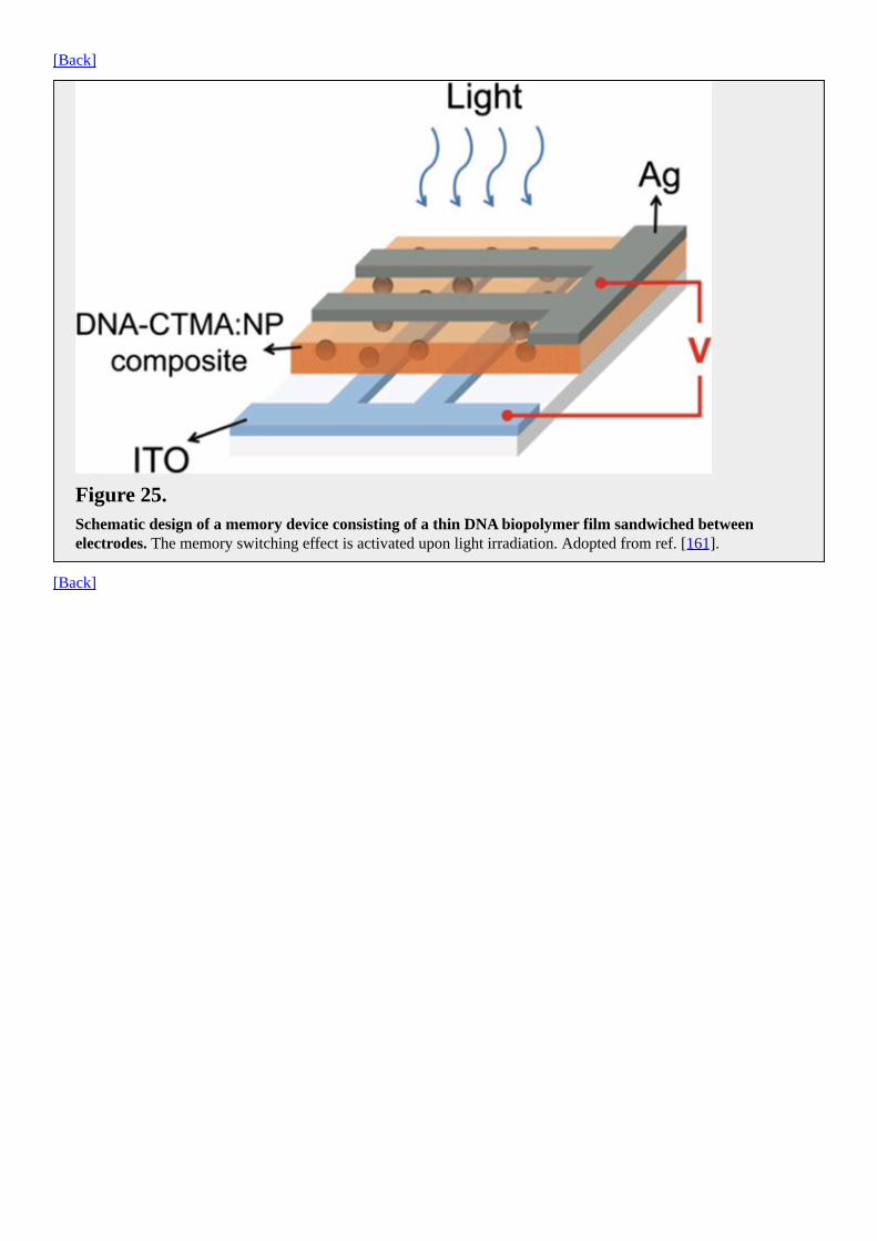
[Back]
Figure25.SchematicdesignofamemorydeviceconsistingofathinDNAbiopolymerfilmsandwichedbetweenelectrodes.Thememoryswitchingeffectisactivateduponlightirradiation.Adoptedfromref.[161].
[Back]

[Back]
Figure26.Structureofquantumdotmemory.Adoptedfromref.[168].
[Back]

[Back]
Figure27.Thebasicdesignofa3-Dcellthatconsistsofaverticaldiodeinseries.(top)Sideview,(bottomright)topview,and(bottomleft)3-Dview.
[Back]

[Back]
Figure28.AschematicdesignofFT-RRAMandaflexible,transparentmemorychipimagecreatedbyresearchersatRiceUniversity.ReproducedfromTourLab/RiceUniversity.
[Back]

[Back]
Figure29.Thebasiccellstructureof1T1R-RRAM.
[Back]


![The Borgias and Their Enemies - DropPDF1.droppdf.com/files/f0jBc/the-borgias-and-their-enemies-christopher... · Orlando, Florida 32887-6777. Library of Congress ... Bride [>] CHAPTER](https://static.documents.pub/doc/80x56/5f67b8d46b1f2812243d4e9c/the-borgias-and-their-enemies-orlando-florida-32887-6777-library-of-congress.jpg)

