Page 1
Fachgebiet 3D-Nanostrukturierung, Institut für Physik
Contact: [email protected] ; [email protected]
Office: Unterpoerlitzer Straße 38 (Heisenbergbau) (tel: 3748) http://www.tu-ilmenau.de/3dnanostrukturierung/
Vorlesung: Wedsnesday 9:00 – 10:30, C 108
Übung: Friday (G), 9:00 – 10:30, C 110
Prof. Yong Lei & Dr. Yang Xu
(a) (b2) (b1)
UTAM-prepared free-standing one-dimensional surface nanostructures on Si
substrates: Ni nanowire arrays (a) and carbon nanotube arrays (b).
Nanostrukturphysik (Nanostructure Physics)
Page 2
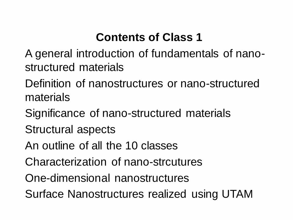
Contents of Class 1
A general introduction of fundamentals of nano-
structured materials
Definition of nanostructures or nano-structured
materials
Significance of nano-structured materials
Structural aspects
An outline of all the 10 classes
Characterization of nano-strcutures
One-dimensional nanostructures
Surface Nanostructures realized using UTAM
Page 3
‘There’s plenty of room at the bottom,
the principles of physics, as far as I can see, do not
speak against the possibility of manoeuvring things atom
by atom...’
By the legendary physicist Richard Feynman in 1959
(Feynman R., Eng Sci, 1960)
Progress made in past two decades has proven this
statement by the amazing nature of nanomaterials, has
achieved exciting technological advancement for the
benefit of mankind.
Page 4
Definition of nanostructures or nano-materials
The word ‘nanometer’ has been assigned to indicate the size of 10-9
meter
Structures with at least one dimension within 1-100 nanometer (nm)
called ‘nanostructures’ (Prof. H. Gleiter 1986-1988)
The word ‘nano’ derived from a Greek word ‘nanos’, means ‘dwarf’
(small)
Nanostructures have received high research interest because of their
peculiar and fascinating properties, as well as their unique applications
superior to their counterparts - bulk materials.
Nowadays, nanomaterials and nanostructures are not only one of the
hottest fundamental research topics, but also gradually intrude into our
daily life.
Page 5
From: J. Henk Introduction to the Theory of Nanostructures (Lecture Notes 2006)
Page 6
Nobel Prizes with research related to nanotechnology:
1986 Physics: G. Binnig, H. Rohrer: design of the scanning
tunneling microscope (STM) → SPM systems;
1996 Chemistry: R. Curl, H. Kroto, R. Smalley: discovery of
fullerenes (C60, bucky balls);
2002 Chemistry: J. Fenn, K. Tanaka, K. Wüthrich: identification
and structure analyses of biological macromolecules;
2003 Chemistry: P. Agre, R. MacKinnon: discoveries of
channels in cell membranes.
2010 Physics: A. Geim, K. Novoselov: for groundbreaking
experiments regarding the two-dimensional graphene
Page 7
G. Binnig (German) & H. Rohrer (Swiss) Nobel Prize 1986 Physics Designing of the scanning tunneling microscope (STM) → SPM systems
Nobel Prizes with research related to nanostructures:
G. Binnig also designed AFM with other 2 scientists, and started the company ‚Definiens‘ in 1994. He worked as honorary professors in some universities, e.g., Uni-Muenchen.
Page 8
8
Konstantin Novoselov & Andre Geim (Russian) Nobel Prize 2010 Physics for groundbreaking experiments regarding the two-dimensional graphene
Page 9
Prof. Andre Geim (from: en.wikipedia.org/wiki/Andre_Geim)
obtained first tenured position in 1994, associate professor at
Uni-Nijmegen, one doctoral student at Nijmegen was Novoselov.
Geim said that he had an unpleasant time during his career in
Netherlands. He was offered professorships at Nijmegen and
Eindhoven, but turned them down as he found the Dutch
academic system too hierarchical and full of politicking. "This can
be pretty unpleasant at times," he says. "It's not like the British
system where every staff member is an equal quantity.“
Geim writes in his Nobel lecture that "the situation was a bit
surreal because outside the university walls I received a warm-
hearted welcome from everyone around……
In 2001 he became a professor at the University of Manchester,
and was appointed director of the Manchester Centre for
Mesoscience and Nanotechnology in 2002.
Page 10
For carbon nanotubes –
CNT (by Ijima in 1991)
and the equally important
discovery of inorganic
fullerene structures (by
Tenne)
1996: Curl, Kroto, Smalley
1985 or1986: fullerenes
(C60, bucky balls);
2010: Geim, Novoselov
2005-2007: 2D graphene
The allotropes of
carbon:
hardest natural
substance, diamond
one of the softest known
substances, graphite.
Allotropes of carbon: a) diamond; b) graphite;
c) lonsdaleite; d–f) fullerenes (C60, C540, C70); g)
amorphous carbon; h) carbon nanotube.
from http://en.wikipedia.org/wiki/Carbon.
Page 11
Graphene is a 1-atom thick sheet of sp2-bonded carbon atoms that are
densely packed in a honeycomb crystal lattice. Graphene is easily
visualized as an atomic-scale wire made of carbon atoms and their bonds.
Graphite consists of many graphene sheets stacked together.
(http://en.wikipedia.org/wiki/Graphene)
Page 12
Zigzag carbon nanotube
Page 13
Armchair carbon nanotube
Page 14
Why are nanostructures interesting?
• small is different: new properties of materials
at nanometer scale
• look at quantum mechanics
• nanostructure + functions or properties:
revolution in information technology, medicine,
media ......
Page 15
Many opportunities might be realized by making new types
of nanostructures (fabrication ways):
1. simply by down-sizing existing microstructures into 1-100
nm range:
most successful example is microelectronics, where
‘smaller‘ means greater performance (since the invention of
integrated circuits): more components per chip, faster
operation, lower cost, and less power consumption;
Page 16
Structural aspects of nano-structured materials:
Extremely large surface area (very large surface/volume ratio):
when the dimensions decrease from micron level to nano level, the
surface area increases by 3 orders in magnitude. This will lead to much
improved and enhanced physical properties (sensing, optical,
catalysis ...):
Cube – Cubic structures – divided into 8 pieces – surface area 2
times(doubled)
Cube – Cubic structures – divided into 1000 pieces – surface area 10
times
Page 17
Many opportunities might be realized by making new types
of nanostructures (fabrication ways):
2. Miniaturization also represent the trend in a range of
other technologies:
Information storage, e.g., many efforts to fabricate magnetic
and optical storage components with critical dimensions
(feature size) as small as tens of nanometer – device
miniaturization
Page 18
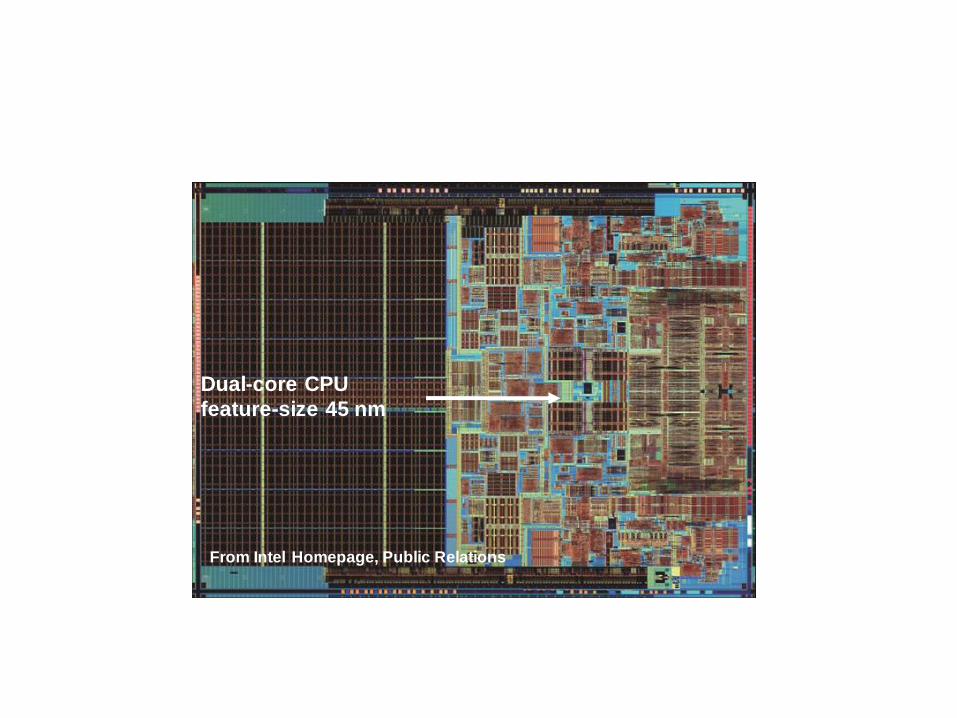
From Intel Homepage, Public Relations
Dual-core CPU
feature-size 45 nm
Page 19
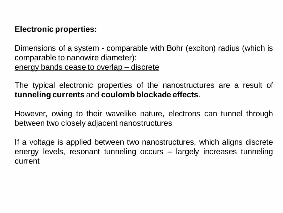
Electronic properties:
Dimensions of a system - comparable with Bohr (exciton) radius (which is
comparable to nanowire diameter):
energy bands cease to overlap – discrete
The typical electronic properties of the nanostructures are a result of
tunneling currents and coulomb blockade effects.
However, owing to their wavelike nature, electrons can tunnel through
between two closely adjacent nanostructures
If a voltage is applied between two nanostructures, which aligns discrete
energy levels, resonant tunneling occurs – largely increases tunneling
current
Page 20
The physical properties of functional nanostructure are different from
those of the bulk materials, especially for optical properties:
Quantum confinement effect (size-reduction down to the nm-sized
range) → a band-gap shift → adjust the optical properties of
nanostructures.
Quantum confinement effect:
It is widely accepted that quantum confinement of electrons by the
potential wells of nanometer-sized structures provides the most
powerful (and versatile) means to control the electrical, optical,
magnetic, and thermoelectric properties of a solid-state materials.
Metallic nanostructures (especially Au and Ag) have unique optical
properties → surface-enhanced plasmon resonance light-scattering
and Raman scattering (SERS or SRR).
Page 21
Quantum confinement effect
When the feature size of a structure (e.g., particle) is comparable
with the size of Bohr (exciton) radius (about 2–50nm, usually below
10-15 nm), electron becomes more confined in particle, quantum
confinement effect lead to an increasing of energy band-gap.
Furthermore, the valence and conductive bands break into
quantized discrete energy levels.
Many exceptional physical properties of nano-materials are attributed to
the changes in the total energy and structure of the system.
Band-gap shift due to the Quantum confinement effect:
ΔEg = h2/8R2μ – 1.8e2 /4πεoεR
Page 22
Quantum confinement in semiconductor nanoparticles
Optical fluorescence of CdSe nanoparticles
of various sizes.
The band gap emission is observed to shift
through the entire visible range, from red emission for the largest particles, to blue
emission for the smallest clusters.
(B. O. Dabbousi, J. Phys. Chem. B, 1997, 101, 9463)
Page 23
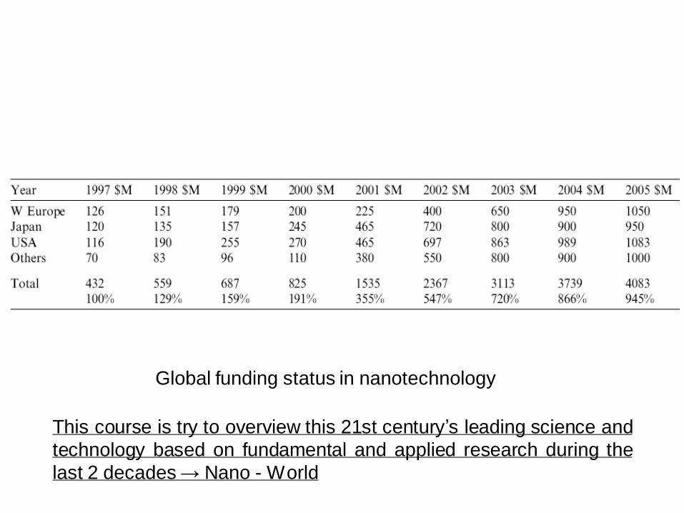
Global funding status in nanotechnology
This course is try to overview this 21st century’s leading science and
technology based on fundamental and applied research during the
last 2 decades → Nano - World
Page 24
Zentralbau des Deutschen Museums
https://de.wikipedia.org/wiki/Deutsches_Museum
Deutsches Museum
Page 25
• Class 1: a general introduction of fundamentals of nano-structured materials, and definition
• Class 2: research at 3D-Nanostructuring
• Class 3: optical properties of 1D nanostructures
• Class 4: carbon nanotubes
• Class 5: graphene
• Class 6: 2D atomically thin nanosheets
• Class 7: lithium-ion batteries: Si nanostructures
• Class 8: solar water splitting I: fundamentals
• Class 9: solar water splitting II: nanostructures for water splitting
• Class 10: solar cells
Page 26
Class 2: research at 3D-Nanostructuring
From template to energy: • Sodium-ion
batteries • Solar water
splitting • Supercapacitors
Page 27
Class 3: optical properties of 1D nanostructures
• Features
• Quantum confinement
• Nanowire lasing
• Field emission display
Page 28
Class 4: carbon nanotubes
• History
• Fabrication
• Applications
Page 29
Class 5: graphene
• Introduction
• Brief history
• Characterizing graphene flakes
• Devices with peeled graphene
• Alternatives to mechanical exfoliation
Page 30
Class 6: atomically thin nanosheets
• Characterization of structure
• Electronic structure regulation
• Energy device construction
Page 31
Class 7: nanostructured Si anodes for lithium-ion batteries
• Principle of lithium-ion batteries
• Opportunities and challenges of Si anodes
• Nanostructured Si anodes
Page 32
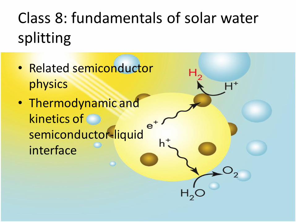
Class 8: fundamentals of solar water splitting
• Related semiconductor physics
• Thermodynamic and kinetics of semiconductor-liquid interface
Page 33
Class 9: nanostructures for solar water splitting
• Pros and cons
• Material designs and nanostrcutured architectures
Anode Cathode Electrolyte
Page 34
Class 10: nanostructures for enhancing light absorption in solar cells
• Semiconductor nanostructures
• Metal nanostructures: surface plasmons
Page 35
Characterization of nano-strcutures
An appropriate characterization will play a crucial role in determining
various structures and properties of nanostructures.
Three broadly approved aspects of characterization are
1. Morphology
2. Crystalline structure
3. Chemical analysis
Page 36
SEM: Scanning Electron Microscopy; STM/AFM: Scanning Tunneling
Microscopy/Atomic Force Microscopy; ATEM: Analytical Transmission
Electron Microscopy
X-Ray: X-ray Morphology; IP: Image Processing; LM: Lightweight
Morphology; RBS: Rutherford Backscattering Spectrometry (Kelsall et al., Nanoscale science and technology. 2005)
Page 37
ATEM: Analytical Transmission Electron Microscopy; AES: Auger
Electron Spectrometer; XRD: X-ray Diffraction; RBS: Rutherford
Backscattering Spectrometry; XPS: X-ray Photoelectron Spectrometer;
(Kelsall et al., Nanoscale science and technology. 2005)
Page 38
SEM: Scanning Electron Microscopy; ATEM: Analytical Transmission
Electron Microscopy;
AEM: Auger Electron Microscopy. XRD: X-ray Diffraction; LEED: Low-
energy electron diffraction; RBS: Rutherford Backscattering
Spectrometry (Kelsall et al., Nanoscale science and technology. 2005)
Page 39
Types of Nanostructure: Two-dimensional nanostructure: nanowalls, quantum wells... One-dimensional nanostructure: nanowires, nanotubes, nanorods, nanobelts... Zero-dimensional nanostructure: quantum dots or nanoparticles
Page 40
Graphene is a 1-atom thick sheets of sp2-bonded carbon atoms that are densely
packed in a honeycomb crystal lattice. Graphene is easily visualized as an atomic-
scale wire made of carbon atoms and their bonds. Graphite consists of many
graphene sheets stacked together.
(http://en.wikipedia.org/wiki/Graphene)
Page 41
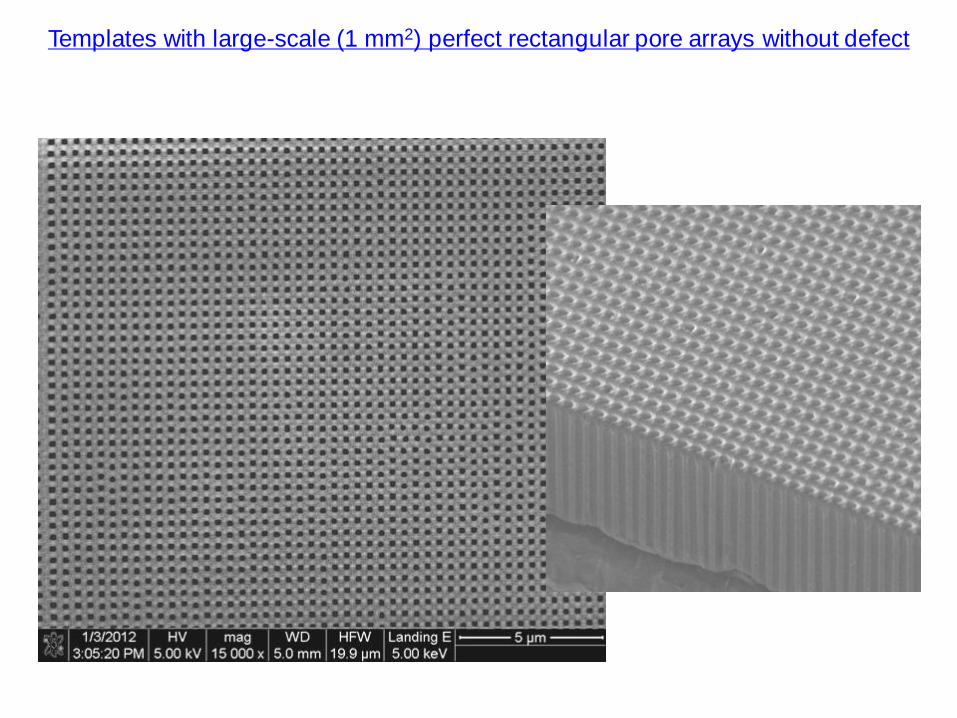
Templates with large-scale (1 mm2) perfect rectangular pore arrays without defect
Page 42
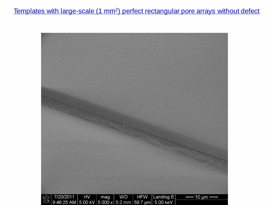
Templates with large-scale (1 mm2) perfect rectangular pore arrays without defect
Page 43
Perfect regular 3D nanostructure arrays with different wire configuration
Page 44
One dimensional nanostructures
One dimensional (1D) nanostructure: nanowires,
nanotubes, nanorods, nanobelts...
One dimensional nanostructure refers to the systems with
the lateral dimension in the range of 1-100 nm.
In comparison with 0D nanostructures, 1D nanostructures
provides a better model system to investigate the
dependence of properties (electronic transport, optical,
and mechanical) on size confinement and dimension.
Nanowires, in particular, plays an important role as both
interconnects and active components in preparing
nanoscale devices (Nano-devices).
Page 45
One-Dimensional Nanostructures
(a) (b2) (b1)
UTAM-prepared free-standing one-dimensional surface nanostructures on Si substrates: Ni
nanowire arrays (a) and carbon nanotube arrays (b). (Y. Lei et al., Chemistry of Materials, 2004)
Page 46
A schematic summary of the kinds of
one dimensional nanostructures already
reported:
(A) nanowires and nanorods;
(B) core–shell structures;
(C) nanotubes/hollow nanorods;
(D) heterostructures;
(E) nanobelts/nanoribbons;
(F) nanotapes;
(G) dendrites;
(H) hierarchical nanostructures;
(I) nanosphere assembly;
(J) nanosprings.
(Kolmakov et al., Annu Rev Mater Res 2004)
Page 47
Highly ordered CdS nanodot arrays, UTAMs and CdS top layer on
the surface of the UTAM.
CdS replicated mask
Alumina
CdS nanodots
Page 48
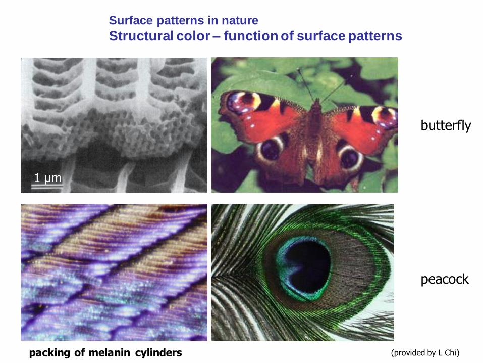
Surface patterns in nature
Structural color – function of surface patterns
1 µm
butterfly
peacock
packing of melanin cylinders (provided by L Chi)
Page 49
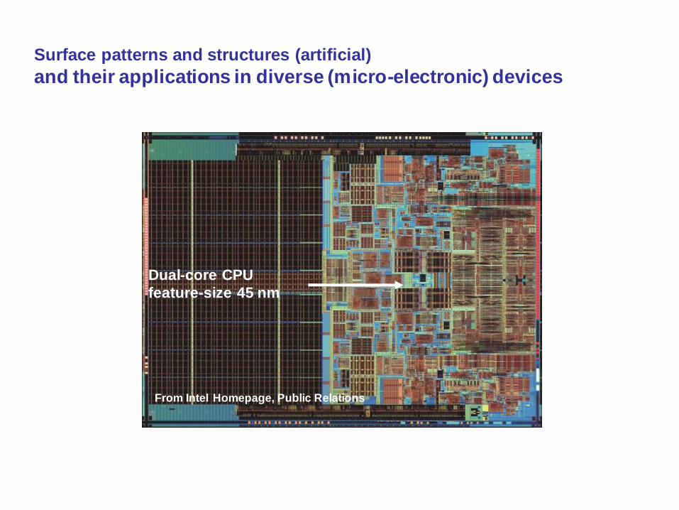
Surface patterns and structures (artificial)
and their applications in diverse (micro-electronic) devices
From Intel Homepage, Public Relations
Dual-core CPU
feature-size 45 nm
Page 50
Surface Nano-Patterning
Fabrication of surface nanostructures
Memory devices with high integration density;
Field emission devices;
Sensors with high sensitivity;
Optical devices with tunable properties
What is an excellent surface nano-patterning technique?
1. Ability to prepare surface patterns within the nanosized range;
2. Well-defined surface nano-patterns;
3. Large pattern area – high throughput;
4. A general process – applicable;
5. Low cost. Perfect ?
Page 51
Electron-beam lithography
Excellent structural controlling Low throughput
High equipment costs
Imprint technologies
High throughput Wear
Structures with low
aspect ratio
Self assembly Low costs
High throughput
Limited class of materials
Low structural controlling
Some surface nano-patterning techniques
in fabricating ordered surface nanostructures
Alternative method that combines these advantages and is applicable
for a broad range of surface nanostructures ?
UTAM (ultra-thin alumina mask) surface nano-patterning:
Template-based surface nano-fabrications
Page 52
Porous Alumina Membranes (PAMs)
Interesting and useful features:
• highly ordered pore arrays +
large area
• Nanometer-sized pores
• High aspect ratio
• size controllable (10 – 400 nm)
Configuration diagram of the PAMs
Page 53
Porous Alumina Membranes (PAMs)
(a) (b)
Regular arrays of short (a) and long Ni nanowires (b) after the removal of PAM, the
diameter is about 90 nm, the length is about 800-1000 nm (a) and 3-4 μm (b), respectively.
thus the aspect ratio of the nanowires are about 10 (a) and 40 (b), respectively.
Page 54
Motivation
Use ultra-thin ordered porous alumina as evaporation or etching masks, and
transfer the regularity of the pore arrays to the nanostructure arrays on
substrates.
UTAM surface nano-patterning technique
Fabrication of Highly Ordered Nanoparticle Arrays Using Ultra-thin
Alumina Mask (UTAM)
Page 55
Fabricating ultra-thin alumina masks (UTAM) on Al foils and then
mounting them onto the surface of silicon wafers
Al foil
First alumina layer
Al foil Al foil
Second alumina layer
Al foil
Ultra-thin alumina mask
Si wafer
Ultra-thin alumina mask
Fabrication process
Page 57
Fabrication of the nanodot arrays
Ultra-thin alumina mask
Si wafer
Ultra-thin alumina mask
Si wafer
Ultra-thin alumina mask Nanoparticle array
Si wafer Si wafer
Page 58
Highly ordered CdS nanodot arrays, UTAMs and CdS top layer on
the surface of the UTAM.
CdS replicated mask
Alumina
CdS nanodots
Page 59
• Class 1: a general introduction of fundamentals of nano-structured materials, and definition
• Class 2: research at 3D-Nanostructuring
• Class 3: optical properties of 1D nanostructures
• Class 4: carbon nanotubes
• Class 5: graphene
• Class 6: 2D atomically thin nanosheets
• Class 7: lithium-ion batteries: Si nanostructures
• Class 8: solar water splitting I: fundamentals
• Class 9: solar water splitting II: nanostructures for water splitting
• Class 10: solar cells
Page 60
Thanks for your attention