+ All Categories
Home > Documents > Nanotechnology Overview - NIST

Nanotechnology Overview - NIST

Date post: 20-Mar-2022
Category:
Upload: others
View: 2 times
Download: 0 times
Share this document with a friend
32
Stanford University Center for Integrated Systems 2005.03.18 Department of Electrical Engineering Nanotechnology Overview H.-S. Philip Wong Professor of Electrical Engineering Stanford University, Stanford, California, U.S.A. [email protected] http://www.stanford.edu/~hspwong
Transcript

Stanford University

Center for Integrated Systems 2005.03.18 Department of Electrical Engineering

Nanotechnology Overview

H.-S. Philip WongProfessor of Electrical Engineering Stanford University, Stanford, California, [email protected]

http://www.stanford.edu/~hspwong

Stanford University

Department of Electrical Engineering2 H.-S. Philip Wong 2005.03.18

Nanoelectronics – Si CMOS

0.001

0.01

0.1

2000 2010 2020

micron

1

10

100

nm

45 nm

65 nm

32 nm

22 nm

16 nm

11 nm

8 nm

Generation

L GATE

Courtesy of Intel Corp.

Stanford University

Department of Electrical Engineering3 H.-S. Philip Wong 2005.03.18

Nanotechnology

A

B1 µm

STM Image

50µ m

light in

2F 2FS

Figures courtesy of IBM Research

Stanford University

Department of Electrical Engineering4 H.-S. Philip Wong 2005.03.18

Nanotechnology

A

B1 µm

STM Image

50µ m

light in

2F 2FS

Figures courtesy of IBM Research

One day, it may replace Si CMOS…

Stanford University

Department of Electrical Engineering5 H.-S. Philip Wong 2005.03.18

Key Challenges

Power / performance improvement and optimization

Variability

Integration– Device, circuit, system

Stanford University

Department of Electrical Engineering6 H.-S. Philip Wong 2005.03.18

Nanotubes and Nanowires

STM Image

Nanotubes

Nanowire

Stanford University

Department of Electrical Engineering7 H.-S. Philip Wong 2005.03.18

Length: several µmDiameter: ~1 nm

20 nm

B.I.Yakobson and R.E.Smalley,American Scientist 85 (1997) 324 S.Iijima, Nature 354 (1991) 56

n,m=(10,10) -- metallic

n,m=(10, 0) -- semiconductingSTM Image

CNT Families and Structure

Stanford University

Department of Electrical Engineering8 H.-S. Philip Wong 2005.03.18

1998 Carbon Nanotube FETsTans et al. Delft UniversityNature 393, 49 (1998)

P-type, high contact resistance

Martel et al. IBMApp. Phys. Lett. 73, 2447 (1998)

P-type, high contact resistance

Stanford University

Department of Electrical Engineering9 H.-S. Philip Wong 2005.03.18

Carbon Nanotube FET

Stanford University

Department of Electrical Engineering10 H.-S. Philip Wong 2005.03.18

Carbon Nanotube FET

Data from:S. Huang et al, IEDM, p. 237, 2001.A. Javey et al., IEDM, p. 741, 2003.

Drain current normalized by gate capacitance

-1.2 -0.8 -0.4 0.0 0.4 0.8 1.20.000.020.040.060.080.100.120.140.160.180.200.220.24

Vg - VT = 1.3, 1.0, 0.7 0.4, 0.1, -0.2V

Vg = 1.2, 1.0, 0.8 0.6, 0.4, 0.2V

Vg = -1.2, -1.0, -0.8 -0.6, -0.4, -0.2V

Vg - VT = -3.3, -2.9, -2.5, -2.1 -1.7, -1.3, -0.9, -0.5 -0.1, +0.3V

Solid line = 2.5/3 µm CNFETDashed line = 50 nm Si FET

Nor

mal

ized

Dra

in C

urre

nt |I

d| / C

[mA-µm

/fF]

Drain Voltage Vd [V]

Stanford University

Department of Electrical Engineering11 H.-S. Philip Wong 2005.03.18

Carbon Nanotube FET is Promising...CV/I, Gmsat/C are comparable to or better than Si nFET

Chemical synthesis controls a key dimension– think of this as an ultra-thin body SOI with body thickness and device width

controlled to atomic precision

Band structure of CNFET:– Symmetric band structure

• electron and hole transport should be identical• balanced nFET and pFET

– Thermal velocity / source injection velocity of CNFET higher than Si FET– However, density of states is lower - lower gate capacitance

Carrier transport is one-dimensional - reduced phase space for scattering

Wrap-around (“double”) gate - thicker gate oxide possible

All bonds are satisfied, stable, and covalent

Device is not “wed” to a particular substrate - 3D plausible

Circuit design infrastructure preserved - no need to reinvent circuits

Stanford University

Department of Electrical Engineering12 H.-S. Philip Wong 2005.03.18

CNFET vs. Si MOSFET

CNTFETs (VDD = 0.4V)

p-CNT MSDFET (projected)

CNT MOSFET (projected)

p-CNT MSDFET (Javey)

Source: M. Lundstrom, IBM Post-CMOS Deep Dive, Sept 21-22, 2004.

Si n-MOS data is 70 nm LG from 130 nm technologyfrom Antoniadis and Nayfeh, MIT

Stanford University

Department of Electrical Engineering13 H.-S. Philip Wong 2005.03.18

Key Issue: Materials and FabricationRight kind of tube (electronic properties) at the right places (placement, orientation), doping

Low parasitic capacitance/resistance, compact device (including isolation) structure

Process compatibility with Si CMOS

catalystsnanotubes nanotubes

D. Singh et al., unpublished (2003)

Stanford University

Department of Electrical Engineering14 H.-S. Philip Wong 2005.03.18

Si Nanowire Growth

Catalyst size controls nanowire size

Y. Cui...C. Lieber et al., Appl. Phys. Lett., 78, p. 2214 (2001)

Stanford University

Department of Electrical Engineering15 H.-S. Philip Wong 2005.03.18

Courtesy of Lars Samuelson, Lund University, 2004.

Nanowires – 3D Heterogeneous Integration Fabric

MOVPE growth of GaAs (core) / AlGaAs (shell) nanowire

AB

A B B

InP/InAs nanowire

Core-shell Axial hetero-epitaxy

Stanford University

Department of Electrical Engineering16 H.-S. Philip Wong 2005.03.18

NanowireNanowire NanotubeNanotube

1D Channel FET:

1D semiconductors (nanotube, nanowire)– Chemical synthesis controls the critical dimension (reduces

variation due to quantum confinement)

– Self-assembly or directed growth – new manufacturing methods

– Nanowire (Si, Ge, III-V, II-VI) is the next logical step after Si FinFET• Bandgap engineering and strain engineering tricks still possible• Both lateral (along axis) and radial (core-shell) engineering possible

– Excess noise for 1D conductors may be problematic – needs study

Stanford University

Department of Electrical Engineering17 H.-S. Philip Wong 2005.03.18

Nanotubes and Nanowires

Net: basic science has progressed to a level where engineering work is feasible

Stanford University

Department of Electrical Engineering18 H.-S. Philip Wong 2005.03.18

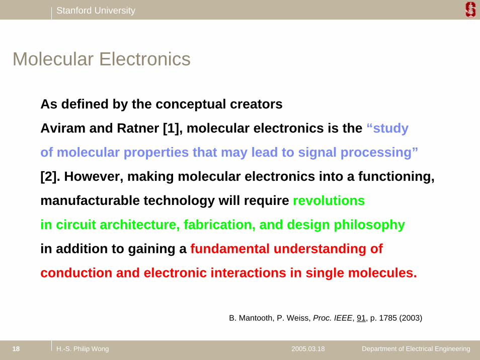
Molecular Electronics

As defined by the conceptual creators

Aviram and Ratner [1], molecular electronics is the “study

of molecular properties that may lead to signal processing”

[2]. However, making molecular electronics into a functioning,

manufacturable technology will require revolutions

in circuit architecture, fabrication, and design philosophy

in addition to gaining a fundamental understanding of

conduction and electronic interactions in single molecules.

B. Mantooth, P. Weiss, Proc. IEEE, 91, p. 1785 (2003)

Stanford University

Department of Electrical Engineering19 H.-S. Philip Wong 2005.03.18

Molecules = Small ?

L >2.5 – 3 nm

All devices are governed by electrostatics and eventually limited by tunneling

- difficult to be much smaller than 2 - 3 nm

Si FET Molecular Device

TSi=7nm Lgate=6nm

Source Drain

Gate

B. Doris et al., IEDM , 2002.

Stanford University

Department of Electrical Engineering20 H.-S. Philip Wong 2005.03.18
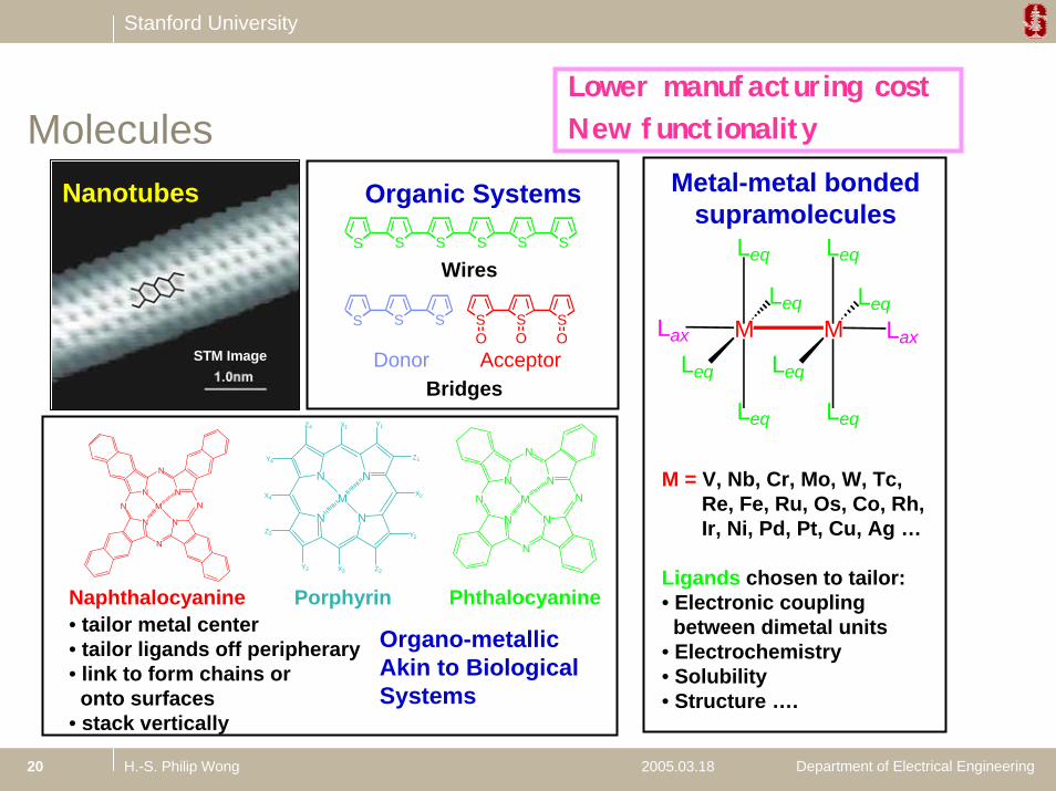
Molecules

Leq

Leq Leq

Leq

MLeq Leq

Leq Leq

M LaxLax

M = V, Nb, Cr, Mo, W, Tc, Re, Fe, Ru, Os, Co, Rh, Ir, Ni, Pd, Pt, Cu, Ag …

Ligands chosen to tailor:• Electronic coupling

between dimetal units• Electrochemistry• Solubility• Structure ….

Metal-metal bondedsupramolecules

Porphyrin

N N

N N

M

X1

X2

X3

X4

Y1

Z1

Z2

Y2

Z4

Y4

Z3

Y3

N

N

N

N

N

N

N

NM

Phthalocyanine

N

N

N

N

N

N

N

NM

Naphthalocyanine• tailor metal center• tailor ligands off peripherary• link to form chains or

onto surfaces• stack vertically

Organo-metallicAkin to Biological Systems

S S S S SS YX

Wires

S S S S SS YX

OOODonor Acceptor

Bridges

Organic Systems

STM Image

Nanotubes

Lower manufacturing costNew functionality

Stanford University

Department of Electrical Engineering21 H.-S. Philip Wong 2005.03.18

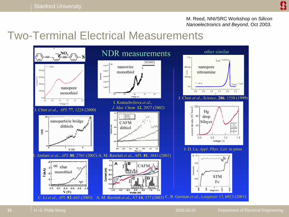
M. Reed, NNI/SRC Workshop on Silicon Nanoelectroincs and Beyond, Oct 2003.

Two-Terminal Electrical Measurements

Stanford University

Department of Electrical Engineering22 H.-S. Philip Wong 2005.03.18

Molecular Memory and ROM-Based Logic

Y. Chen...J.F. Stoddart, R.S. Williams et al., Nanotechnology, 14, p. 462 (2003)

Stanford University

Department of Electrical Engineering23 H.-S. Philip Wong 2005.03.18

Hysteresis – A Dime a Dozen

Stanford University

Department of Electrical Engineering24 H.-S. Philip Wong 2005.03.18
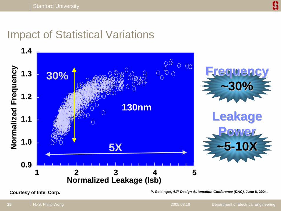
Key Challenges

Power / performance improvement and optimization

Variability

Integration– Device, circuit, system

Nanomaterials

Stanford University

Department of Electrical Engineering25 H.-S. Philip Wong 2005.03.18

Impact of Statistical Variations

130nm

30%

5X0.90.9

1.01.0

1.11.1

1.21.2

1.31.3

1.41.4

11 22 33 44 55Normalized Leakage (Normalized Leakage (IsbIsb))

Nor

mal

ized

Fre

quen

cyN

orm

aliz

ed F

requ

ency FrequencyFrequency

~30%~30%

LeakageLeakagePowerPower~5~5--10X10X

P. Gelsinger, 41st Design Automation Conference (DAC), June 8, 2004.Courtesy of Intel Corp.

Stanford University

Department of Electrical Engineering26 H.-S. Philip Wong 2005.03.18

Can These be Fabricated for 10 nm FET ?

Source: Toshiba,

K. Uchida et al., IEDM 2003

Source: Samsung

J.-H. Yang et al., IEDM 2003

Stanford University

Department of Electrical Engineering27 H.-S. Philip Wong 2005.03.18

Nanomaterials1st pentacenelayer

pentaceneisland

500 nm × 500 nm, VS = -2.0V

50 Å50 Å

1st pentacenelayer

5 nm

10 nm

10 nm

(200)

40 nm

(100)

Co/Ni 9 nm A

60 nm

FePt 4 nmCo 8 nm Ni 9 nm

Courtesy of IBM Research

Stanford University

Department of Electrical Engineering28 H.-S. Philip Wong 2005.03.18

Nano for Si Technology – Nano, Now !

To make these structures

Source: Toshiba,

K. Uchida et al., IEDM 2003

Source: Samsung

J.-H. Yang et al., IEDM 2003

Use techniques that produce these:

Stanford University

Department of Electrical Engineering29 H.-S. Philip Wong 2005.03.18

Lithography Subdivision

Templated assembly of nanostructures

Combines top-down lithography with bottom-up assembly

Provides feature registration with larger, irregular features

2F 2FS

diblock copolymer molecule

PS

PMMA

microphase separation

C. Black et al., IEEE Trans. Nanotechnology, p. 412 (2004).

Stanford University

Department of Electrical Engineering30 H.-S. Philip Wong 2005.03.18

Metrology and Characterization

Cannot manufacture if we cannot measure what we makeWish list– Fast AFM

• The equivalent of the CD SEM – Defect recognition for new materials

• nanotube, nanowire, organic molecules– Defect repair– Characterization methods for soft materials

Stanford University

Department of Electrical Engineering31 H.-S. Philip Wong 2005.03.18

Strained Si, Ge, SiGe, III-V

isolation

buried oxide

Silicon Substrate

Transport-enhanced FET

back-gate

channel

isolation

buried oxide

channel

top-gate

Multi-Gate / FinFET

Source Drain

Gate

Nanowire

3D, heterogeneous integration Nanotube

Molecular devices

Dra

in C

urre

nt (l

og(I D

))

Gate Voltage (VGS)

S < kT/q

A Possible Path

Spintronics

Embedded memory

Quantum cascade

Fine-grain FLA / PLA

Time

Stanford University

Center for Integrated Systems 2005.03.18 Department of Electrical Engineering

Questions? Please contact:

H.-S. Philip WongProfessor of Electrical Engineering Stanford University, Stanford, California, [email protected]

http://www.stanford.edu/~hspwong


Recommended