135

NANOTUBES AND NANOWIRES
SELECTED TOPICS IN ELECTRONICS AND SYSTEMS
Editor-in-Chief: M. S. Shur
Published
Vol. 29: Compound Semiconductor Integrated Circuits ed. Tho T. Vu
Vol. 30: Terahertz Sensing Technology - Vol. 1 Electronic Devices and Advanced Systems Technology eds. D. L. Woolard, W. R. Loerop and M. S. Shur
Vol. 31 : Advanced Device Modeling and Simulation ed. T. Grasser
Vol. 32: Terahertz Sensing Technology - Vol. 2 Emerging Scientific Applications and Novel Device Concepts eds. D. L. Woolard, W. R. LoeropandM. S. Shur
Vol. 33: GaN-Based Materials and Devices eds. M. S. Shurand R. F. Davis
Vol. 34: Radiation Effects and Soft Errors in Integrated Circuits and Electronic Devices eds. R. D. Schrimpf and D. M. Fleetwood
Vol. 35: Proceedings of the 2004 IEEE Lester Eastman Conference on High Performance Devices ed. Robert E. Leoni 111
Vol. 36: Breakdown Phenomena in Semiconductors and Semiconductor Devices M. Levinshtein, J. Kostamovaara and S. Vainshtein
Vol. 37: Radiation Defect Engineering Kozlovski V. and Abrosimova V.
Vol. 38: Design of High-speed Communication Circuits ed. R. Hatjani
Vol. 39: High-speed Optical Transceivers eds. Y. Liu and H. Yang
Vol. 40: Sic Materials and Devices - Vol. 1 eds. M. S. Shur, S. Rumyantsev and M. Levinshtein
Vol. 41 : Frontiers in Electronics Proceedings of the WOFE-04 eds. H Iwai, Y. Nishi, M. S. Shurand H. Wong
Vol. 42: Transformational Science and Technology for the Current and Future Force eds. J. A. Parmentola, A. M. Rajendran, W. Bryzik, B. J. Walker, J. W. McCauley, J. Reifman, and N. M. Nasrabadi
Vol. 43: Sic Materials and Devices - Vol. 2 eds. M. S. Shur, S. Rumyantsev and M. Levinshtein
Selected Topics in Electronics and Systems - Vol. 44
NANOTUBES AND NAN OW I RES
Editor
Peter John Burke University of California, Irvine, USA
World Scientific 1; N E W JERSEY LONDON * SINGAPORE * BElJlNG - S H A N G H A I * HONG KONG * TAIPEI * CHENNAI
Published by
World Scientific Publishing Co. Pte. Ltd. 5 Toh Tuck Link, Singapore 596224 USA office: 27 Warren Street, Suite 401-402, Hackensack, NJ 07601 UK ofice: 57 Shelton Street, Covent Garden, London WC2H 9HE
British Library Cataloguing-in-Publication Data A catalogue record for this book is available from the British Library.
NANOTUBES AND NANOWIRES
Copyright Q 2007 by World Scientific Publishing Co. Pte. Ltd
All rights reserved. This book, or parts thereoj may not be reproduced in any form or by any means, electronic or mechanical, including photocopying, recording or any information storage and retrieval system now known or to be invented, without written permission from the Publisher.
For photocopying of material in this volume, please pay a copying fee through the Copyright Clearance Center, Inc., 222 Rosewood Drive, Danvers, MA 01923, USA. In this case permission to photocopy is not requiredfrom the publisher
ISBN- 13 978-98 1-270-435- 1 ISBN- 10 981 -270-435-3
Editor: Tjan Kwang Wei
Printed in Singapore by Mainland Press
PREFACE
The field of nanotubes and nanowires is evolving at a rapid pace, with many potential applications in electronics, optics, and sensors, to name a few. In this special issue, several groups summarize some of these potential applications, although the list is by no means extensive. Rather, it is meant to serve as a flavor of and snapshot of the current state of the art in the field of nanowires and nanotubes. There is an ample mix of experimental, theoretical, and visionary material in this book to give the reader an indication of where the field is now, and where it is going.
Two chapters on the electrostatics and quantum properties of Id FETs provide a snapshot of the understanding of device physics. One of the chapters focuses on a particular materials system (ZnO) for nanowire technology. Three chapters point to some of the potential applications, including sensors, memory, and high frequency electronics and systems.
While research continues at a rapid pace in academia and industry, the reader will get a good idea of the potential and current state of the art of the field, and will be in a better position to judge for themselves if and when the technology will find commercial applications.
Peter Burke Guest Editor Irvine, California
V

This page intentionally left blankThis page intentionally left blank
CONTENTS
Preface
Nanostructured ZnO: Building Blocks for Nanoscale Devices Z. Fan and J . G. Lu
Carbon Nanotube Field-Effect Transistors J . GUO, S. 0. Koswatta, N. Neophytou and M. Lundstrom
Carbon Nanotube Based Microwave Resonator Gas Sensors M. P. McGrath and A . Pham
Electrostatics of Nanowires and Nanotubes: Application for Field-Effect Devices
A . Shik, H. E. Ruda and S. V. Rotkin
Carbon Nanotube Based Nonvolatile Memory Devices Y. Zhang
Single-Walled Carbon Nanotubes: Applications in High Frequency Electronics
P. J . Burke, C. Rutherglen and Z. Yu
V
1
15
31
55
77
95
vii

This page intentionally left blankThis page intentionally left blank
World Scientific www.worldscientiIic.com
International Journal of High Speed Electronics a n d Systems
@ World Scientific Publishing Company Vol. 16, NO. 4 (2006) 883-896
Nanostructured ZnO: Building Blocks for Nanoscale Devices
Z. FAN AND J. G. LU
Department of Chemical Engineering and Materials Science &
Department of Electrical Engineering and Computer Science University of California, Irvine, CA 92697, USA
ZnO is attracting intensive attention for its versatile applications in transparent electronics, UV emitter, piezoelectric devices, chemical sensor and spin electronics. As one of the direct wide band gap semiconductors, it has advantages over GaN due to its larger exciton binding energy, better lattice match on heteroepitaxial growth and availability of single crystal substrate. Large effort has been invested in the growth of nanostructured ZnO to explore its potentials for nanoscale device applications. ZnO nanobelts, nanowires, nanorings, and nanohelixes demonstrate the diversity of ZnO nanostructures family. This review presents recent research on ZnO nanostructures. Issues of synthesis methods, optical, electrical, gas sensing and magnetic properties are summarized. These progresses constitute the basis for developing future applications in nanoscale electronics, optoelectronics, chemical sensor and spintronics.
Keywords: wide band gap semiconductor; nanostructures; transparent electronics; UV emission; chemical sensor; spintronics
1. Introduction
Zinc oxide (ZnO) is one of the most important functional oxide semiconductors because of its unique properties and potential applications in manifold fields, such as transparent electronics, ultraviolet (UV) light emitter, surface acoustic wave (SAW) devices and spin electronics. Invisible thin film transistors (TFTs) using ZnO as an active channel achieve much higher field effect mobility (7 cmZN.s) than amorphous silicon TFTs (0.5 cm2N.s) [l-31. ZnO has been proposed to be a more promising UV emitting phosphor than GaN because of its large exciton binding energy (60 mew, larger than the thermal energy at room temperature. This lowers the W lasing threshold and yields higher UV emitting efficiency at room temperature [4]. Excitonic emissions have been observed from the photoluminescence spectra of ZnO nanorods [ 5 ] . Large scale vertically aligned ZnO nanorods have been synthesized, demonstrating the potential of fabricating nano-optoelectronics arrays [ 6 ] . SAW filters using ZnO films have already been used for video and radio frequency circuits. Piezoelectric ZnO thin film has been fabricated into ultrasonic transducer arrays operating at 100 MHz [7]. Holes mediated ferromagnetic ordering in bulk ZnO by introducing manganese (Mn) as dopant has been predicted theoretically [8] and reported recently [9]. Vanadium doped n-type ZnO films also demonstrate a Currie temperature above room temperature [ 101. Due to these remarkable
1
884 Z. Fan €4 J . G. Lu
physical properties and the motivation of the device miniaturization trend, large efforts have been focused on nanoscale ZnO materials to fabricate high density, high speed, low power devices. An assortment of ZnO nanostructures, such as nanorods, nanowires, and nanorings, have been successhlly grown via a variety of methods including chemical vapor deposition, thermal evaporation, and electrodeposition [ 11-14]. These nanostructures have been subjected to electrical transport [ 15,161, UV emission [4,17], gas sensing [18], and ferromagnetic doping [9,19,20] studies, and considerable progresses have been achieved. In this paper, recent research achievements on ZnO nanostructures are reviewed, summarizing studies on their synthesis methods, structural, mechanical, electrical, sensing, optical, and magnetic properties.
2. Synthesis and characterization of ZnO nanostructures
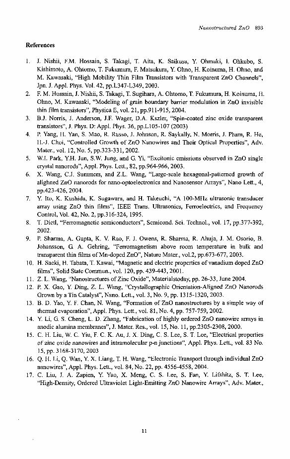
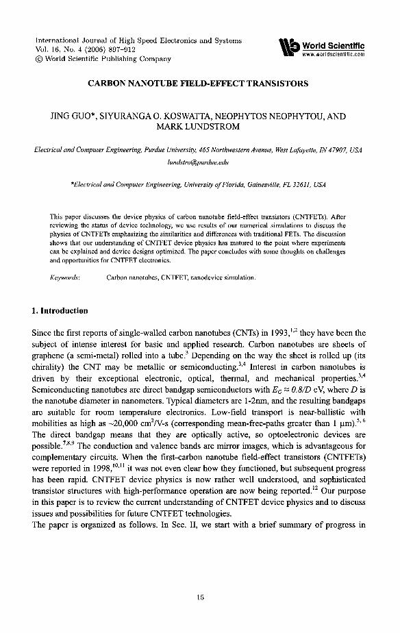
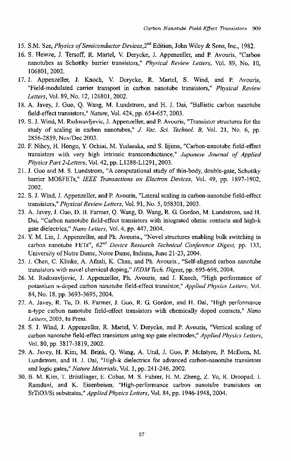
ZnO nanostructures are usually obtained via a vapor transport process. Depending on the synthesis condition variations in temperature, catalyst, and composition of source materials, a wide range of nanostructures has been obtained. Using a vapor-solid process, complex ZnO nanostructures such as nanohelixes, nanorings and nanobelts were synthesized by Kong et al. [21] (Fig. la). In this process, ZnO powder was decomposed into Zn2+ and 0" at -1400 "C then transported by Ar carrier gas to a low temperature zone (-400 "C), and nanostructures were formed on a collecting chip. In a similar vapor transport and condensation process reported by Ren et al. [22, 231, hierarchical ZnO nanostructures were grown by mixing ZnO, In203 and graphite powder and heated up to 820-870 "C. A simplified method to achieve nanowires, nanoribbons and nanorods was reported by Yao et al. [ 131: ZnO powder was mixed with graphite and heated to 1100 "C then cooled down, nanostructures were found to form on the wall of the furnace. These synthesis methods utilize the vapor-solid (VS) mechanism, in which ZnO nanostructures are formed by condensing directly from vapor phase. Although diverse nanostructures can be obtained, this method provides less control on the geometry of ZnO nanostructures. Controlled growth of ZnO nanowires has been achieved by using various nanoparticles or nanoclusters as catalysts, such as Au [24, 251, Cu [26], and Co [27]. In these cases, ZnO and carbon powder are usually used as source material and a vapor-liquid-solid (VLS) growth mechanism governs the synthesis. In the VLS mechanism, the catalyst nanoparticles become liquid droplet under reaction temperature. The reactant Zn vapor generated by carbon thermal reduction of ZnO powder is transported to the catalyst nano-droplets and form Zn-catalyst alloy. In the meantime, ZnO forms as a result of the reaction between Zn and CO/C02. Upon suppersaturation, ZnO nanowires grow from the droplets. Recently we have found that this synthesis process can be further simplified by directly heating pure Zn powder in low concentration oxygen environment (2%) using Au nanoparticles as catalysts [28]. The as-synthesized nanowires show high quality and they grow along (0001) direction, as indicated in Figs. l b & Ic. The advantage of using nanoparticles as catalysts lies in the better control of the nanostructure growth. Based on the VLS mechanism, the diameter of nanowire can be tuned by using different size nanoparticle catalysts. Yang et al. reported achievements of ZnO nanowires growth in controlling the position, orientation, diameter and density [4]. In their method, (110) plane sapphire was used as an epitaxial substrate to obtain vertically grown ZnO nanowires along the (001) direction (Fig. Id). Besides using sapphire as epitaxy substrate, anodic alumina membranes (AAM) was utilized
2
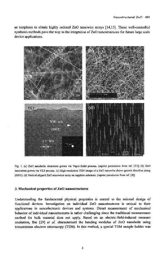
as templates to obtain highly ordered ZnO nanowire arrays [ 14,151. These w e l ~ - c o n ~ ~ l e d synthesis methods pave the way to the integration of ZnO nanoshctures for future large scale device applications.
Pig. 1. (a) ZnO nmohelix structures grown via Vapor-Solid process. (reprint pemission from ref. [all) (b) ZnO nanowires grown via VLS process. {c) High resolution TEM image of a ZnO nanowire shows growth direction along (0001). (d) Vertical aligned ZnO nanowires may on sapphire substrate. (reprint permission from ref. 141)
3. Mechanical properties of ZnO ~ a n o $ t ~ ~ c t ~ ~ e $
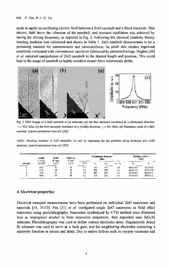
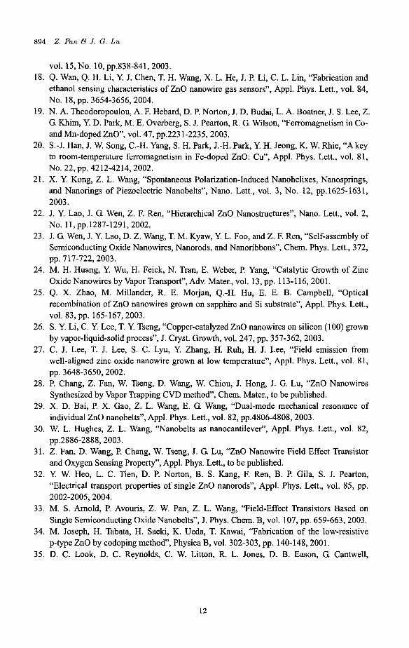
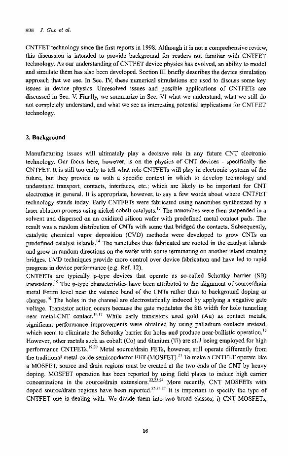
Umders~and~n~ the hdamental physical properties is central to the rational design of functional devices. Investigation on individua~ ZnO nanostructures is critical to their applications in nanoe~ec~onic devices and systerns. Direct m e ~ u ~ m e n t of mechanical behavior of i ~ d i ~ d u a ~ nanoshctures is rather challenging since the traditional measurement method for bulk material does not apply. Based on an eiec~c-~eld-induced resonant excitation, Bai [29] ef al. characterized the bending modulus of ZnO nanobelts using ~ a n s ~ ~ s s ~ o m electron microscopy (TEM). In this method, a special TEM sample holder was
3
886 Z. Fan & J . G. Lu
made to apply an oscillating electric field between a ZnO nanobelt and a fixed electrode. This electric field drove the vibration of the nanobelt, and resonant oscillation was achieved by tuning the driving frequency, as depicted in Fig. 2. Following the classical elasticity theory, bending modulus was calculated and shown in Table 1. ZnO nanobelt demonstrates to be a promising material for nanoresonator and nanocantilever. Its small size renders improved sensitivity compared with conventional cantilever fabricated by microtechnology. Hughes [30] et al. reported manipulation of ZnO nanobelt to the desired length and position. This could lead to the usage of nanobelt as highly sensitive atomic force microscopy probe.
(W (4
ti
229 230 231 232 233 Frequency (KHz)
F L Fig. 2 TEM images of a ZnO nanobelt at (a) stationary (b) the first harmonic resonance in x (thickness) direction, v x= 622 KHz, (c) the first harmonic resonance in y (width) direction, v y= 691 KHz. (d) Resonance peak of a ZnO
nanobelt. (reprint permission from ref. [29])
Tablel. Bending modulus of ZnO nanobelts. Ex and Ey represents for the modulus along thickness and width direction. (reprint permission from ref. [29])
EX ES Na~lobclt ( 2 0 0 5 ) (21) (21) U'<T PXi I.,, " , , V 1 l
I 8 23 55 33 1 7 232 373 1 6 466206 501206 I 4 73 28 19 1 5 396 576 14 4 3 2 1 3 455t29 3 4 07 31 LO 16 662 958 1 4 5 6 3 r 0 9 6 4 6 2 2 3 1 890 45 39 1 1 710 231 1 1 179206 399?12
4. Electrical properties
Electrical transport measurements have been performed on individual ZnO nanowires and nanorods [16, 31-33]. Fan [31] et al. configured single ZnO nanowires as field effect transistors using photolithography. Nanowires synthesized by CVD method were dispersed first in isopropanol alcohol to form nanowires suspension, then deposited onto SiO,/Si substrate. Photolithography was used to define contact electrodes array. Degenerately doped Si substrate was used to serve as a back gate, and the neighboring electrodes contacting a nanowire function as source and drain. Due to native defects such as oxygen vacancies and
4
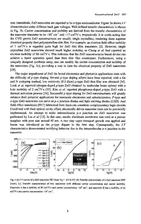
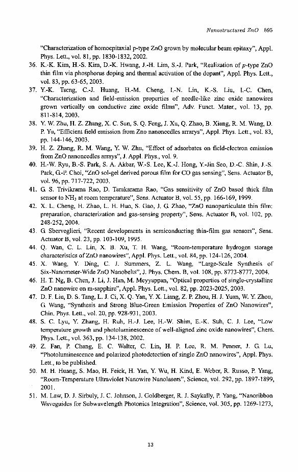
zinc intersti~als, ZnO nanowires are reported to be n-type semiconductor. Figure 3a shows I-V characteristics under different back gate voltages. Well defined transfer characteristic is s h o w in Fig. 3b. Carrier concentration and mobility are derived from the transfer chmcwistic o f the nanowire transistor to be -lo7 cm-' and -1'7 cm2N.s, respectively. I1 is worth noting that the CVI) grown ZnO nanostructures are usually single crystalline, rendering them superior electrical property than polycrystalline thin film. For example, an electron field effkct mobility of 7 cm2N,s is regarded quite high for ZnO thin film transistors [2]. However, single crystalline ZnO nanowires showed much higher mobility, as Chmg et d had reported an electron mobility of 80 cm2N.s. This indicates that the ZnO nanostructures based device can achieve a faster operation speed than their thin film counterpart. F ~ e ~ o r e ~ using a uniquely designed synthesis setup, one can modifj the carrier concentration and mobility of the nanowires (Fig. 3c), providing a way to tune the electrical property of ZnO nanowires
The major impediment of ZnQ for broad electronics and photonics applications rests with the d i ~ c u ~ t y ofp-type doping. Several ptype doping efforts have been reported, with a Ga and W codoping method, low resistivity (0.5 Qcm) p-type ZnO thin film was obtained /34]. Look et 01. reported nitrogen-doped p-type ZnO obtained by molecular beam epitaxy with a hole mobiiity of 2 cm2N.s [35]. Kim ei al. reported phospho~s- dope^ p-type ZnO with a thermal activation process [36]. Successful p-type doping for ZnO n a n o ~ ~ c t ~ ~ s will greatly enhance their potential applications for nanoscale electronics and op~oe~ec~onics. P-type md Pa-type ZnO nanowires can serve as p-n junction diodes and light emitting diodes (LED). And field effect transistors (FET) fabricated from them can constitute c o m ~ l e ~ e ~ t a r y logic circuits. Combined with their optical cavity effect, electrically driven nanowire laser can be potentially ~mpieme~ted. An attempt to make intramolecular p-n junction on ZnQ nanowires was performed by Liu ef srl [15]. In this case, anodic aluminum membrane was used as a porous template with pore size around 40 nm. A two step vapor transport growth was applied and boron was introduced as the p-type dopant in the first step. Consequently, the I-V characteristics demonstrated rectifying behavior due to the i n ~ o l e c u ~ a r p-n junction in the nanowire~
PSI.
a //
Fig. 3 (a) I-Vcurves of a ZnO nanowire FET from Vg = -6V to 4V; (h) Transfer characteristic of a ZnO nanowipe FET (inset); (c) Transfer characteristics of two nanowires with different carrier ~ncentration md carrier mobility. Nanowire A has a mobility of 80 cm2N*s and &er concentration -lo6 em"'; and nanowire B has a mobility of 22
m2N.s and carrier concentration -1 0' cm-'.
5
888 Z. Fan 6Y J. G. LU
5. Electron field emission from vertical aligned Zno nanQ~tru~ures
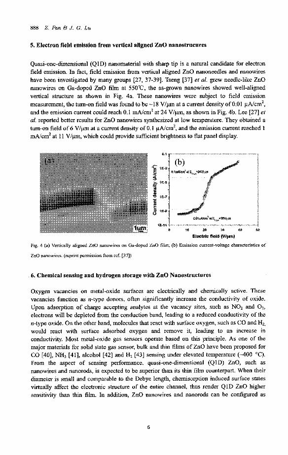
~asi"one"dimensional (Q1 D) nanomaterial with sharp tip is a natural candidate for electron field emission. In fact, field emission fpom vertical aligned ZnO nanoneedles and nanowires have been investigated by many groups [27, 37-39]. Tseng [37] et al. grew needle-like ZnCB n ~ o w i r e s on Ga-doped ZnO film at 550%, the as-grown nanowires showed well-aligned vertical structure as shown in Fig. 4a. These nanowires were subject to field emission m e ~ s ~ ~ ~ e n t , the tm-on field was found to be -18 V/pm at a cwent density of 0.01 pLNcm2, and the emission current could reach 0.1 &em2 at 24 V / w , as shown in Fig. 4b. Lee [27J ef al. reported better results for ZnO nanowires synthesized at low temperature. They obtained a turn-on field o f 6 Vlpm at a current density of 0.1 pNcm2, and the emission current reached 1 &cm2 at 11 Vlpm, which could provide sufficient brightness to flat panel display.
Fig. 4 (a) Vertically aligned ZnO nanowires on Ga-doped ZOO film; (b) Emission current-voltage characteristics o f
ZnO nanowires. (reprint permission from ref. [37])
6. Chemical sensing and hydrogen storage with ZnO Nanostructures
Oxygen vacancies on metal-oxide surfaces are electrically and chemically active. These vacancies function as n-type donors, ofien significantly increase the conductivity of oxide. Upon adsorption of charge accepting analytes at the vacancy sites, such as NO2 and 0 2 ,
electrons will be depleted from the conduction band, leading to a reduced conductivity of the n-type oxide. CBn the other hand, molecules that react with surface oxygen, such as CO and H2,
would react with surface adsorbed oxygen and remove it, leading to an increase in conductivity. Most metal-oxide gas sensors operate based on this principle. As one of the major materials for solid state gas sensor, bulk and thin films of ZnO have been proposed for 60 [40], NH3 1411, alcohol [42] and H2 [43] sensing under elevated temperature (-400 "C). From the aspect of sensing performance, quasi-one-dimensional (QlD) ZnO, such as nanowires and nanorods, is expected to be superior than its thin film counterpart. When their diameter is small and comparable to the Debye length, chemisorption induced surface states virtually affect the electronic structure of the entire channel, thus render Q1D ZnO higher sensitivity than thin film. In addition, ZnO nanowires and nanorods can be configured as
Nanostructured ZnO 889
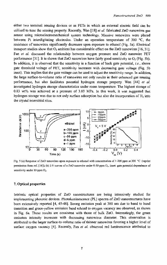
either two terminal sensing devices or as FETs in which an external electric field can be utilized to tune the sensing property. Recently, Wan [ 181 et al. fabricated ZnO nanowires gas sensor using microelectromechanical system technology. Massive nanowires were placed between Pt interdigitating electrodes. Under an operation temperature of 300 "C, the resistance of nanowires significantly decreases upon exposure to ethanol (Fig. 5a). Electrical transport studies show that O2 ambient has considerable effect on the ZnO nanowires [ 16,311. Fan et al. discussed the relationship between oxygen pressure and ZnO nanowire FET performance [31]. It is shown that ZnO nanowires have fairly good sensitivity to 0 2 (Fig. 5b). In addition, it is observed that the sensitivity is a function of back gate potential, i.e., above gate threshold voltage of FET, sensitivity increases with decreasing gate voltage (Fig. 5b inset). This implies that the gate voltage can be used to adjust the sensitivity range. In addition, the large surface-to-volume ratio of nanowires not only results in their enhanced gas sensing performance, but also facilitates potential hydrogen storage property. Wan [44] et al. investigated hydrogen storage characteristics under room temperature. The highest storage of 0.83 wt% was achieved at a pressure of 3.03 MPa. In this work, it was suggested that hydrogen storage was due to not only surface adsorption but also the incorporation of H2 into the crystal interstitial sites.
I 000
100
-0.4 -0.2 0.0 0.2 0.4 10
Fig. 5 (a) Response of ZnO nanowires upon exposure to ethanol with concentration of 1-200 ppm at 300 "C (reprint
permission from ref. [16]); (b) I-V curves of a ZnO nanowire under 0-50 ppm 02. Inset: gate potential dependence of sensitivity under 10 ppm 02.
7. Optical properties
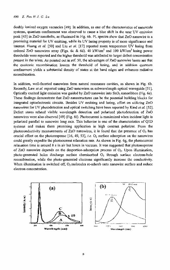
Intrinsic optical properties of ZnO nanostructures are being intensively studied for implementing photonic devices. Photoluminescence (PL) spectra of ZnO nanostructures have been extensively reported [4, 45-48]. Strong emission peak at 380 nm due to band to band transition and green-yellow emission band related to oxygen vacancy are observed, as shown in Fig. 6a. These results are consistent with those of bulk ZnO. Interestingly, the green emission intensity increases with decreasing nanowires diameter. This observation is attributed to the larger surface-to-volume ratio of thinner nanowires favoring a higher level of surface oxygen vacancy [4]. Recently, Fan et al. observed red luminescence attributed to
7
890 2. Fan tY J . G. Lu
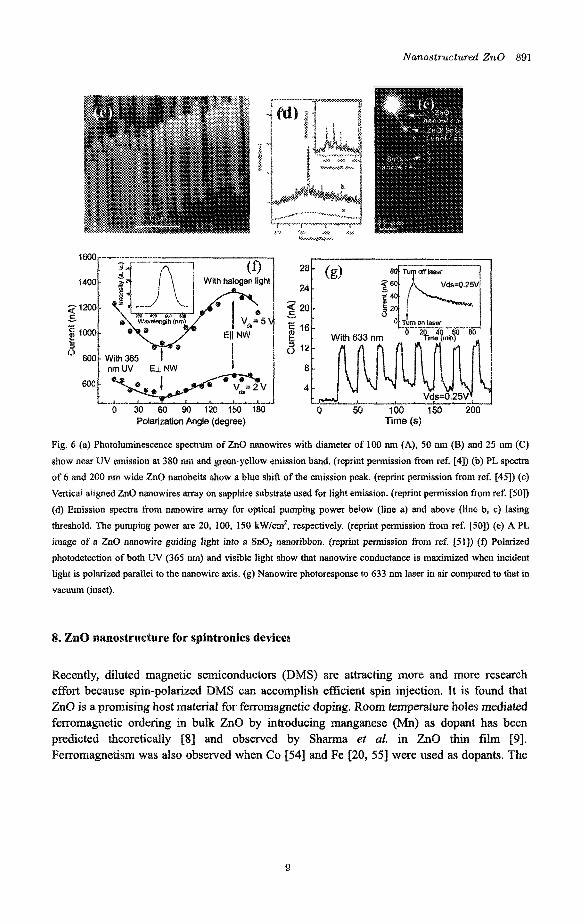
doubly ionized oxygen vacancies [49]. In addition, as one of the characteristics of nanoscale systems, quantum confinement was observed to cause a blue shift in the near UV emission peak [45] in ZnO nanobelts, as illustrated in Fig. 6b. PL spectra show that ZnO nanowire is a promising material for UV emitting, while its UV lasing property is of more significance and interest. Huang et al. [50] and Liu et al. [17] reported room temperature UV lasing from ordered ZnO nanowires array (Figs. 6c & 6d). 40 kW/cm2 and 100 kwlcm'lasing power thresholds were reported and the higher threshold was attributed to larger defect concentration present in the wires. As pointed out in ref. 50, the advantages of ZnO nanowire lasers are that the excitonic recombination lowers the threshold of lasing, and in addition quantum confinement yields a substantial density of states at the band edges and enhances radiative recombination.
In addition, well-facetted nanowires form natural resonance cavities, as shown in Fig. 6b. Recently, Law et al. reported using ZnO nanowires as subwavelength optical waveguide [51]. Optically excited light emission was guided by ZnO nanowire into Sn02 nanoribbon (Fig. 6e). These findings demonstrate that ZnO nanostructures can be the potential building blocks for integrated optoelectronic circuits. Besides UV emitting and lasing, effort on utilizing ZnO nanowires for UV photodetection and optical switching have been reported by Kind et al. [52]. Defect states related visible wavelength detection and polarized photodetection of ZnO nanowires were also observed [49] (Fig. 60. Photocurrent is maximized when incident light is polarized parallel to nanowire long axis. This behavior is one of the characteristics of Q1D systems and makes them promising application in high contrast polarizer. From the photoconductivity measurements of ZnO nanowires, it is found that the presence of 0 2 has crucial effect on the photoresponse [16, 49, 531, i.e. O2 surface adsorption on the nanowires could greatly expedite the photocurrent relaxation rate. As shown in Fig. 6g, the photocurrent relaxation time is around 8 s in air but hours in vacuum. It was suggested that photoresponse of ZnO nanowire depends on the desportion-adsorption process of 02. Upon illumination, photo-generated holes discharge surface chemisorbed 0 2 through surface electron-hole recombination, while the photo-generated electrons significantly increase the conductivity. When illumination is switched off, O2 molecules re-adsorb onto nanowire surface and reduce electron concentration.
8
600
0 30 60 90 120 150 180
28
24
20
16
12
8
4
0 50 100 150 200 Polarization Angle (degree) Time (8)
Fig. 6 (a) Photoluminesc~ce spectrum of ZnO nanowires with diameter of 100 nm (A), 50 nm (B) and 25 nm (C) show near WV emission at 380 nm and green-yellow emission band. (reprint permission from ref. [4]) (b) PL spectra of 6 and 200 nm wide ZnO nanobelts show a blue shift of the emission peak. (reprint permission from ref. [45]) (c)
Vtrtcal aligned ZnO nanowirw array on sapphire substrate wed for light emission. (reprint permission from ref. [sol) (d) Emission spectra Erom nanowire army for optical pumping power below (line a) and above (line h, c) lasing threshofd. The pumping power are 20, 100, 150 kWlcm’, respectively. (reprint permission from ref. [SO]) (e) A PL image of a ZnO nanowire guiding light into a SnOz nanoribbon. (%print permission from ref. [Jl I) If) Polarized photodetection of both UV (365 nm) and visible light show that nanowire conductance is maximized when incident light is polarized piuallei to the nanowke axis. (g) Nanowire photoresponse to 633 nm laser in air compared to that in vacuum (inset).
Recently, diluted magnetic s e ~ i c o n d u c t o ~ (DMS) are attracting more and more research effort because spin-polarized BMS can accomplish efficient spin injection. It is found that ZnO is a promising host material for ferromagnetic doping. Room temperature holes mediated ferromagnetic ordering in bulk ZnO by introducing manganese (Mn) as dopant has been predicted theoretically [S] and observed by S h m a et QZ. in ZnO thin film [9]. ~ e ~ o ~ i a ~ ~ ~ s r n was also observed when Go [54] and Fe [20, 551 were used as dopants. The
9
8.ZnOnanost ructure for sp in t r in ics dev ices
892 Z . Fan €4 J . G. LU
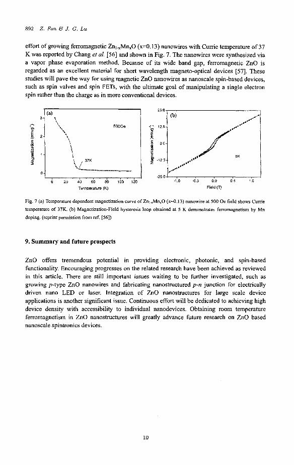
effort of growing ferromagnetic Znl.,Mn,O (x=O. 13) nanowires with Currie temperature of 37 K was reported by Chang et al. [56] and shown in Fig. 7. The nanowires were synthesized via a vapor phase evaporation method. Because of its wide band gap, ferromagnetic ZnO is regarded as an excellent material for short wavelength magneto-optical devices [57]. These studies will pave the way for using magnetic ZnO nanowires as nanoscale spin-based devices, such as spin valves and spin FETs, with the ultimate goal of manipulating a single electron spin rather than the charge as in more conventional devices.
\, / 37u Q.*- ........ n ...... ,....... *-.
i - - r - . i . I ' I ' . - I
0 20 40 60 80 100 120
Temperature (K)
25.0 ,
Field (T)
Fig. 7 (a) Temperature dependent magnetization curve of Zn,..Mn,O (x=O.13) nanowire at 500 Oe field shows Currie
temperature of 37K. (b) Magnetization-Field hysteresis loop obtained at 5 K demonstrates ferromagnetism by Mn
doping. (reprint permission from ref. [56])
9. Summary and future prospects
ZnO offers tremendous potential in providing electronic, photonic, and spin-based functionality. Encouraging progresses on the related research have been achieved as reviewed in this article. There are still important issues waiting to be further investigated, such as growing p-type ZnO nanowires and fabricating nanostructured p-n junction for electrically driven nano LED or laser. Integration of ZnO nanostructures for large scale device applications is another significant issue. Continuous effort will be dedicated to achieving high device density with accessibility to individual nanodevices. Obtaining room temperature ferromagnetism in ZnO nanostructures will greatly advance future research on ZnO based nanoscale spintronics devices.
10
Nanostructured ZnO 893
References
1.
2.
3.
4.
5.
6.
7.
8.
9.
10
11 12
13
J. Nishii, F.M. Hossain, S. Takagi, T. Aita, K. Saikusa, Y. Ohmaki, I. Ohkubo, S. Kishimoto, A. Ohtomo, T. Fukumura, F. Matsukura, Y. Ohno, H. Koinuma, H. Ohno, and M. Kawasaki, “High Mobility Thin Film Transistors with Transparent ZnO Channels”, Jpn. J. Appl. Phys. Vol. 42, pp.L347-L349,2003. F. M. Hossain, J. Nishii, S. Takagi, T. Sugihara, A. Ohtomo, T. Fukumura, H. Koinuma, H. Ohno, M. Kawasaki, “Modeling of grain boundary barrier modulation in ZnO invisible thin film transistors”, Physica E, vol. 21, pp.911-915,2004. B.J. Norris, J. Anderson, J.F. Wager, D.A. Kszler, “Spin-coated zinc oxide transparent transistors”, J. Phys. D: Appl. Phys. 36, pp.Ll05-107 (2003) P. Yang, H. Yan, S. Mao, R. Russo, J. Johnson, R. Saykally, N. Morris, J. Pham, R. He, H.-J. Choi, “Controlled Growth of ZnO Nanowires and Their Optical Properties”, Adv. Mater., vol. 12, No. 5, pp.323-331, 2002. W.I. Park, Y.H. Jun, S.W. Jung, and G. Yi, “Excitonic emissions observed in ZnO single crystal nanorods”, Appl. Phys. Lett., 82, pp.964-966,2003. X. Wang, C.J. Summers, and Z.L. Wang, “Large-scale hexagonal-patterned growth of alighned ZnO nanorods for nano-optoelectronics and Nanosensor Arrays”, Nan0 Lett., 4,
Y. Ito, K. Kushida, K. Sugawara, and H. Takeuchi, “A 100-MHz ultrasonic transducer array using ZnO thin films”, IEEE Trans. Ultrasonics, Ferroelectrics, and Frequency Control, Vol. 42, No. 2, pp.316-324, 1995. T. Dietl, “Ferromagnetic semiconductors”, Semicond. Sci. Technol., vol. 17, pp.377-392, 2002. P. Sharma, A. Gupta, K. V. Rao, F. J. Owens, R. Sharma, R. Ahuja, J. M. Osorio, B. Johansson, G. A. Gehring, “Ferromagnetism above room temperature in bulk and transparent thin films of Mn-doped ZnO”, Nature Mater., v01.2, pp.673-677, 2003. H. Saeki, H. Tabata, T. Kawai, “Magnetic and electric properties of vanadium doped ZnO films”, Solid State Commun., vol. 120, pp. 439-443,2001. Z. L. Wang, “Nanosh-uctures of Zinc Oxide”, Materialstoday, pp. 26-33, June 2004. P. X. Gao, Y Ding, Z. L. Wang, “Crystallographic Orientation-Aligned ZnO Nanorods Grown by aTin Catalyst”, Nano. Lett., vol. 3, No. 9, pp. 1315-1320,2003. B. D. Yao, Y. F. Chan, N. Wang, “Formation of ZnO nanostructures by a simple way of thermal evaporation”, Appl. Phys. Lett., vol. 81, No. 4, pp. 757-759,2002.
pp.423-426,2004.
14. Y. Li, G. S. Cheng, L. D. Zhang, “Fabrication of highly ordered ZnO nanowire arrays in anodic alumina membranes”, J. Mater. Res., vol. 15, No. 11, pp.2305-2308,2000.
15. C. H. Liu, W. C. Yiu, F. C. K. Au, J. X. Ding, C. S. Lee, S. T. Lee, “Electrical properties of zinc oxide nanowires and intramolecular p-n junctions”, Appl. Phys. Lett., vol. 83 No.
16. Q. H. Li, Q. Wan, Y. X. Liang, T. H. Wang, “Electronic Transport through individual ZnO nanowires”, Appl. Phys. Lett., vol. 84, No. 22, pp. 4556-4558,2004.
17. C. Liu, J. A. Zapien, Y. Yao, X. Meng, C. S. Lee, S. Fan, Y. Lifshitz, S. T. Lee, “High-Density, Ordered Ultraviolet Light-Emitting ZnO Nanowire Arrays”, Adv. Mater.,
15, pp. 3168-3170,2003
11
894 2. Fan €4 J . G. Lu
V O ~ . 15, NO. 10, pp.838-841, 2003. 18. Q. Wan, Q. H. Li, Y. J. Chen, T. H. Wang, X. L. He, J. P. Li, C. L. Lin, “Fabrication and
ethanol sensing characteristics of ZnO nanowire gas sensors”, Appl. Phys. Lett., vol. 84,
19. N. A. Theodoropoulou, A. F. Hebard, D. P. Norton, J. D. Budai, L. A. Boatner, J. S. Lee, Z. G. Khim, Y. D. Park, M. E. Overberg, S. J. Pearton, R. G Wilson, “Ferromagnetism in Co- and Mn-doped ZnO”, vol. 47, pp.2231-2235,2003.
20. S.-J. Han, J. W. Song, C.-H. Yang, S. H. Park, J.-H. Park, Y. H. Jeong, K. W. Rhie, “A key to room-temperature ferromagnetism in Fe-doped ZnO: Cu”, Appl. Phys. Lett., vol. 81,
2 1. X. Y. Kong, Z. L. Wang, “Spontaneous Polarization-Induced Nanohelixes, Nanosprings, and Nanorings of Piezoelectric Nanobelts”, Nano. Lett., vol. 3, No. 12, pp.1625-1631, 2003.
22. J. Y. Lao, J. G. Wen, Z. F. Ren, “Hierarchical ZnO Nanostructures”, Nano. Lett., vol. 2,
23. J. G. Wen, J. Y. Lao, D. Z. Wang, T. M. Kyaw, Y. L. Foo, and 2. F. Ren, “Self-assembly of Semiconducting Oxide Nanowires, Nanorods, and Nanoribbons”, Chem. Phys. Lett., 372,
24. M. H. Huang, Y. Wu, H. Feick, N. Tran, E. Weber, P. Yang, “Catalytic Growth of Zinc Oxide Nanowires by Vapor Transport”, Adv. Mater., vol. 13, pp. 113-116,2001.
25. Q. X. Zhao, M. Millander, R. E. Morjan, Q.-H. Hu, E. E. B. Campbell, “Optical recombination of ZnO nanowires grown on sapphire and Si substrate”, Appl. Phys. Lett.,
26. S. Y. Li, C. Y. Lee, T. Y. Tseng, “Copper-catalyzed ZnO nanowires on silicon (100) grown by vapor-liquid-solid process”, J. Cryst. Growth, vol. 247, pp. 357-362,2003.
27. C. J. Lee, T. J. Lee, S. C. Lyu, Y. Zhang, H. Ruh, H. J. Lee, “Field emission from well-aligned zinc oxide nanowire grown at low temperature”, Appl. Phys. Lett., vol. 81,
28. P. Chang, Z. Fan, W. Tseng, D. Wang, W. Chiou, J. Hong, J. G. Lu, “ZnO Nanowires
29. X. D. Bai, P. X. Gao, Z. L. Wang, E. G. Wang, “Dual-mode mechanical resonance of
30. W. L. Hughes, Z. L. Wang, ‘Wanobelts as nanocantilever”, Appl. Phys. Lett., vol. 82,
31. Z. Fan, D. Wang, P. Chang, W. Tseng, J. G. Lu, “ZnO Nanowire Field Effect Transistor and Oxygen Sensing Property”, Appl. Phys. Lett., to be published.
32. Y. W. Heo, L. C. Tien, D. P. Norton, B. S. Kang, F. Ren, B. P. Gila, S. J. Pearton, “Electrical transport properties of single ZnO nanorods”, Appl. Phys. Lett., vol. 85, pp.
33. M. S. Arnold, P. Avouris, Z. W. Pan, Z. L. Wang, “Field-Effect Transistors Based on Single Semiconducting Oxide Nanobelts”, J. Phys. Chem. B, vol. 107, pp. 659-663,2003.
34. M. Joseph, H. Tabata, H. Saeki, K. Ueda, T. Kawai, “Fabrication of the low-resistive p-type ZnO by codoping method”, Physica B, vol. 302-303, pp, 140-148,2001.
35. D. C. Look, D. C. Reynolds, C. W. Litton, R. L. Jones, D. B. Eason, G Cantwell,
NO. 18, pp. 3654-3656,2004.
NO. 22, pp. 4212-4214,2002.
NO. 11, pp.1287-1291,2002.
pp. 717-722,2003.
V O ~ . 83, pp. 165-167,2003.
pp. 3648-3650,2002.
Synthesized by Vapor Trapping CVD method”, Chem. Mater., to be published.
individual ZnO nanobelts”, Appl. Phys. Lett., vol. 82, pp.4806-4808,2003.
pp.2886-2888,2003.
2002-2005,2004.
12
Nanostructured ZnO 895
“Characterization of homoepitaxial p-type ZnO grown by molecular beam epitaxy”, Appl. Phys. Lett., vol. 81, pp. 1830-1 832,2002.
36. K.-K. Kim, H.-S. Kim, D.-K. Hwang, J.-H. Lim, S.-J. Park, “Realization ofp-type ZnO thin film via phosphorus doping and thermal activation of the dopant”, Appl. Phys. Lett.,
37. Y.-K. Tseng, C.-J. Huang, H.-M. Cheng, I.-N. Lin, K.-S. Liu, I.-C. Chen, “Characterization and field-emission properties of needle-like zinc oxide nanowires grown vertically on conductive zinc oxide films”, Adv. Funct. Mater., vol. 13, pp.
38. Y. W. Zhu, H. Z. Zhang, X. C. Sun, S. Q. Feng, J. Xu, Q. Zhao, B. Xiang, R. M. Wang, D. P. Yu, “Efficient field emission from Zno nanoneedles arrarys”, Appl. Phys. Lett., vol. 83,
39. H. Z. Zhang, R. M. Wang, Y. W. Zhu, “Effect of adsorbates on field-electron emission from ZnO nanoneedles arrays”, J. Appl. Phys., vol. 9.
40. H.-W. Ryu, B.-S. Park, S. A. Akbar, W.-S. Lee, K.-J. Hong, Y.-Jin Seo, D.-C. Shin, J.-S. Park, G.-P. Choi, “ZnO sol-gel derived porous film for CO gas sensing”, Sens. Actuator B,
41. G S. Trivikrama Rao, D. Tarakarama Rao, “Gas sensitivity of ZnO based thick film sensor to NH3 at room temperature”, Sens. Actuator B, vol. 55, pp. 166-169, 1999.
42. X. L. Cheng, H. Zhao, L. H. Huo, S. Gao, J. G. Zhao, “ZnO nanoparticulate thin film: preparation, characterization and gas-sensing property”, Sens. Actuator B, vol. 102, pp.
43. G Sberveglieri, “Recent developments in semiconducting thin-film gas sensors”, Sens. Actuator B, vol. 23, pp. 103-109, 1995.
44. Q. Wan, C. L. Lin, X. B. Xu, T. H. Wang, “Room-temperature hydrogen storage characteristics of ZnO nanowires”, Appl. Phys. Lett., vol. 84, pp. 124-126,2004,
45. X. Wang, Y. Ding, C . J. Summers, Z. L. Wang, “Large-Scale Synthesis of Six-Nanometer-Wide ZnO Nanobelts”, J. Phys. Chem. B, vol. 108, pp. 8773-8777,2004.
46. H. T. Ng, B. Chen, J. Li, J. Han, M. Meyyappan, “Optical properties of single-crystalline ZnO nanowire on m-sapphire”, Appl. Phys. Lett., vol. 82, pp. 2023-2025,2003.
47. D. F. Liu, D. S. Tang, L. J. Ci, X. Q. Yan, Y. X. Liang, Z. P. Zhou, H. J. Yuan, W. Y. Zhou, G Wang, “Synthesis and Strong Blue-Green Emission Properties of ZnO Nanowires”, Chin. Phys. Lett., vol. 20, pp. 928-931,2003.
48. S. C. Lyu, Y. Zhang, H. Ruh, H.-J. Lee, H.-W. Shim, E.-K. Suh, C. J. Lee, “Low temperature growth and photoluminescence of well-aligned zinc oxide nanowires”, Chem. Phys. Lett., vol. 363, pp. 134-138,2002.
49. Z. Fan, P. Chang, E. C. Walter, C. Lin, H. P. Lee, R. M. Penner, J. G. Lu, “Photoluminescence and polarized photodetection of single ZnO nanowires”, Appl. Phys. Lett., to be published.
50. M. H. Huang, S. Mao, H. Feick, H. Yan, Y. Wu, H. Kind, E. Weber, R. Russo, P. Yang, “Room-Temperature Ultraviolet Nanowire Nanolasers”, Science, vol. 292, pp. 1897-1 899, 2001.
51. M. Law, D. J. Sirbuly, J. C. Johnson, J. Goldberger, R. J. Saykally, P. Yang, “Nanoribbon Waveguides for Subwavelength Photonics Integration”, Science, vol. 305, pp. 1269-1273,
V O ~ . 83, pp. 63-65,2003.
811-814,2003.
pp. 144-146,2003.
VOI. 96, pp. 717-722,2003.
248-252,2004.
13
896 Z. Fan €9 J . G. Lu
2004. 52. H. Kind, H. Yan, B. Messer, M. Law, P. Yang, “Nanowire Ultraviolet Photodetection and
Optical Switches”, Adv. Mater., vol. 14, pp. 158-160,2002. 53. K. Keem, H. Kim, G.-T. Kim, J. S. Lee, B. Min, K. Cho, M.-Y. Sung, S. Kim,
“Photocurrent in ZnO nanowires grown from Au electrodes”, Appl. Phys. Lett., vol. 84,
54. K. Rode, A. Anane, R. Mattana, J.-P. Contour,“Magnetic semiconductors based on cobalt substituted ZnO”, J. Appl. Phys., vol. 93, pp. 7676-7678,2003,
55. Y. M. Cho, W. K. Choo, H. Kim, D. Kim, Y. Ihm,“Effect of rapid thermal annealing on the ferromagnetic properties of sputtered Znl.,(Coo.SFeo.S),O thin films”, Appl. Phys. Lett.,
56. Y. Q. Chang, D. B. Wang, X. H. Luo, X. Y. Xu, X. H. Chen, L. Li, C. P. Chen, R. M. Wang, J. Xu, D. P. Yu, “Synthesis, optical, and magnetic properties of diluted magnetic semiconductor Znl.,Mn,O nanowires via vapor phase growth”, Appl. Phys. Lett., vol. 83
57. K. Ando, H. Saito, Z. Jin, T. Fukumura, M. Kawasaki, Y. Matsumoto, H. Koinuma, “Large magneto-optical effect in an oxide diluted magnetic semiconductor Znl.xCoxO’, Appl. Phys. Lett., vol. 78 pp. 2700-2702,2001.
pp. 4376-4378,2004.
V O ~ . 80, pp. 3358-3360,2002.
pp. 4020-4022,2003.
14
World Scientific www.worldscient i f ic .com
International Journal of High Speed Electronics a n d Systems
@ World Scientific Publishing Company Vol. 16, NO. 4 (2006) 897-912
CARBON NANOTUBE FIELD-EFFECT TRANSISTORS
JING GUO*, SIYURANGA 0. KOSWATTA, NEOPHYTOS NEOPHYTOU, AND MARK LUNDSTROM
Electrical and Computer Engineering, Purdue University. 465 Northwestern Avenue, West Lafqette, IN 47907, USA
lundstro@purdue. edu
*Electrical and Computer Engineering, Universiry of Florida, Gainesville, FL 32611, USA
This paper discusses the device physics of carbon nanotube field-effect transistors (CNTFETs). After reviewing the status of device technology, we use results of our numerical simulations to discuss the physics of CNTFETs emphasizing the similarities and differences with traditional FETs. The discussion shows that our understanding of CNTFET device physics has matured to the point where experiments can be explained and device designs optimized. The paper concludes with some thoughts on challenges and opportunities for CNTFET electronics.
Keywords: Carbon nanotubes, CNTFET, nanodevice simulation.
1. Introduction
Since the first reports of single-walled carbon nanotubes (CNTs) in 1993,Is2 they have been the subject of intense interest for basic and applied research. Carbon nanotubes are sheets of graphene (a semi-metal) rolled into a tube.3 Depending on the way the sheet is rolled up (its chirality) the CNT may be metallic or semic~nduct ing.~~~ Interest in carbon nanotubes is driven by their exceptional electronic, optical, thermal, and mechanical properties.3p4 Semiconducting nanotubes are direct bandgap semiconductors with EG =: 0.8/D eV, where D is the nanotube diameter in nanometers. Typical diameters are 1-2nm, and the resulting bandgaps are suitable for room temperature electronics. Low-field transport is near-ballistic with mobilities as high as -20,000 cmZN-s (corresponding mean-free-paths greater than 1 ~ ( m ) . ~ ’ The direct bandgap means that they are optically active, so optoelectronic devices are possible.73899 The conduction and valence bands are mirror images, which is advantageous for complementary circuits. When the first-carbon nanotube field-effect transistors (CNTFETs) were reported in 1998,’0v” it was not even clear how they functioned, but subsequent progress has been rapid. CNTFET device physics is now rather well understood, and sophisticated transistor structures with high-performance operation are now being reported.” Our purpose in this paper is to review the current understanding of CNTFET device physics and to discuss issues and possibilities for future CNTFET technologies. The paper is organized as follows. In Sec. 11, we start with a brief summary of progress in
15
898 J . Guo et al.
CNTFET technology since the first reports in 1998. Although it is not a comprehensive review, this discussion is intended to provide background for readers not familiar with CNTFET technology. As our understanding of CNTFET device physics has evolved, an ability to model and simulate them has also been developed. Section I11 briefly describes the device simulation approach that we use. In Sec. IV, these numerical simulations are used to discuss some key issues in device physics. Unresolved issues and possible applications of CNTFETs are discussed in Sec. V. Finally, we summarize in Sec. VI what we understand, what we still do not completely understand, and what we see as interesting potential applications for CNTFET technology.
2. Background
Manufacturing issues will ultimately play a decisive role in any hture CNT electronic technology. Our focus here, however, is on the physics of CNT devices - specifically the CNTFET. It is still too early to tell what role CNTFETs will play in electronic systems of the future, but they provide us with a specific context in which to develop technology and understand transport, contacts, interfaces, etc.; which are likely to be important for CNT electronics in general. It is appropriate, however, to say a few words about where CNTFET technology stands today. Early CNTFETs were fabricated using nanotubes synthesized by a laser ablation process using nickel-cobalt ~ata1ysts.l~ The nanotubes were then suspended in a solvent and dispersed on an oxidized silicon wafer with predefined metal contact pads. The result was a random distribution of CNTs with some that bridged the contacts. Subsequently, catalytic chemical vapor deposition (CVD) methods were developed to grow CNTs on predefined catalyst i~1ands.I~ The nanotubes thus fabricated are rooted in the catalyst islands and grow in random directions on the wafer with some terminating on another island creating bridges. CVD techniques provide more control over device fabrication and have led to rapid progress in device performance (e.g. Ref. 12). CNTFETs are typically p-type devices that operate as so-called Schottky barrier (SB) transistor^.'^ The p-type characteristics have been attributed to the alignment of sourceldrain metal Fermi level near the valance band of the CNTs rather than to background doping or charges.I6 The holes in the channel are electrostatically induced by applying a negative gate voltage. Transistor action occurs because the gate modulates the SB width for hole tunneling near metal-CNT While early transistors used gold (Au) as contact metals, significant performance improvements were obtained by using palladium contacts instead, which seem to eliminate the Schottky barrier for holes and produce near-ballistic operation.I8 However, other metals such as cobalt (Co) and titanium (Ti) are still being employed for high performance CNTFETs. I9,’’ Metal sourceldrain FETs, however, still operate differently from the traditional metal-oxide-semiconductor FET (MOSFET).” To make a CNTFET operate like a MOSFET, source and drain regions must be created at the two ends of the CNT by heavy doping. MOSFET operation has been reported by using field plates to induce high carrier concentrations in the sourceldrain extension^.^^^^^^^^ More recently, CNT MOSFETs with doped sourceldrain regions have been reported.25p26927 It is important to specify the type of CNTFET one is dealing with. We divide them into two broad classes; i) CNT MOSFETs,
16
Carbon Nanotube Field-Efiect Transistors 899
which are analogous to the traditional silicon MOSFET, and ii) CNT MSDFETs, for metal sourceldrain FETs. When the Schottky barrier is large, the MSDFET operates as a classic SBFET, and when the SB is small or absent, they operate somewhere between the limits of a MOSFET and SBFET.” Early CNTFETs were fabricated on oxidized silicon substrates with a back-gated geometry and a thick SiOa layer that resulted in poor gate control of drain The use of a top-gated geometry produced immediate performance improvements.’* Wind et al. deposited a thin dielectric layer (15-20 nm) on top of CNTs, and lithographically defined metal electrodes for gating and contacts. A transconductance (gm = dIdJdV,,Iyds) of 3.25 pS and subthreshold swing (S = ln(l0) [dVg/d@n(IdJ)]) of 130 mV1decade were obtained, which was a significant improvement in device performance?’ Later, the incorporation of high-lc dielectrics in a top-gated structure produced even better device characteristic^.'^ Javey et al. employed a high-lc Zr02 (K - 25) gate dielectric with a thickness of - 8 nm and obtained g, =: 12 pS and S =: 70 mvlde~ade.’~ Although not always with top-gated geometry, other groups have also reported the use of high-lc dielectrics such as HfQ (K - l l ) , TiOz (K - 40-90), SrTi03 (K - 175), and even-electrolyte gating mechanisms for attaining improved p e r f o r m a n ~ e s . ” ~ ~ ~ , ~ ~ ~ ~ ~ , ~ ~ In the case of electrolyte gating, Siddon et al. have reported S =: 62 mV1decade which is very close to the theoretical limit of 60 mvlde~ade.~’ All of these devices appear to operate as CNT MSDFETs, some with essentially no barrier and others with rather large (half bandgap) barriers. The possibility of ballistic operation of CNTFETs has been a topic of great interest. Since there are no dangling bonds in CNTs, surface scattering can be expected to be negligible. Back-scattering by acoustic phonons is suppressed by symmetry arguments related to the CNT b a n d ~ t r u c t u r e ~ ~ , ~ ~ and by the reduction in phase space for one-dimensional conductors. The result is that mean-free-paths of several hundred nanometers are commonly o b ~ e r v e d . ~ ~ * ~ ~ Under high bias, however, optical or zone boundary phonons may be emitted, and the mfps decrease substantially. Yao et al. showed that for long metallic CNTs, the current saturates at about 25 PA per n a n ~ t u b e . ~ ~ They showed that the high-field current is limited by the emission of optical or zone boundary phonons with hwo = 200 meV and that the high-field mfp is - 10nm. Yao’s results suggest that for short nanotubes, comparable in length to the mfp, the current should exceed 25 PA per nanotube. This expectation was confirmed by Park et a1 36
and Javey et al,35 who both showed that the current increases above 25 pA when the length of the nanotube is less than several mfps long. By analyzing their data, both Park and Javey extracted an mfp of -10 - 15 nm, which was consistent with the value extracted by Yao for long nanotubes. The mfps deduced from these experiments are considerably shorter than the values of 50nm or so, which are estimated from the expected electron-phonon coupling strength.33736 Although these results are for metallic nanotubes, similar effects are expected for semiconducting nanotubes and CNTFETs. For a tube much shorter than the mfp, carrier transport in the tube is quasi-ballistic, and the tube resistance is nearly length-independent. In contrast, a tube much longer than the mfp behaves like a classical resistor, in the sense that the resistance is proportional to the tube length. Several recent improvements to CNTFET design collectively incorporate various techniques that have been developed during the past few years. For instance, Javey et al. reported a self-aligned top gate structure that uses the catalytic CVD method for CNT growth, a thin
17
900 J . Guo et al.
HfOz top gate dielectric - 50 nm in length and self-aligned palladium sourceldrain contacts.I2 A transconductance of 30 pS, subthreshold swing of 110 mvldecade, and a saturation current of -25 pA at a power supply of VDD-IV were obtained.I2 Novel CNTFET device structures that enable high current operation 37 and high integration densities 38 have also been reported. These devices are all of the metal source/drain (MSDFET) variety, but it is recognized that the use of a metal source will limit the drain current (unless the SB is sufficiently negative).21 Very recently, CNT MOSFETs with doped sourceldrain regions have been r e p ~ r t e d . ~ ~ - ~ ~ Substitutional doping is not practical because of the strong carbon-carbon bond, so charge transfer approaches analogous to modulation doping in 111-V heterostructures 26327739 are used. Although progress in CNTFETs has been rapid, there are still many issues to address. The potential for digital logic 40,41 was demonstrated early on. Techniques that modify the behavior of the nanotube from p-type to n-type have been implemented, which allowed their use in complementary CMOS logic. Following this, Derycke et al. demonstrated an inverter structure based on nanotubes:' Other nanotube based elementary digital logic gates with high gain and high ZoJZo~ ratios, such as a NOR gate, a ring oscillator and an SRAM cell, have also been im~lemented.~' With respect to RF performance, measurements 42-44 and modeling 45-47 have both been initiated to assess performance potential. Experimental work includes that of Frank and Appen~eller;~,~~ who developed a technique to circumvent the low-current-drive problem of CNTFETs to place a lower bound on the frequency response. Li et al.44 measured the microwave reflection coefficient from a load comprised of a nanotube and a matching circuit and demonstrated transistor operation at 2.6 GHz. In terms of modeling, Burke 45,46 has suggested an RF circuit model for a metallic nanotube, and emphasized the importance of both quantum capacitance and kinetic inductance. More re~ently?~ Burke used a standard formula, along with estimated and measured values for the parameters, to predict the unity-current-gain frequency V;) of CNTFETs, and suggested the fT would be given by 80 GHz divided by the tube length in microns VT = 80 GHz /L(in ,urn)]. However, as we discuss near the end of this paper, much more needs to be done to definitively characterize the RF behavior of CNTFETs. A pressing issue that limits logic and RF device performance has to do with contacts. Good contacts to the valence band are achieved by using palladium. The barrier height is approximately zero for relatively large diameter nanotubes (D - 1.7 nm). Achieving small barrier contacts to the small diameter nanotubes that will be necessary for room temperature operation (D - lnm) is a key challenge, as is also achieving good, low barrier, contacts to the conduction band. CNT MOSFETs, however, are expected to deliver significantly better performance than MSDFETs, and recent progress on stable, heavy doping of CNTs is encouraging.25s26927 For many (perhaps most) applications, high currents are needed, so innovative structures that place several CNTs in parallel will be required. If these problems can be addressed, manufacturing challenges will move to the forefront. The key challenges are control of chirality and development of low temperature growth processes to allow CNTFETs to be placed at low cost on CMOS substrates. For the remainder of this paper, our focus will be on the physics of CNTFETs. Before we examine device physics, we first describe the simulation techniques that we use to explore and understand device physics.
18
Carbon Nanotube Field-Effect Transistors 901
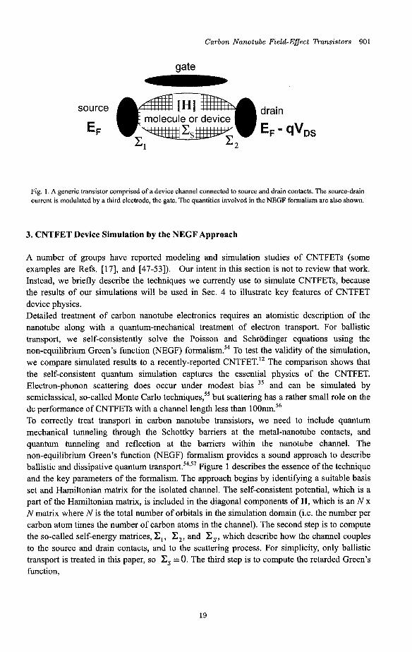
gate
source
EF drain
EF qvDS
Fig. 1. A generic transistor comprised of a device channel connected to source and drain contacts. The source-drain current is modulated by a third electrode, the gate. The quantities involved in the NEGF formalism are also shown.
3. CNTFET Device Simulation by the NEGF Approach
A number of groups have reported modeling and simulation studies of CNTFETs (some examples are Refs. [17], and [47-531). Our intent in this section is not to review that work. Instead, we briefly describe the techniques we currently use to simulate CNTFETs, because the results of our simulations will be used in Sec. 4 to illustrate key features of CNTFET device physics. Detailed treatment of carbon nanotube electronics requires an atomistic description of the nanotube along with a quantum-mechanical treatment of electron transport. For ballistic transport, we self-consistently solve the Poisson and Schrodinger equations using the non-equilibrium Green’s function (NEGF) formalism.s4 To test the validity of the simulation, we compare simulated results to a recently-reported CNTFET.” The comparison shows that the self-consistent quantum simulation captures the essential physics of the CNTFET. Electron-phonon scattering does occur under modest bias 35 and can be simulated by semiclassical, so-called Monte Carlo technique^:^ but scattering has a rather small role on the dc performance of CNTFETs with a channel length less than 100nm.56 To correctly treat transport in carbon nanotube transistors, we need to include quantum mechanical tunneling through the Schottky barriers at the metal-nanotube contacts, and quantum tunneling and reflection at the barriers within the nanotube channel. The non-equilibrium Green’s function (NEGF) formalism provides a sound approach to describe ballistic and dissipative quantum transport.s49s7 Figure 1 describes the essence of the technique and the key parameters of the formalism. The approach begins by identifying a suitable basis set and Hamiltonian matrix for the isolated channel. The self-consistent potential, which is a part of the Hamiltonian matrix, is included in the diagonal components of H, which is an N x N matrix where N is the total number of orbitals in the simulation domain (i.e. the number per carbon atom times the number of carbon atoms in the channel). The second step is to compute the so-called self-energy matrices, z,, Z2, and Z,, which describe how the channel couples to the source and drain contacts, and to the scattering process. For simplicity, only ballistic transport is treated in this paper, so zs = 0. The third step is to compute the retarded Green’s function,
19
902 J . Guo et ol.
Fig. 2. The computed local density of states for a CNTFET under high gate and drain bias. Light areas indicate a high density of states.
The fourtft. step is to determine the physical quantities of interest from the N x N Green’s function matrix. For example, the position-resolved electron density in the device is
whereh.2 the equilibrium Fenni functions of the two contacts, and .LDOS,,2 is the local density of states fillable by contact 1 or contact 2, which are obtained from the retarded Greem’s functiom [eqm. (l)]. For a self-consistent solution, the NEGF tramsport equation is solved iteratively with the Poisson equation until self-consistency is achieved. After that the s o ~ c e ~ ~ a ~ current is computed from
where T ( E ) = Trace(]r ,Gr,G+) is the transmission between the source and the drain,
= i (x , , 2 - Z:,, ) , and the extra factor of two in (3) comes from the valley degeneracy in
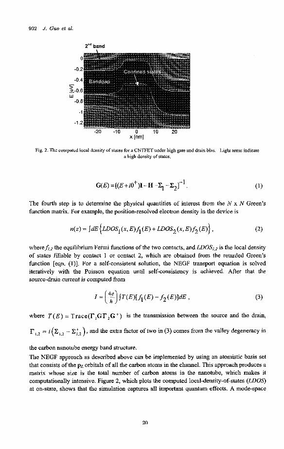
the carbon nanokbe energy band structure. The NEGF approach as described above can be implemented by using an atomistic basis set that consists of the pz orbitals of all the carbon atoms in the channel. This approach produces a matrix whose size is the total number of carbon atoms in the nanotube, which makes it computationally intensive. Figure 2, which plots the computed ~oca~~dens i~of-s ta~es (LDkps) at on-state, shows that the simulation captures all important quantum effects. A mode-space
20
Carbon Nanotzlbe Field-Effect llvLnsistors 903
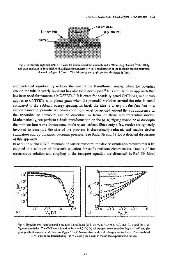
Fig. 3. A recently reported CNTFET with Pd source and drain contacts and a 5Onm-long cha~meI.2~ The Hfoz top-gate insulator is 8ni-n thick with a dielectric constant K = 16. The diameter of the intrinsic carbon nanotube
c h m e l is & = 1.7 nm. The Pd sonrce and drain contact thickness is 7nm.
approach that s~gni~can~ly reduces the size of the Hamiltonian matrix when the potential around the tube is nearly invariant has also been developed.56 It is similar to an approach that has been used for nanoscale MOSFETS.~* It is exact for coaxially gated CNWETs, and it also applies to CNTFETs with planar gates when the potential variation around the tube is small compared to the subband energy spacing. In brief, the idea is to exploit the fact that in a carbon nanotube, periodic boundary conditions must be applied around the circumference of the nanotube, so taansport can be described in terms of these circumferential modes. Ma~emat~ca~ly, we perform a basis transforma~~on on the (n, 0) zigzag nanotube to decouplle the problem into II one~~mens~onal mode-space lattices. Since only a few modes are typically ianvolved in trmsport, the size of the problem is dramatically reduced, and routine device simulation and op t i~za~ ion becomes possible. See Refs. 56 and 59 for a detailed discussion of ahis approach. In addition to the N E W treatment of carrier transport, the device simulation requires that it be coupbd to a solution of Poisson's equation for self-consistent electrostatics. Details of the e%ectrostabic solution and coupling to the transport equation are discussed in Ref. 59. Most
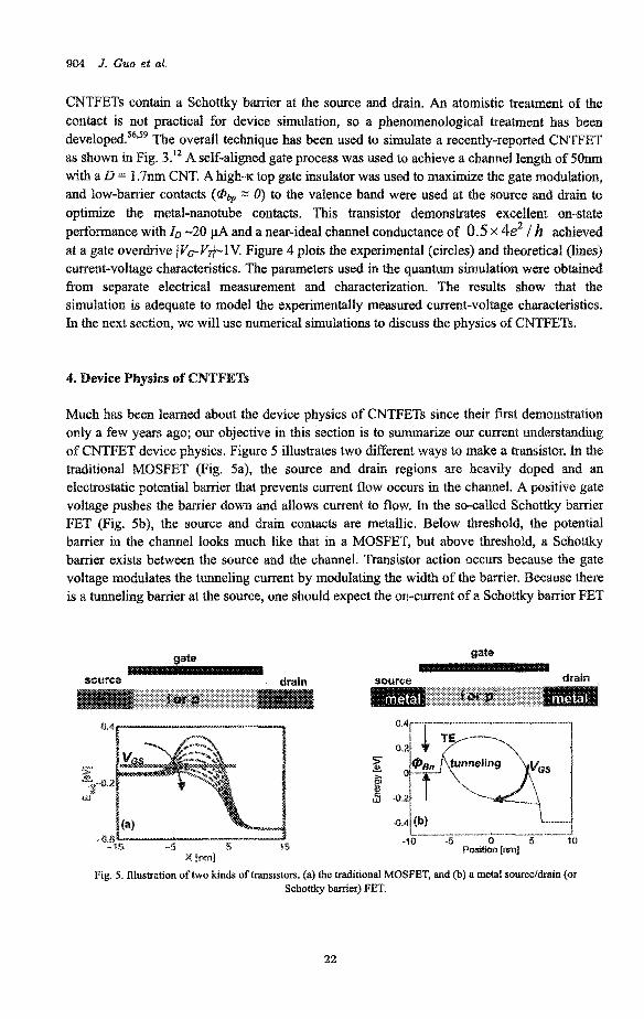
Fig. 4. Experimental (circles) and simulated (solid lines) (a) ID vs. VO at V~=-0.l , -0.2, and -0.3V and @) ID vs. VD characteristics. The CNT work function QCNT = 4.7 cV, the Al topgate work function QAl = 4.1 eV, and the p' doped bottom-gate work function Qfli = 5. I eV. No interface and oxide charges are included. The simulated
ID-VO C M N ~ S are translated by +O. 7.W along the x-axis to match the experimental c w w .
21
904 J . GUO et sk,
CNTFETs contain a Schottky barrier at the source and drain. An atomistic treatment of the contact is not practical for device simulation, so a phenomenological treatment has been d e v e l ~ p e d . ~ ~ ’ ~ ~ The overall technique has been used to simulate a recently-reported CNTFET as shown in Fig. 3.” A self-aligned gate process was used to achieve a channel length o f 56)m with a B = 1.7m CNT. A high-K top gate insulator was used to maximize the gate modulation, and low-bmier contacts (CP, = 0) to the valence band were used at the source and drain to optimize &e metal~nano~be contacts. This transistor demonstrates excellent on-state performance with ID -26) pA and a near-ideal channel conductance of 0.5 X k2 / h achieved at a gate overdrive J V&- kjl-l V. Figwe 4 plots the experimental (circles) and theoretical (lines) current-vo~tage characteristics. The parameters used in the quantum simulation were obtained from separate electrical measurement and characterization. The results show that the simulation is adequate to model the experimentally measured current-voltage characteristics. In the next section, we will use numerical simulations to discuss the physics of CWFETs.
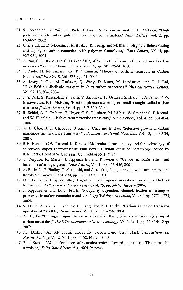
4. Device Physics of CNTFETs
Much has been learned about the device physics of CNTFETs since their first demonstration only a few years ago; our objective in this section is to summarize our current understand~n~ o f CNTFET device physics. Figure 5 illustrates two different ways to make a transistor. In the traditional MOSFET (Fig. 5a), the source and drain regions are heavily doped and an electrostatic potential barrier that prevents current flow occurs in the channel. A positive gate voltage pushes the barrier down and allows current to Row. In the so-called Schottky bmier FET (Fig. %), the source and drain contacts are metallic. Below threshold, the potential barrier in the channel looks much like that in a MOSFET, but above threshold, a Schottky barrier exists between the source and the channel. Transistor action occurs because the gate voltage modulates the tunneling current by modulating the width of the barrier. Because there i s a ling barrier at the source, one should expect the on-current o f a Schottky barrier FET
Fig. 9. Illustration of two kinds of transistors. (a) the traditional MOSFET, and (b) a metal source/drain (or Schottky barrier) FET.
22
Carbon Nanotube Field-Effect Tk-ansistors 905
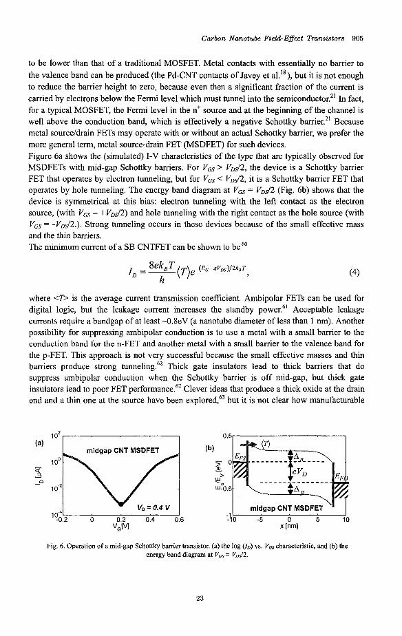
to be lower than that of a traditional MOSFET. Metal contacts with essentially no barrier to the valence band can be produced (the Pd-CNT contacts of Javey et a1.I8), but it is not enough to reduce the barrier height to zero, because even then a significant fraction of the current is carried by electrons below the Fermi level which must tunnel into the semiconductor.21 In fact, for a typical MOSFET, the Fermi level in the n' source and at the beginning of the channel is well above the conduction band, which is effectively a negative Schottky barrier.21 Because metal source/drain FETs may operate with or without an actual Schottky barrier, we prefer the more general term, metal source-drain FET (MSDFET) for such devices. Figure 6a shows the (simulated) I-V characteristics of the type that are typically observed for MSDFETs with mid-gap Schottky barriers. For VGS > vDs/2, the device is a Schottky barrier FET that operates by electron tunneling, but for Vcs < VD&, it is a Schottky barrier FET that operates by hole tunneling. The energy band diagram at VcS = vDs/2 (Fig. 6b) shows that the device is symmetrical at this bias: electron tunneling with the left contact as the electron source, (with VGs = +vDs/2) and hole tunneling with the right contact as the hole source (with VGS = -V&2.). Strong tunneling occurs in these devices because of the small effective mass and the thin barriers. The minimum current of a SB CNTFET can be shown to be 6o
where <T> is the average current transmission coefficient. Ambipolar FETs can be used for digital logic, but the leakage current increases the standby power.61 Acceptable leakage currents require a bandgap of at least -0.8eV (a nanotube diameter of less than 1 nm). Another possibility for suppressing ambipolar conduction is to use a metal with a small barrier to the conduction band for the n-FET and another metal with a small barrier to the valence band for the p-FET. This approach is not very successful because the small effective masses and thin barriers produce strong tunneling.62 Thick gate insulators lead to thick barriers that do suppress ambipolar conduction when the Schottky barrier is off mid-gap, but thick gate insulators lead to poor FET performance.62 Clever ideas that produce a thick oxide at the drain end and a thin one at the source have been but it is not clear how manufacturable
(4 rnidgap CNT MSDFET
- I 5. 0 -
0.2 0.4 0.6 "GM
Fig. 6. Operation of a mid-gap Schottky barrier transistor. (a) the log (ID) vs. VcS characteristic, and (b) the energy band diagram at V,, = V d 2 .
23
906 J. Guo et al.
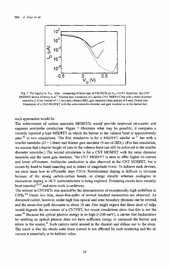
Fig. 7. The log(l,) vs. V,, plots comparing of three type of CNTFETs sat VDs = 0.4V. Solid line: the CNT MSDFET device of Javey et a1.” Dashed line: simulation of a similar CNT MSDFET but with a small diameter
nanotube (1 .O nm instead of 1.7 nm) and a thinner HfOz gate insulator (4nm instead of 8 nm). Dotted line: Simulation of a CNT MOSFET with the same nanotube diameter and gate insulator as in the dashed line.
such approaches would be. The achievement of carbon nanotube MOSFETs would provide improved on-current and suppress ambipolar conduction. Figure 7 illustrates what may be possible; it compares a recently reported p-type MSDFET in which the barrier to the valence band is approximately zero but with a smaller nanotube (D = 1 .Onm) and thinner gate insulator (4 nm of Hf02). (For this simulation, we assume that a barrier height of zero to the valence band can still be achieved in the smaller diameter nanotube.) The second simulation is for a CNT MOSFET with the same diameter nanotube and the same gate insulator. The CNT MOSFET is seen to offer higher on-current and lower off-current. Ambipolar conduction is also observed in the CNT MOSFET, but it occurs by band to band tunneling and is orders of magnitude lower. To achieve such devices, we must learn how to efficiently dope CNTs. Substitutional doping is difficult to envision because of the strong carbon-carbon bonds, so charge transfer schemes analogous to modulation doping in 111-V semiconductors is being explored. Promising results have recently been reported 25-2’ and more work is underway. The interest in CNTFETs was spurred by the demonstration of exceptionally high mobilities in CNTS.’,~ Under low bias, mean-free-paths of several hundred nanometers are observed. As discussed earlier, however, under high bias optical and zone boundary phonons can be emitted, and the mean-free-path decreases to about 10 nm. One might expect that these short of mfps would degrade the on-current of a CNTFET, but recent simulations show that this is not the case.’6 Because the optical phonon energy is so high (-200 meV), a carrier that backscatters by emitting an optical phonon does not have sufficient energy to surmount the barrier and return to the source.’6 Such carriers rattle around in the channel and diffuse out to the drain. The result is that the steady-state drain current is not affected by such scattering and the dc current is essentially at its ballistic value.
to two simulations. The first simulation is for a MSDFET similar to
24
Carbon Nanotube Field-Effect Transistors 907
5. Discussion
During the past few years, much has been learned about the physics of CNTFETs. Sophisticated device structures with high-lc gate dielectrics and self-aligned gate electrodes are now being reported.'* Contacts are still a challenge, especially low barrier contact to the conduction band. Techniques to achieve stable, high levels of doping will need to be developed so that high performance CNT MOSFETs can be produced. Our understanding of scattering is still incomplete; for example, the mean-free-paths computed from the expected electron-phonon coupling parameters 36764 are longer that the value deduced fiom experiments.33235v36 Hot phonon effects, which are a possible explanation for this discrepancy, need to be explored. Scattering in doped CNTs is also not understood. Javey et al.29 observed good transport properties after the tube is very heavily doped, but Appenzeller et al? observed a significant degradation of current due to doping. The future of CNTFETs will depend on two things, finding appropriate applications and developing high volume manufacturing technologies. Because of their excellent transport properties, RF applications of CNTFETs have been the subject of considerable recent While the dc performance of CNTFETs is now understood rather well, little is known about their RF performance. The band-structure limited velocity of -8x lo7 c d s is high and leads to expectations of THz performance. We have argued that phonon scattering has a small effect on the dc current of a CNTFET, but it does lead to dispersion in the transit time and should affect the ac performance. For RF applications, the MSDFET may be suitable, because leakage currents are not as important as in high density digital circuits. We still do not understand, however, how CNT MSDFETS and CNT MOSFETs compare for high-frequency applications. Other issues, such as the role that the so-called kinetic inductance 45v46 might play in such devices, also need to be explored.
6. Summary
Carbon nanotube field-effect transistors are interesting devices with potentially important applications in electronics. In this paper, we have summarized the current status of the field in terms of fabrication technology and device physics. The rate of progress in CNTFET technology and in the understanding of their device physics has been very rapid. Although uncertainties remain, the dc performance of field-effect transistors can now be explained. During the next few years, we expect to see increased work on other devices, for example, high-speed transistors, optoelectronics devices, and bio-sensors. We are sure to learn a good deal of interesting new device physics in the process and may even discover important technological applications.
Acknowledgements
The authors would like to thank Professor Mani Vaidyanathan of University of Alberta, Canada for many stimulating discussions. This work was supported by the National Science
25
908 J . Guo et al.
Foundation through the Network for Computational Nanotechnology and by the Microelectronics Advanced Research Corporation through the Focus Center on Materials, Structures, and Devices.
References
1. S . Iijima and T. Ichihashi, "Single-shell carbonmanotubes of 1-nm diameter," Nature, Vol.
2. D. S. Bethune, C. H. Kiang, M. S. Devries, G. Gorman, R. Savoy, J. Vazquez, and R. Beyers, "Cobalt-catalyzed growth of carbon nanotubes with single-atomic-layer walls," Nature, Vol. 363, pp. 605-607, 1993.
3. R. Saito, G. Dresselhaus, and M. Dresselhaus, Physical Properties of Carbon Nanotubes, Impreial College Press, 1998.
4. P. L. McEuen, M. S. Fuhrer, and Park Hongkun, "Single-walled carbon nanotube electronics," IEEE Trans. on Nanotechnology, Vol. 1, No. 1, pp. 78-85,2002.
5. T. Durkop, S. A. Getty, E. Cobas, and M .S. Fuhrer, "Extraordinary mobility in Semiconducting Carbon Nanotubes," Nano Letters, Vol. 04, No. 1, pp. 35-39,2004.
6. X. Zhou, J-Y. Park, S. Huang, J. Liu, and P. L. McEuen, "Band structure, phonon scattering, and the performance limit of single-walled carbon nanotube transistors," Physical Review Letters, Vol. 95, 146805, 2005.
7. J. A. Misewich, R. Martel, Ph. Avouris, J. C. Tsang, S. Heinze, and J. Tersoff, "Electrically induced optical emmision from a carbon nanotube FET," Science, Vol. 300, pp. 783-786, 2003.
8. M. Freitag, V. Perebeinos, J. Chen, A. Stein, J. C. Tsang, J. A. Misewich, R. Martel, P. Avouris, "Hot carrier electroluminescence from a single carbon nanotube", Nano Letters,
9. M. Freitag, J. Chen, J. Tersoff, J. C. Tsang, Q. Fu, J. Liu, and Ph. Avouris, "Mobile ambipolar domain in carbon-nanotube infrared emitters," Physical Review Letters, Vol. 93, No. 7,076803,2004.
10. S. J. Tans, A. R. M. Verschueren, and C. Dekker, "Room-temperature transistor based on a single carbon nanotube," Nature, Vol. 393, pp. 49-52, 1998.
11. R. Martel, T. Schmidt, H. R. Shea, T. Hertel, and P. Avouris, "Single- and multi-wall carbon nanotube field-effect transistors," Applied Physics Letters, Vol. 73, pp. 2447-2449, 1998.
12. A. Javey, J. Guo, D. B. Farmer, Q. Wang, E. Yenilmez, R. G. Gordon, M. Lundstrom, and H. Dai, "Self-aligned ballistic molecular transistors and parallel nanotube arrays," Nano Letters, Vol. 4, pp. 1319-1322,2004.
13.A. Thess, R. Lee, P. Nikolaev, H. Dai, P. Petit, J. Robert, C. Xu, Y. H. Lee, S. G. Kim, A. G. Rinzler, D. T. Colbert, G. E. Scuseria, D. Tomanek, J. E. Fischer, and R. E. Smalley, "Crystalline ropes of metallic carbon nanotubes," Science, Vol. 273, pp. 483-487, 1996.
14. J. Kong, H. T. Soh, A. M. Cassell, C. F. Quate, and H. Dai, "Synthesis of individual single-walled carbon nanotubes on patterned silicon wafers," Nature, Vol. 395, pp.
363, pp. 603-605, 1993.
Vol. 4,No. 6, pp. 1063-1066,2004.
878-881, 1998.
26
Carbon Nanotube Field-Effect Transistors 909
15. S.M. Sze, Physics of Semiconductor Device~,2"~ Edition, John Wiley & Sons, Inc., 1982. 16. S. Heinze, J. Tersoff, R. Martel, V. Derycke, J. Appenzeller, and P. Avouris, "Carbon
nanotubes as Schottky barrier transistors," Physical Review Letters, Vol. 89, No. 10, 106801,2002.
17. J. Appenzeller, J. Knoch, V. Derycke, R. Martel, S. Wind, and P. Avouris, "Field-modulated carrier transport in carbon nanotube transistors," Physical Review Letters, Vol. 89, No. 12, 126801,2002.
18. A. Javey, J. Guo, Q. Wang, M. Lundstrom, and H. J. Dai, "Ballistic carbon nanotube field-effect transistors," Nature, Vol. 424, pp. 654-657,2003.
19. S. J. Wind, M. Radosavljevic, J. Appenzeller, and P. Avouris, "Transistor structures for the study of scaling in carbon nanotubes," J. Vac. Sci. Technol. B, Vol. 21, No. 6, pp. 2856-2859, Nov/Dec 2003.
20. F. Nihey, H. Hongo, Y. Ochiai, M. Yudasaka, and S. Iijima, "Carbon-nanotube field-effect transistors with very high intrinsic transconductance," Japanese Journal of Applied Physics Part 2-Letters, Vol. 42, pp. L1288-L1291,2003.
2 1. J. Guo and M. S. Lundstrom, "A computational study of thin-body, double-gate, Schottky barrier MOSFETs," IEEE Transactions on Electron Devices, Vol. 49, pp. 1897-1902, 2002.
22. S. J. Wind, J. Appenzeller, and P. Avouris, "Lateral scaling in carbon-nanotube field-effect transistors," Physical Review Letters, Vol. 91, No. 5,058301, 2003.
23. A. Javey, J. Guo, D. B. Farmer, Q. Wang, D. Wang, R. G. Gordon, M. Lundstrom, and H. Dai, "Carbon nanotube field-effect transistors with integrated ohmic contacts and high-k gate dielectrics," Nano Letters, Vol. 4, pp. 447,2004.
24. Y. M. Lin, J. Appenzeller, and Ph. Avouris., "Novel structures enabling bulk switching in carbon nanotube FETs", 62"d Device Research Technical Conference Digest, pp. 133, University of Notre Dame, Notre Dame, Indiana, June 21-23, 2004.
25. J. Chen, C. Klinke, A. Afzali, K. Chan, and Ph. Avouris., "Self-aligned carbon nanotube transistors with novel chemical doping," IEDM Tech. Digest, pp. 695-698,2004.
26. M. Radosavljevic, J. Appenzeller, Ph. Avouris, and J. Knoch, "High performance of potassium n-doped carbon nanotube field-effect transistor," Applied Physics Letters, Vol.
27. A. Javey, R. Tu, D. B. Farmer, J. Guo, R. G. Gordon, and H. Dai, "High performance n-type carbon nanotube field-effect transistors with chemically doped contacts," Nan0 Letters, 2005, In Press.
28. S. J. Wind, J. Appenzeller, R. Martel, V. Derycke, and P. Avowis, "Vertical scaling of carbon nanotube field-effect transistors using top gate electrodes," Applied Physics Letters,
29. A. Javey, H. Kim, M. Brink, Q. Wang, A. Ural, J. Guo, P. McIntyre, P. McEuen, M. Lundstrom, and H. J. Dai, "High-k dielectrics for advanced carbon-nanotube transistors and logic gates," Nature Materials, Vol. 1, pp. 241-246,2002.
30. B. M. Kim, T. Brintlinger, E. Cobas, M. S. Fuhrer, H. M. Zheng, Z. Yu, R. Droopad, J. Ramdani, and K. Eisenbeiser, "High-performance carbon nanotube transistors on SrTi03/Si substrates," Applied Physics Letters, Vol. 84, pp. 1946-1948,2004.
84, NO. 18, pp. 3693-3695,2004.
Vol. 80, pp. 3817-3819,2002.
27
910 J . GUO et al.
31. S. Rosenblatt, Y. Yaish, J. Park, J. Gore, V. Sazonova, and P. L. McEuen, "High performance electrolyte gated carbon nanotube transistors," Nano Letters, Vol. 2, pp.
32. G. P. Siddons, D. Merchin, J. H. Back, J. K. Jeong, and M. Shim, "Highly efficient Gating and doping of carbon nanotubes with polymer electrolytes," Nano Letters, Vol. 4, pp.
33. Z. Yao, C. L. Kane, and C. Dekker, "High-field electrical transport in single-wall carbon nanotubes," Physical Review Letters, Vol. 84, pp. 2941-2944,2000.
34. T. Ando, H. Matsumura, and T. Nakanishi, "Theory of ballistic transport in Carbon Nanotubes," Physica B, Vol. 323, pp. 44,2002.
35. A. Javey, J. Guo, M. Paulsson, Q. Wang, D. Mann, M. Lundstrom, and H. J. Dai, "High-field quasiballistic transport in short carbon nanotubes," Physical Review Letters, Vol. 92, 106804,2004.
36. J. Y. Park, S. Rosenblatt, Y. Yaish, V. Sazonova, H. Ustunel, S. Braig, T. A. Arias, P. W. Brouwer, and P. L. McEuen, "Electron-phonon scattering in metallic single-walled carbon nanotubes," Nano Letters, Vol. 4, pp. 517-520,2004.
37. R. Seidel, A. P. Graham, E. Unger, G. S. Duesberg, M. Liebau, W. Steinhoegl, F. Kreupl, and W. Hoenlein, "High-current nanotube transistors," Nano Letters, Vol. 4, pp. 83 1-834, 2004.
38. W. B. Choi, B. H. Cheong, J. J. Kim, J. Chu, and E. Bae, "Selective growth of carbon nanotubes for nanoscale transistors," Advanced Functional Materials, Vol. 13, pp. 80-84, 2003.
39. R.H. Hendel, C.W. Tu, and R. Dingle, "Molecular beam epitaxy and the technology of selectively doped heterostructure transistors," Gallium Arsenide Technology, edited by R.K. Ferry, Howard W. Sams and Co., Indianapolis, 1985.
40. V. Derycke, R. Martel, J. Appenzeller, and P. Avouris, "Carbon nanotube inter- and intramolecular logic gates," Nano Letters, Vol. 1, pp. 453-456,2001.
41. A. Bachtold, P. Hadley, T. Nakanishi, and C. Dekker, "Logic circuits with carbon nanotube transistors," Science, Vol. 294, pp. 1317-1320, 2001.
42. D. J. Frank and J. Appenzeller, "High-frequency response in carbon nanotube field-effect transistors," IEEE Electron Device Letters, vol. 25, pp. 34-36, January 2004.
43. J. Appenzeller and D. J. Frank, "Frequency dependent characterization of transport properties in carbon nanotube transistors," Applied Physics Letters, Vol. 84, pp. 177 1-1 773, 2004.
44. S. D. Li, Z. Yu, S. F. Yen, W. C. Tang, and P. J. Burke, "Carbon nanotube transistor operation at 2.6 GHz," Nano Letters, Vol. 4, pp. 753-756,2004.
45. P.J. Burke, "Luttinger Liquid theory as a model of the gigahertz electrical properties of carbon nanotubes," IEEE Transactions on Nanotechnology, V01.2, No.1, pp. 129-144, Sept. 2002.
46. P.J. Burke, "An RF circuit model for carbon nanotubes," IEEE Transactions on Nanotechnology, V01.2, No.1, pp. 55-58, March. 2003.
47. P. J. Burke, "AC performance of nanoelectronics: Towards a ballistic THz nanotube transistor," Solid-state Electronics, 2004. In press.
869-872,2002.
927-93 1,2004.
28
Carbon Nanotube Field-Effect Transistors 911
48. D.L. John, L.C. Castro, J.P. Clifford and D.L. Pulfrey, “Electrostatics of coaxial Schottky-barrier nanotube field-effect transistors”, IEEE Trans. Nanotech., v01.2, 175-180, 2003.
49. G. Pennington and N. Goldsman, “Semiclassical transport and phonon scattering on electrons in semiconducting carbon nanotubes,” Phys. Rev. B, 68,045426,2003.
50. K. Alam and R. Lake, “Performance of 2nm gate length carbon nanotube field-effect transistors with sourceldrain underlaps,” Appl. Phys. Lett., vol. 87, p. 073 104, 2005.
51. A. Verma, M. Z. Kauser, and P. P. Ruden, “Ensemble Monte Carlo transport simulations for semiconducting carbon nanotubes,” J. Appl. Phys., vol. 97, p. 114319, 2005.
52. T. S. Xia, L. R. Register, and S. K. Banerjee, “Calculations and applications of the complex band structure for carbon nanotube field-effect transistors,” Phys. Rev. B, vol. 70, p. 045332,2004.
53. A. Svizhenko and M. P. Anantram, “Effect of scattering and contacts on current and electrostatics in carbon nanotubes,“ Phys. Rev. B., vol. 72, p. 085430,2005.
54. S. Datta, “Nanoscale device modeling: the Green’s method,” Superlattices and Microstructures, Vol. 28, pp. 253-278,2000.
55. M. Lundstrom, Fundamentals of Carrier Tranpsort, 2”d Edition, Cambridge University Press, Cambridge, UK, 2000.
56. Jing Guo, “Carbon Naotube Electronics: Modeling, Physics, and Applications,” Ph.D. Thesis, Purdue University, August, 2004.
57. S. Datta, “The Non equilibrium Green’s function (NEGF) formalism: an elementary introduction,” IEDM Tech. Digest, pp. 703-706, 2002.
58. R. Venugopal, Z. Ren, S. Datta, and M. Lundstrom, “Simulating quantum transport in nanoscale transistors: Real versus mode-space approaches,” Journal of Applied Physics,
59. J. Guo, S. Datta, M. Lundstrom, M. P. Anantram, “Multi-scale modeling of carbon nanotube transistors,”The international Journal on Multiscale Computational Engineering, Vol. 2,2004, In press.
60. J. Guo, A. Javey, H. Dai, S. Datta, and M. Lundstrom, “Predicted performance advantages of carbon nanotube transistors with doped nanotubes as sourceldrain,” Condense Matter, cond-mat/0309039: http:l/arxiv.org/abs/cond-mat/0309039,2003.
61. J. Guo, S. Datta, and M.S. Lundstrom, “A numerical study of scaling issues for Schottky barrier carbon nanotube transistors,” IEEE Trans. on Electron Devices, Vol. 51, pp.
62. A. Raychowdhury, J. Guo, K. Roy, and M. Lundstrom, “Choice of flat-band voltage, VDD and diameter of ambipolar Schottky-barrier carbon nanotube transistors in digital circuit design,” Proc. of the Fourth IEEE Nano Conference, Munich, Aug. 2004.
63. Y. M. Lin, J. Appenzeller, and Ph. Avouris., “Ambipolar-to-unipolar conversion of carbon nanotube transistors by gate structure engineering,” Nan0 Letters, Vol. 4, No. 5, pp.
64. G. D. Mahan, “Electron-optical phonon interactions in carbon nanotubes,” Physical
Vol. 92, NO. 7, pp. 3730-3739,2002,
172-177,2004.
947-950,2004.
Review B, Vol. 68, 125409,2003.
29
912 J . Guo et al.
65. J. Appenzeller, J. Knoch, M. Radosavljevic, and P. Avouris, “Multimode transport in Schottky-Barrier Carbon-Nanotube field effect transistors,” Physical Review Letters, Vol. 92, No. 22,226802, June 2004.
30
World Scientific www.worldsciefltific.com
International Journal of High Speed Electronics and Systems
@ World Scientific Publishing Company Vol. 16, NO. 4 (2006) 913-935
Carbon Nanotube Based Microwave Resonator Gas Sensors
M. P. McGRATH and A. PHAM
Microwave Microsystems Laboratory Dept. of Electrical and Computer Engineering
University of Calvornia at Davis, Davis, CA, USA
This paper reviews our work on the development of microwave carbon nanotube resonator sensors for gas
detection. The sensor consists of a radio frequency resonator coated with a layer of carbon nanotubes. Upon
exposure to gasses, the resonant frequency of the sensor shifts to indicate the presence of gasses. Our experimental
results demonstrate that the microwave carbon nanotube resonator sensor achieves a sensitivity of 4000 Hdppm upon
exposure to ammonia and the resonant frequency is recovered when ammonia is evacuated. The sensing mechanism
is dependent on electron transfer from the ammonia to the nanotubes. This sensor platform has great potential for
wireless sensing network applications.
Keywords: carbon nanotubes, wireless, sensor, and remote.
I. Introduction to Carbon Nanotube Gas Sensors
Chemical sensors are currently one of the most important research areas. The ability
to monitor our environment is becoming increasingly important. With the world market for
sensor microsystems estimated to be greater than $38 billion', the current demand is already
extraordinary with many applications yet to be realized. From improving the efficiencies of
industrial processes, to monitoring changes in our planet's ecosystem, and to ensure national
security the possibilities for reliable, sensitive, compact, and cost efficient sensors are
overwhelming. Despite many difficulties, the recent successes in the field carbon nanotube
chemical and biological sensors offer excellent promise in the near future.
Gas sensors have various implementations. The most common implementation to
date is the semiconductor sensor. Semiconductor sensors use the charge transfer f rodto an
impurity to/from the transducing material (the semiconductor). This causes a change in the
carrier concentration which manifests itself as a resistance change in the material. Metal
31
914 M . P . McGrath tY A . Pham
oxides are the most commonly used material with the main disadvantage being that they
require relatively high temperatures (-200 Co)2-'o. Another technique receiving a fair amount
of attention in recent years is the surface acoustic wave (SAW) sensors. Although
implemented on a platform suited for wireless applications, demonstrations of its utility as a
gas sensor have not been compelling due to low sensitivity''-23. Other techniques used for
gas sensing include optical fibers terminated or coated with a sensing material, infra-red
spectroscopy, and various mass spectroscopy techniques currently used in laboratories.
Although these methods are very precise, their size and cost prohibit them from wide
a~ceptance~~'~ ' . Another technique similar to semiconductor sensors is the use of
nano-structured sensors. Most of the nano-structured materials used are also semiconductors.
Currently, three of the most popular materials are nanobelts'' (suffering from the same
temperature restrictions as metal oxides), nanowires, and carbon nanotubes, the subject of this
paper.
Nanotechnology can offer solutions to scalability, integration, and sensitivity issues
that have plagued traditional technologies- a fact that was already recognized by Gopel in
19912'. In nanomaterial based sensors, sensitivity increases of six to eighteen orders of
magnitudes are theoretically and practically possible. The detection of single molecules by Cu
nanowire based sensors has already been reported3'. Sensing will also become much faster.
By introducing transducers with nanoscale dimensions, the lengths of electrical connections
are decreased, and sensing speeds can be increased substantially. Nanoscale phenomena such
as conductance quantization3' and single electron charging3* will be utilized for sensing
purposes. The required techniques (scanning tunneling microscopy (STM), atomic force
microscopy (AFM), near-field scanning optical microscopy and laser spectroscopy) for the
detection of these novel phenomena are already available.
Particular interest exists in using nanowires of semiconducting and metallic33' 34
materials as sensor elements. The advantage of these one-dimensional electrical conductors is
that they can be employed for both detection and signal transduction. Chemically modified
and non-modified nanowires for biochemical and gas sensor applications were fabricated by
Yang3' and Lieber36.
Similar applications have been realized with carbon nanotubes. As shown by Dai and
coworkers, 3' gases such as NO2 can change the electrical conductivity of carbon nanotubes by
three orders of magnitude even at a concentration of only 20 ppm. Collins38 obtained similar
results when exposing carbon nanotubes to oxygen. These reported sensitivities, as well as
very short response times, exceeded the performance of comparable solid-state sensors.
32
Carbon Nanotube Based Microwave Resonator Gas Sensors 915
Nano-structured materials have been used as the sensing material in three main
categories of sensors: the SAW sensor’” conductivity sensors, and spectral domain
sensors. SAW sensors, as mentioned above, suffer from the drawback of low sensitivity.
Conductivity sensors, on the other hand, have relatively high sensitivity and have been used
with a wide range of materials2-’’, 36-s2 . Conductivity sensors operate at DC and have two
common implementations. The first is simply using the sensing material as a resistor, and the
second involves using the material as the channel of a FET. Upon exposure to impurities, the
material will change its conductivity, which will be sensed as either a current or voltage
change. Conductivity sensors have been used with a wide range of materials. Metal oxides have had much success in gas sensing2-*’, but due to the temperature requirement, they are not
suited for wireless applications. Conductive polymers43’ s2-s3 and carbon nanotube~~’-~’’ 44-s’
have been demonstrated to operate at room temperature, and the use of mass selective polymer
coatingss3 offers potential of improving the sensitivity of nanotube based sensors. The
essential drawback with these sensors is their response time, which improves with
temperatures4.
Spectral domain sensor^^^-^^ are very similar to conductivity sensors, except that
changes in conductivity at a frequency or over a range of frequencies are used to determine the
concentration of impurities. These structures can simply be conductivity devices operated at
higher frequencies, where the concentration of the impurities would be deduced from the
changes in the ac transfer characteristics of the materiaf3. They can also be capacitors,
planar inductorss6, microwave re~onators~~-~’’ s8-63, or simply a terminated transmission line”.
The choice of where to put the sensing material on these structures depends on where it will
have the greatest effect on performance when its properties change as well as where it will be
the most exposed to the environment. Spectral domain sensors offer one significant
advantage over conductivity sensors in that they can operate at a frequency suited for wireless
transmission. Thus, impedance sensors are capable of creating wireless sensor nodes with
minimal complexity, as shown by Yoons5 and KongS6.
The remainder of this paper of consists of six sections. First we will present a brief
review of sensor terminology. Second, we will discuss the electrical properties of carbon
nanotubes, as well as a brief explanation of the sensing mechanism. Third, we will describe
the work we have done at U.C. Davis, providing a summary of our design process,
experimental setup, experimental results, and fbrther discussion regarding the sensing
mechanism. The remaining sections will review recent developments in wireless gas sensing
nodes, functionalizing carbon nanotubes for specific applications, and, finally, describe our
33
916 M. P. McGrath €4 A . Pham
future research in the development of the microwave carbon nanotube resonator sensors.
11. Review of Gas Sensor Terminology
Gas sensors must meet a variety of criteria in order to be practical. The sensor must
respond within a relatively short time period to give an accurate assessment of the current
impurity concentration. Response time is usually used to specify the time interval required
for the sensor to stabilize at its final value. Other terms are sometimes used to characterize
the response time such as rise time. This term is used to characterize the time required for the
sensor response to reach a certain percentage of its final value.
Sensors should also be reusable for wide acceptance. The characterization of how
long the sensor takes to return to its initial state is its recovery time. Recovery time generally
refers to the amount of time required for the sensor to stabilize at its initial state. Fall time (or
rise time depending of the sensors response) may also be used and refers to the time interval
required for the sensor to return to some percentage, usually ninety, of its initial state.
Recovery is one of the main obstacles of carbon nanotube based sensors, which can take
several hours.
Sensitivity is used to characterize the change in the sensor’s response for a given
concentration of gas. Obviously, the amount of changes for a given concentration of gas is of
primary importance. In this paper sensitivity will refer to the sensor response, characterized
by frequency shift, divided by the concentration in ppm. The linear range of the sensor
response corresponds to a range of concentrations for which the sensitivity is constant.
Linearity in the response is desirable. However, as long as the response is monotonic, and
repeatable, this is not a major concern. Another parameter related to sensitivity is selectivity.
Not only must the sensor be highly sensitive, but it must be sensitive only to the impurities of
interest to avoid false alarms.
111. Properties of Carbon Nanotubes and Mechanisms for Gas Sensing
Carbon nanotubes have very high aspect ratios and are essentially all surface area.
The two main aspects of nanotubes that determine their electrical properties are diameter and
chirality. If the nanotube is envisioned as rolled graphite sheet, the tube’s chirality is
determined by how the sheet attaches to itself. The chiral vector is defined as Ck=nxal+mxa2
(see Figure 1.) and is between two equivalent sites representing where the graphite sheet
attaches to itself to form the nanotube. The vector is directed along the circumference of the
34
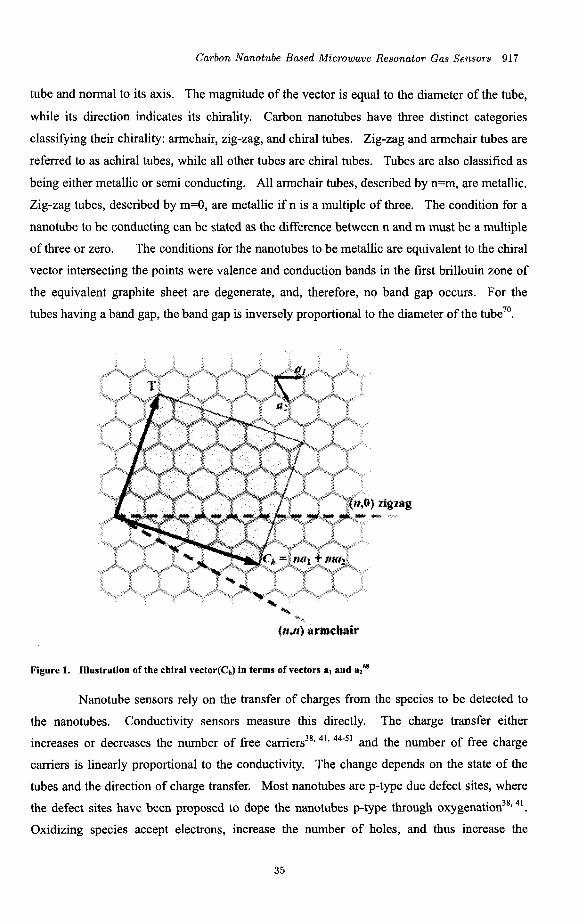
Carbon Nanotube Based Microwave Resonator Gas Sensors 917
tube and normal to its axis. The magnitude of the vector is equal to the diameter of the tube,
while its direction indicates its chirality. Carbon nanotubes have three distinct categories
classifying their chirality: armchair, zig-zag, and chiral tubes. Zig-zag and armchair tubes are
referred to as achiral tubes, while all other tubes are chiral tubes. Tubes are also classified as
being either metallic or semi conducting. All armchair tubes, described by n=m, are metallic.
Zig-zag tubes, described by m=O, are metallic if n is a multiple of three. The condition for a
nanotube to be conducting can be stated as the difference between n and m must be a multiple
of three or zero. The conditions for the nanotubes to be metallic are equivalent to the chiral
vector intersecting the points were valence and conduction bands in the first brillouin zone of
the equivalent graphite sheet are degenerate, and, therefore, no band gap occurs. For the
tubes having a band gap, the band gap is inversely proportional to the diameter of the tube”.
Figure 1. Illustration of the chiral vector(C,,) in terms of vectors a, and 816’
Nanotube sensors rely on the transfer of charges from the species to be detected to
the nanotubes. The charge transfer either
increases or decreases the number of free carriers383 41* 44-51 and the number of free charge
carriers is linearly proportional to the conductivity. The change depends on the state of the
tubes and the direction of charge transfer. Most nanotubes are p-type due defect sites, where
the defect sites have been proposed to dope the nanotubes p-type through ox~genat ion~~’ 41.
Oxidizing species accept electrons, increase the number of holes, and thus increase the
Conductivity sensors measure this directly.
35
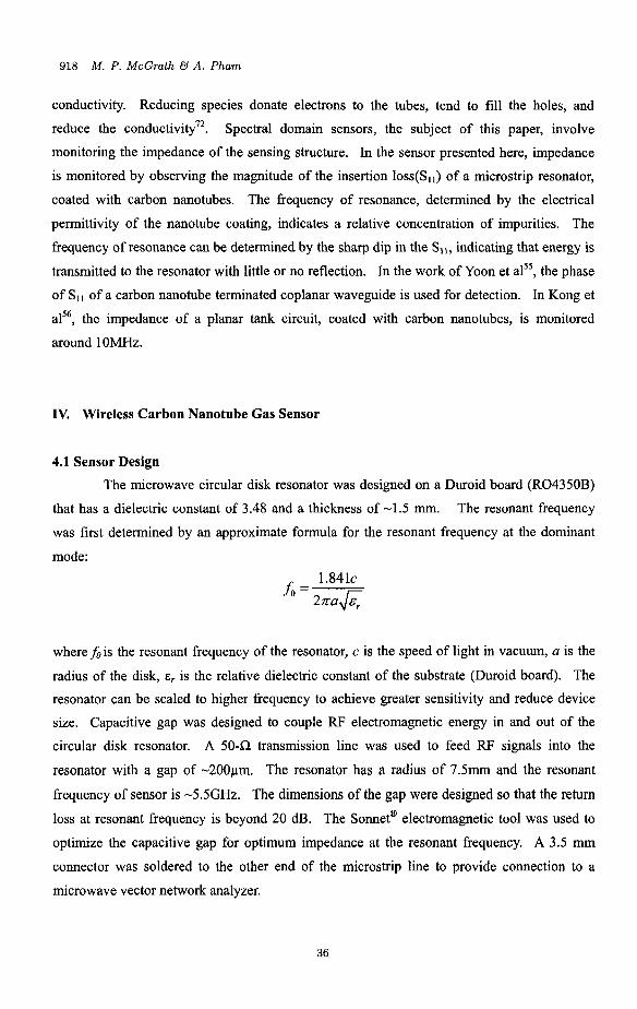
918 M . P. McGrath & A . Pham
conductivity. Reducing species donate electrons to the tubes, tend to fill the holes, and
reduce the conductivity'*. Spectral domain sensors, the subject of this paper, involve
monitoring the impedance of the sensing structure. In the sensor presented here, impedance
is monitored by observing the magnitude of the insertion loss(SI1) of a microstrip resonator,
coated with carbon nanotubes. The frequency of resonance, determined by the electrical
permittivity of the nanotube coating, indicates a relative concentration of impurities. The
frequency of resonance can be determined by the sharp dip in the S11, indicating that energy is
transmitted to the resonator with little or no reflection. In the work of Yoon et alS5, the phase
of Sll of a carbon nanotube terminated coplanar waveguide is used for detection. In Kong et
alS6, the impedance of a planar tank circuit, coated with carbon nanotubes, is monitored
around 1OMHz.
IV. Wireless Carbon Nanotube Gas Sensor
4.1 Sensor Design The microwave circular disk resonator was designed on a Duroid board (R04350B)
that has a dielectric constant of 3.48 and a thickness of -1.5 mm. The resonant frequency
was first determined by an approximate formula for the resonant frequency at the dominant
mode:
where& is the resonant frequency of the resonator, c is the speed of light in vacuum, a is the
radius of the disk, E, is the relative dielectric constant of the substrate (Duroid board). The
resonator can be scaled to higher frequency to achieve greater sensitivity and reduce device
size. Capacitive gap was designed to couple RF electromagnetic energy in and out of the
circular disk resonator. A 5042 transmission line was used to feed RF signals into the
resonator with a gap of -200pm. The resonator has a radius of 7.5mm and the resonant
frequency of sensor is -5.5GHz. The dimensions of the gap were designed so that the return
loss at resonant frequency is beyond 20 dB. The Sonnet@' electromagnetic tool was used to
optimize the capacitive gap for optimum impedance at the resonant frequency. A 3.5 mm
connector was soldered to the other end of the microstrip line to provide connection to a
microwave vector network analyzer.
36
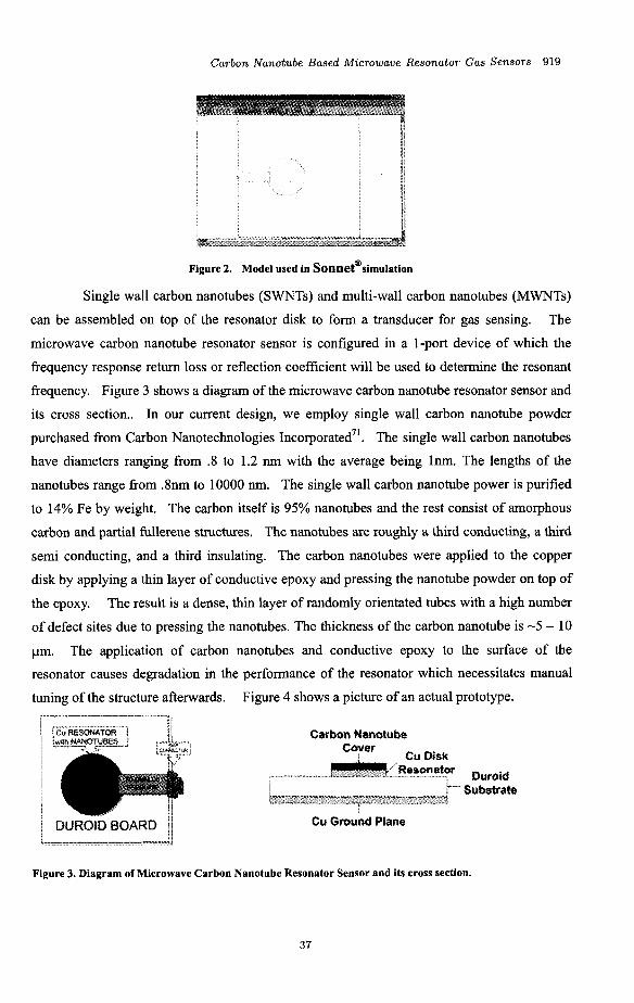
Carbon Nanotube Based Microwave Resonator Gas Sensors 919
I
Figure 2. Model used in SOnnet@simulation
Single wall carbon nanotubes (SWNTs) and multi-wall carbon nanotubes (MWNTs)
can be assembled on top of the resonator disk to form a transducer for gas sensing. The
microwave carbon nanotube resonator sensor is configured in a 1-port device of which the
frequency response return loss or reflection coefficient will be used to determine the resonant
frequency. Figure 3 shows a diagram of the microwave carbon nanotube resonator sensor and
its cross section.. In our current design, we employ single wall carbon nanotube powder
purchased from Carbon Nanotechnologies Incorporated7'. The single wall carbon nanotubes
have diameters ranging from .8 to 1.2 nm with the average being lnm. The lengths of the
nanotubes range from .8nm to 10000 nm. The single wall carbon nanotube power is purified
to 14% Fe by weight. The carbon itself is 95% nanotubes and the rest consist of amorphous
carbon and partial fullerene structures. The nanotubes are roughly a third conducting, a third
semi conducting, and a third insulating. The carbon nanotubes were applied to the copper
disk by applying a thin layer of conductive epoxy and pressing the nanotube powder on top of
the epoxy. The result is a dense, thin layer of randomly orientated tubes with a high number
of defect sites due to pressing the nanotubes. The thickness of the carbon nanotube is -5 - 10
pm. The application of carbon nanotubes and conductive epoxy to the surface of the resonator causes degradation in the performance of the resonator which necessitates manual
tuning of the structure afterwards. Figure 4 shows a picture of an actual prototype. r - - - - - - - - - -
Carbon Nanotube
Cu Ground Plane
Figure 3. Diagram of Microwave Carbon Nanotube Resonator Sensor and its cross section.
37
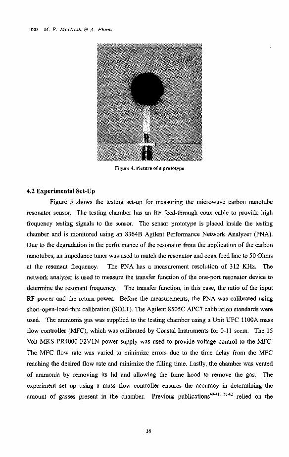
920 M. P . McGrath B A . Pham
Figure 4. Picture of a prototype
4.2 Experimental Set-Up
Figure 5 shows the testing set-up for measuring the microwave carbon nanotube
resonator sensor. The testing chamber has an RF feed-through coax cable to provide high
frequency testing signals to the sensor. The sensor prototype is placed inside the testing
chamber and is monitored using an 8364B Agilent Performance Network Analyzer (PNA).
Due to the degradation in the performance of the resonator from the application of the carbon
nanotubes, an impedance tuner was used to match the resonator and coax feed line to 50 Ohms
at the resonant frequency. The
network analyzer is used to measure the transfer function of the one-port resonator device to
determine the resonant frequency. The transfer function, in this case, the ratio of the input
RF power and the return power. Before the measurements, the PNA was calibrated using
short-open-load-thru calibration (SOLT). The Agilent 8505C APC7 calibration standards were
used. The ammonia gas was supplied to the testing chamber using a Unit UFC llOOA mass
flow controller (MFC), which was calibrated by Coastal Instruments for 0-11 sccm. The 15
Volt MKS PR4000-F2VlN power supply was used to provide voltage control to the MFC.
The MFC flow rate was varied to minimize errors due to the time delay from the MFC
reaching the desired flow rate and minimize the filling time. Lastly, the chamber was vented
of ammonia by removing its lid and allowing the fume hood to remove the gas. The
experiment set up using a mass flow controller ensures the accuracy in determining the
amount of gasses present in the chamber. Previous publications4041s ''4' relied on the
The PNA has a measurement resolution of 312 KHz.
38
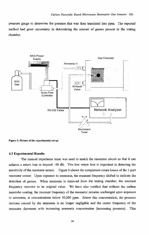
Carbon Nanotube Based Microwave Resonator Gas Sensors 921
RS-232 Cable
pressure gauge to determine the pressure that was then translated into ppm. The reported
method had great uncertainty in determining the amount of gasses present in the testing
chamber.
~
Network Analyzer
j-:l Gas
MKS Power Supply
i
Gas Chamber
Ammonia In n-m
Ihd
Figure 5. Picture of the experimental set-up
4.3 Experimental Results
The manual impedance tuner was used to match the resonator circuit so that it can
achieve a return loss to beyond -40 dB. This low return loss is important in detecting the
sensitivity of the resonator sensor. Figure 6 shows the comparison return losses of the 1-port
resonator sensor. Upon exposure to ammonia, the resonant frequency shifted to indicate the
detection of gasses. When ammonia is removed from the testing chamber, the resonant
frequency recovers to its original value. We have also verified that without the carbon
nanotube coating, the resonant frequency of the resonator remains unchanged upon exposure
to ammonia, at concentrations below 30,000 ppm. Above this concentration, the pressure
increase caused by the ammonia is no longer negligible and the center frequency of the
resonator decreases with increasing ammonia concentration (increasing pressure). This
39
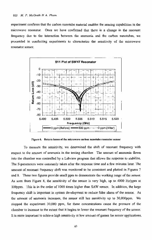
922 M. P. McGrath €3 A . Pham
experiment confirms that the carbon nanotube material enables the sensing capabilities in the
microwave resonator. Once we have confirmed that there is a change in the resonant
frequency due to the interaction between the ammonia and the carbon nanotubes, we
proceeded in conducting experiments to characterize the sensitivity of the microwave
resonator sensor.
S11 Plot of SWNT Resonator
0
-10
-20
-30 m
fn fn 5 -40 5 -50
d -60 .I-
-70
-80 5.490 5.495 5.500 5.505 5.510 5.515 5.520
Frequency ( G k )
-0 ppm (Before) -500 ppm -0 ppm(After)
Figure 6. Return losses of the microwave carbon nanotube resonator sensor
To measure the sensitivity, we determined the shift of resonant frequency with
respect to the amount of ammonia in the testing chamber. The amount of ammonia flown
into the chamber was controlled by a Labview program that allows the response to stabilize.
The S-parameters were constantly taken after the response time and a few minutes later. The
amount of resonant frequency shift was monitored to be consistent and plotted in Figures 7
and 8. These two figures provide small ppm to demonstrate the working range of the sensor.
As seen from Figure 8, the sensitivity of the sensor is very high, up to 4000 Hdppm at
100ppm. This is in the order of 1000 times higher than SAW sensor. In addition, the large
frequency shift is important in system development to reduce false alarm of the sensor. As
the amount of ammonia increases, the sensor still has sensitivity up to 30,000ppm. We
stopped the experiment 30,000 ppm, for these concentrations cause the pressure of the
chamber to increase to the extent that it begins to lower the resonant frequency of the sensor.
It is more important to achieve high sensitivity at low amount of gasses for sensor applications.
40
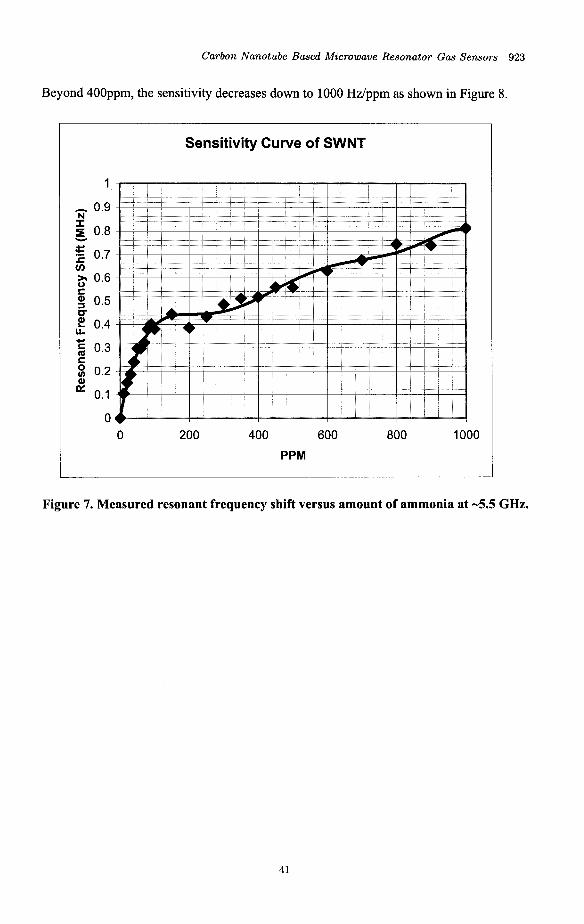
Carbon Nanotube Based Microwave Resonator Gas Sensors 923
Beyond 400ppm, the sensitivity decreases down to 1000 Hdppm as shown in Figure 8.
Sensitivity Curve of SWNT
1
h 0.9
0.8
0.7 v) 2 0.6 S 5 0.5 u 2 0.4 u. 5 0.3
N I v
c
E g 0.2
0.1
0 0 200 400 600 800 1000
PPM
Figure 7. Measured resonant frequency shift versus amount of ammonia at -5.5 GHz.
41
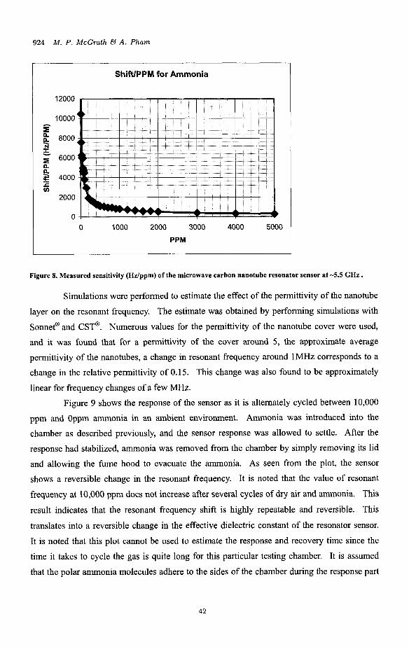
924 M . P. McGrath €4 A . Pham
ShiftlPPM for Ammonia
12000
10000
8000
6000
3 4000 x v)
2000
0
a % z I,
0 1000 2000 3000 4000 5000
PPM
Figure 8. Measured sensitivity (Hz/ppm) of the microwave carbon nanotuhe resonator sensor at -5.5 GHz .
Simulations were performed to estimate the effect of the permittivity of the nanotube
layer on the resonant frequency. The estimate was obtained by performing simulations with
Sonnet@ and CST@. Numerous values for the permittivity of the nanotube cover were used,
and it was found that for a permittivity of the cover around 5, the approximate average
permittivity of the nanotubes, a change in resonant frequency around lMHz corresponds to a
change in the relative permittivity of 0.15. This change was also found to be approximately
linear for frequency changes of a few MHz.
Figure 9 shows the response of the sensor as it is alternately cycled between 10,000
ppm and Oppm ammonia in an ambient environment. Ammonia was introduced into the
chamber as described previously, and the sensor response was allowed to settle. After the
response had stabilized, ammonia was removed from the chamber by simply removing its lid
and allowing the fume hood to evacuate the ammonia. As seen from the plot, the sensor
shows a reversible change in the resonant frequency. It is noted that the value of resonant
frequency at 10,000 ppm does not increase after several cycles of dry air and ammonia. This result indicates that the resonant frequency shift is highly repeatable and reversible. This
translates into a reversible change in the effective dielectric constant of the resonator sensor.
It is noted that this plot cannot be used to estimate the response and recovery time since the
time it takes to cycle the gas is quite long for this particular testing chamber. It is assumed
that the polar ammonia molecules adhere to the sides of the chamber during the response part
42
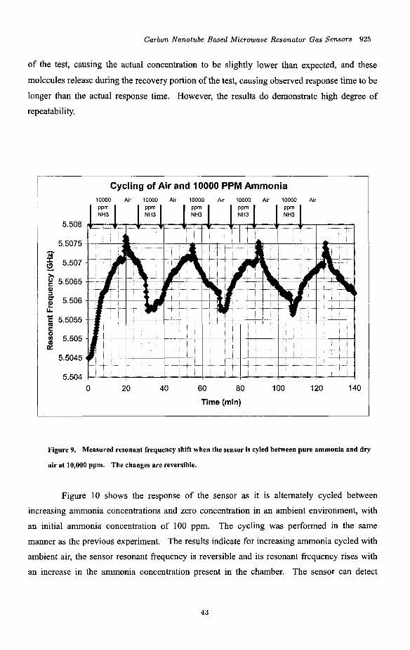
Carbon Nanotube Based Microwave Resonator Gas Sensors 925
of the test, causing the actual concentration to be slightly lower than expected, and these
molecules release during the recovery portion of the test, causing observed response time to be
longer than the actual response time. However, the results do demonstrate high degree of
repeatability.
Cycling of Air and 10000 PPM Ammonia
5.508
5.5075 ' 5.507
5.5065
5.506
5.5055
5.505
5.5045
5.504
- 9 21
a z
I&
tu C 0
d
0 20 40 60 80 100 120 140
Time (min)
Figure 9. Measured resonant frequency shift when the sensor is cyled between pure ammonia and dry
air at 10,000 ppm. The changes are reversible.
Figure 10 shows the response of the sensor as it is alternately cycled between
increasing ammonia concentrations and zero concentration in an ambient environment, with
an initial ammonia concentration of 100 ppm. The cycling was performed in the same
manner as the previous experiment. The results indicate for increasing ammonia cycled with
ambient air, the sensor resonant frequency is reversible and its resonant frequency rises with
an increase in the ammonia concentration present in the chamber. The sensor can detect
43
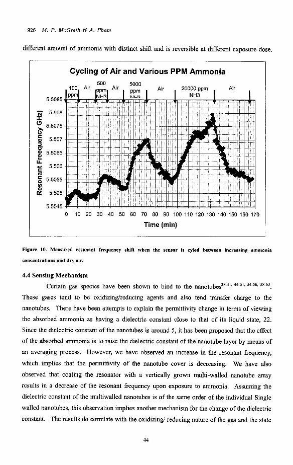
926 M. P. McGrath tY A . Pham
different amount of ammonia with distinct shift and is reversible at different exposure dose.
Cycling of Air and Various PPM Ammonia
5.5085
5.508
5.5075
s 5.507 S v Q) 5.5065
L u 5.506 c m
5.5055
d 5.505
5.5045
h P 6
g,
0 10 20 30 40 50 60 70 80 90 100 110 120 130 140 150 160 170
Time (min)
Figure 10. Measured resonant frequency shift when the sensor is cyled between increasing ammonia
concentrations and dry air.
4.4 Sensing Mechanism
Certain gas species have been shown to bind to the n a n o t u b e ~ ~ ~ - ~ ” 44-5’9 54-56, 58-63.
These gases tend to be oxidizing/reducing agents and also tend transfer charge to the
nanotubes. There have been attempts to explain the permittivity change in terms of viewing
the absorbed ammonia as having a dielectric constant close to that of its liquid state, 22.
Since the dielectric constant of the nanotubes is around 5, it has been proposed that the effect
of the absorbed ammonia is to raise the dielectric constant of the nanotube layer by means of
an averaging process. However, we have observed an increase in the resonant frequency,
which implies that the permittivity of the nanotube cover is decreasing. We have also
observed that coating the resonator with a vertically grown multi-walled nanotube array
results in a decrease of the resonant frequency upon exposure to ammonia. Assuming the
dielectric constant of the multiwalled nanotubes is of the same order of the individual Single
walled nanotubes, this observation implies another mechanism for the change of the dielectric
constant. The results do correlate with the oxidizing/ reducing nature of the gas and the state
44
Carbon Nanotube Based Microwave Resonator Gas Sensors 927
of the nanotube coating. Ammonia, a reducing agent, donates electrons to the nanotube”.
Since the single walled nanotube coating is p-type due to the effect of the donated
electrons tend to cancel out the holes and thus reduce the conductivity. The vertically grown
array of Multi-walled nanotubes yields relatively pristine, defect free, tubes. Since
oxygenation has been shown to occur at the defect sites4’, the lack of defect sites indicates the
tubes should be virtually intrinsic, so donated electrons increase the conductivity and
permittivity. This change in conductivity manifest it self in a change in permittivity. The
imaginary part and real parts of the permittivity increase monotonically with conductivity. In
reference 73, the permittivity of metallic nanotubes was found to increase proportionally to
the square of the Fermi level, with a positive additive term reflecting the increase of carrier
concentration with temperature. The results here suggest that for our nanotube coating,
consisting of tubes with a wide range of properties, that the carrier density is the dominant
factor. Although it may seem counterintuitive that conductivity affects the real part of the
permittivity, the Kramers-Kronig relations suggest that in order for the permittivity to be a real,
causal function, the imaginary and real parts are related. If the effect of the added charge was
to simply increase the conductivity over the entire frequency range or to only increase the low
frequency conductivity, the transformations suggest the results presented here. However,
detailed data on the frequency dependence of the conductivity is unavailable, and the exact
relationship between the change in conductivity and the real part of the permittivity has yet to
be determined. That relationship may also serve to explain the small percentage change of
resonant frequency in this resonant sensor compared to the order of magnitude change of DC
conductivity in conductivity sensors. In summary, the effect of an increase in conductivity
results in an increase of loss, a decrease in Q, an increase in the effective dielectric constant,
and an decrease in the resonant frequency. A decrease in conductivity should cause the
opposite effect.
45
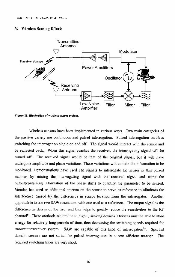
928 M. P. McGrath Ed A . Pham
V. Wireless Sensing Efforts
Transm itti na Antenna
Passive Sensor
Receivina Antenna
Power AmDlifiers
LOW Noise Filter Mixer Filter Amdifier
Figure 11. Illustration of wireless sensor system.
Wireless sensors have been implemented in various ways. Two main categories of
the passive variety are continuous and pulsed interrogation. Pulsed interrogation involves
switching the interrogation single on and off. The signal would interact with the sensor and
be reflected back. When this signal reaches the receiver, the interrogating signal will be
turned off. The received signal would be that of the original signal, but it will have
undergone amplitude and phase variations. These variations will contain the information to be
monitored. Demonstrations have used FM signals to interrogate the sensor in this pulsed
manner, by mixing the interrogating signal with the received signal and using the
output(containing information of the phase shift) to quantify the parameter to be sensed.
Varadan has used an additional antenna on the sensor to serve as reference to eliminate the
interference caused by the differences in sensor location from the interrogator. Another
approach is to use two SAW resonators, with one used as a reference. The output signal is the
difference in delays of the two, and this helps to greatly reduce the sensitivities to the lU? channelp4. These methods are limited to high Q sensing devices. Devices must be able to store
energy for relatively long periods of time, thus decreasing the switching speeds required for
transmitterlreceiver system. Spectral
domain sensors are not suited for pulsed interrogation in a cost efficient manner. The
required switching times are very short.
SAW are capable of this kind of interr~gation’~.
46
Carbon Nanotube Based Microwave Resonator Gas Sensors 929
The other type of interrogation is characterized by a continuous interrogating signal.
Kong et a1 have demonstrated this with carbon nanotube coated LC-tank sensor by monitoring
the impedance of a loop antenna in the vicinity of the sensor with an impedance analyzer56.
Similar results have been obtained by Yoon, with FM modulation of the interrogating signal55.
Although this has been shown to work, it is very sensitive on the location of the sensor, as
well as environmental factors affecting the RF channel. The ideal situation would be to
modulate the information onto the carrier signal at the sensor itself.
VI. Carbon Nanotube Functionalization Efforts
Although nanotubes have been shown here to be significantly sensitive to Ammonia,
as well as NO2 and other toxic substances elsewhere, many substances that are of interest do
not react significantly with the intrinsic nanotubes. Also, it is desirable to increase
sensitivity, selectivity, increase response time, and decrease recovery time. Nanotubes have
been functionalized by various means to address these issues for different application^^^-^^. Nanotubes doped with nitrogen ( CN, tubes) have been used in conductivity sensors and have
shown responses to relatively high concentrations (>1%) of ammonia, acetone, ethanol,
gasoline, pyridine, and ch1orofo1-m~~. Nanotubes have been doped with
poly-m-aminobenzene sulfonic acid for use in a conductivity sensor, resulting in a reported
two-fold increase in sensitivity to ammonia77. Tin Oxide coatings of 1-6nm have also been
reported for n a n ~ t u b e s ~ ~ ’ 78. Sensors have been constructed with these structures with
responses for ppm concentrations of NO, N02, ethanal, and CZH2. Nanotubes have been used
in conjuction with a Pd thin film for hydrogen detection with some success79. Doping
nanotubes with Pd has been demonstrated to be very effective, with sensitivities to .5% Hz in a
nitrogen environment8’. However, these tin oxide and palladium functionalized sensors do
require temperatures in excess of 200 C’. Amidoferrocenyl-fimctionalized nanotubes have
been demonstrated to recognize the presence of mM concentrations of HzP04- at room
tem~era ture~~. Room temperature responses have been observed for 6ppm of methanol with
Pd loaded carbon nanotubes6’. Peng and Cho have shown the possible detection of CO with
carbon nanotubes doped with boron and nitrogen, and they have also suggested that sensitivity
can be controlled through doping6’. Further research is needed to see if other molecules
could be used to aid selective reactivity at room temperature and ambient conditions. It has
been shown that the charge transfer to nanotubes depends on their chirality, and that metallic
tubes have the fastest rate of charge transfer. It was also shown that the smallest band gap
47
930 M . P. McGrath €9 A . Pham
tubes have a tenfold increase in their charge transfer rate, implying the ability to tune
responseh-ecovery timess4. Although constructing a layer of tubes of a single chirality is a
daunting task, chiral selective charge transfer offers hope in improving our ability to select
tubes of specific properties in the future.
VII. Future Research
Our research efforts are focused on developing a robust wireless sensor node with
tunable selectivity. Wireless sensing has been demonstrated, but there is still progress to be
made in reliability and cost reduction. Our current research regarding the wireless aspect of
this project involves reducing the sensitivity of the wireless node to its environment, while
increasing its sensitivity with respect to the species to be detected. The main challenge for
the wireless aspect of the node is the sensitivity of the RF channel to the surrounding
environment and the dependence of the measurand to the RF channel. Also, we are
investigating ways in which to make the carbon nanotubes a suitable transducer for a wider
range of species through fictionalization and increasing its selectivity either through
fictionalization or mass selective polymer coatings.
Acknowledgements
We acknowledge the support of National Science Foundation under contract ECS-0401375 and Professors Andre Knoesen and Diego Yankelvich at UC Davis.
References
1.
2.
3.
4.
5.
E. Mounier, “Microsystems for transportation: an overview of the different applications,” Control in Transportation Systems 2000. Proceedin s volume from the 9th IFAC Symposium, Elsevier Sci. Part vol. 1,200 1, pp.5 1-4 vol. f Kidlington, UK R Martins, E Fortunato, P Nunes, I Ferreira, A Marques, M Bender, N Katsarakis, V Cimalla, G Kiriakidis, “Zinc oxide as an ozone sensor,” Journal of Applied Physics, vo1.96, no.3, 1 Aug. 2004, pp.1398-408. Publisher: AIP, USA. G. Korotcenkov. “Gas resDonse control through structural and chemical modification of metal oxide f ihs : state o’f the art and approaches,” Sensors and Actuators B-Chemical 107 (1): 209-232 MAY 2005 G. Eranna, B. C. Joshi, D. P. Runthala, R. P. Gupta, “Oxide materials for develo ment of integrated gas sensors - A com rehensive review” Critical Reviews in Solid &ate and Material Sciences, 29 (3-4): 11 1-788 2004 A. V. Salker, N. J. Choi, J. H. Kwak, B. S. Joo, D. D. Lee, “Thick films of In, Bi and Pd metal oxides im regnated in L a c 0 0 3 erovskite as carbon monoxide sensor”, Sensors and Acuators B-Ehemical, 106 (1): 46 1867 APR 29 2005
48
Carbon Nanotube Based Microwave Resonator Gas Sensors 931
G. Korotcenkov, V. Macsanov, V. Brinzari, V. Tolstoy, J. Schwank. A. Comet, J. Morante, “Influence of ,Cu-,, Fe-, Co-, and Mn-oxide nanoclusters on sensing behavior of Sn02 films,” Thin Solid Films, 467 (1-2): 209-2 14 NOV 22 2004 T. Skala, K. Veltruska, M. Moroseac, I. Matolinova, G. Korotchenkov, V. Matolin, “Study of Pd-In interaction during Pd deposition on pyrolytically prepared In203,” Applied Surface Science, 205 (1-4): 196-205 Jan 3 1 2003 I. Kocemba, S. Szafian, J. R kowski, T. Pa ’czak, “Relationshi between the catalytic and detection properties o P S n 0 2 and P 8 n O 2 systems” Afsorption Science and Technology, 20 (9): 897-905 2002 C. Yu, Q. Hao, S. Saha, L. Shi, X. Y. Kon , Z. L. Wang, “Inte ration of metal oxide
Art. No. 063 101 FEB ? 2005 nanobelts with micros stems for nerve agent 9 etection,” Applied P i ysics Letters, 86 (6):
10. Z. L. Wang, “Functional oxide nanobelts: Materials, pro erties and potential a plications in nanosystems and biotechnology,” Annual Review of ghysical Chemistry, 5P: 159-196 2004
11. A. C. Fechete, S. J. Ippolito, K. Kalantar-zadeh, W. Wlodarski, A. S. Holland, K. Galatsis, G. Kiriakidis, N. Katsarakis, M. Katharakis, “The stud of InO,/ZnO/XZ LiNb03 layered SAW devices for ozone sensing,” Proceedings of the h E E Sensors 2004 . IEEE. Part vo1.3,2004, pp.1510-13 ~01.3.
12. L. M. Reindl, A. Pohl, G. Scholl, and R. Weigel, “SAW-based radio sensor systems,” IEEEE Sensor Journal, vol. 1, no. 1, pp. 69-78, June 2001.
13. A. Pohl, G. Osterma er, and F. Seifert, “Wireless sensing using oscillator circuits locked to remote high-Q S A d resonators,” IEEE Transactions on Ultrasonics, Ferroelectrics, and Fre uenc Control, vol. 45, no. 5, 1161-1168, Se t. 1998.
14. L. Ie indI G. Scholl, T. Ostertag, H. Scherr, 6. Wolff, and F. Schmidt, “Theory and a lication of passive SAW radio transponders as sensors,” IEEE Transactions on rf;!rasonics, Ferroelectrics, and Frequency Control, vol. 45, no. 5, pp. 1281-1291, Sept. 1998.
15. W. Jakubik, M. Urbanczyk, “H drogen, detection in surface acoustic based on interaction s eed,” Jroceedings of the IEEE Sensors No.04CH37603). IEEE. Hart vo1.3,2004, pp.1514-17 vo1.3. Piscataway,
Eng. Proceedin s of Spie - the International Society B or Optical Engineering, ~01.5274,
16. S. Ahmadi, F. Hassani, C. Korman, M. Rahaman, M., Zaghloul, “Characterization of multi- and single-la er structure SAW sensor,” Proceedin s of the IEEE Sensors 2004. IEEE. Part vo1.3,2084, pp.1129-32 vo1.3. Piscataway, NJ, &A.
17. S. J. Ippolito, S. Kandasamy, K. Kalantar-zadeh, W. Wlodarski, A. Holland, “Comparison between conductometric and layered SAW hydrogen as sensor,” SPIE-Int. SOC. 0 t.
no.l,31 Dec. 2%03, 18. J. Reibel, U. Stahl, T. Wessa, M. Rapp, “Gas analysis with SAW sensor systems,”
Elsevier. Sensors & Actuators B-Chemical, vol.B65, no. 1-3, 30 June 2000, pp.173-5. Switzerland.
19. M. Penza, E. Milella, V. I. Amsimkin, L. Vasanelli, “Surface acoustic wave (SAW) NH3 as sensor based on Langmuir-Blodgett polypyrrole film,” Proceedings of the 2nd Italian
Eonference on Sensors and. Microsystems. Artificial and Natural Perception. World Scientific. 1997, pp. 148-52. Singapore.
20. M. Penza, L. Vasanelli, “ SAW NO, as sensor usin W03 thin-film sensitive coating,” Sensors & Actuators B-Chemical, v o d 4 1 , no.1-3, 30fune 1997, pp.31-6
21. M. Hamsch, R. Hoffmann, W. Buff, M. Binhack, S. Klett, “An interrogation unit for assive wireless SAW sensors based on Fourier transform,” IEEE Transactions on
btrasonics Ferroelectrics & Frequency Control, vo1.5 1, no. 11, Nov. 2004, pp.1449-56. Publisher: IEEE, USA.
22. M. Peqa, G. Cassano, P. Aversa, F. Antolini, A. Cusano, M. Consales, M. Giordano, L. Nicolais, “Acoustic and optical sensors inco orating carbon nanotubes for detection of organic solvents,,” Proceedin s of the IEE8 Sensors 2004. IEEE. Part vol.1, 2004, pp.403-6 vol. 1. Piscataway, Nf USA.
23. M. Penza, F. Antolini, M. V. Antisari, “Carbon nanotubes as SAW chemical sensors materials,” Elsevier. Sensors & Actuators B-Chemical, vo1.B 100, no. 1-2, 1 June 2004, pp.47-59. Switzerland.
49
932 M . P. McGrath 63 A. Pham
24.
25.
26.
27.
28.
29.
30.
31.
32.
33.
34.
35.
36.
37.
38.
39.
40.
41.
42.
43.
T. M. Jedju, B. Bosacchi, W. S. Warren, A. Nahata, T. Kuenstner, “Generation and detection of pulsed T-rays for use in the study of biological and bio-terrorism issues,” SPIE-Int. SOC. Opt. Eng. Proceedings of Spie - the International Society for Optical Engineering, ~01.5411, no.l,2004, pp.92-8. USA 0. M. Primera-Pedrozo, L. Pacheco-Londono, L. F. De la Torre-Quintana, S. P. Hernandez-Rivera, R. T. Chamberlain, R. T. Lareau, “Use of fiber optic coupled FT-IR in detection of ex losives on surfaces,” SPIE-Int. SOC. Opt. Eng. Proceedings of Spie - the International lociety for Optical Engineering, ~01.5403, no. 1, 12-16 April 2004, pp.237-45. USA. A. J. I11 Sedlacek, S. D. Christesen, T. Chyba, P. Ponsardin, “Application of UV-Raman spectroscopy to the detection of chemical and biological threats,” SPIE-Int. SOC. Opt. Eng. Proceedings of Spie - the International Society for Optical Engineering, ~01.5269, no. 1, 2003,
Hypertext:http:Ilwww.ornl.gov/sci/engineering~science~technology/sdy%2OFact%2OSh eets/Explosives%20Detection.pdf 0. Graydon “Homeland security drives LIBS forward,” Opt0 & Laser Europe, no. 112, Dec. 2003, pp. 13- 15. Publisher: IOP Publishing, UK W. Go el, “Chemical Sensin , Molecular Electronics and Nanotechnology- Interface Technoyogies Down to the Mofecular Scale,” Sensors and Actuators B-Chemical, 4, 7-2 1, (1991) C. Z. Li, H. X. He, A. bogozi, J. S. Bunch, and N. J. Tao, “Molecular detection based on conductance quantization of nanowires,” Applied Physics Letters, 76, 1333-1335, (2000) C. Z. Li, H. Sha, and N. J. Tao, “Adsorbate effect on conductance uantization in metallic nanowires,” Physical Review B-Condensed Matter, 58,6775-6778,11998). S. W. Chen, R. S. Ingram, M. J. Hostetler, J. J. Pertron, R. W. Murray, T. G. Schaaf, J. T. Khoury, M. M. Alvarez, and R. L. Whetton, “Gold Nanoelectrodes of Varied Size: Transition to Molecule-like Charging,” Science, 280,2098-2 10 1, (1998). A. Bogozi, 0. Lam, H. X. He, C. Z. Li, N. J. Tao,, L. A, Nagahara, I. Amlani, and R. Tsui, “Molecular adso tion onto metallic quantum wires,” Journal of the American Chemical Society, 123,458T-4590, (2001). F. Favier, E. C. Walter, M. P. Zach, T. Benter, and R. M. Penner, “Hydro en Sensors and switches from electrodeposited palladium mesowire arrays,” Science, f93, 2227-223 1,
H. Kind, H. Q. Yan, B. Messer, M. Law, and P. D. Yan “Nanowire ultraviolet photodetectors and optical switches,” Advanced Materials, 14, 1 &- 160,90, (2002).
pp.23-33. USA.
(2001).
Y. Cui, Q. Q. Wei, H.K. Park, and C. M. Lieber, “Nanowire nanosensors for hi hl sensitive and selective detection of biological and chemical species,” Science, $93: 1289- 1292, (2001) J. Kong, N. R. Franklin, C. Zhou, M. G. Chapline, S. Peng, K. Cho and H. Dai, “Nanotube Molecular Wires as Chemical Sensors,’ Science, 287,622-625, (2000) P. G. Collins, K. Bradley, M. Ishigami, and A. Zettl, “Extreme ox gen sensitivity of electronic properties of carbon nanotubes,” Science, 287, 1801 - 1804, (1000). S. Chopra, A.. Pham, J. Gaillard, A. Parker and ,A. M. Rao, “Carbon-nanotube-based resonant-circuit sensor for ammonia,” Applied Physics Letters, 80,4632-4634, (2002). S. Chopra, A. Pham, J. Gaillard, and A. M. Rao, “Development of RF carbon nanotube resonant circuit sensors for gas remote sensing applications,” IEEE Int. Microwave Symposium Digest, 2,639-642,(2002). J. Y. Chung, K. H. Lee, J. Lee, D. Troya, G. C. Schatz, “Multi-walled Carbon Nanotubes Experiencing Electrical Breakdown as Gas Sensors”, Nanotechnology 15 (1 1) 1596-1602, Nov. 2004 J. M. Slater, E. J. Watt, N. J. Freeman, I. P. Ma , D. J. Weir, ”Gas Vapor Detection with Poly(Pymo1e) Gas Sensors,” Analyst 117 (8): 12i5-1270 AUG 1992 J. A. Morales, S. J. O’Sullivan, I. Cassidy, “Studies on conductinp olymer-based sensing membranes with tri-iodide organic salts for vapour detection,’ tensors and Actuators B-Chemical 105 (2): 266-270 Mar 28 2005
50
Carbon Nanotube Based Microwave Resonator Gas Sensors 933
44. C . Jin-Xia, G. Miao, C. Wen-Ju, L. Yu, L. Ting, Z. Xiao-Bin, C . Yu-Quan.,“The research of sensors for toluene detection based on multi-wall carbon nanotubes.” Chinese Journal of Sensors and Actuators, vo1.18, no.l,2005, pp.39-42.
45. L. Valentini, C. Cantalini, L. Lozzi, S. Picozzi, I. Armentano, J. M. Kenny, S. Santucci, “Effects of oxygen annealing on cross sensitivity of carbon nanotubes thin films for gas sensin a plications,” Elsevier. Sensors & Actuators B-Chemical, vol.Bl00, no.1-2, 1 June 2 8 0 t pp.33-40. Switzerland
46. L. Valentini, L. Lozzi, S. Picozzi, C. Cantalini, S. Santucci, J. M. Kenny, “Adsorption of oxidizing gases on multiwalled carbon nanotubes,” Journal of Vacuum Science & Technology A-Vacuum Surfaces & Films, v01.22, no.4, July 2004, pp. 1450-4. Publisher: AIP for American Vacuum SOC, USA.
47. 0. K. Varghese, P. D. Kichambre, D. Gong, K. G. OnF, E. C. Dicke , C. A. Grimes, “,Gas sensing charactenstics of multi-wall carbon nanotubes, ’ Sensors & lctuators B-Chemical, vol.B81, no.1, 15 Dec. 2001, pp.32-41. Publisher: Elsevier, Switzerland.
48. J. Li, Y. Lu, 0. Ye, M. Cinke,,J. Han, and M. Me a pan. “Caron Nanotube Sensors for Gas and Organic Vapor Detection”. Nanoletters 2 0 8 $01. 3, No. 7 929-933
49. B. Y. Wei, M. C. Hsu, P. G. Su, H. M. ,Lin, R. J. Wu, H. J. Lai, “A novel Sn02 gas sensor do ed with carbon nanotubes operatin at room tem erature,” Sensors & Actuators B-Ehemical, vol.Bl01, no. 1-2, 15 June 2804, pp.81-9. Puilisher: Elsevier, Switzerland.
50. B. Phradan, G. U. Sumanasekera, C. K. W. Adu, H. R. Romero, P.C. Eklund, “Single Walled Carbon Nanotubes (SWNTs) as a Gas Sensor,” Materials Research Society Sym osium Proceedin s, 633, A14.20, (2000).
51. J. &ng N.R. Frankqin, C. Zhou, M.G. Chapline S. Pen K. Cho and H. Dai, “Nanotube Molecular Wires as Chemical Sensors,” Science, $87,622-615, (2000).
52. C. Moldovan, L. Hinescu, R. Iosub, M. Hinescu, M. Nisulescu, B. Firtat, M. Modreanu D. Dascalu, V. Voicu, C. Tarabasanu. “Phtaloc anine based integrated as sensor,” 2602 International Semiconductor Conference. C i s 2002 Proceedings. IESE. Part vol. 1,2002, p.55 8 vol. 1.
53. B. Adhikari, S. Rajumdar, “Polymers in sensor applications,” Progress in Polymer Science 29 (7): 699-766 JUL 2004
54. N. H. Quang, M. V. Trinh, H. Jeung-Soo, “Effect of o eratin tem erature on characteristics of single-walled carbon nanotubes as sensor” %ans Fech fublications. Materials Science Forum, vol.486-487, 2005, pp.48!-8. Switzerland.
55. H. Yoon, B. Philip, X. Jinin , J. Taeksoo, V. K. Varadan, “Nanowire sensor ap lications based on radio frequency fase shift in coplanar waveguide ” SPIE-Int. SOC. 8pt. En?. Proceedings of S ie the ynternational Society for Optical gngineering, ~01.5389, no. , 2004, pp.101-7. &A:
56. K. G. On , K. Zeng, C. A. Grimes, “A wireless, passive carbon nanotube-based gas sensor,” I jEE Sensors Journal, v01.2, no.2, April 2002, pp.82-8. Publisher: IEEE, USA.
57. N. Miura, M. Nakatou, S. Zhui kov, “Impedancemetric as sensor based on zirconia solid electrolyte and oxide sensing eLctrode for detectin total NO/sub x! at hi h temperature,” Elsevier. Sensors & Actuators B-Chemical, ~01.693, no. 1-3, 1 Aug. 9003, pp.221-8. Switzerland.
58. K. Aihara, J. Xiang, S. Chopra, A. Pham, and A. M. Rao, “GHz carbon nanotube resonator bio-sensor,” Proceedmgs of the IEEE Nanotechnologies Conference, vol. 2, pp. 12-14, San Francisco, CA, August, 2003.
59. S. Chopra, K. McGuire, N. Gothard, A. M. Rao, and A. Pham, “Selective gas detection using a carbon nanotube sensor,” Applied Physics Letters, vol. 83, no.11, pp. 2280-2282, Se t. 2003.
60. S Ehopra S, K McGuire, N Gothard, A M Rao, A. Pham, “Selective as detection using a carbon nanotube sensor,” Applied Physics Letters, vo1.83, no.lf, 15 Sept. 2003, pp.2280-2. Publisher: AIP, USA.
61. S. Chopra, ‘;Carbon nanotube based resonant circuit sensor for ppm level gas detection”, Master Thesis, Clemson University, 2002.
62. J. Suehiro G. Zhou, M. Hara, “Fabrication of a carbon nanotube-based gas sensor using dielectrophoresis and its application for ammonia detection b impedance spectroscopy, Journal of Physics D-Applied Physics, vo1.36, no.21,7 Nov. 2803
51
934 M. P. McGrath & A . Pham
63.
64.
65.
66.
67.
68.
69. 70.
71. 72.
73.
74.
75.
76.
77.
78.
79.
M. P. McGrath, R. N. Sabouni, A. H. Pham, “Develo ment of nano-based resonator gas sensors for wireless sensmg systems, Proc. SPIE Int. foc. Opt. Eng. 5593, 62 (2004) C. Macomber, M. Eastman, T. L. Porter, K. Manygoats, W. Delinger, “Chemical sensing through measurement of thicknesdim edance characteristics of ion-conductin polymer films, ’ Journal of the Electrochemical gociety, ~01.150, no.8, Aug. 2003, pp.Hl%-7. F. Vyslouzil, M. Vrnata, V. Myslik, M. Kovanda R. F cek, M. Jelinek,. “Impedance measurements of chemical gas sensors,” ASDAM’ ‘02. Znference Proceedings. Fourth International Conference on Advanced Semiconductor Devices and Microsystems. IEEE. 2002, pp.3 17-20. Piscataway, NJ, USA. V. Myslik, F. Vyslouzil, M. Vmata, Z. Rozehnal, M. Jelinek, R. Frycek, M. Kovanda, “Phase ac-sensitivi of oxidic and ace lacetonic gas sensors,” Sensors & Actuators
Y. Lu, J. Li, J. Han, H. T. Ng, C. Binder, C. Partridge, M. Meyyappan, “Room temperatur: methane detection using alladium loaded smgle-walled carbon nanotube sensors, Chemical Physics Letters, 38 1,344-348,2004 S . Peng, K. Cho, “Ab Initio Study of Doped Carbon Nanotube Sensors,” Nanoletters, Vol.
Hypertext: http://en.wikipedia.org/wiki/Image:CNTnames.png R. Saito, G. Dresselhaus, M. S. Dresselhaus, Physical Properties of Carbon Nanotubes, Imperial College Press 1998
B-Chemical, vol.B8?, no.1-2, 1 March 20 3 3, pp.205-11.
3, NO. 4,513-517
HYPERTEXT http://www.cnanotech.com/ H. Chang, J. D. Lee, S. M. Lee, and Y . H. Lee, “Adsorption of NH3 and NO2 molecules on carbon nanotubes,” Applied Physics Letters, vol. 79, no. 23, pp. 3863-3866, Dec. 2001. Y . Li. S. V. Rotkin. and U. Ravaioli. “Electronic ResDonse and Bandstructure Modulation of Carbon Nanotubes in a Transverse Electrical Pield,” Nanoletters, Vol. 3, No. 2, 183-187,2003 V, K. Varadan, P. T. Teo, K. A. Jose, and V. V. Varadan, “Design and develo ment of a smart wireless system for passive temperature sensors”, Smart Mater. Struct. { 379-388, 2000. F. Villalpando-Paez, A. H. Romero, E. Muiioz-Sandoval, L. M. Martinez, M. Terrones, H. Terrones, ”Fabrication of Va or and Gas Sensors Using Films of Aligned CN, Nanotubes,” Chemical Physics fetters 386(2004) 137-143 Q. Fu, C. Lu, J. Liu, “Selective Coatin of Single Wall Carbon Nanotubes with Thin SiO2 Layer,” Nanoletters 2002 Vol. 2, No. 4 529-332. E. Beckyarova, M. Davis, T. Burch, M. E. Itkis, B. Zhao, S . Sunshine, R. C. Haddon, “Chemically Functionalized Single-Walled Carbon Nanotubes as Amonia Sensors,” J. Phys. Chem. B 2004, 108, 19717-19720. W. Han, A. Zettl, “Coatin Single-Walled Carbon Nanotubes with Tin Oxide”, Nan0 etters 2003, Vol. 3, No. 5, t81-683 Y. M. Wong, W.P. Kang, J:L.. Davidson, A. Wisitisora-at, L.L. Soh, ”A novel Microelectronic Gas Sensor Utilizin Carbon Nanotubes for Hydrogen Gas Detection,” Sensors and Actuators B 93 (2003) 3f7-332
80. I. Saya 0, E. Terrado, E. Lafuente, M. C. Horrillo, W. K. Maser, A. M. Benito, R. Navarro, E. P. arriolabeitia, M. T. Martinez, J. Giterrez, “H drogen Sensors Based on Carbon Nanotube Thin Films,” Synthetic Metals 148 (2005)1$19
“Low-resistance Gas Sensors Fabrictated from Multiwallef Carbon Nanotubes Coatef with a Thin Tin Oxide Layer,” Applied Physics Letters, Vol. 85, No. 4, July 2004
82. A. Callegari, M. Marcaccio,, D. Paoluccl, F. Paolucci, N. Tagmatarchis, D. Tasis, E. Vizquez, M. Prato, “Anion recognition b functionalized single wall carbon nanotubes,” Chemical Communications (20): 257%-2577 2003
83. J. J. Davis, K. S. Coleman, B. R. Azamian, C. B. Bagshaw, M. L. H. Green, “Chemical and biochemical sensin with modified sin le walled carbon nanotubes,” Chemistry-A European Journal 9 (16): 37f2-3739 AUG 18 2t03
81. Y. X. Lian , Y. J. Chen, T. H. Wan
52
Carbon Nanotube Based Microwave Resonator Gas Sensors 935
84. M. J. OConnell, E. E. Eibergen, S. K. Doorn, “Chiral selectivity in the charge-transfer bleaching of single-walled carbon-nanotube spectra,” Nature Materials 4 (5): 412-41 8 MAY 2005
85. W. Buff, S. Klett, M. Rusko, J. Ehrenpfordt, M. Goroli, “Passive remote sensing for temperature and pressure using SAW resonator devices,” IEEE Trans. On Ultrasonics, Ferroelectric, and Frequency Control 45 ( 5 ) September 1998.
53

This page intentionally left blankThis page intentionally left blank
World Scientific www.worldscientific.com
International Journal of High Speed Electronics and Systems
@ World Scientific Publishing Company Vol. 16, NO. 4 (2006) 937-958
ELECTROSTATICS O F NANOWIRES AND NANOTUBES: APPLICATION F O R FIELD-EFFECT DEVICES
ALEXANDER SHIK, HARRY E. RUDA Centre for Advanced Nanotechnology, University of Toronto,
Toronto M5S 3E4, Canada
SLAVA v. ROTKIN+ Physics Department, Lehigh University,
16 Memorial Drive East, Bethlehem, P A 18015, USA trotkin@lehigh. edu
We present a quantum and classical theory of electronic devices with onedimensional (1D) channels made of a single carbon nanotube or a semiconductor nanowire. An essential component of the device theory is a self-consistent model for electrostatics of 1D systems. It is demonstrated that specific screening properties of 1D wires result in a charge distribution in the channel different from that in bulk devices. The drift-diffusion model has been applied for studying transport in a long channel 1D field-effect transistor. A unified self-consistent description is given for both a semiconductor nanowire and a singlewall nanotube. Within this basic model we analytically calculate equilibrium (at zero current) and quasi-equilibrium (at small current) charge distributions in the channel. Numerical results are presented for arbitrary values of the driving current. General analytic expressions, found for basic device characteristic, differ from equations for a standard bulk threedimensional field-effect device. The device characteristics are shown to be sensitive to the gate and leads geometry and are analyzed separately for bulk, planar and quasi-1D contacts. The basic model is generalized to take into account external charges which can be polarized and/or moving near the channel. These charges change the self-consistent potential profile in the channel and may show up in device properties, for instance, a hysteresis may develop which can have a memory application.
Keywords: electrostatics of low-dimensional systems; device physics; nanotube and nanowire transistors.
1. Introduction
A basic trend in modern electronics is the wider device application of nanostruc- tures, having at least one geometric size a less than some characteristic electron length: de Broglie wavelength A, electron mean free path It,, or Debye screening ra- dius r,. For a w X the electronic properties of nanostructures are strongly modified by size quantization of the energy spectrum, while for a < l t , transport acquires bal-
55
938 A . Shik, H. E. Ruda & S. V. Rotkin
listic character. Influence of these two phenomena on the characteristics of various low-dimensional devices has been widely discussed in the literature. In the present paper, partially based on our short communication ', we consider modification of the screening phenomena in nanowires and nanotubes with the radius a less than r , and apply this knowledge to the problem of a field-effect transistor (FET) based on these quasi-onedimensional (quasi-1D) nanostructures.
All low-dimensional systems are characterized by dramatic suppression of elec- tron screening as compared to bulk semiconductors. Therefore, a different theo- retical approach has to be used for the calculation of a screened potential 4. In bulk materials, $(r) is found from the Poisson equation where the induced charge is proportional to the Laplacian (second derivative) of 4. In low-dimensional systems, for determination of $(r) one should solve the Laplace, rather than Poisson, equa- tion containing the screening charge in boundary conditions. For two-dimensional electrons (see, e.g., 2, the surface charge density is proportional to the field, the first derivative of potential. Similar dimensional analysis for quasi-1D nanowires shows that for slow charge and potential variations (with the characteristic length 1 >> a ) , the onedimensional charge density r](z) is simply proportional to local value of an induced potential at the nanowire surface:
where E is the dielectric constant of the medium outside nanowire. The weak screen- ing in 1D case is due to the fact that any charge in a system creates electric field in the whole environment, including both the wire and the surrounding medium, while the carriers responsible for screening are severely restricted in their motion to one single direction along the wire. This differs drastically from bulk semiconductors with carriers present in all points where electric field exists and providing effective screening by re-distributing in this field.
On the basis of Eq.(l) a self-consistent electrostatics of quasi-1D systems can be easily formulated and used for modelling of a number of 1D applications, including transport and memory devices ' f4, optics ', nanoelectromechanical systems 6 , and even artificial ion channels '. In the present paper we restrict ourselves to electronics applications.
The paper proceeds as follows. Sec.2 presents the basic equations to be solved to calculate the charge density and current in 1D FET. Sec.3 gives a solution of these equations for the case of bulk electrodes. We show in Sec.4 that an analytical treatment of the model is possible at low drain voltage. The next section presents numerical results for an arbitrary drain voltage, that are given separately for Ohmic and injecting contacts in Sec.5.1 and 5.2 respectively. In this part of the paper we closely follow our earlier results (published in '>4), which review is needed to em- phasize on the role of the contact geometry in last two sections. Though, it follows from the general expressions of Sec.2 that the potential profile along the channel is a function of the contact geometry, in this paper we add new evidence for this. Sec.6
56
Electrostatics of Nanowires and Nanotubes 939
deals with the cases of 2D and 1D contacts, presenting for the first time analytical expressions for equilibrium charge distribution and, thus, transconductance of the 1D FET. Last section reviews the role of the charge injected into the substrate and gives a description for the hysteresis in a real 1D FET structure.
2. Formulation of the problem: Device geometry
We consider a 1D FET in which the channel is a semiconductor nanowire or a carbon nanotube. The schematic geometry of such FET is shown in Fig.1. The structure includes the source (x < -L/2) and drain (x > L/2) electrodes (in our model they are assumed to be identical) connected by a nanowire of the length L. The gate electrode is separated by a thin dielectric layer of the thickness d. We assume the wire to be uniformly doped with the linear concentration N = const(%) (in pristine nanotubes N = 0). In the absence of source-drain voltage the equilibrium carrier concentration in the channel has some symmetric profile no(%), which may differ from N and be coordinate-dependent. This profile is due to the contact potentials between the channel and electrodes determined by their work function difference, any electric potential induced by charges in the environment (in particular, movable charges), and the gate voltage Vg. When the structure is in operation, the source drain voltage vd causes a current j along the channel and thus a re-distribution of carrier concentration as compared with no(x). The voltage V, (and also the potential of the variable charge in the environment, which is presented in the case of a nanotube nonvolatile memory, for example 26p27128) changes the concentration in a channel controlling the FET transport. We employ the drift-diffusion model in this paper and assume that the scattering rate in the channel is sufficiently high to support a local charge equilibrium assumption. This is likely valid for the most of the nanowire FETs and, at least, for some of nanotube devices. In the opposite (ballistic) limit, discussed in 8, the channel and contact geometry influences the device characteristics via lowering the tunnel barriers at the source and/or drain. Nevertheless, the device electrostatics is one of the most important factors for the total conductance. In this work we restrict ourselves to the case of drift-diffusion transport when the modulation of the channel conductance is determinant for the transport through the whole device.
We measure all potentials from the middle point of the wire (x = 0) so that the source and drain potentials are and vd/2. In this case the potentials along the wire and concentration changes caused by V, together with the contact potentials and by v d are, respectively, symmetric and antisymmetric functions of x and will be denoted by the subscripts s and a: +s,a(x) and TI^,^(^). The potential of any external charges, movable or not, has no specific symmetry. This is a random function of x and has to be averaged over the distribution of the charge centers (a possible averaging procedure for 2D charge impurities can be found in ’). Since the movable charges in the environment obey the same electrostatics as the movable charges in the tube, it is rational to assume that their potential, on average, will
57
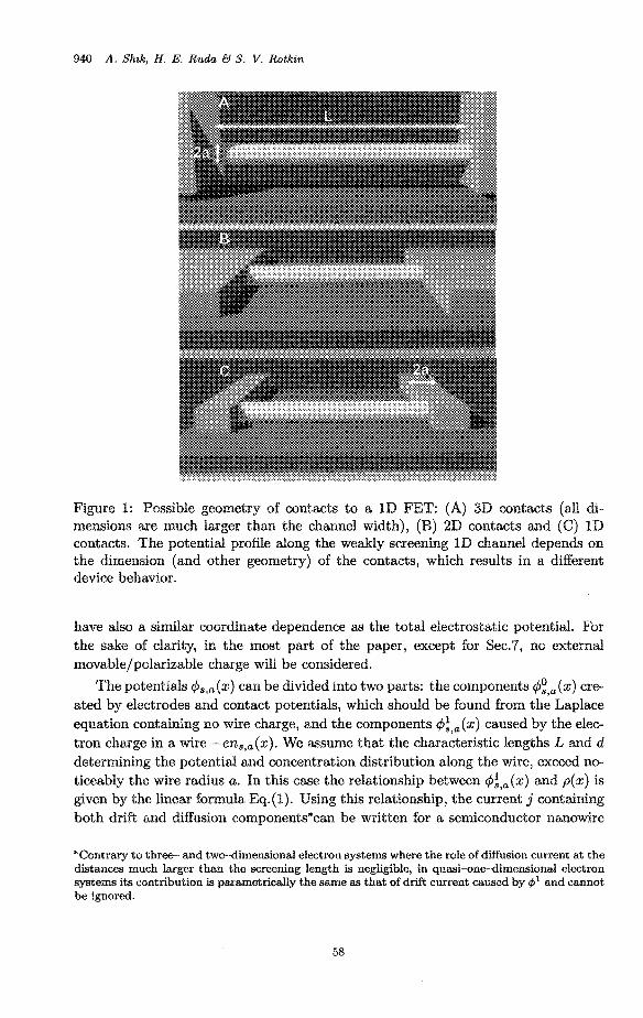
940 A. Shak, H. E. Ruda d S. V. Rotkzn
Figure 1: Possible geometry of contacts to a ID FET: (A) 3%) contacts (d1 di- mensions are much larger than the channel width), (B) 2D contacts and (C) 1D contacts. The potential profile along the weakly screening ID channel depends on the dimension (and other geometry) of the contacts, which results in a different device behavior.
have also a similar coordinate dependence as the total electrostatic potentid. For the sake of clarity, in the most part of the paper, except for Sec.7, no external movab~e/polarizable charge will be considered.
can be divided into two parts: the components c#f,,(z) ere- ated by electrodes and contact potentials, which should be found from the Laplace equation containing no wire charge, and the components +f,,(z) caused by the elec- tron charge in a wise -en,,,(z). We amume that the characteristic lengths L and d determining the potentid and concentration distribution along the wire, exceed no- ticeably the wire radius a. In this case the relationship between $:,,(z> and p ( z ) is given. by the linear formula Eq.(1). Using this relationship, the current j containing both drift and diffusion components*can be written for a semiconductor nanowire
The potentials
'Contrary to three- and two-dimensional electron systems where the role of diffusion current at the distances much larger than the screening length is negligible, in qiiaai-one-dimensiond electron systems its contribution is parametrically the same aa that of drift current caused by Cp' and cannot be ignored.
58
Electrostatics of Nanowires and Nanotubes 941
with non-degenerate carriers in the form lo:
where n = n, + n,, 4' = 4: + &, p is the carrier mobility, and the characteristic length of charge variation along the wire I in our case has the order of min{L, 2d). For a nanotube with N = 0 and degenerate carriers, k T should be replaced by the concentration-dependent Fermi energy and, instead of Eq.(2), we have ' 'v'~:
j d4O dn - = n(x)- - eC~ln(x) - - , eP dx dx (3)
where CF' is the inverse capacitance of the nanotube derived in l1 and containing both logarithmic geometrical capacitance similar to Eq. (2) and the quantum capac- itance of the 1D electron gas, l/(e2v) 0.31 for one degenerate subband of a single wall nanotube with the density of states v.
Eq.(3) is easier to solve than Eq.(2) and in this connection it is important to note that at some conditions the latter can be also reduced to a simpler form. It can be easily shown that at A = (2e2N/&kT) In ( I / a ) >> 1 the last term in Eq.(2) can be neglected and it acquires the form of Eq.(3) with C;' = ( 2 / ~ ) In ( l / a ) . This has a rather simple explanation. Two terms in the square brackets in Eq.(2) correspond, respectively, to drift in a self-consistent electric field and to diffusion. In degenerate nanotubes these terms have exactly the same appearance and may be written as a single term with the coefficient C;'. In a non-degenerate system the terms are different but for A >> 1 the diffusion term can be neglected.
We will solve the first order differential equation for n(x) given by Eq.(2) or (3), with the boundary conditions
n( fL/2) = n, (4)
assuming the source and drain to support constant concentration at the contacts, independent of the applied voltage. The two conditions Eq.(4) allow us to deter- mine the integration constant and the value of current j so far considered as some unknown constant.
Depending on the relationship between n, and N , three possible situations can be realized. The condition n, = N corresponds to ideal Ohmic contacts not disturbing electric properties of a wire, n, > N describes the situation where the carriers are provided by electrodes, which is often the case for nanotubes, and n, < N corresponds to depleted Schottky contacts. In the latter case, the regions near contacts have the lowest carrier concentration and determine the current through the structure. At the same time, this concentration is fixed by Eq.(4) and does not depend on V,. As a result, for the structures adequately described by the classical drift-diffusion theory (see Eq.(2)), transconductance will be very small. The only possible situation of an applied interest is that when the Schottky barrier has a
59
942 A. Shik, H . E. Ruda €4 S. V. Rotkin
noticeable tunnel transparency strongly dependent on V,. This situation has been thoroughly considered in 8913 and will not be discussed below.
3. Potential profile: 3D bulk electrodes
The first step in calculating characteristics of a particular FET consists in finding the potential profile 4'(x) along the channel. For n, = N it can be done by direct solution of the Laplace equation determining the potential a(., y) created by the given system of electrodes! However, for n, # N the basic formulae of the previous section require some modification. In the closest vicinity of contacts there exists a finite charge density e(N-n,) in a wire. To provide equipotentiality of metallic con- tacts, we must assume the presence of charges of the opposite sign (image charges) just beyond the contacts. This means discontinuity of charge density at x = f L / 2 and makes doubtful the adequacy of Eq.(1) assuming smooth charge and potential variations. To avoid this difficulty, we will measure n from n, by assuming in Eq.(2) n(x) = n, + An(x) . In this case, the boundary conditions Eq.(4) are replaced by
An( fL l2 ) = 0 ( 5 )
but the potential acquires an additional term q5,(x):
4%) = 4C(.> + 4&) ( 6 )
where 4,(x), as earlier, is determined by the gate, source and drain electrodes at V d = 0 while &(x) is a potential of a wire with uniform charge e(N - n,) between metallic contacts at x = fL /2 . This is just the charge which, together with its images, may have discontinuities at the contacts.
In this section we calculate ~O(Z) for the case of bulk contacts representing metallic or heavily doped semiconductor regions with all three dimensions consid- erably exceeding the characteristic lengths a, d and L. In this case the contact size can be assumed infinite as it is shown in Fig.lA. Exact calculations are rather cum- bersome and to obtain relatively simple analytical results, we make some additional approximation. Let us assume that the relation d << L, often realized in 1D FETs, is fulfilled in our system as well. In this case the potential distribution in the most part of inter-electrode space will not noticeably change if we neglect the dielectric- filled slit of the thickness d between the channel and the gate. In other words, we solve the Laplace equation A@ = 0 in the semi-infinite strip -L/2 < x < L/2; y > 0 with the boundary conditions: @(y = 0) = V,; @(x = f L / 2 ) = fVd /2 and then, assuming y = d and adding the expression for $,(x)derived in lo1 obtain the following formulae for +:,a(x):
t Here and henceforth @(z, y) represents the complete solution of the Laplace equation whereas d(z) = @(z, d ) is the potential along the wire.
60
Ekctrostatics of Nanowires and Nanotubes 943
where KO and K1 are Bessel functions of an imaginary argument 14.
4. Linear conductivity and transconductance
Now we can calculate the carrier concentration An and the electric current j caused by the driving voltage Vd. The problem is relatively simple if we restrict ourselves to the linear case by assuming V d to be sufficiently small. In the zeroth approximation j = 0 and both $O(z ) and n(x) contain only a symmetric component and are the same as in equilibrium: &(x) = &(x) + c ) ~ ( x ) , n,(x) = n, + Ano(x) where the equation for Ano(z) is:
[n, + Ano(x)] + dx (9)
Direct integration of Eq.( 9) with the boundary conditions Eq.(5) transforms it into an algebraic equation for Ano:
For degenerate carriers in a nanotube (or for A >> l), the problem is much simpler since, according to Eq.(3), Ano(x) is proportional to &(x):
Ano(x) = Ct&(X). (11)
We emphasize that Eqs.( 2),(3) were derived in the drift-diffusion approximation. On the contrary, the expressions of this section, being equilibrium, remain adequate beyond the drift-diffusion model.
To the first order in V d , the differential equations (2),(3) can be linearized in n,. The equation for a nanowire reads as:
[: In (;) [n, + Ano(x)] + e dx d4: j = [n, + Ano(x)]- - -. dx ep
61
944 A. Shik, H. E. Ruda €4 S. V. Rotkin
Since &(z) is proportional to Vd, both n,(z) and j are also h e a r in v d . Eq.(12), being solved with the conditions n,(O) = na(L/2) = 0, gives the current-induced change of concentration profile n,(x) and the implicit expression for the current j :
[[n, + Ano(x)]% - &] dx kT = o .
(13)
2e 7 In (:) [a, + $ In (k) [n, + Ano(x)] 3- e
. . The resulting j depends on the gate voltage V, through the functions @ ( x ) and Ano(x), which allows us to calculate the transistor transconductance s = dj/dV,.
For A >> 1 the problem is essentially simplified and, as it has been already mentioned, this case coincides with that for a degenerate nanotube. Instead of Eq.(12), we have:
which gives us directly
The last expression is the ordinary Kirchhoff's law, which is not surprising since the condition A >> 1 is equivalent to neglection the diffusion component of current. Taking into account Eq.(ll), we can re-write the last expression in terms of the dimensionless channel conductance cr = jL/(n,epVd):
where
and for n, = N ,
1
The a(g) dependence has a cut-off voltage go = -Q-'(O) characterized by van- ishing cr and strong increase of da/dg to the right of go. The exact behavior of these characteristics near the cut-off can be calculated analytically. They are determined by the point of minimal equilibrium concentration, which in a symmetric structure
62
Electrostatics of Nanowires and Nanotubes 945
is z = 0, and hence by the properties of 9(t) at small t . It can be easily shown that in this region 9(t) 11 n/2-arctan[exp(-nd/L)]-(n2t2/2) sinh(nd/L)/ cosh2(nd/L), which allows us to perform integration in Eq.(17) and obtain
1 n/2 - arctan[exp(nd/L)] ' go = -
Thus the transconductance s = da/dg diverges at the cut-off - (g - go)-1/2. If n, # N , the result given by Eq.(20) will not change qualitatively. In this
case the function 8 ( t ) contains additional contribution from &(z). This function, studied in more detail in lo, behaves non-analytically at z -+ f L / 2 but, similarly to 4,(z), has an extremum at 2 = 0 and can be expanded in this point. This modifies the value of go and the coefficient in a but retains unchanged the square- root character of a(g) and the divergence of s.
is equivalent to the limit of zero temperature. The resulting carrier distribution Eq.(11) does not take into account activation processes and simply gives n, = 0 for all points where &(z) < -CF1nc. The potential 4: and the carrier concentration acquire their minimal values at z = 0 and, hence, in the linear approximation, the cut-off voltage go corresponds to the condition @(O) = -C;lnc and at lower g the current is exactly zero. At non-zero temperatures the current at g < go will have an activation character because of thermal tails of the carrier distribution function: j N exp(-A/W) where A = e (-CF1nc - $: (O) ) is the barrier height. Since & ( O ) depends linearly on V, (see, for instance, Eq.(7)), the activation energy A is directly proportional to go - g. This means, in turn, that the above-mentioned singularity of da/dg is fictitious. In fact, its g-dependence will have some maximum at go with a sharp, temperature-dependent decrease at lower g. We do not consider here a tunnelling, though this effect may be important, especially if the carrier effective mass is small, as in the case of a single-wall nanotube. The tunnelling is easily in- cluded in a Wentzel-Kramers-Brilloin approximation l5 (details of the calculation for single-wall nanotubes can be found elsewhere 16).
The simplified expressions Eqs.(ll),(l4),(l6),(17) neglected diffusion effects, which
5. Current-voltage characteristic of the channel
So far we have dealt with the linear channel conductivity and transconductance at a low source-drain voltage Vd. Another important FET characteristic - the channel current-voltage characteristic (IVC) - and its dependence on the gate voltage and the temperature, can be obtained only by a numerical solution of the Eqs.(2),(3). It is convenient to use dimensionless variables measuring concentrations in units of n,, lengths in units of L, potentials in units of en,/& and current in units of e2nzp/(L&). The new dimensionless gate potential is related to the parameter g introduced in
63
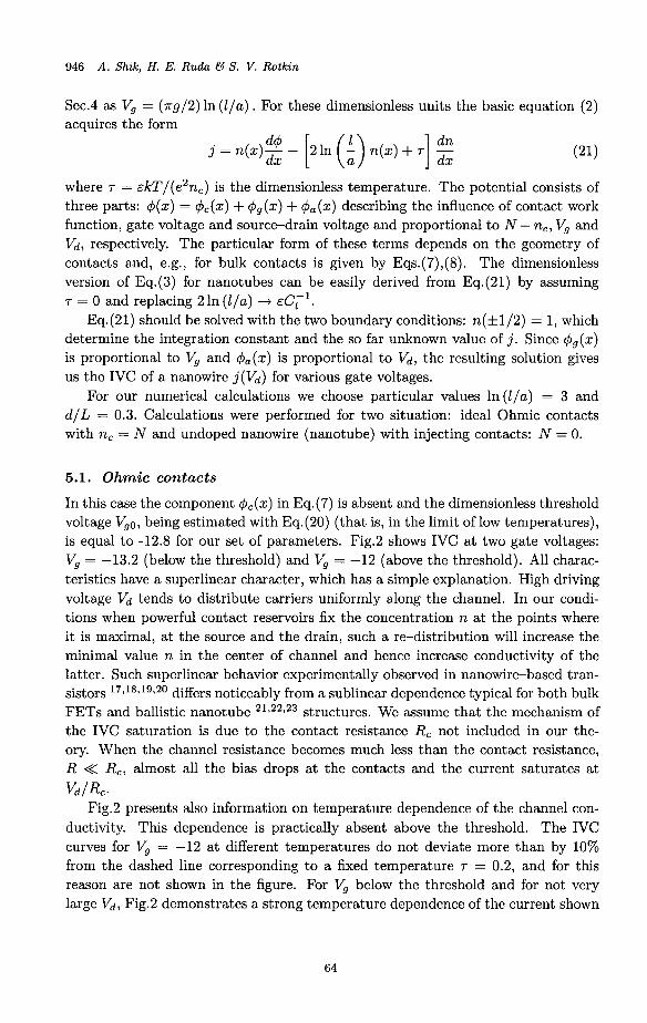
946 A . Shik, H. E. Ruda €4 S. V. Rotkin
Sec.4 as V, = (7rg/2) In ( l / a ) . For these dimensionless units the basic equation (2) acquires the form
where T = &lcT/(e2n,) is the dimensionless temperature. The potential consists of three parts: $(x) = $,(x) + $,(x) + &(x) describing the influence of contact work function, gate voltage and source-drain voltage and proportional to N - n,, V, and vd, respectively. The particular form of these terms depends on the geometry of contacts and, e.g., for bulk contacts is given by Eqs.(7),(8). The dimensionless version of Eq.(3) for nanotubes can be easily derived from Eq.(21) by assuming T = 0 and replacing 2 In ( l / a ) -+ ECF'.
Eq.(21) should be solved with the two boundary conditions: n(f1/2) = 1, which determine the integration constant and the so far unknown value of j . Since $,(x) is proportional to V, and &(x) is proportional to Vd, the resulting solution gives us the I v c of a nanowire j ( v d ) for various gate Voltages.
For our numerical calculations we choose particular values ln(l/a) = 3 and d/L = 0.3. Calculations were performed for two situation: ideal Ohmic contacts with n, = N and undoped nanowire (nanotube) with injecting contacts: N = 0.
5.1. Ohmic contacts
In this case the component q5,(x) in Eq.(7) is absent and the dimensionless threshold voltage V,O, being estimated with Eq.(20) (that is, in the limit of low temperatures), is equal to -12.8 for our set of parameters. Fig.2 shows IVC at two gate voltages: V, = -13.2 (below the threshold) and V, = -12 (above the threshold). All charac- teristics have a superlinear character, which has a simple explanation. High driving voltage Vd tends to distribute carriers uniformly along the channel. In our condi- tions when powerful contact reservoirs fix the concentration n at the points where it is maximal, at the source and the drain, such a re-distribution will increase the minimal value n in the center of channel and hence increase conductivity of the latter. Such superlinear behavior experimentally observed in nanowire-based tran- sistors 17 ,18119120 differs noticeably from a sublinear dependence typical for both bulk FETs and ballistic nanotube 21322t23 structures. We assume that the mechanism of the IVC saturation is due to the contact resistance R, not included in our the- ory. When the channel resistance becomes much less than the contact resistance, R << R,, almost all the bias drops at the contacts and the current saturates at
Fig.2 presents also information on temperature dependence of the channel con- ductivity. This dependence is practically absent above the threshold. The IVC curves for V, = -12 at different temperatures do not deviate more than by 10% from the dashed line corresponding to a fixed temperature 7 = 0.2, and for this reason are not shown in the figure. For V, below the threshold and for not very large v d , Fig.2 demonstrates a strong temperature dependence of the current shown
VdIRc.
64
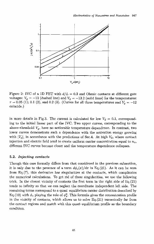
Electrostatics of Nanowires and Nanotubes 947
1
0.01
Figure 2: IVC of a 1D FET with d / L = 0.3 and Ohmic contacts at different gate voltages: V, = -12 (dashed line) and V, = -13.2 (solid lines) for the temperatures: T = 0.05 (1); 0.1 (2), and 0.2 (3). (Curves for all three temperatures and V, = -12 coincide.)
in more details in Fig.3. The current is calculated for low V d = 0.1, correspond- ing to the initial linear part of the IVC. Two upper curves, corresponding to the above-threshold V,, have no noticeable temperature dependence. In contrast, two lower curves demonstrate such a dependence with the activation energy growing with lVgl, in accordance with the predictions of Sec.4. At high V d , where contact injection and electric field tend to create uniform carrier concentration equal to nc, different IVC curves become closer and the temperature dependence collapses.
5.2. Injecting contacts
Though this case formally differs from that considered in the previous subsection, it is only due to the presence of a term d&(z)/da: in Eq.(21). As it can be seen from Eq.(7), this derivative has singularities at the contacts, which complicates the numerical calculations. To get rid of these singularities, we use the following trick. In the closest vicinity of contacts the first term in the right side of Eq.(21) tends to infinity so that we can neglect the coordinateindependent left side. The remaining terms correspond to a quasi-equilibrium carrier distribution described by Eq.(lO) with # J ~ playing the role of &. This formula gives the concentration profile in the vicinity of contacts, which allows us to solve Eq.(21) numerically far from the contact regions and match with this quasi-equilibrium profile as the boundary condition.
65
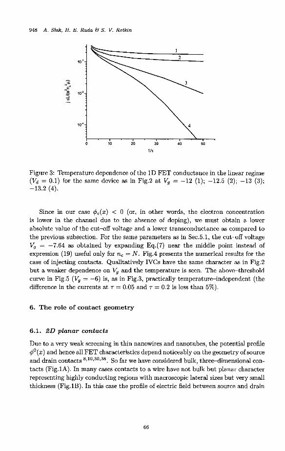
948 A . Shik, H. E. Ruda €4 S. V. Rotkin
Figure 3: Temperature dependence of the 1D FET conductance in the linear regime (Vd = 0.1) for the same device as in Fig.2 at V, = -12 (1); -12.5 (2); -13 (3); -13.2 (4).
Since in our case $c(lc) < 0 (or, in other words, the electron concentration is lower in the channel due to the absence of doping), we must obtain a lower absolute value of the cut-off voltage and a lower transconductance as compared to the previous subsection. For the same parameters as in Sec.5.1, the cut-off voltage V, = -7.64 as obtained by expanding Eq.(7) near the middle point instead of expression (19) useful only for nc = N . Fig.4 presents the numerical results for the case of injecting contacts. Qualitatively IVCs have the same character as in Fig.2 but a weaker dependence on V, and the temperature is seen. The abovethreshold curve in Fig.5 (V, = -6) is, as in Fig.3, practically temperature-independent (the difference in the currents at T = 0.05 and T = 0.2 is less than 5%).
6. The role of contact geometry
6.1. 2D planar contacts
Due to a very weak screening in thin nanowires and nanotubes, the potential profile $ O ( l c ) and hence all FET characteristics depend noticeably on the geometry of source and drain contacts 8910 ,30v38 . So far we have considered bulk, three-dimensional con- tacts (Fig.lA). In many cases contacts to a wire have not bulk but planar character representing highly conducting regions with macroscopic lateral sizes but very small thickness (Fig.lB). In this case the profile of electric field between source and drain
66
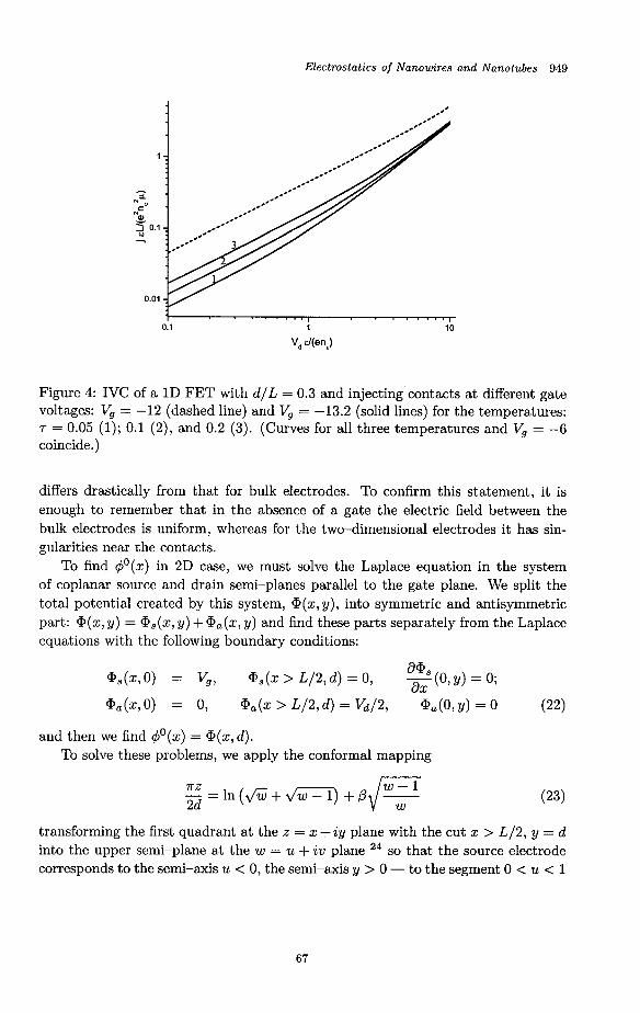
Electrostatics of Nanowires and Nanotubes 949
1 1 I
v, 4 e n J 0.1 1 10
Figure 4: IVC of a 1D FET with d / L = 0.3 and injecting contacts at different gate voltages: V, = -12 (dashed line) and V, = -13.2 (solid lines) for the temperatures: T = 0.05 (1); 0.1 (2), and 0.2 (3). (Curves for all three temperatures and V, = -6 coincide.)
differs drastically from that for bulk electrodes. To confirm this statement, it is enough to remember that in the absence of a gate the electric field between the bulk electrodes is uniform, whereas for the two-dimensional electrodes it has sin- gularities near the contacts.
To find 4O(x) in 2D case, we must solve the Laplace equation in the system of coplanar source and drain semi-planes parallel to the gate plane. We split the total potential created by this system, @(x, y), into symmetric and antisymmetric part: @(x, y) = aS(x, y) + a a ( x , y) and find these parts separately from the Laplace equations with the following boundary conditions:
a@., ax @,(x,O) = V,, QS(z > L/2,d) = 0, -(O,y) = 0;
@ a ( ~ , 0) = 0, @,(a: > L/2, d ) = V d / 2 , @a(O, y) = 0 (22)
and then we find +O(x) = @(x, d). To solve these problems, we apply the conformal mapping
transforming the first quadrant at the z = x + iy plane with the cut x > L/2, y = d into the upper semi-plane at the w = u + iv plane 24 so that the source electrode corresponds to the semi-axis u < 0, the semi-axis y > 0 - to the segment 0 < u < 1
67
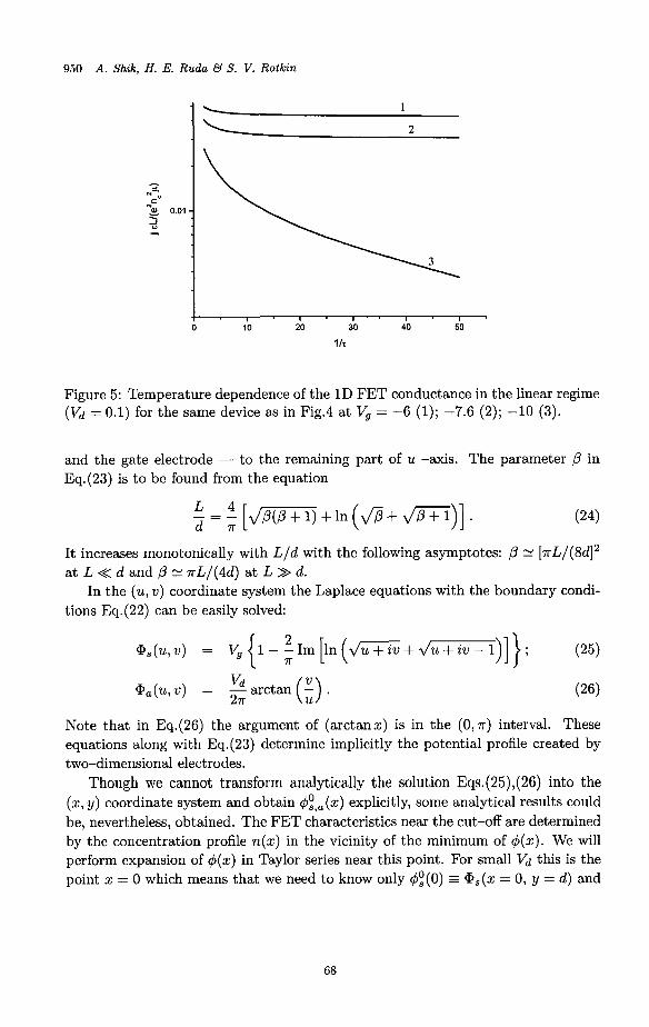
950 A . Shik, H. E. Ruda d S. V. Rotkin
1
2
Figure 5: Temperature dependence of the 1D FET conductance in the linear regime (vd = 0.1) for the same device as in Fig.4 at V, = -6 (1); -7.6 (2); -10 (3).
and the gate electrode - to the remaining part of u -axis. The parameter ,B in Eq.(23) is to be found from the equation
(24) - = - [ d r n + I n ( d P + r n ) ] . L 4 d r
It increases monotonically with L/d with the following asymptotes: ,B 2~ [7rL/(8dI2 at L << d and ,B N 7rL/(4d) at L >> d.
In the (u, w) coordinate system the Laplace equations with the boundary condi- tions Eq.(22) can be easily solved:
Note that in Eq.(26) the argument of (arctanz) is in the ( 0 , ~ ) interval. These equations along with Eq. (23) determine implicitly the potential profile created by two-dimensional electrodes.
Though we cannot transform analytically the solution Eqs.(25),(26) into the (z, y) coordinate system and obtain q5:,a(z) explicitly, some analytical results could be, nevertheless, obtained. The FET characteristics near the cut-off are determined by the concentration profile n(z) in the vicinity of the minimum of q5(z). We will perform expansion of $(z) in Taylor series near this point. For small v d this is the point 5 = 0 which means that we need to know only &(O) = QS(z = 0, y = d) and
68
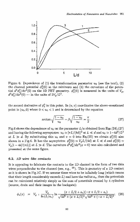
Electrostatics of Nanowires and Nanotubes 951
0 10 Lld
5
Figure 6: Dependence of (1) the transformation parameter uo (see the text), (2) the channel potential @(O) at the minimum and (3) the curvature of the poten- tial d2&/dx2(0 ) on the 1D FET geometry. &(O) is measured in the units of V,, d2&/dx2(0 ) - in the units of 2V,/L2.
the second derivative of &’ in this point. In (ul v) coordinates the abovementioned point is (UO, 0) where 0 < uo < 1 and is determined by the equation
Fig.6 shows the dependence of uo on the parameter L/a obtained from Eqs.(24),(27) and having the following asymptotes: uo N [7rL/(8d)I2 at L << d and uo 2~ 1-4d2/L2 at L >> d. By substituting this uo and v = 0 into Eq.(25) we obtain &(O) also shown in a Fig.6. It has the asymptotes: &(O) 21 VgL/(4d) at L << d and &(O) N
V,[1 - 4d/(rL)] at L >> d. The curvature d2&/dx2(x = 0) was also calculated and presented at the same figure.
6.2. 1D wire-like contacts
It is appealing to fabricate the contacts to the 1D channel in the form of two thin wires perpendicular to the channel (see, e.g., ”)). This is geometry of a 1D contact as it is shown in Fig.lC. If we assume these wires to be infinitely long (which means that their length considerably exceeds L) and have the radius a,, then the potentials can be calculated relatively simply as the sum of potentials created by 4 cylinders (source, drain and their images in the backgate):
(x + L/2 + + L/2 + . (28) In ‘s(x) = vg + In (L/a,) ,/4d2 + (x + L/2)2,/4d2 + (-x + L/2)2’
69
952 A . Shik, H. E. Ruda l3 S. V. Rotkin
(29) (-2 + L/2 + a,) d4d2 + (x + L/2)2
(--2 + L/2 + a,) d4d2 + ( --2 + L/2)2 ' In -
' a ( -2 ) - 2 In ( L / ~ c )
Calculations of the transconductance in the linear regime are based on the same formula Eq.(17) as in the Sec.4. The quantitative difference is in a particular profile of the q(t) function. Though its expansion near the maximum is, of course, also quadratic and hence it gives qualitatively the same final result di/dg = A(g - go)-1/2, the expansion coefficients are different. As a result, the cut-off voltage go and the coefficient A may differ considerably from the case of bulk contacts. The whole IVC, as before, must be found by numerical calculations taking into account the fact that for twedimensional contacts not only q5,(-2) but also ',(-2)
have singularities near the contacts. Thus one has to match the numerical solution in the middle of the channel with an analytical quasi-equilibrium solution in the region near the contacts as described in Sec.5.2, even for the Ohmic contacts.
7. Hysteresis and memory effects
The theoretical model considered in the previous sections gives a general physical picture and qualitative regularities describing electrical parameters of 1D FETs but, being general, cannot account for all specific features observed experimentally. For instance, some recent studies 2 6 9 2 7 3 2 8 demonstrated that IVCs of nanotube-based FETs have a strong hysteretic effect revealed as a difference in the threshold gate voltages measured for V, swept in positive and negative direction. A similar hys- teresis is known to exist for Si devices and exploited for the memory elements 29. By analogy, it was supposed that these nanotube FETs may also become nonvolatile memory elements operating at the few-(sing1e)electron level even at elevated tem- peratures. In Si devices hysteresis is usually explained by generation/recombination of electrons at the traps in the oxide layer (the so-called slow surface states). In our case, we may expect a similar recharging stimulated by the channel-gate elec- tric field (the Fowler-Nordheim effect). This field in quasi-1D-systems is - a-1 in the vicinity of channel and, hence, can be very high. One may therefore expect the memory effects to be observed at lower V,, as compared to classical FETs. The described electron tunnelling to (or from) dielectric layer causes potential re- distribution in the system resulting in a shift of the threshold voltage. Due to a low tunnelling probability, the characteristics time of corresponding charge trans- port may exceed the inverse frequency of V, sweeping, which is consistent with the observed hysteresis.
For further phenomenological description we assume that the distribution of this charge is cylindrically symmetric. For FET model with a cylindrical gate (see, e.g., 30) it is definitely the case. Moreover, we may expect this assumption to be also correct even in the planar gate geometry discussed in the previous sections if the nanotube/nanowire is completely buried in the oxide. According to the general ex- pressions of Sec.2, we can claim that the shift of threshold voltage due to recharging of traps in the dielectric
70
Electrostatics of Nanowires and Nanotubes 953
eSN(0) SVyJ = - ct ’ where SN(0) is the linear density of such charged traps taken at x = 0 since this point plays the role of a ’bottleneck’ determining the offset of channel current.
The value of SN(0) is found from the generation-recombination equation de- scribing recharging of traps through the Fowler-Nordheim mechanism. If the max- imal possible SN(0) is limited by the total density of empty traps in a thin shell accessible for tunnelling electron, No,khen its dynamics is dictated by the equation
dSN(0) JCT -- - - [No - SN(O)] . d t e
Here CT = 10-17cm2 is the cross-section of the generation (and recombination) 31,
and we estimate N ( 0 ) = 1013 cm-2 33 . The Fowler-Nordheim current density depends on the electric field near the FET channel E , which in turn depends on the potential and the radius of the 1D channel R (and logarithmically depends on the gate distance d) : E = 4/(Rln(d/2R)).
J = A42 exp(-B/4) (32)
where the constants A N lo5 A cm-2V-2 and B N 150V are known for tunnelling in typical materials 32 and depend mostly on the effective mass of the carriers and the trap level.
Eq.(32) has been solved numerically and the result depends on the sweeping rate (SR) and the sweeping range of V, that reflect the specifics of a particular experiment with a nanotube or nanowire FET. The physics of this dependence is clear: the slower V, is swept and the larger is the sweeping range, the larger the density of injected electrons (cumulative charge in the substrate in our case), and thus the larger the hysteresis in accord with Eq.(30). The results of our modelling are presented in Fig.7. The potential of the ionized impurities creates an additional term (30) in the external potential as given by Eq.(7). This term is plotted in the figure as a function of the gate voltage. This extra term shifts the threshold voltage as given by expression (20). The shift is different for different direction of the gate voltage sweep, because the traps are charged/discharged when the voltage is swept up/down.
The dependence of the hysteresis width, H , on the sweeping rate is close to logarithmic. We explain this by the exponential dependence of the steady state solution of the Eqs. (31,32) on the electrostatic potential, then, the potential itself is roughly proportional to the log SN which is proportional in turn to the sweeping rate. Similarly, the hysteresis increases with the sweeping range as shown in Fig.8.
$For large No, the maximal SN(0) can be limited not by the absence of empty traps but by the drop of the local channel-gate electric field making the tunnelling rate too small to be observed in real time.
71
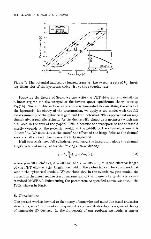
954 A . Shik, H. E. Ruda €4 S. V. Rotkin
10, I
2
Gate voltage (V)
Figure 7: The potential induced by ionized traps vs. the sweeping rate of V,. Inset: log-linear plot of the hysteresis width, H , vs the sweeping rate.
Following the theory of Sec.4, we can write the FET drive current density in a linear regime via the integral of the inverse quasi-equilibrium charge density, Eq.(16). Since in this section we are mostly interested in describing the effect of the hysteresis, for clarity of the presentation, we apply a toy model with the full axial symmetry of the cylindrical gate and trap potential. This approximation may though give a realistic estimate for the device with planar gate geometry which was discussed in the rest of the paper. This is because the transport at the threshold mostly depends on the potential profile at the middle of the channel, where it is almost flat. We note that in this model the effects of the fringe fields at the channel ends and all contact phenomena are fully neglected.
If all potentials have full cylindrical symmetry, the integration along the channel length is trivial and gives for the driving current density:
(33) w L j = Vd-(n, + Ano(z)).
where p = 9000 cm2/Vs, d = 500 nm and L = 10d = 5pm is the effective length of the FET channel (the length over which the potential can be considered flat within the cylindrical model). We conclude that in the cylindrical gate model, the current in the linear regime is a linear function of the channel charge density as in a standard MOSFET. Substituting the parameters as specified above, we obtain the IVCs, shown in Fig.9.
8. Conclusions
The present work is devoted to the theory of nanowire and nanotube based transistor structures, which represents an important step towards developing a general theory of nanoscale 1D devices. In the framework of our problem we model a carrier
72
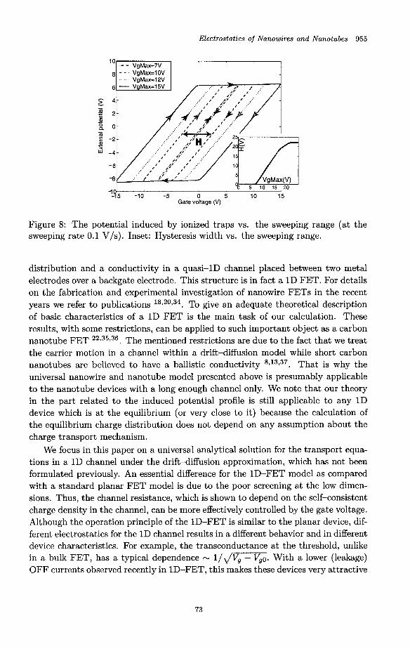
Electrostatics of Nanowires and Nanotubes 955
Figure 8: The potential induced by ionized traps vs. the sweeping range (at the sweeping rate 0.1 V/s). Inset: Hysteresis width vs. the sweeping range.
distribution and a conductivity in a quasi-1D channel placed between two metal electrodes over a backgate electrode. This structure is in fact a 1D FET. For details on the fabrication and experimental investigation of nanowire FETs in the recent years we refer to publications 18120134. To give an adequate theoretical description of basic characteristics of a 1D FET is the main task of our calculation. These results, with some restrictions, can be applied to such important object as a carbon nanotube FET 22,35,36. The mentioned restrictions are due to the fact that we treat the carrier motion in a channel within a drift-diffusion model while short carbon nanotubes are believed to have a ballistic conductivity s , 1 3 7 3 7 . That is why the universal nanowire and nanotube model presented above is presumably applicable to the nanotube devices with a long enough channel only. We note that our theory in the part related to the induced potential profile is still applicable to any 1D device which is at the equilibrium (or very close to it) because the calculation of the equilibrium charge distribution does not depend on any assumption about the charge transport mechanism.
We focus in this paper on a universal analytical solution for the transport equa- tions in a 1D channel under the drift-diffusion approximation, which has not been formulated previously. An essential difference for the 1D-FET model as compared with a standard planar FET model is due to the poor screening at the low dimen- sions. Thus, the channel resistance, which is shown to depend on the self-consistent charge density in the channel, can be more effectively controlled by the gate voltage. Although the operation principle of the 1D-FET is similar to the planar device, dif- ferent electrostatics for the 1D channel results in a different behavior and in different device characteristics. For example, the transconductance at the threshold, unlike in a bulk FET, has a typical dependence - 1/,/-. With a lower (leakage) OFF currents observed recently in 1D-FET, this makes these devices very attractive
73
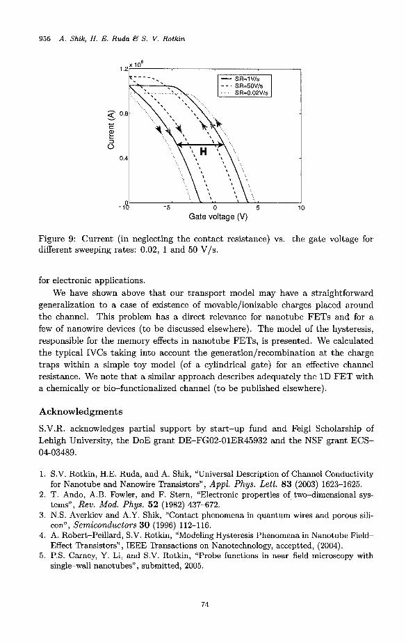
956 A . Shik, H. E. Ruda €d S. V. Rotkin
x lo8 1.2,
Gate voltage (V)
Figure 9: Current (in neglecting the contact resistance) vs. the gate voltage for different sweeping rates: 0.02, 1 and 50 V/s.
for electronic applications. We have shown above that our transport model may have a straightforward
generalization to a case of existence of movable/ionizable charges placed around the channel. This problem has a direct relevance for nanotube FETs and for a few of nanowire devices (to be discussed elsewhere). The model of the hysteresis, responsible for the memory effects in nanotube FETs, is presented. We calculated the typical IVCs taking into account the generation/recombination at the charge traps within a simple toy model (of a cylindrical gate) for an effective channel resistance. We note that a similar approach describes adequately the 1D FET with a chemically or bio-functionalized channel (to be published elsewhere).
Acknowledgments
S.V.R. acknowledges partial support by start-up fund and Feigl Scholarship of Lehigh University, the DOE grant DE-FG02-01ER45932 and the NSF grant ECS- 04-03489.
1. S.V. Rotkin, H.E. Ruda, and A. Shik, “Universal Description of Channel Conductivity
2. T. Ando, A.B. Fowler, and F. Stern, “Electronic properties of two-dimensional sys-
3. N.S. Averkiev and A.Y. Shik, “Contact phenomena in quantum wires and porous sili-
4. A. Robert-Peillard, S.V. Rotkin, “Modeling Hysteresis Phenomena in Nanotube Field-
5. P.S. Carney, Y. Li, and S.V. Rotkin, “Probe functions in near-field microscopy with
for Nanotube and Nanowire Transistors” Appl. Phys. Lett. 83 (2003) 1623-1625.
tems”, Rev. Mod. Phys. 52 (1982) 437-672.
con”, Semiconductors 30 (1996) 112-116.
Effect Transistors”, IEEE Transactions on Nanotechnology, acceptted, (2004).
single-wall nanotubes” , submitted, 2005.
74
Electrostatics of Nanowires and Nanotubes 957
6. S.V. Rotkin, “Theory of Nanotube Nanodevices”, in Nanostructured Materials and Coatings for Biomedical and Sensor Applications, (Proceedings of the NATO Ad- vanced Research Workshop; August 4-8, 2002, Kiev, Ukraine). Editors: Y.G. Gogotsi and Irina V. Uvarova. Kluwer Academic Publishers: Dordrecht-Boston-London. NATO Science Series: 11. Mathematics, Physics and Chemistry - Vol. 102, pp. 257-277, (2003).
7. D. Lu, Y. Li, S.V. Rotkin, U. Ravaioli, and K. Schulten, “Wall Polarization in a Carbon Nanotube Water Channel”, Nan0 Lett., 4(12), (2004) 2383-2387. For an experimental work, see N. Naguib, H. Ye, Y. Gogotsi, A.G. Yazicioglu, C.M. Megaridis, and M. Yoshimura, “Observation of Water Confined in Nanometer Channels of Closed Carbon Nanotubes” Nan0 Lett., 4(11), (2004) 2237-2243.
8. S. Heinze, J. Tersoff, R. Martel, V. Derycke, J. Appenzeller, and Ph. Avouris, “Car- bon Nanotubes as Schottky Barrier Transistors” Phys. Rev. Lett. 89 (2002) 106801- 106804.
9. A.G. Petrov, S.V. Rotkin, ‘Transport in Nanotubes: Effect of Remote Impurity Scat- tering”, Phys. Rev. B vol. 70 no. 3 (2004) 035408-1-10.
10. H. Ruda and A. Shik, “Influence of contacts on the conductivity of thin wires”, J.
11. K.A. Bulashevich and S.V. Rotkin, “Nanotube Devices: Microscopic Model”, JETP Lett. 75(2002) 205-209.
12. S.V. Rotkin, V. Srivastava, K.A. Bulashevich, and N.R. Aluru, “Atomistic Capacitance of a Nanotube Electromechanical Device”, Int. J. Nanosci. 1 (2002) 337-346.
13. T. Nakanishi, A. Bachtold, and C. Dekker, “Transport through the interface between a semiconducting carbon nanotube and a metal electrode”, Phys. Rev. B 66, (2002)
14. M. Abramowitz and L. Stegun, Handbook of Mathematical Functions with Formu-
15. L.D. Landau, E.M. Lifshits. Quantum Mechanics, (Pergamon, Oxford, 1984). 16. S.V. Rotkin, “Theory of Nanotube Opto-electromechanical Device” , Proceedings of
Third IEEE conference on Nanotechnology, 12-14 August 2003. Moscone Convention Center, San-Francisco, CA. pp. 631-634.
17. T. Maemoto, H. Yamamoto, M. Konami, A. Kajiuchi, T. Ikeda, S. Sasa, and M. Inoue, “High-speed quasi-one-dimensional electron transport in InAs/AlGaSb mesoscopic de- vices”, Phys. Stat. Sol. (b) 204 (1997) 255-258.
18. Y . Cui, X. Duan, J. Hu, and C. M. Lieber, “Doping and electrical transport in silicon nanowires”, J . Phys. Chem. B 104 (2000) 5213-5216.
19. G. L. Harris, P. Zhou, M. He, and J. B. Halpern, “Semiconductor and photoconduc- tive GaN nanowires and nanotubes”, Lasers and Electro-Optics, 2001, CLEO’Ol. Technical Digest, p.239.
20. J.-R. Kim, H. M. So, J. W. Park, J.-J. Kim, J. Kim, C. J. Lee, and S. C. Lyu, “Electrical transport properties of individual gallium nitride nanowires synthesized by chemical- vapor-deposition” , Appl. Phys. Lett. 80 (2002) 3548-3550.
21. X. Liu, C. Lee, and C. Zhou, “Carbon nanotube field-effect inverters”, Appl. Phys. Lett. 79 (2001) 3329-3331.
22. S. J. Wind, J. Appenzeller, R. Martel, V. Derycke, and P. Avouris, “Vertical scaling of carbon nanotube field-effect transistors using top gate electrodes”, Appl. Phys. Lett.
23. F. Leonard and J. Tersoff, “Multiple Functionality in Nanotube Transistors”, Phys.
24. W. von Koppenfels and F. Stallmann, Praxis der konformen Abbildung, (Springer-
Appl. Phys. 84 (1998) 5867-5872.
073307-073310.
las, Graphs, and Mathematical Tables, (Academic Press, 1975).
80 (2002) 3817-3819.
Rev. Lett. 88 (2002) 258302-258305.
Verlag, 1959).
75
958 A . Shik, H. E. Ruda €4 S. V. Rotkin
25. J.-F. Lin, J.P. Bird, L. Rotkina, and P.A. Bennett, “Classical and quantum transport in focused-ion-beam-deposited Pt nanointerconnects” , Appl. Phys. Lett. 82 (2003)
26. M. Radosavljevic, M. Freitag, K. V. Thadani, and A. T. Johnson, “Nonvolatile Molecu- lar Memory Elements Based on Ambipolar Nanotube Field-Effect Transistors”, Nano Letters, v.2 (2002) 761-764.
27. M. S. Fuhrer, B. M. Kim, T. Durkop, and T. Brintlinger, “High Mobility Nanotube Transistor Memory”, Nano Letters, v.2 (2002) 755-759.
28. W. Kim, A. Javey, 0. Vermesh, Q. Wang, Y. Li, and H. Dai, “Hysteresis Caused by Water Molecules in Carbon Nanotube Field-Effect Transistors”, Nano Letters, v.3
29. L. Guo, E. Leobandung, and S.Y. Chou “A Silicon Single-Electron Transistor Memory Operating at Room Temperature”, Science 275 (1997) 649-651.
30. A. Odintsov and Y . Tokura, “Contact Phenomena and Mott Transition in Carbon Nanotubes”, Journal of Low Temp. Physics, v.118, no 5-6 (2000) 509-518.
31. Y . Roh, L. Trombetta, J. Han, “Analysis of Charge Components Induced by Fowler- Nordheim Tunnel Injection in Silicon Oxides Prepared by Rapid Thermal Oxidation”, J. Electrochem. SOC., v.142 (1995) 1015-1020.
802-804.
(2003) 193-198.
32. P.T. Landsberg, Recombination in semiconductors, (Cambridge, 1991). 33. M. Fischetti, R. Gastaldi, F. Maggioni, and A. Modelli, “Positive charge effects on the
flatband voltage shift during avalanche injection on Al-Si 02-Si capacitors,” J. of Appl.
34. H. Hasegawa and S. Kasai, “Hexagonal binary decision diagram quantum logic cir- cuits using Schottky in-plane and wrapgate control of GaAs and InGaAs nanowires”, Physica E 11, no. 2-3 (2001) 149-154.
35. S. J. Tans, A. R. M. Verschueren, and C. Dekker, “Room-temperature transistor based on a single carbon nanotube” , Nature 393 (1998) 49-52.
36. R. Martel, T. Schmidt, H. R. Shea, T. Hertel, and P. Avouris, “Single- and multi-wall carbon nanotube field-effect transistors”, Appl. Phys. Lett. 73 (1998) 2447-2449.
37. J. Guo, M. Lundstrom, and S. Datta, “Performance projections for ballistic carbon nanotube field-effect transistors”, Appl. Phys. Lett. 80 (2002) 3192-3194.
38. Authors are grateful t o an Anonimous Reviewer for calling our attention to the ref- erence: J. Guo, J. Wang, E. Polizzi, s. Datta, and M. Lundstrom, “Electrostatics of nanowire transistors”, IEEE Trans. on Nanotechnology 2 (2003) 329-334, which paper further applies results of 30 and l1 to a specific device geometry.
Phys., VO~. 53 (1982) 3129-3136.
76
World Scientific www.worldscientific.com
International Journal of High Speed Electronics and Systems
@ World Scientific Publishing Company Vol. 16, NO. 4 (2006) 959-975
CARBON NANOTUBE BASED NONVOLATILE MEMORY DEVICES
WEGANG ZHANG
Intel Corporation, 2200 Mission College Boulevard, Santa Clara, CA 95054, USA
The technology progress and increasing high density demand have driven the nonvolatile memory devices into nanometer scale region. There is an urgent need of new materials to address the high programming voltage and current leakage problems in the current flash memory devices. As one of the most important nanomaterials with excellent mechanical and electronic properties, carbon nanotube has been explored for various nonvolatile memory applications. While earlier proposals of “hucky shuttle” memories and nanoelectromechanical memories remain as concepts due to fabrication difficulty, recent studies have experimentally demonstrated various prototypes of nonvolatile memory cells based on nanotube field-effect-transistor and discrete charge storage bits, which include nano-floating gate memory cells using metal nanocrystals, oxide-nitride-oxide memory stack, and more simpler trap-in-oxide memory devices. Despite of the very limited research results, distinct advantages of high charging efficiency at low operation voltage has been demonstrated. Single-electron charging effect has been observed in the nanotube memory device with quantum dot floating gates. The good memory performance even with primitive memory cells is attributed to the excellent electrostatic coupling of the unique one-dimensional nanotube channel with the floating gate and the control gate, which gives extraordinary charge sensibility and high current injection efficiency. Further improvement is expected on the retention time at room temperature and programming speed if the most advanced fabrication technology were used to make the nanotube based memory cells.
Keywords: carbon nanotube; non-volatile memory device; FET; nanocrystal; quantum dot; floating gate; single-electron charging.
1. Introduction
The rapid market expansion of personal computers and other consumer electronics such as digital cameras, mobile phones, MP3 players and personal data assistant devices, has triggered a continuing demand for nonvolatile electronic memories that are cheaper, faster, of higher storage density, and lower power consumption. For the past three decades, this has been achieved mainly by scaling of the physical dimensions of the devices following the technology roadmaps of the semiconductor industry [l]. The current technology node for flash memory, a mainstream nonvolatile memory in current market, has reached 90 nm, and is expected to scale down to 32 nm in the next couple of years. It is, however, becoming more and more difficult to continue this trend as we entered the nanoscale region due to the short channel effects in the scaling of metal-oxide-semiconductor field-effect-transistor (MOSFET) and the conflicting requirement for charging speed and retention time in the scaling of tunneling oxide. Researchers have been exploring new materials and cell structures to
77
960 Y. Zhang
overcome these difficulties and to extend the roadmap of flash memory. Discrete nanocrystal floating gate [2], crested tunneling barrier [3], oxide-nitride-oxide (ONO) stack [4,5] have been proposed to improve the tunneling efficiency and the charge retention. Ultrathin body silicon-on-insulator (SOI) [6] and FinFET [7] has been used to reduce the short channel effect and improve electrostatic coupling. Beyond the flash memory extension, researchers also started to investigate many emerging research memory devices that are not based on electronic charge storage, such as phase change, resistance change, ferroelectric, magnetic, and molecular memory [ 11.
*
Among various materials explored for non-volatile memory applications, carbon nanotube (CNT) has attracted great interest due to its unique geometry and excellent mechanical and electrical properties [8,9]. The unique features of CNTs have enabled researchers to conceive some novel memory concepts, such as shuttle memory and nanoelectromechanical memory, which do not apply to any other materials. On the other hand, those features also enabled us to explore the possibility to extend the current flash memory to its extreme limit by replacing silicon with semiconducting CNTs. This paper will give a review of different CNT memory devices that have been studied in recent years. The operation principles and experimental realization, as well as their technical merits and limitations, will be discussed. Focus will be on the carbon nanotube field-effect-transistor (CNTFET) based memory because it is the most intensively studied CNT memory device.
2. CNT shuttle memory and nanoelectromechanical memory
The first non-volatile CNT memory concept proposed is the “bucky shuttle” - a naturally ionized endohedral fullerene (also called “bucky ball”) shuttling within a bigger fullerene or nanotube [lo]. This idea is based on the unique geometry of a nanotube whose hollow inner space and closed ends define a perfect place to hold smaller molecules like a peapod [ 10,l I]. The encapsulated endohedral fullerene can reside in one of the two stable energy states at the opposite ends of the hosting nanotube and be switched between these two positions by applying an electric field as shown in Fig. 1. There is, however, no promising scheme to read the states of such memories. To resolve this problem, a new version of “nanotube shuttle” memory device has been proposed [12,13]. This device is composed of two one-side capped outer single-walled nanotubes (SWNT) with aligned open ends and an encapsulated short nanotube shuttling between them (Fig. 2). Depending on which SWNT the encapsulated nanotube resides in, the electronic property of that side will change (partially becomes double-walled) [14,15] and this will enable the detection of the memory states. The encapsulated nanotube can be formed by annealing endohedral fullerenes [16,17]. The two outer SWNTs can be made by cutting a SWNT using lithography and etching technology [ 131. The gap between the two open ends should be controlled small enough so that the encapsulated nanotube could not escape the system. Despite of the interesting theoretical simulation results, no experimental study has been done on the shuttle type CNT memories due to the difficulties to fabricate the cell itself and the electrical contacts.
78
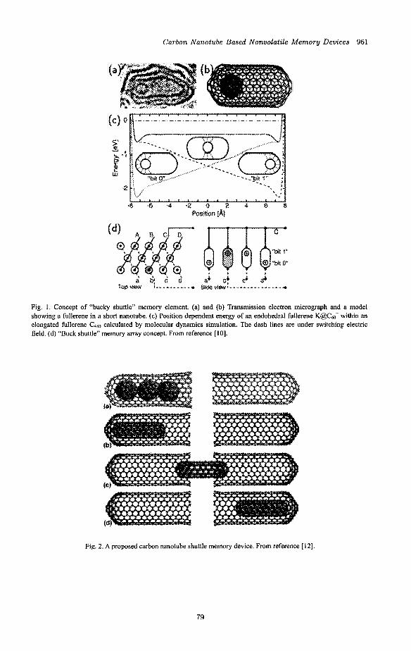
Carbon Nanotube Based Nonvolatile Memory Devices 961
Fig. 1. Concept of “bucky shuttle” memory element. (a) and (b) Transmission electron micrograph and a model showing a fullerene in a short nanotube. (c) Position dependent energy of an endohedral fullerene K@Cm’ within an elongated fullerene C480 calculated by molecular dynamics simulation. The dash lines are under switching electric field. (d) “Buck shuttle” memory array concept. From reference [lo].
Fig. 2. A proposed carbon nanotube shuttle memory device. From reference [12].
79
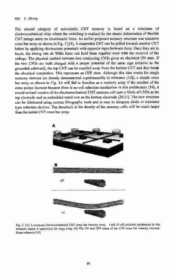
962 Y. Zhang
The second category of nonvolatile CNT memory is based on a miniature of electromechanical relay where the switching is realized by the elastic deformation of flexible CNT strings under an electrostatic force. An earlier proposed memory structure was nanotube cross bar array as shown in Fig. 3 [ 181. A suspended CNT can be pulled towards another CNT below by applying electrostatic potentials with opposite signs between them. Once they are in touch, the strong van de Walls force can hold them together even with the removal of the voltage. The physical contact between two conducting CNTs gives an electrical ON state. If the two CNTs are both charged with a proper potential of the same sign (relative to the grounded substrate), the top CNT can be repelled away from the bottom CNT and thus break the electrical connection. This represents an OFF state. Although this idea works for single memory element (as already demonstrated experimentally in reference [ 18]), a simple cross bar array as shown in Fig. 3A will fail to function as a memory array if the number of the cross points increase because there is no cell selection mechanism in this architecture [19]. A recent revised version of the electromechanical CNT memory cell uses a fabric of CNTs as the top electrode and an embedded metal row as the bottom electrode [20,21]. The new structure can be fabricated using current lithography tools and is easy to integrate diode or transistor type selection devices. The drawback is the density of the memory cells will be much larger than the initial CNT cross bar array.
Fig. 3. (A) A proposed electromechanical CNT cross bar memory array. Lack of cell selection mechanism in this structure makes it unpractical for large array. (B) The ON and OFF states of the CNT cross bar memory element. From reference [ 181.
80
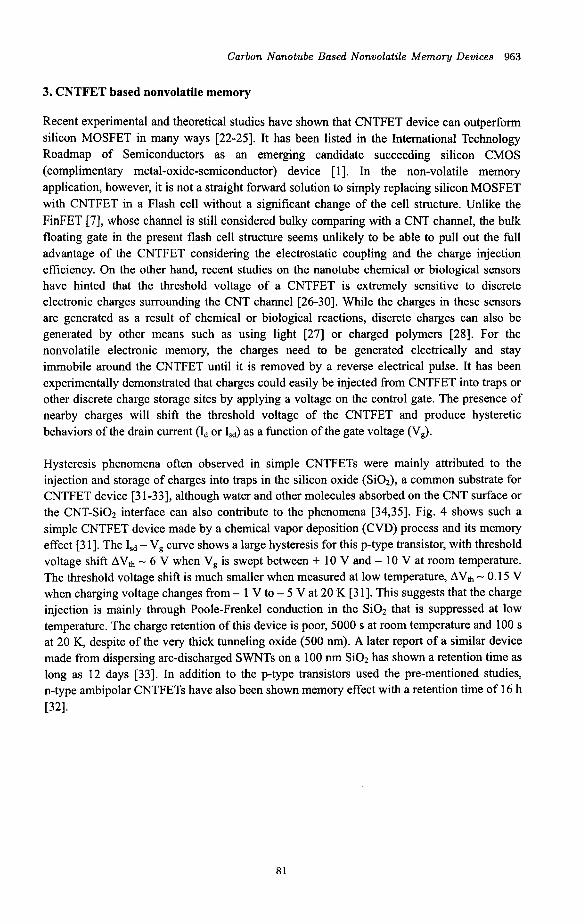
Carbon Nanotube Based Nonvolatile Memory Devices 963
3. CNTFET based nonvolatile memory
Recent experimental and theoretical studies have shown that CNTFET device can outperform silicon MOSFET in many ways [22-251. It has been listed in the International Technology Roadmap of Semiconductors as an emerging candidate succeeding silicon CMOS (complimentary metal-oxide-semiconductor) device [ 13. In the non-volatile memory application, however, it is not a straight forward solution to simply replacing silicon MOSFET with CNTFET in a Flash cell without a significant change of the cell structure. Unlike the FinFET [7], whose channel is still considered bulky comparing with a CNT channel, the bulk floating gate in the present flash cell structure seems unlikely to be able to pull out the full advantage of the CNTFET considering the electrostatic coupling and the charge injection efficiency. On the other hand, recent studies on the nanotube chemical or biological sensors have hinted that the threshold voltage of a CNTFET is extremely sensitive to discrete electronic charges surrounding the CNT channel [26-301. While the charges in these sensors are generated as a result of chemical or biological reactions, discrete charges can also be generated by other means such as using light [27] or charged polymers [28]. For the nonvolatile electronic memory, the charges need to be generated electrically and stay immobile around the CNTFET until it is removed by a reverse electrical pulse. It has been experimentally demonstrated that charges could easily be injected from CNTFET into traps or other discrete charge storage sites by applying a voltage on the control gate. The presence of nearby charges will shift the threshold voltage of the CNTFET and produce hysteretic behaviors of the drain current (Id or Isd) as a function of the gate voltage (V,).
Hysteresis phenomena often observed in simple CNTFETs were mainly attributed to the injection and storage of charges into traps in the silicon oxide (Si02), a common substrate for CNTFET device [31-331, although water and other molecules absorbed on the CNT surface or the CNT-Si02 interface can also contribute to the phenomena [34,35]. Fig. 4 shows such a simple CNTFET device made by a chemical vapor deposition (CVD) process and its memory effect [3 11. The Isd - V, curve shows a large hysteresis for this p-type transistor, with threshold voltage shift AVth - 6 V when V, is swept between + 10 V and - 10 V at room temperature. The threshold voltage shift is much smaller when measured at low temperature, AVth - 0.15 V when charging voltage changes from - 1 V to - 5 V at 20 K [3 13. This suggests that the charge injection is mainly through Poole-Frenkel conduction in the SiOz that is suppressed at low temperature. The charge retention of this device is poor, 5000 s at room temperature and 100 s at 20 K, despite of the very thick tunneling oxide (500 nm). A later report of a similar device made from dispersing arc-discharged SWNTs on a 100 nm SiOz has shown a retention time as long as 12 days [33]. In addition to the p-type transistors used the pre-mentioned studies, n-type ambipolar CNTFETs have also been shown memory effect with a retention time of 16 h 1321.
81
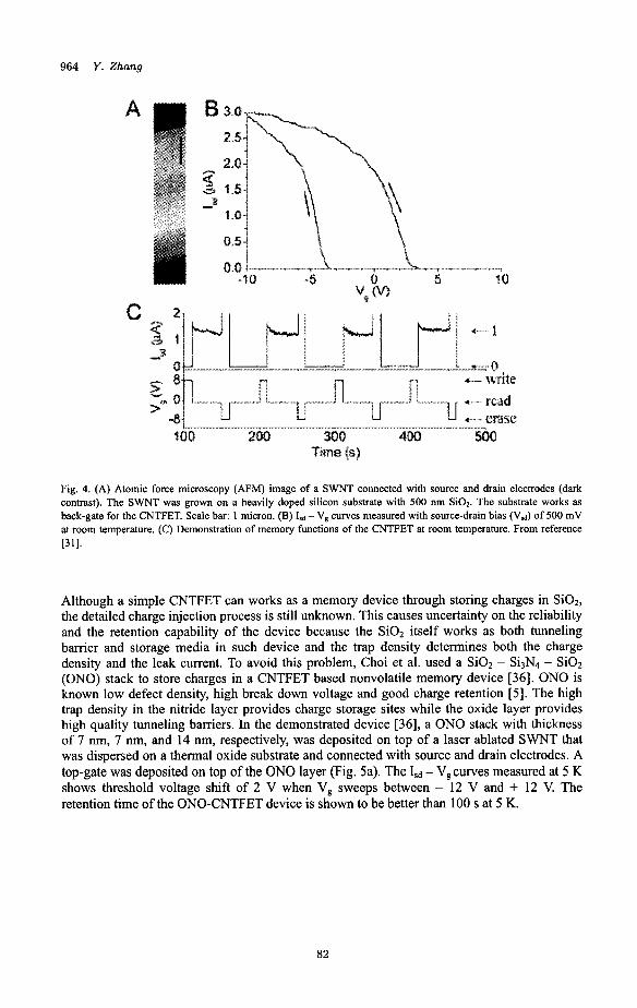
964 Y. Zhang
frme (s)
Fig. 4. (A) Atomic force microscopy (AFM) image of a SWNT connected with source and drain electrodes (dark contrast). The SWNT was grown on a heavily doped silicon substrate with 500 nm SO2. The substrate works as back-gate for the CNTFET. Scale bar: 1 micron. (B) Id - V, curves measured with source-drain bias (VSa) of 500 mV at room temperature. (C) Demonstration of memory functions of the CNTFET at room temperature. From reference ~311.
Although a simple CNTFET can works as a memory device through storing charges in SO2, the detailed charge injection process is still unknown. This causes uncertainty on the reliability and the retention capability of the device because the Si02 itself works as both tunneling barrier and storage media in such device and the trap density determines both the charge density and the leak current. To avoid this problem, Choi et al. used a S O 2 - Si3N4 - Si02 (ONO) stack to store charges in a CNTFET based nonvolatile memory device [36]. ON0 is known low defect density, high break down voltage and good charge retention [5]. The high trap density in the nitride layer provides charge storage sites while the oxide layer provides high quality tunneling barriers. In the demonstrated device [36], a ON0 stack with thickness of 7 nm, 7 nm, and 14 nm, respectively, was deposited on top of a laser ablated SWNT that was dispersed on a thermal oxide substrate and connected with source and drain electrodes. A top-gate was deposited on top of the ON0 layer (Fig. 5a). The Isd - V, curves measured at 5 K shows threshold voltage shift of 2 V when V, sweeps between - 12 V and + 12 V. The retention time of the ONO-CNTFET device is shown to be better than 100 s at 5 K.
82
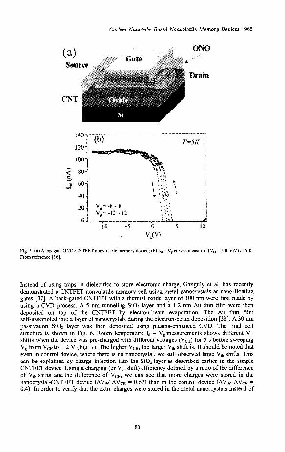
Carbon Nanotube Based Nonvolatile Memory Devices 965
Fig. 5. (a) A top-gate ONO-CNTFET nonvolatile memory device; (b) Isd - V, curves measured (Vsd = 500 mV) at 5 K. From reference [36].
Instead of using traps in dielectrics to store electronic charge, Ganguly et al. has recently demonstrated a CNTFET nonvolatile memory cell using metal nanocrystals as nano-floating gates [37]. A back-gated CNTFET with a thermal oxide layer of 100 nm were first made by using a CVD process. A 5 nm tunneling Si02 layer and a 1.2 nm Au thin film were then deposited on top of the CNTFET by electron-beam evaporation. The Au thin film self-assembled into a layer of nanocrystals during the electron-beam deposition [38]. A 30 nm passivation Si02 layer was then deposited using plasma-enhanced CVD. The final cell structure is shown in Fig. 6. Room temperature Id - V,measurements shows different Vth shifts when the device was pre-charged with different voltages (VcH) for 5 s before sweeping V, from VCH to + 2 V (Fig. 7). The higher VCH, the larger Vth shift is. It should be noted that even in control device, where there is no nanocrystal, we still observed large Vth shifts. This can be explained by charge injection into the Si02 layer as described earlier in the simple CNTFET device. Using a charging (or Vth shift) efficiency defined by a ratio of the difference of Vth shifts and the difference of VCH, we can see that more charges were stored in the nanocrystal-CNTFET device (AVth/ AVCH = 0.67) than in the control device (AVtd AVCH = 0.4). In order to verify that the extra charges were stored in the metal nanocrystals instead of
83
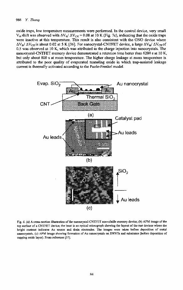
oxide traps, low temperature measurements were performed. In the control device, very small. Vtb shift was observed with AVd AVCH = 0.08 at 10 K (Fig. 7c), indicating that the oxide traps were inactive at this temperature. This result is also consistent with the OW0 device where AV&I A V c ~ is about 0.02 at 5 K [36]. For nanocrystal-CNTFET device, a large AVd AVCH of 0.5 was observed at 10 K, which was attributed to the charge injection into nanocrystals. The ~ ~ o c ~ s t a ~ " ~ T F E T memory device demonstrated a retention time better than 6200 s at I0 K, but only about 800 s at room temperature. The higher charge leakage at room temperature is attributed to the poor quality of evaporated tunneling oxide in which trapassisted leakage current i s thermally activated according to the Poole-Frenkel model.
Evap. SiO u nanocrystal
CNT
Pig. 6. (a) A cross-section illuslxation of the nanocrystal-CNTFET nonvolatile memory device; @) AFM image of the top surface of a CNTFET device; the inset is an optical micrograph showing the layout of the test devices where the bright contrast indicates Au source and drain electrodes. The images were taken before deposition of metal nanocrystals. (c) AFM image showing formation of Au nanocrystals on SWNTs and substrates (before deposition of capping oxide layer). From reference [37].
84
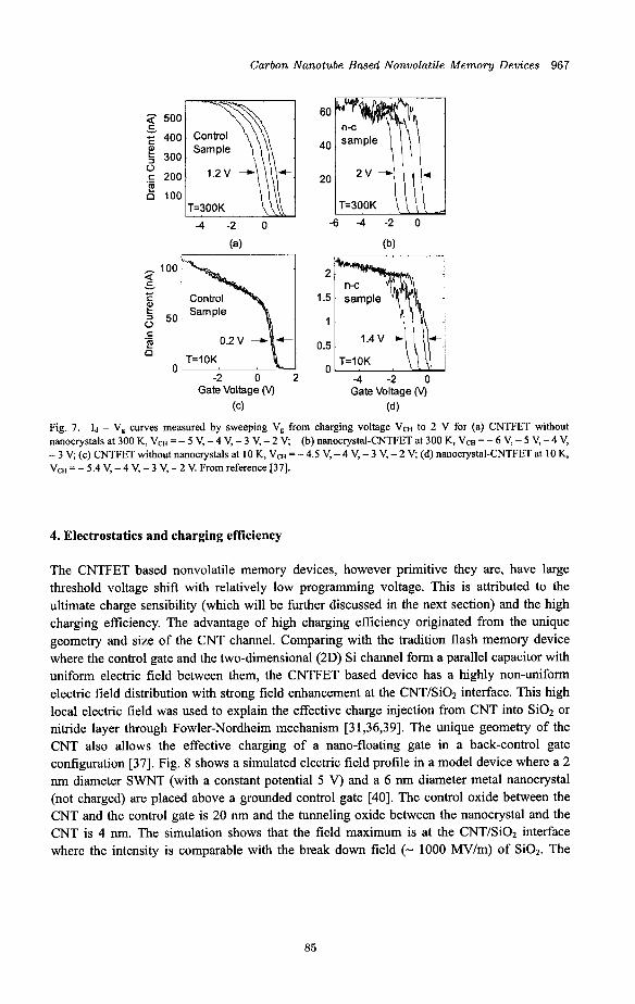
Carbon Nanotube Based Nonvolatile Memory Devices 967
Sample
.- E 100
-4 -2 0 -6 -4 -2 0
-2 0 2 Gate Voltage (v)
(c)
2
1.5
1
0.5
0 -4 -2 0 Gate Voltage (v)
(4 Fig. 7 . Id - V, curves measured by sweeping V, from charging voltage VCH to 2 V for (a) CNTFET without nanocrystals at 300 K, VCH = - 5 V, - 4 V, - 3 V, - 2 V; (b) nanocrystal-CNTFET at 300 K, VCH = - 6 V, - 5 V, - 4 V, - 3 V; (c) CNTFET without nanocrystals at 10 K, V C ~ = - 4.5 V, - 4 V, - 3 V, - 2 V; (d) nanocrystal-CNTFET at 10 K, VCH = - 5.4 V, - 4 V, - 3 V, - 2 V. From reference 1371.
4. Electrostatics and charging efficiency
The CNTFET based nonvolatile memory devices, however primitive they are, have large threshold voltage shift with relatively low programming voltage. This is attributed to the ultimate charge sensibility (which will be further discussed in the next section) and the high charging efficiency. The advantage of high charging efficiency originated from the unique geometry and size of the CNT channel. Comparing with the tradition flash memory device where the control gate and the two-dimensional (2D) Si channel form a parallel capacitor with uniform electric field between them, the CNTFET based device has a highly non-uniform electric field distribution with strong field enhancement at the CNT/Si02 interface. This high local electric field was used to explain the effective charge injection from CNT into Si02 or nitride layer through Fowler-Nordheim mechanism [3 1,36,39]. The unique geometry of the CNT also allows the effective charging of a nano-floating gate in a back-control gate configuration [37]. Fig. 8 shows a simulated electric field profile in a model device where a 2 nm diameter SWNT (with a constant potential 5 V) and a 6 nm diameter metal nanocrystal (not charged) are placed above a grounded control gate [40]. The control oxide between the CNT and the control gate is 20 nm and the tunneling oxide between the nanocrystal and the CNT is 4 nm. The simulation shows that the field maximum is at the CNT/Si02 interface where the intensity is comparable with the break down field (- 1000 MV/m) of Si02. The
85
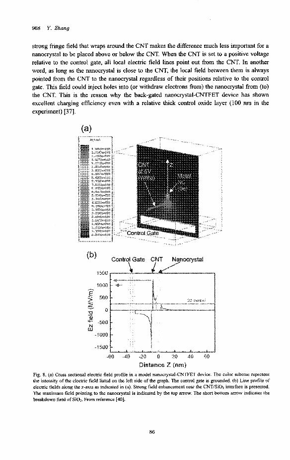
968 Y. Zhang
strong fringe field that wraps around the CNT makes the difference much less important for a nanocrystal to be placed above or below the CNT. When the CNT is set to a positive voltage relative to the control gate, all local electric field lines point out from the CNT. In another word, as long as the nanocrystal is close to the CNT, the local field between them is always pointed from tbe CNT to the nanocrystal regardless of their positions relative to the control gate. This field could inject holes into (or withdraw electrons kom) the nanocrystal from (to) the CNT. This is the reason why the back-gated nanocrystal-CNTFET device has shown excellent charging efficiency even with a relative thick control oxide layer (100 nm in the experiment) [37].
1000 “C
E zj 500
0
-500
-1000
-1500 . . L & U
-60 -40 -20 0 20 40 60
~i~~~~~~ Z fnm) Fig. 8. (a) Cross sectional electric field profile in a model nanocrystal-CNTFET device. The color scheme represent the intensity of the electric field listed on the left side of the graph. The control gate is grounded. (b) Line profile of electric fields along the z-axis as indicated in (a). Strong field enhancement near the CNT/SiOZ interface is presented. The maximum field pointing to the nanocrystal is indicated by the top arrow. The short bottom arrow indicates the breakdown field of SiO2. From reference j401.
86
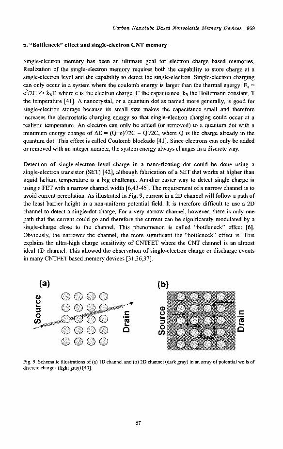
Carbon Nanotube Based Nonvolatile Memory Devices 969
5. “Bottleneck” effect and single-electron CNT memory
Single-electron memory has been an ultimate goal for electron charge based memories. Realization of the single-electron memory requires both the capability to store charge at a single-electron level and the capability to detect the single-electron. Single-electron charging can only occur in a system where the coulomb energy is larger than the thermal energy: E, = e2/2C >> kBT, where e is the electron charge, C the capacitance, kB the Boltzmann constant, T the temperature [41]. A nanocrystal, or a quantum dot as named more generally, is good for single-electron storage because its small size makes the capacitance small and therefore increases the electrostatic charging energy so that single-electron charging could occur at a realistic temperature. An electron can only be added (or removed) to a quantum dot with a minimum energy change of AE = (Q+e)’/2C - Q2/2C, where Q is the charge already in the quantum dot. This effect is called Coulomb blockade [41]. Since electrons can only be added or removed with an integer number, the system energy always changes in a discrete way.
Detection of single-electron level charge in a nano-floating dot could be done using a single-electron transistor (SET) [42], although fabrication of a SET that works at higher than liquid helium temperature is a big challenge. Another easier way to detect single charge is using a FET with a narrow channel width [6,43-451. The requirement of a narrow channel is to avoid current percolation. As illustrated in Fig. 9, current in a 2D channel will follow a path of the least bamer height in a non-uniform potential field. It is therefore difficult to use a 2D channel to detect a single-dot charge. For a very narrow channel, however, there is only one path that the current could go and therefore the current can be significantly modulated by a single-charge close to the channel. This phenomenon is called “bottleneck” effect [6]. Obviously, the narrower the channel, the more significant the “bottleneck” effect is. This explains the ultra-high charge sensitivity of CNTFET where the CNT channel is an almost ideal 1D channel. This allowed the observation of single-electron charge or discharge events in many CNTFET based memory devices [3 1,36,37].
Fig. 9. Schematic illustrations of (a) ID channel and (b) 2D channel (dark gray) in an array of potential wells of discrete charges (light gray) [40].
87
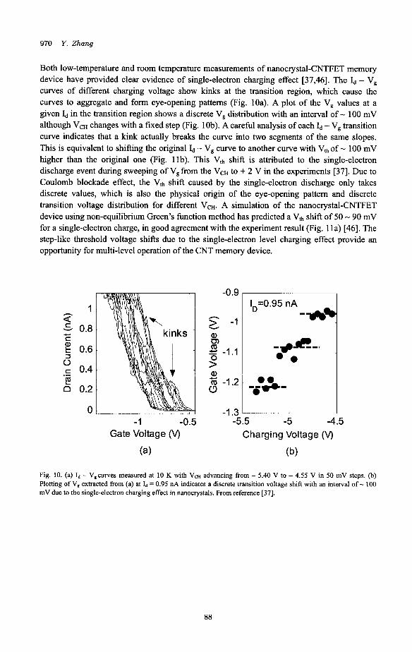
970 Y. Zhang
Both low-temperature and room temperature measurements of nanocrystal-CNTFET memory device have provided clear evidence of single-electron charging effect [37,46]. The I d - V, curves of different charging voltage show kinks at the transition region, which cause the curves to aggregate and form eye-opening patterns (Fig. lOa). A plot of the V, values at a given Id in the transition region shows a discrete V, distribution with an interval of - 100 mV although VCH changes with a fixed step (Fig. lob). A careful analysis of each Id - V, transition curve indicates that a kink actually breaks the curve into two segments of the same slopes. This is equivalent to shifting the original Id - v, curve to another curve with v t h of - 100 mV higher than the original one (Fig. llb). This v t h shift is attributed to the single-electron discharge event during sweeping of V, from the VCH to + 2 V in the experiments [37]. Due to Coulomb blockade effect, the Vth shift caused by the single-electron discharge only takes discrete values, which is also the physical origin of the eye-opening pattern and discrete transition voltage distribution for different VcH. A simulation of the nanocvstal-CNTFET device using non-equilibrium Green’s function method has predicted a Vth shift of 50 - 90 mV for a single-electron charge, in good agreement with the experiment result (Fig. l la) [46]. The step-like threshold voltage shifts due to the single-electron level charging effect provide an opportunity for multi-level operation of the CNT memory device.
1
2 c. 0.8
!! 0.6
h
C
5 n 0.2
c 0.4 e .-
0
-0.9
-1 a, 3 >” = -1.1
a, 4-l a -1.2 c3
-1.3
1,=0.95 nA
-1 -0.5 -5.5 -5 -4.5 Gate Voltage (V) Charging Voltage (V)
(a) (b)
Fig. 10. (a) Id - V,curves measured at 10 K with VCH advancing from - 5.40 V to - 4.55 V in 50 mV steps. (b) Plotting of V, extracted from (a) at Id = 0.95 nA indicates a discrete transition voltage shift with an interval of - 100 mV due to the single-electron charging effect in nanocrystals. From reference [37].
88
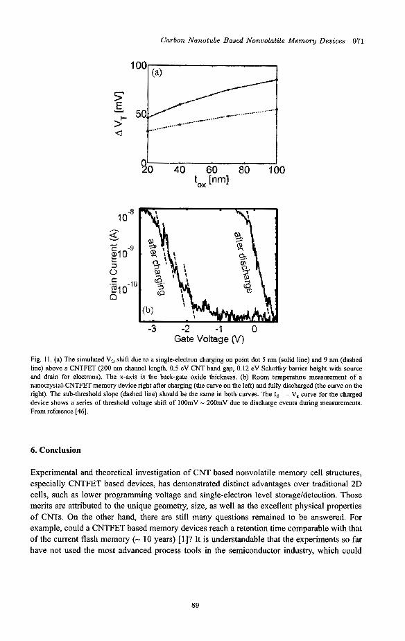
Carbon Nanotube Based Nonvolatile Memory Devices 971
-3 -2 -1 0 Gate Voltage ('4)
Fig. 11. (a) The simulated Vth shift due to a single-electron charging on point dot 5 nm (solid line) and 9 nm (dashed line) above a CNTFET (200 nm channel length, 0.5 eV CNT band gap, 0.12 eV Schottky barrier height with source and drain for electrons). The x-axis is the back-gate oxide thickness. (b) Room temperature measurement of a nanocrystal-CNTFET memory device right after charging (the curve on the left) and fully discharged (the curve on the right). The suh-threshold slope (dashed line) should be the same in both curves. The Id - V, curve for the charged device shows a series of threshold voltage shift of lOOmV - 200mV due to discharge events during measurements. From reference [46].
6. Conclusion
Experimental and theoretical investigation of CNT based nonvolatile memory cell structures, especially CNTFET based devices, has demonstrated distinct advantages over traditional 2D cells, such as lower programming voltage and single-electron level storage/detection. Those merits are attributed to the unique geometry, size, as well as the excellent physical properties of CNTs. On the other hand, there are still many questions remained to be answered. For example, could a CNTFET based memory devices reach a retention time comparable with that of the current flash memory (- 10 years) [l]? It is understandable that the experiments so far have not used the most advanced process tools in the semiconductor industry, which could
89
972 Y. Zhang
result in very low quality of tunneling oxide and cause the deterioration of the retention time [37]. However, a theoretic analysis of such problem is apparently necessary to predict the performance limit of an ideal CNTFET memory device. In addition to the device structure itself, there are many other challenges in the material side that could prevent the application of CNT based memory devices. One major challenge is that CNTs are produced as a mixture of different types, metallic or semiconducting. Most device applications require a single type of nanotubes, for example, pure semiconducting tubes for CNTFETs. Another big challenge is that CNTs as molecular nanomaterials are very hard to be handled using traditional top-down fabrication technology in semiconducting industry. This obstacle also exists for other electronic applications of CNTs, such as CNTFETs in logic circuits. A novel bottom-up approach, such as type-selective self-assembly, is needed for practical high-volume manufacturing of CNT based electronic devices.
Acknowledgements
The author appreciates the contribution from Udayan Ganguly, Edwin Kan and Jing Guo.
References
1. 2.
3.
4.
5.
6.
7.
8.
9.
10.
"International Technology Roadmap for Semiconductors," http://i,ublic.ilrs.net/. S. Tiwari, F. Rana, H. Hanafi, A. Hartstein, E. F. Crabbe, K. Chan, "A silicon nanocrystals based memory," Applied Physics Letters, Vol. 68, pp. 1377-1379, 1996. K. K. Likharev, "Layered tunnel bamers for nonvolatile memory devices," Applied Physics Letters, Vol. 73, pp. 2137-2139, 1998. M. H. White, D. A. Adams, J. K. Bu, "On the go with SONOS," IEEE Circuits & Devices,
H. Bachhofer, H. Reisinger, E. Bertagnolli, H. von Philipsbom, "Transient conduction in multidielectric silicon-oxide-nitride-oxide semiconductor structures," Journal of Applied Physics, Vol. 89, pp. 2791-2800,2001. M. Saitoh, E. Nagata, T. Hiramoto, "Large memory window and long charge-retention time in ultranarrow-channel silicon floating-dot memory," Applied Physics Letters, Vol.
P. Xuan, M. She, B. Harteneck, A. Liddle, J. Bokor, T.-J. King, "FinFET SONOS flash memory for embedded applications," IEDM '03 Technical Digest, pp. 26.4.1 - 26.4.4, 2003. M. S. Dresselhaus, G. Dresselhaus, P. C. Eklund. Science of Fullerenes and Carbon Nanotubes (Academic, San Diego, 1996). M. S. Dresselhaus, G. Dresselhaus, P. Avouris (eds.) Carbon Nanotubes: Synthesis, Structure, Properties, and Applications (Springer, Berlin, 200 1). Y. K. Kwon, D. Tomanek, S. Iijima, ""Bucky shuttle" memory device: Synthetic approach and molecular dynamics simulations," Physical Review Letters, Vol. 82, pp. 1470- 1473, 1999.
Vol. 16, pp. 22-31, 2000.
82, pp. 1787-1789,2003.
90
Carbon Nanotube Based Nonvolatile Memory Devices 973
11. B. W. Smith, M. Monthioux, D. E. Luzzi, "Encapsulated C-60 in carbon nanotubes,"
12. J. W. Kang, H. J. Hwang, "Carbon nanotube shuttle memory device based on Nature, Vol. 396, pp. 323-324, 1998.
singlewall-to-doublewall carbon nanotube transition," Computational Materials Science, VOI. 33, pp. 338-345,2005.
13. J. W. Kang, H. J. Hwang, "'Carbon nanotube shuttle' memory device," Carbon, Vol. 42, pp.
14. D. Ostling, D. Tomanek, A. Rosen, "Electronic structure of single-wall, multiwall, and
15. J. Lee, H. Kim, S. J. Kahng, G. Kim, Y W. Son, J. Ihm, H. Kato, Z. W. Wang, T. Okazaki,
3018-3021,2004.
filled carbon nanotubes," Physical Review B, Vol. 55, pp. 13980-13988, 1997.
H. Shinohara, Y. Kuk, "Bandgap modulation of carbon nanotubes by encapsulated metallofullerenes," Nature, Vol. 41 5 , pp. 1005-8,2002.
16. D. E. Luzzi, B. W. Smith, "Carbon cage structures in single wall carbon nanotubes: a new class of materials," Carbon, Vol. 38, pp. 1751-1756,2000.
17. S. Bandow, M. Takizawa, K. Hirahara, M. Yudasaka, S. Iijima, "Raman scattering study of double-wall carbon nanotubes derived from the chains of fullerenes in single-wall carbon nanotubes," Chemical Physics Letters, Vol. 337, pp. 48-54,2001.
18. T. Rueckes, K. Kim, E. Joselevich, G. Y. Tseng, C. L. Cheung, C. M. Lieber, "Carbon nanotube-based nonvolatile random access memory for molecular computing," Science, VOI. 289, pp. 94-7, 2000.
19. J. C. Scott, "Is there an immortal memory?," Science, Vol. 304, pp. 62-63,2004. 20. J. W. Ward, M. Meinhold, B. M. Segal, J. Berg, R. Sen, R. Sivarajan, D. K. Brock, T.
Rueckes, "A nonvolatile nanoelectromechanical memory element utilizing a fabric of carbon nanotubes," Proceedings of 2004 Non-Volatile Memory Technology Symposium, pp. 34 - 38,2004.
21. J. W. Kang, J. H. Lee, H. J. Lee, H. J. Hwang, "A study on carbon nanotube bridge as a electromechanical memory device," Physica E-Low-Dimensional Systems & Nanostructures, Vol. 27, pp. 332-340,2005.
single carbon nanotube," Nature, Vol. 393, pp. 49-52, 1998.
field-effect transistors," Nature, Vol. 424, pp. 654-657,2003.
22. S. J. Tans, A. R. M. Verschueren, C. Dekker, "Room-temperature transistor based on a
23. A. Javey, J. Guo, Q. Wang, M. Lundstrom, H. J. Dai, "Ballistic carbon nanotube
24. P. Avouris, "Molecular electronics with carbon nanotubes," Acc Chem Res, Vol. 35, pp.
25. P. McEuen, M. S. Fuhrer, H. Park, "Single-walled carbon nanotub electronics," IEEE Transaction on Nanotechnology, Vol. 1, pp. 78 - 85,2002.
26. J. Kong, N. R. Franklin, C. W. Zhou, M. G. Chapline, S. Peng, K. J. Cho, H. J. Dai, "Nanotube molecular wires as chemical sensors," Science, Vol. 287, pp. 622-625,2000.
27. A. Star, T. R. Han, V. Joshi, J. C. P. Gabriel, G. Gruner, "Nanoelectronic carbon dioxide sensors," Advanced Materials, Vol. 16, pp. 2049-+, 2004.
28. K. Bradley, J. Cumings, A. Star, J. C. P. Gabriel, G. Gruner, "Influence of mobile ions on nanotube based FET devices," Nan0 Letters, Vol. 3, pp. 639-641,2003.
1026-34,2002.
91
974 Y. Zhang
29. R. J. Chen, Y. Zhang, D. Wang, H. Dai, "Noncovalent sidewall functionalization of single-walled carbon nanotubes for protein immobilization," Journal of American Chemical Society, Vol. 123, pp. 3838-9,2001.
30. R. J. Chen, S. Bangsaruntip, K. A. Drouvalakis, N. W. Kam, M. Shim, Y. Li, W. Kim, P. J. Utz, H. Dai, "Noncovalent functionalization of carbon nanotubes for highly specific electronic biosensors," Proceedings of the National Academy of Sciences, Vol. 100, pp.
31. M. S. Fuhrer, B. M. Kim, T. Durkop, T. Brintlinger, "High-mobility nanotube transistor
32. M. Radosavljevic, M. Freitag, K. V. Thadani, A. T. Johnson, "Nonvolatile molecular
4984-9,2003.
memory," Nan0 Letters, Vol. 2, pp. 755-759,2002.
memory elements based on ambipolar nanotube field effect transistors," Nan0 Letters, Vol. 2, pp. 761-764,2002.
33. J. B. Cui, R. Sordan, M. Burghard, K. Kern, "Carbon nanotube memory devices of high
34. W. Kim, A. Javey, 0. Vermesh, 0. Wang, Y. M. Li, H. J. Dai, "Hysteresis caused by water charge storage stability," Applied Physics Letters, Vol. 81, pp. 3260-3262,2002.
molecules in carbon nanotube field-effect transistors," Nan0 Letters, Vol. 3, pp. 193-198, 2003.
nanotube-based field effect transistors," Diamond and Related Materials, Vol. 13, pp. 35. D. J. Yang, Q . Zhang, S. G Wang, G. F. Zhong, "Memory effects of carbon
1967-1970,2004. 36. W. B. Choi, S. Chae, E. Bae, J. W. Lee, B. H. Cheong, J. R. Kim, J. J. Kim,
"Carbon-nanotube-based nonvolatile memory with oxide-nitride-oxide film and nanoscale channel," Applied Physics Letters, Vol. 82, pp. 215-277,2003.
37. U. Ganguly, E. C. Kan, Y. Zhang, "Carbon nanotube-based nonvolatile memory with charge storage in metal nanocrystals," Applied Physics Letters, Vol. 87, pp. 043108,2005.
38. Z. T. Liu, C. Lee, V. Narayanan, G. Pei, E. C. Kan, "Metal nanocrystal memories - Part I: Device design and fabrication," IEEE Transactions on Electron Devices, Vol. 49, pp. 1606- 1613,2002.
39. A. Robert-Peillard, S. V. Rotkin, "Modeling hysteresis phenomena in nanotube
40. Y. Zhang, E. C. Kan, U. Ganguly, J. Guo. in Materials Research Society 2005 Spring
41. H. Grabert, M. H. Devoret (eds.) SingIe charge tunneling : Coulomb blockade phenomena
42. C. D. Chen, Y. Nakamura, J. S. Tsai, "Aluminum single-electron nonvolatile floating gate
43. K. Yano, T. Ishii, T. Hashimoto, T. Kobayashi, F. Murai, K. Seki, "Room-Temperature
field-effect transistors," Ieee Transactions on Nanotechnology, Vol. 4, pp. 284-288,2005.
Meeting (San Francisco, CA, 2005).
in nanostructures (Plenum Press, New York, 1992).
memory cell," Applied Physics Letters, Vol. 71, pp. 2038-2040, 1997.
Single-Electron Memory," IEEE Transactions on Electron Devices, Vol. 41, pp.
44. L. J. Guo, E. Leobandung, S. Y. Chou, "A room-temperature silicon single-electron 1628-1638, 1994.
metal-oxide-semiconductor memory with nanoscale floating-gate and ultranarrow channel," Applied Physics Letters, Vol. 70, pp. 850-852, 1997.
92
Carbon Nanotube Based Nonvolatile Memory Devices 975
45. G. Molas, B. De Salvo, G. Ghibaudo, D. Mariolle, A. Toffoli, N. Buffet, R. Puglisi, S. Lombardo, S. Deleonibus, "Single electron effects and structural effects in ultrascaled silicon nanocrystal floating-gate memories," IEEE Transactions on Nanotechnology, Vol. 3, pp. 42-48,2004.
46. J. Guo, E. C . Kan, U. Ganguly, Y. Zhang. (to be published).
93

This page intentionally left blankThis page intentionally left blank
World Scientific www.worldscimtific.com
Internat ional Journal of High Speed Electronics a n d Systems
@ World Scientific Publ ishing Company Vol. 16, NO. 4 (2006) 977-999
SINGLE-WALLED CARBON NANOTUBES: APPLICATIONS IN HIGH FREQUENCY ELECTRONICS
P.J. BURKE, C. RUTHERGLEN, Z. YU
Integrated Nanosystems Research Facility Department of Electrical Engineering and Computer Science
University of California, Irvine Irvine, California 92697-2625
In this paper, we review the potential applications of single-walled carbon nanotubes in three areas: passives (interconnects), actives (transistors), and antennas. In the area of actives, potential applications include transistors for RF and microwave amplifiers, mixers, detectors, and filters. We review the experimental state of the art, and present the theoretical predictions (where available) for ultimate device performance. In addition, we discuss fundamental parameters such as dc resistance as a function of length for individual, single-walled carbon nanotubes.
Keywords: Nanotube; interconnect; amplifier; antenna.
1. Introduction
The development of carbon nanotube synthesis, both for single-walled nanotubes (SWNTs) and multi-walled nanotubes (MWNTs), and of nanotube device physics has been rapid in the previous decade. The sphere of potential applications is broad due to their superior mechanical, thermal, and electrical properties. These have been reviewed in several recent monographs[l-71, as well as other manuscripts in this volume. However, an intriguing sphere of application which has until recently received relatively minor attention is in the area of high speed (RF, microwave, mm-wave, and THz) electronics. At first glance, the idea of combining nanotechnology with RF circuitry may seem to be a rather poor match, due to the typically high impedance of nano-electronics devices. However, the intrinsic speed limit of carbon nanotube devices can be very high, up to the THz range, so that on hrther reflection it seems potentially feasible to fabricate high speed devices and ultimately systems out of carbon nanotubes. The topic of this paper is to discuss how far along we are on the road to this goal, and in what manner it makes sense to even continue development of the technology, at least for high speed systems. Since the progress in synthesis has been very rapid, it is our point of view (at least for this review) that one should evaluate the ultimate potential of the technology, assuming the problems of economical fabrication could be solved.
95
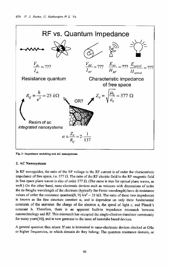
978 P. J . Burke, C. Rutherglen B Z. Yu
RF vs. Quantum Impedance
Resistance quantum Characteristic impedance of free space
h e
R =-- e - -25kR
Realm of ac integrated nanosystems
Fig. 1: Impedance matching and AC nanosystems.
2. AC Nanosystems
In RF waveguides, the ratio of the RF voltage to the RF current is of order the characteristic impedance of free space, i.e. 377 SZ. The ratio of the RF electric field to the RF magnetic field in free space plane waves is also of order 377 R. (The same is true for optical plane waves, as well.) On the other hand, nano-electronic devices such as resistors with dimensions of order the de Broglie wavelength of the electrons (typically the Fermi wavelength) have dc resistance values of order the resistance quantum[8, 91 We2 = 25 kQ. The ratio of these two impedances is known as the fine structure constant a, and is dependent on only three fundamental constants of the universe: the charge of the electron e, the speed of light c, and Planck’s constant h. Therefore, there is an apparent built-in impedance mismatch between nanotechnology and RF. This mismatch has occupied the single-electron-transistor community for many years[ 101, and is now germane to the issue of nanotube based devices.
A general question thus arises: If one is interested in nano-electronic devices clocked at GHz or higher frequencies, to which domain do they belong: The quantum resistance domain, or
96
Single- Walled Carbon Nanotubes 979
the free space impedance domain? It appears that there is no general answer to this question. However, we can make the following general claims: First, if an individual nano-device is to talk to the outside world, it will need to drive an impedance of order the characteristic impedance of free space. In this case, the impedance matching problem must be dealt with and cannot be ignored.
However, a paradigm we have recently advocated[ 111 is one of integrated nanosystems, in which nanotubes and nanowires are used both as the active elements and as the interconnects. In this case, the devices can all be dealt with in the realm of the resistance quantum, and still operate at ultra-high speeds. Such a paradigm is worth further investigating, but our conclusions will become clearer on this issue below.
3. SWNT electronic properties
The electronic properties of SWNTs vary, depending on their diameter and chirality[l2]. The chirality determines whether the nanotube behaves as a metal or semiconductor. Experimentally, metallic nanotubes are typically distinguished by the absence of a dependence of the small bias conductance on a gate voltage. Similarly, semiconducting nanotubes have a conductance that depends strongly on the gate voltage. The band-gap of semiconducting nanotubes is related to the diameter through the E, = 0.9 eV/d[nm], where d is the diameter in nm.
4. Synthesis
Since the original development of chemical vapor deposition (CVD) for nanotube synthesis from lithographically defined catalyst pads was developed in 1998[13], many groups around the world have continued to focus on using CVD for synthesis. In this section, we focus on a particular metric, that is the synthesis of relatively long single-walled carbon nanotubes. The reason, as will become clear below, is that nanotubes may have a role to play as interconnects and the synthesis of long tubes is a necessary step in that direction. Additionally, long SWNTs allow one to measure the resistivity without wony about contact resistance effects. In Fig. 2, we show an SEM image (from ref. [14], with permission) of an electrically contacted, 0.4 cm long SWNT synthesized in our labs.
97
980 P. 9. Burke, C. Rutherglen €4 2. Yu
Fig. 2: Electrically contacted, 0.4 em long SWNT, from 1151.
In Fig. 3, we show a plot o f length vs. year o f electrically contacted, individual S W T s (adapted from 1151, with permission). (Data for figs. 3,4 from references 114, 16-37].) The progress has indeed been rapid. In addition, the tubes grown in CVD are h i ~ l i ~ t e $ in red, ind~cating that the growth technique has had a significant impact on the synthesis of long nanotubes. In Fig. 4, we show the length vs. year of all individual S W T s . The electrically contacted S W T s are circled in red. The progress has been about an order o f magnitude increase in length per year. Such progress is rapid, even by the modern standards of electronics technoliogy. It remains to be seen if and when such progress will plateau.
98
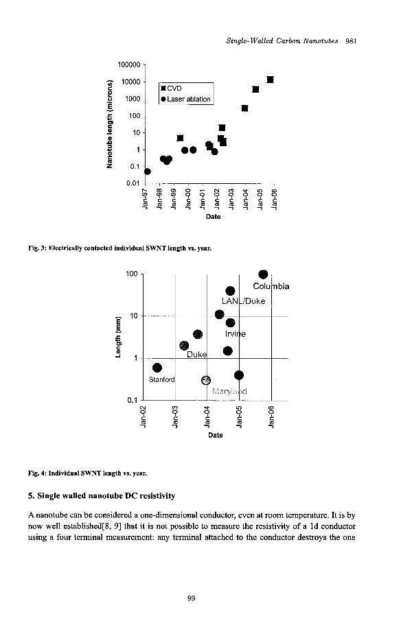
Single- Walled Carbon Nanotubes 981
- c, 100 -
I
Fig. 3: Electrically contacted individual SWNT length vs. year.
100
- 10 E E 5
d 1
- 0) C a3
0.1 1 CV m d In (D
m 7
C m 7
9 m 7
4 C 9 4 m 7
C m 7
4
Date
Fig. 4: Individual SWNT length vs. year.
5. Single walled nanotube DC resistivity
A nanotube can be considered a one-dimensional conductor, even at room temperature. It is by now well established[8, 91 that it is not possible to measure the resistivity of a Id conductor using a four terminal measurement: any terminal attached to the conductor destroys the one
99
982 P. J . Burke, C. Rutherglen & Z. Yu
dimensional nature of the conduction. Therefore, one can only perform a two-terminal measurement, and the contact resistance must be addressed.
For Id systems that are in the ballistic limit (i.e. length less than the mean free path), the contact resistance is always greater than or equal to We2 = 25 162. In SWNTs, this number is modified by a factor of 2 for band structure degeneracy and a factor of 2 for spin[l2], so that the lowest possible resistance a SWNT can have (when it is shorter than the m.f.p.) is W4e2 =
6 162. However, in cases where the contact is poor (for example, if there is a Schottky bamer at the metalhanotube interface), the resistance can be and typically is much higher. Recent work has shown that use of Pd as the contact material allows the theoretical limit to be reached, at least for very short SWNTs[38-40]. Prior to this, the more commonly used metal was Au and gave resistances of order MR, which was due to the poor contact.
On the other hand, if the nanotube is long compared to the mean-free path, then the resistance will have a component that scales linearly with length. Exactly how long is the mean free path in a SWNT? This question has not been definitively answered, but by plotting the resistance vs. length for tubes of a variety of different lengths, one can get a reasonable estimate. To date, no studies have been published investigating this in full detail, so we are forced to use results from the literature, which will be expected to have a variation due to different processing conditions, different nanotube diameters, different measurement temperatures, and different species (i.e. metallic or semiconducting). Although the amount of data on nanotubes in the limit that the contact resistance is small is not large (there are only a few publications), the curve plotted in Fig. 5 (adopted from ref. [14], using data from refs. [14, 35, 38, 40-431) shows a remarkably consistent trend: nanotubes with length less than about 1 micron can approach the ballistic limit. On the other hand, nanotubes with length greater than about 1 micron have a resistance per unit length of about 6 W p m . This indicates a mean-free path of about 1 pm, since (neglecting the contact resistance) the equation for the m.f.p. in Id diffusive conductors is[8]:
Remarkably, this indicates as 3d resistivity (assuming a diameter of 1.5 nm) of 1.1 @-cm, which is lower than bulk copper (which has a value of 1.7 pR-cm). Thus, if a tightly packed array of SWNTs could be synthesized economically, the material would be a potentially disruptive technology for interconnects in integrated circuits. This motivates our discussion of the high frequency properties of single walled nanotubes as conductors.
100
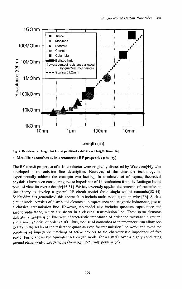
Single- Walled Carbon Nanotubes 983
1GOhm I I I I
100MOhm
W Columbia
1 OMOhm -Ballistic limit t - - - Scaling 6 k R / p
(lowest contact resistance allowed by quantum mechanics)
v n.
.- 0
0
1 Onm 1 OOpm 1 Omm
Length (m) Fig. 5: Resistance vs. length for lowest published value at each length, from [141.
6. Metallic nanotubes as interconnects: RF properties (theory)
The RF circuit properties of a Id conductor were originally discussed by Wesstrom[44], who developed a transmission line description. However, at the time the technology to experimentally address the concepts was lacking. In a related set of papers, theoretical physicists have been considering the ac impedance of 1 d conductors from the Luttinger liquid point of view for over a decadet45-511. We have recently applied the concepts of transmission line theory to develop a general RF circuit model for a single walled nanotubeC52-551. Salahuddin has generalized this approach to include multi-mode quantum wires[56]. Such a circuit model consists of distributed electrostatic capacitance and magnetic inductance, just as a classical transmission line. However, the model also includes quantum capacitance and kinetic inductance, which are absent in a classical transmission line. These extra elements describe a transmission line with characteristic impedance of order the resistance quantum, and a wave velocity of order c/100. Thus, the use of nanotubes as interconnects can allow one to stay in the realm of the resistance quantum even for transmission line work, and avoid the problems of impedance matching of active devices to the characteristic impedance of free space. Fig. 6 shows the equivalent RF circuit model for a SWNT over a highly conducting ground plane, neglecting damping (from Ref. [52], with permission).
101
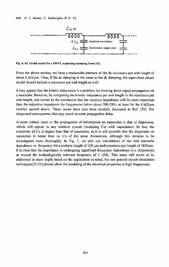
984 P. J . Burke, C. Rutherglen t3 Z. Yu
c,, 1 Electrostatic copnci~nocc I l- I
Fig. 6: RF circuit model for a SWNT, neglecting damping, from [52].
From the above section, we have a reasonable estimate of the dc resistance per unit length of about 6 W p m . Thus, if the ac damping is the same as the dc damping, the equivalent circuit model should include a resistance per unit length as well.
It may appear that the kinetic inductance is a problem for slowing down signal propagation on a nanotube. However, by comparing the kinetic inductance per unit length to the resistance per unit length, one comes to the conclusion that the resistive impedance will be more important than the inductive impedance for frequencies below about 200 GHz, at least for the 6 m / p m number quoted above. These issues have also been recently discussed in Ref. [56]. For integrated nanosystems, this may result in some propagation delay.
A more critical issue to the propagation of information on nanotubes it that of dispersion, which will appear in any resistive system (including Cu) with capacitance. In fact, the resistivity of Cu is higher than that of nanotubes, so it is still possible that the dispersion on nanotubes is better than on Cu of the same dimensions, although this remains to be investigated more thoroughly. In Fig. 7, we plot our calculations of the real nanotube impedance vs. frequency for a realistic length of 100 pm and resistance per length of lm/prn . It is clear that the impedance is undergoing significant frequency dependence (i.e. dispersion) at around the technologically relevant frequency of 1 GHz. This issue still needs to be addressed in more depth based on the application in mind, but our general circuit simulation techniques[ 52-55] should allow for modeling of the electrical properties at high frequencies.
102
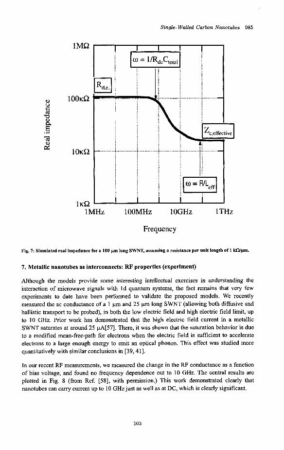
Single- Walled Carbon Nanotubes 985
1MQ
Q) loOK52
4 E .-
! !
1 MHz 1OOMHz
- i
lOGHz lTHz
Frequency
Fig. 7: Simulated real impedance for a 100 pm long SWNT, assuming a resistance per unit length of 1 W p m .
7. Metallic nanotubes as interconnects: RF properties (experiment)
Although the models provide some interesting intellectual exercises in understanding the interaction of microwave signals with Id quantum systems, the fact remains that very few experiments to date have been performed to validate the proposed models. We recently measured the ac conductance of a 1 pm and 25 pm long SWNT (allowing both diffusive and ballistic transport to be probed), in both the low electric field and high electric field limit, up to 10 GHz. Prior work has demonstrated that the high electric field current in a metallic SWNT saturates at around 25 pA[57]. There, it was shown that the saturation behavior is due to a modified mean-free-path for electrons when the electric field is sufficient to accelerate electrons to a large enough energy to emit an optical phonon. This effect was studied more quantitatively with similar conclusions in [39,41].
In our recent RF measurements, we measured the change in the RF conductance as a function of bias voltage, and found no frequency dependence out to 10 GHz. The central results are plotted in Fig. 8 (from Ref. [58], with permission.) This work demonstrated clearly that nanotubes can carry current up to 10 GHz just as well as at DC, which is clearly significant.
103
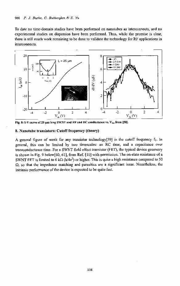
986 P. J . Burke, C. Rutherglen & 2. Yu
To date no time-domain studies have been performed on nanotubes as interconnects, and no experimental studies on dispersion have been performed. Thus, while the promise is clear, there is still much work remaining to be done to validate the technology for RF applications in interconnects.
20 I
Vds (V) s o
-20 -4 -2 0 2 4
VA. (V) I" ""
Fig. 8: I-V curve of 25 pm long SWNT and RF and DC conductance vs. Vd,, from [SS].
8. Nanotube transistors: Cutoff frequency (theory)
A general figure of merit for any transistor technology[59] is the cutoff fiequency fT. In general, this can be limited by two timescales: an RC time, and a capacitance over transconductance time. For a SWNT field effect transistor (FET), the typical device geometry is shown in Fig. 9 below[60, 611, from Ref, [ 113 with permission. The on-state resistance of a SWNT FET is limited to 6 WZ (h/4e2) or higher. This is quite a high resistance compared to 50 R, so that the impedance matching and parasitics are a significant issue. Nonetheless, the intrinsic performance of the device is expected to be quite fast.
104
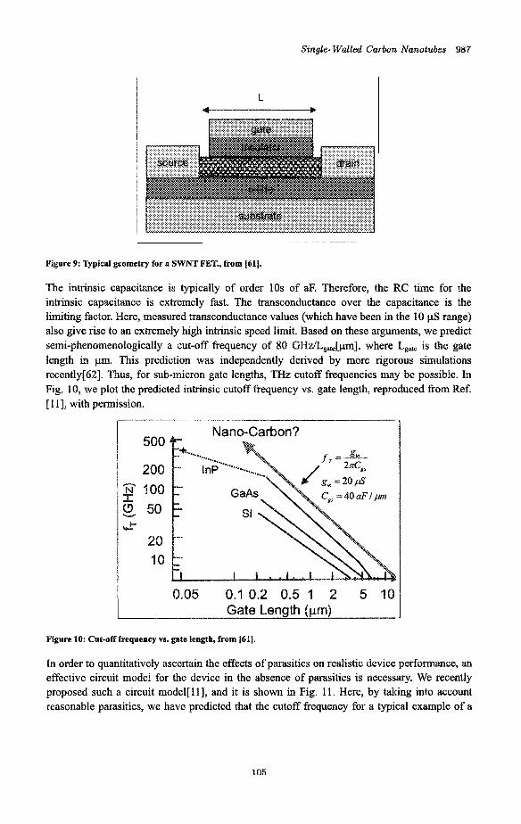
Single- Walled Carbon Nanotubes 987
L
I
Figure 9: Typical geometry for a SWNT FET., from [611.
The intrinsic capacitance is typically of order 10s of aF. Therefore, the RC time for the intrinsic capacitance is extremely fast. The transconductance over the capacitance is the limiting factor. Here, measured transconductance values (which have been in the 10 pS range) also give rise to an extremely high intrinsic speed limit. Based on these arguments, we predict semi-phenomenolo~ical~y a cut-off frequency of 80 CHz/L,,[pmj, where L,, is the gate length in pm. This prediction was independently derived by more rigorous simulations recently[(i%J. Thus, for sub-micron gate lengths, THz cutoff frequencies may be possible. In Fig. 10, we plot the predicted intrinsic cutoff frequency vs. gate length, reproduced from Ref. [ 111, with permission.
500
200 100 50
20 1 Q
0.05 0.1 0.2 0.5 1 2 5 10
Figure 10: Cut-off frequency vs. gate length, from 1611.
In order to quantitatively ascertain the effects of parasitics on realistic device performance, an effective circuit model for the device in the absence of parasitics is necessary. We recently proposed such a circuit model[ll], and it is shown in Fig. 11. Here, by taking into account reasonable parasitics, we have predicted that the cutoff frequency for a typical example of a
105
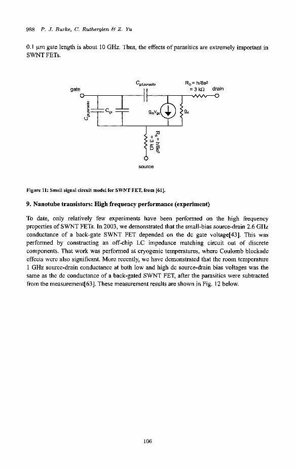
988 P. J . Burke, C. Rutherglen d 2. Yu
0.1 pm gate length is about 10 GHz. Thus, the effects of parasitics are extremely important in SWNT FETs.
gate cgd,parasi6c R, = hBe2
! i = 3 k n drain 1” .......... O-1 e ..... i
J ....., :,: c,, 0 - 1 T
6 source
Figure 11: Small signal circuit model for SWNT FET, from [all.
9. Nanotube transistors: High frequency performance (experiment)
To date, only relatively few experiments have been performed on the high frequency properties of SWNT FETs. In 2003, we demonstrated that the small-bias source-drain 2.6 GHz conductance of a back-gate SWNT FET depended on the dc gate voltage[43]. This was performed by constructing an off-chip LC impedance matching circuit out of discrete components. That work was performed at cryogenic temperatures, where Coulomb blockade effects were also significant. More recently, we have demonstrated that the room temperature 1 GHz source-drain conductance at both low and high dc source-drain bias voltages was the same as the dc conductance of a back-gated SWNT FET, after the parasitics were subtracted from the measurement[63]. These measurement results are shown in Fig. 12 below.
106
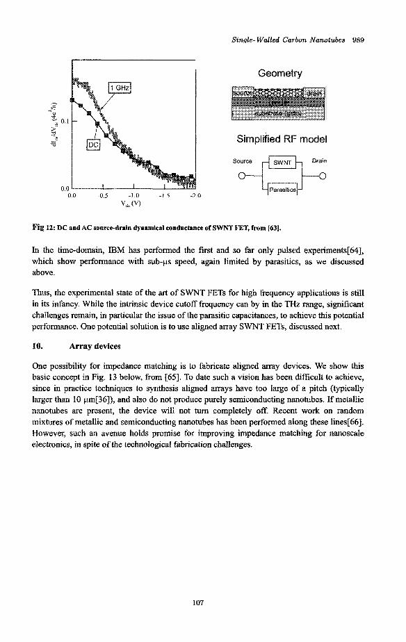
Single- Walled Carbon Nanolubes 989
0.0 -0.5 -1.0 -1.5 -2.0 "d, (v
mg 12: BC and AC so i l~~e-drai~ dynamical conductance of SWNT FET, fmm 1631.
In the time-domain, IBh4 has performed the first and so far only pulsed experiments[&%], which show performance with sub-ys speed, again limited by parasitics, as we discussed above.
Thus, the experimental state of the art of S W T FETs for high frequency applications is still in its infancy. While the intrinsic device cutoff frequency can by in the THz range, significant challenges remain, in particular the issue of the parasitic capacitances, to achieve this p o ~ ~ ~ i a ~ performance. One potential solution is to use aligned array S W T FETs, discussed next.
110. Array devises
One possibility for impedance matching is to fabricate aligned array devices. We show this basic concept in Fig. 13 below, from [65]. To date such a vision has been difficult to achieve, since in practice techniques to synthesis aligned arrays have too large of a pitch (typically larger than 10 ym[36]), and also do not produce purely semiconducting nanotubes. If metallic nanotubes are present, the device will not turn completely off. Recent work on random mixtures of metallic and semiconducting nanotubes has been pedormed along these lines[66]. However, such an avenue holds promise for improving impedance matching for nanoscale electronics, in spite of the ~ e c h n o l o ~ c a ~ fabrication challenges.
107
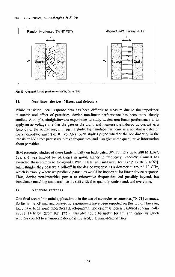
990 P. J . Burke, C. Rutherglen €4 2. Yu
w
1 Randomly oriented SWNT FETs Aligned SWNT array FETs
W
L - L *
1
Fig 13: Concept for aligned array FETs, from [65].
11. Non-linear devices: Mixers and detectors
While transistor linear response data has been difficult to measure due to the impedance mismatch and effect of parasitics, device non-linear performance has been more clearly studied. A simple, straightforward experiment to study device non-linear performance is to apply an ac voltage to either the gate or the drain, and measure the induced dc current as a function of the ac frequency. In such a study, the nanotube performs as a non-linear detector (or a homodyne mixer) of RF voltages. Such studies probe whether the non-linearity in the transistor I-V curve persist up to high frequencies, and also give some quantitative information about parasitics.
IBM presented studies of these kinds initially on back-gated SWNT FETs up to 580 MHz[67, 681, and was limited by parasitics in going higher in frequency. Recently, Cornell has extended these studies to top-gated SWNT FETs, and measured results up to 50 GHz[69]. Interestingly, they observe a roll-off in the device response as a detector at around 10 GHz, which is exactly where we predicted parasitics would be important for linear device response. Thus, device non-linearities persist to microwave frequencies and possibly beyond, but impedance matching and parasitics are still critical to quantify, understand, and overcome.
12. Nanotube antennas
One final area of potential application is in the use of nanotubes as antennas[70, 711 antennas. So far in the RF and microwave, no experiments have been reported on this topic. However, there have been some theoretical developments. The essential idea is captured schematically in Fig. 14 below (from Ref. [72]). This idea could be usehl for any application in which wireless contact to a nanoscale device is required, e.g. nano-scale sensors.
108
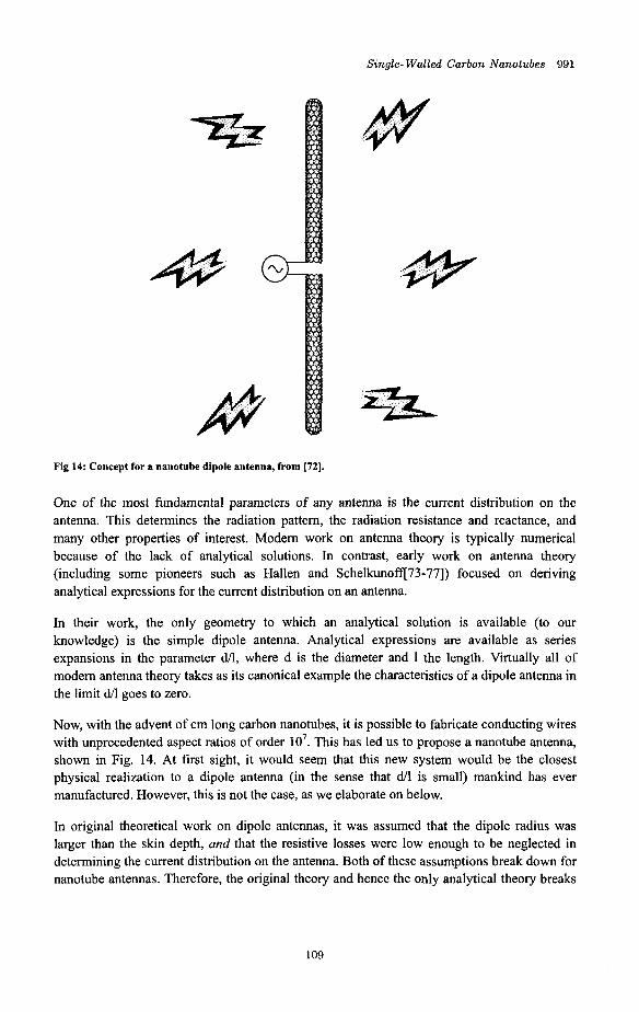
Single- Walled Carbon Nanotubes 991
Fig 14: Concept for a nanotube dipole antenna, from [72].
One of the most fundamental parameters of any antenna is the current distribution on the antenna. This determines the radiation pattern, the radiation resistance and reactance, and many other properties of interest. Modem work on antenna theory is typically numerical because of the lack of analytical solutions. In contrast, early work on antenna theory (including some pioneers such as Hallen and Schelkunoff173-771) focused on deriving analytical expressions for the current distribution on an antenna.
In their work, the only geometry to which an analytical solution is available (to our knowledge) is the simple dipole antenna. Analytical expressions are available as series expansions in the parameter d/l, where d is the diameter and 1 the length. Virtually all of modem antenna theory takes as its canonical example the characteristics of a dipole antenna in the limit d/l goes to zero.
Now, with the advent of cm long carbon nanotubes, it is possible to fabricate conducting wires with unprecedented aspect ratios of order lo7. This has led us to propose a nanotube antenna, shown in Fig. 14. At first sight, it would seem that this new system would be the closest physical realization to a dipole antenna (in the sense that d/l is small) mankind has ever manufactured. However, this is not the case, as we elaborate on below.
In original theoretical work on dipole antennas, it was assumed that the dipole radius was larger than the skin depth, and that the resistive losses were low enough to be neglected in determining the current distribution on the antenna. Both of these assumptions break down for nanotube antennas. Therefore, the original theory and hence the only analytical theory breaks
109
992 P. J . Burke, C. Rutherglen €4 Z. Yu
down in the limit d/l becomes sufficiently small.
In a one-dimensional conductor such as a nanotube, the concept of skin-depth is almost meaningless, since the electrons are only free to move along the length of the wire, and not in the transverse direction. Therefore the current distribution is effectively one-dimensional. In addition to the electron transport occumng in only one dimension, we also have two more important effects: large resistance, and large inductance.
These effects give rise to very different behavior for a nanotube antenna, as compared to a classical antenna. The main difference is the current distribution is periodic with a wavelength about 100 times smaller than the free space wavelength for a given temporal frequency. The comparison of the current distribution on a nanotube dipole antenna to a classical dipole antenna is shown in Fig. 15 below (from Ref.[7O], with permission). It is clear that the current distributions are dramatically different. Our work has been further developed numerically by Hanson[7 13.
NT antenna Wire antenna
Fig 15: Current distribution on a nanotube antenna vs. classical wire antenna. 1 is the free space wavelength
(set by the frequency), and hp is the wavelength of the current distribution on a nanotube, which is typically
about 100 times smaller than the free space wavelength, from [70].
Our calculations[70] show that the efficiency of a classical nanotube dipole antenna is poor, due to resistive losses. However, we have proposed that possibly other geometries (to be
110
Single- Walled Carbon Nanotubes 993
determined) could and should be investigated that take advantage of the unique materials and electronic properties of carbon nanotubes. An important issue is that of impedance matching the antenna to any generator, which will depend on the source impedance of the generator.
A more general theory of nanotube “antennas” which applies even in the optical frequency range to scattering experiments[78] has been developed in [79-841. The application of the concept of antenna is really not limited just to the RF frequency range. However, much theoretical and experimental work remains to be done to truly understand and utilize the concepts in engineering applications.
13. Conclusions
In this paper, we have reviewed the potential applications of single-walled carbon nanotubes in three areas: passives (interconnects), actives (transistors), and antennas. In the area of actives, potential applications include transistors for RF and microwave amplifiers, mixers, detectors, and filters. While the experimental and theoretical state-of-the art is clearly in its infancy, the promise for high frequency electronics is great, and progress is extremely fast. It is not a stretch to predict that nanotubes will find applications in high frequency electronic systems sometime in the future.
14. Acknowledgements
This work was supported by the NSF, ARO, ONR, and DARPA.
References
M. S. Dresselhaus, G. Dresselhaus, and P. Avouris, Carbon nanotubes : synthesis,
structure, properties, and applications. Berlin ; New York: Springer, 200 1.
M. S. Dresselhaus, G. Dresselhaus, and P. C. Eklund, Science of Jirllerenes and
carbon nanotubes. San Diego: Academic Press, 1996.
P. J. F. Harris, Carbon nanotubes and related structures : new materials for the
twentyIfirst century. Cambridge, UK ;: New York : Cambridge University Press,
1999.
M. Meyyappan, Carbon nanotubes : science and applications. Boca Raton, FL: CRC
Press, 2005.
S. Reich, C. Thomsen, and J. Maultzsch, Carbon nanotubes : basic concepts and
physical properties. Weinheim ; Cambridge: Wiley-VCH, 2004.
K. Tanaka, T. Yamabe, and K. i. Fukui, The science and technology of carbon
nanotubes, 1st ed. Amsterdam ; New York ; Elsevier,, 1999.
R. Saito, G. Dresselhaus, and M. S. Dresselhaus, Physical Properties of Carbon
Nanotubes. London: Imperial College Press, 1998.
S. Datta, Electronic transport in mesoscopic systems. Cambridge ; New York:
111
994 P. J . Burke, C. Rutherglen & 2. Yu
[91
1101
Cambridge University Press, 1995.
D. K. Ferry and S. M. Goodnick, Transport in nanostructures. Cambridge, U.K. ;
New York: Cambridge University Press, 1997.
H. Grabert, M. H. Devoret, and North Atlantic Treaty Organization. Scientific Affairs
Division., Single charge tunneling : Coulomb blockade phenomena in nanostructures.
New York: Plenum Press, 1992.
P. J. Burke, "AC Performance of Nanoelectronics: Towards a THz Nanotube
Transistor," Solid State Electronics, vol. 40, pp. 1981-1986,2004.
P. L. McEuen, M. S. Fuhrer, and H. K. Park, "Single-walled carbon nanotube
electronics," Zeee Transactions on Nanotechnology, vol. 1, pp. 78-85,2002.
J. Kong, H. T. Soh, A. M. Cassell, C. F. Quate, and H. J. Dai, "Synthesis of individual
single-walled carbon nanotubes on patterned silicon wafers," Nature, vol. 395, pp.
878-881, 1998.
S. Li, Z. Yu, C. Rutherglen, and P. J. Burke, "Electrical properties of 0.4 cm long
single walled carbon nanotubes," Nano Letters, vol. 4, pp. 2003-2007,2004.
P. J. Burke, Z. Yu, S. Li, and C. Rutherglen, "Nanotubes for FW and Microwaves,"
Proceedings of European Microwave Week 2005 (Paris), pp. 1-5,2005.
S. J. Tans, M. H. Devoret, H. J. Dai, A. Thess, R. E. Smalley, L. J. Geerligs, and C.
Dekker, "Individual single-wall carbon nanotubes as quantum wires," Nature, vol.
386, pp. 474-477, 1997.
S. J. Tans, M. H. Devoret, R. J. A. Groeneveld, and C. Dekker, "Electron-electron
correlations in carbon nanotubes," Nature, vol. 394, pp. 761-764, 1998.
S. J. Tans, A. R. M. Verschueren, and C. Dekker, "Room-temperature transistor based
on a single carbon nanotube," Nature, vol. 393, pp. 49-52, 1998.
R. Martel, T. Schmidt, H. R. Shea, T. Hertel, and P. Avouris, "Single- and multi-wall
carbon nanotube field-effect transistors," Applied Physics Letters, vol. 73, pp.
2447-2449, 1998.
Z. Yao, H. W. C. Postma, L. Balents, and C. Dekker, "Carbon nanotube
intramolecular junctions," Nature, vol. 402, pp. 273-276, 1999.
A. Bachtold, M. S. Fuhrer, S. Plyasunov, M. Forero, E. H. Anderson, A. Zettl, and P.
L. McEuen, "Scanned probe microscopy of electronic transport in carbon nanotubes,"
Physical Review Letters, vol. 84, pp. 6082-6085,2000.
J. W. Park and P. L. McEuen, "Formation of a p-type quantum dot at the end of an
n-type carbon nanotube," AppliedPhysics Letters, vol. 79, pp. 1363-1365,2001.
112
Single- Walled Carbon Nanotubes 995
A. Javey, Q. Wang, A. Ural, Y. M. Li, and H. J. Dai, "Carbon nanotube transistor
arrays for multistage complementary logic and ring oscillators," Nano Letters, vol. 2,
pp. 929-932,2002.
M. S. Fuhrer, B. M. Kim, T. Durkop, and T. Brintlinger, "High-mobility nanotube
transistor memory," Nano Letters, vol. 2, pp. 755-759,2002,
J. Kong, C. Zhou, A. Morpurgo, H. T. Soh, C . F. Quate, C. Marcus, and H. Dai,
"Synthesis, integration, and electrical properties of individual single-walled carbon
nanotubes," Applied Physics a-Materials Science and Processing, vol. 69, pp.
305-308, 1999.
W. Kim, H. C. Choi, M. Shim, Y. M. Li, D. W. Wang, and H. J. Dai, "Synthesis of
ultralong and high percentage of semiconducting single-walled carbon nanotubes,"
Nano Letters, vol. 2, pp. 703-708,2002,
J. Hone, P. Kim, X. M. H. Huang, B. Chandra, R. Caldwell, J. Small, B. H. Hong, T.
Someya, L. Huang, S. O'Brien, and C. P. Nuckolls, "Growth of nanotubes and
chemical sensor applications," Proceedings of SPIE, vol. 5593, pp. 1-12,2004.
S. M. Huang, B. Maynor, X. Y. Cai, and J. Liu, "Ultralong, well-aligned
single-walled carbon nanotube architectures on surfaces," Advanced Materials, vol.
15, pp. 1651-1655,2003.
S. M. Huang, X. Y. Cai, C. S. Du, and J. Liu, "Oriented long single walled carbon
nanotubes on substrates from floating catalysts," Journal of Physical Chemistry B,
V O ~ . 107, pp. 13251-13254,2003.
S. M. Huang, X. Y. Cai, and J. Liu, "Growth of millimeter-long and horizontally
aligned single-walled carbon nanotubes on flat substrates," Journal of the American
Chemical Society, vol. 125, pp. 5636-5637,2003.
S. M. Huang, M. Woodson, R. Smalley, and J. Liu, "Growth mechanism of oriented
long single walled carbon nanotubes using "fast-heating'' chemical vapor deposition
process," Nan0 Letters, vol. 4, pp. 1025-1028,2004.
L. X. Zheng, M. J. O'Connell, S. K. Doom, X. Z. Liao, Y. H. Zhao, E. A. Akhadov, M.
A. Hoffbauer, B. J. Roop, Q. X. Jia, R. C. Dye, D. E. Peterson, S. M. Huang, J. Liu,
and Y. T. Zhu, "Ultralong single-wall carbon nanotubes," Nature Materials, vol. 3, pp.
673-676,2004.
S. M. Huang, Q. Fu, L. An, and J. Liu, "Growth of aligned SWNT arrays from
water-soluble molecular clusters for nanotube device fabrication," Physical
Chemistry Chemical Physics, vol. 6, pp. 1077- 1079,2004.
113
996 P. J . Burke, C. Rutherglen €4 2. Yu
S. K. Doom, L. X. Zheng, M. J. OConnell, Y. T. Zhu, S. M. Huang, and J. Liu,
"Raman spectroscopy and imaging of ultralong carbon nanotubes," Journal of
Physical Chemistry B, vol. 109, pp. 3751-3758,2005.
T. Durkop, S. A. Getty, E. Cobas, and M. S. Fuhrer, "Extraordinary mobility in
semiconducting carbon nanotubes," Nano Letters, vol. 4, pp. 35-39,2004.
Z. Yu, S. Li, and P. J. Burke, "Synthesis of Aligned Arrays of Millimeter Long,
Straight Single Walled Carbon Nanotubes," Chemistry of Materials, vol. 16, pp.
3414-3416,2004.
B. H. Hong, J. Y. Lee, T. Beetz, Y. M. Zhu, P. Kim, and K. S. Kim,
"Quasi-continuous growth of ultralong carbon nanotube arrays," Journal of the
American Chemical Society, vol. 127, pp. 15336-15337,2005.
A. Javey, J. Guo, Q. Wang, M. Lundstrom, and H. J. Dai, "Ballistic carbon nanotube
field-effect transistors," Nature, vol. 424, pp. 654-657,2003.
A. Javey, J. Guo, M. Paulsson, Q. Wang, D. Mann, M. Lundstrom, and H. J. Dai,
"High-field quasiballistic transport in short carbon nanotubes," Physical Review
Letters, vol. 92, pp. 106804,2004.
A. Javey, P. F. Qi, Q. Wang, and H. J. Dai, "Ten- to 50-nm-long quasi-ballistic carbon
nanotube devices obtained without complex lithography," Proceedings of the
National Academy of Sciences of the United States of America, vol. 101, pp. 13408-13410,2004.
J. Y. Park, S. Rosenblatt, Y. Yaish, V. Sazonova, H. Ustunel, S. Braig, T. A. Arias, P.
W. Brouwer, and P. L. McEuen, "Electron-phonon scattering in metallic
single-walled carbon nanotubes," Nano Letters, vol. 4, pp. 5 17-520,2004.
Y.-F. Chen and M. S. Fuhrer, "Electric Field-Dependent Charge-Carrier Velocity in
Semiconducting Carbon Nanotubes," Physical Review Letters, vol. 95, pp. 236803,
2005.
S. Li, Z. Yu, S. F. Yen, W. C. Tang, and P. J. Burke, "Carbon nanotube transistor
operation at 2.6 GHz," Nano Letters, vol. 4, pp. 753-756,2004.
J. 0. J. Wesstrom, "Signal propagation in electron waveguides: Transmission-line
analogies," Physical Review B, vol. 54, pp. 11484-1 1491, 1996.
V. V. Ponomarenko, "Frequency dependences in transport through a
Tomonaga-Luttinger liquid wire," Physical Review B, vol. 54, pp. 10328-1033 1,
1996.
V. A. Sablikov and B. S. Shchamkhalova, "Dynamic conductivity of interacting
114
Single- Walled Carbon Nanotubes 997
[521
electrons in open mesoscopic structures," Jetp Letters, vol. 66, pp. 41-46, 1997.
Y. M. Blanter, F. W. J. Hekking, and M. Buttiker, "Interaction constants and dynamic
conductance of a gated wire," Physical Review Letters, vol. 81, pp. 1925-1928, 1998.
G Cuniberti, M. Sassetti, and B. Gamer, "AC-conductance of one-dimensional,
long-range correlated electrons," Physica B, vol. 227, pp. 256-258, 1996.
G. Cuniberti, M. Sassetti, and B. Kramer, "Transport and elementary excitations of a
Luttinger liquid," Journal of Physics-Condensed Matter, vol. 8, pp. L2 1-L26, 1996.
G. Cuniberti, M. Sassetti, and B. Gamer, 'lac conductance of a quantum wire with
electron-electron interactions," Physical Review B, vol. 57, pp. 15 15-1 526, 1998.
V. A. Sablikov and B. S. Shchamkhalova, "Dynamic transport of interacting electrons
in a mesoscopic quantum wire," Journal of Low Temperature Physics, vol. 11 8, pp.
485-494,2000,
P. J. Burke, "Luttinger liquid theory as a model of the gigahertz electrical properties
of carbon nanotubes," IEEE Transactions on Nanotechnology, vol. 1, pp. 129-144,
2002.
P. J. Burke, "Luttinger liquid theory as a model of the gigahertz electrical properties
of carbon nanotubes (Erratum)," Ieee Transactions on Nanotechnology, vol. 3, pp.
33 1,2004.
P. J. Burke, "An RF Circuit Model for Carbon Nanotubes," IEEE Transactions on
Nanotechnology, vol. 2, pp. 55-58,2003.
P. J. Burke, "An FW circuit model for carbon nanotubes (Erratum)," Zeee Transactions
on Nanotechnology, vol. 3, pp. 331-331,2004.
S. Salahuddin, M. Lundstrom, and S. Datta, "Transport Effects on Signal Propagation
in Quantum Wires," Ieee Transactions on Electron Devices, vol. 52, pp. 1734-1742,
2005.
Z. Yao, C. L. Kane, and C. Dekker, "High-field electrical transport in single-wall
carbon nanotubes," Physical Review Letters, vol. 84, pp. 2941-2944,2000.
Z. Yu and P. J. Burke, "Microwave Transport in Metallic Single-walled Carbon
Nanotubes," Nano Letters, vol. 5, pp. 1403-1406,2005.
W. Liu, Fundamentals of III- V devices : HBTs, MESFETS, and HFETSIHEms. New
York: Wiley, 1999.
S. J . Wind, J. Appenzeller, R. Martel, V. Derycke, and P. Avouris, "Vertical scaling of
carbon nanotube field-effect transistors using top gate electrodes," Applied Physics
Letters, vol. 80, pp. 3817-3819,2002.
115
998 P. J . Burke, C. Rutherglen €4 Z . Yu
A. Javey, H. Kim, M. Brink, Q. Wang, A. Ural, J. Guo, P. McIntyre, P. McEuen, M.
Lundstrom, and H. J. Dai, "High-kappa dielectrics for advanced carbon-nanotube
transistors and logic gates," Nature Materials, vol. 1, pp. 241-246,2002.
K. Alam and R. Lake, "Performance of 2 nm gate length carbon nanotube field-effect
transistors with sourceldrain underlaps," Applied Physics Letters, vol. 87, pp. 073 104,
2005.
Z. Yu, C. Rutherglen, and P. Burke, "Microwave Nanotube Transistor Operation at
High Bias," cond-mat/0509117,2005.
D. V. Singh, K. A. Jenkins, J. Appenzeller, D. Neumayer, A. Grill, and H. S. P. Wong,
"Frequency kesponse of top-gated carbon nanotube field-effect transistors," Ieee
Transactions on Nanotechnology, vol. 3, pp. 383-387,2004.
Z. Yu and P. Burke, "Aligned Array FETs as a Route Towards THz Nanotube
Transistors," Proc. SPIE Int. SOC. Opt. Eng., vol. 5790, pp. 246, 2005.
X. Huo, M. Zhang, P. C. H. Chan, Q. Liang, and Z. K. Tang, "High frequency S
parameters characterization of back-gate carbon nanotube field-effect transistors,"
Electron Devices Meeting, 2004. IEDM Technical Digest. IEEE International, pp.
691-694,2004,
D. J. Frank and J. Appenzeller, "High-frequency response in carbon nanotube
field-effect transistors," IEEE Electron Device Letters, vol. 25, pp. 34-36,2004.
J . Appenzeller and D. J. Frank, "Frequency dependent characterization of transport
properties in carbon nanotube transistors," Applied Physics Letters, vol. 84, pp.
1771-1773,2004.
S. Rosenblatt, H. Lin, V. Sazonova, S. Tiwari, and P. McEuen, "Mixing at 50 GHz
using a single-walled carbon nanotube transistor," Applied Physics Letters, vol. 87,
pp. 15311,2005.
P. Burke, Z. Yu, and S. Li, "Quantitative Theory of Nanowire and Nanotube Antenna
Performance," IEEE Transactions on Nanotechnology (in press), 2005.
G. W. Hanson, "Fundamental transmitting properties of carbon nanotube antennas,"
Ieee Transactions on Antennas and Propagation, vol. 53, pp. 3426-3435,2005.
P. J. Burke, C. Rutherglen, and Z. Yu, "Carbon Nanotube Antennas," Proceedings of
the 9th International Conference on Electromagnetics in Advanced Applications, pp.
937,2005.
E. G. Halliien, Theoretical investigations into the transmitting and receiving qualities
of antenndae. Uppsala,: Almqvist and Wiksells boktryckeri-a.-b., 1938.
116
Single- Walled Carbon Nanotubes 999
S. A. Schelkunoff, Electromagnetic waves. New York,: D. Van Nostrand Company,
inc., 1943.
S. A. Schelkunoff, Advanced antenna theory. New York,: Wiley, 1952.
S. A. Schelkunoff, Antennas; theory andpractice. New York,: Wiley, 1952.
S. A. Schelkunoff, Applied mathematics for engineers and scientists, 2d ed. Princeton,
N.J.,: Van Nostrand, 1965.
Y. Wang, K. Kempa, B. Kimball, J. B. Carlson, G. Benham, W. Z. Li, T. Kempa, J.
Rybczynski, A. Herczynski, and Z. F. Ren, "Receiving and transmitting light-like
radio waves: Antenna effect in arrays of aligned carbon nanotubes," Applied Physics
Letters, vol. 85, pp. 2607-2609,2004.
0. M. Yevtushenko, G. Y. Slepyan, S. A. Maksimenko, A. Lakhtakia, and D. A.
Romanov, "Nonlinear electron transport effects in a chiral carbon nanotube,"
Physical Review Letters, vol. 79, pp. 1102-1105, 1997.
G Y. Slepyan, S. A. Maksimenko, A. Lakhtakia, 0. M. Yevtushenko, and A. V.
Gusakov, "Electronic and electromagnetic properties of nanotubes," Physical Review
B, V O ~ . 57, pp. 9485-9497, 1998.
A. Lakhtakia, G. Y. Slepyan, S. A. Maksimenko, A. V. Gusakov, and 0. M.
Yevtushenko, "Effective medium theory of the microwave and the infrared properties
of composites with carbon nanotube inclusions," Carbon, vol. 36, pp. 1833-1 839,
1998.
G. Y. Slepyan, S. A. Maksimenko, A. Lakhtakia, 0. Yevtushenko, and A. V. Gusakov,
"Electrodynamics of carbon nanotubes: Dynamic conductivity, impedance boundary
conditions, and surface wave propagation," Physical Review B, vol. 60, pp.
17136-1 7 149,1999.
G. Y. Slepyan, S. A. Maksimenko, A. Lakhtakia, and 0. M. Yevtushenko,
"Electromagnetic response of carbon nanotubes and nanotube ropes," Synthetic
Metals, vol. 124, pp. 121-123, 2001.
G. Y. Slepyan, N. A. Krapivin, S. A. Maksimenko, A. Lakhtakia, and 0. M.
Yevtushenko, "Scattering of electromagnetic waves by a semi-infinite carbon
nanotube," Aeu-International Journal of Electronics and Communications, vol. 55,
pp. 273-280,2001.
117

This page intentionally left blankThis page intentionally left blank
World Scientific www.worIdscientific.com
International Journal of High Speed Electronics and Systems
@ World Scientific Publishing Company Vol. 16, NO. 4 (2006) 1001-1007
AUTHOR INDEX Volume 16 (2006)
Abedin, M. N., Refaat, T. F., Sulima, 0. V. and Singh, U. N., Recent Development of Sb-Based Phototransistors in the 0.9- to 2.2-pm Wavelength Range for Applications to Laser Remote Sensing
Agarwal, A. K., see Chow, T. P. Agrawal, M., see Solomon, G. S. Alderman, J., see Healy, T. Asghar, A., see Kane, M. H. Azuma, K., see Hattori, T. Balijepalli, A., see Yang, J. Barin, N., Fiegna, C. and Sangiorgi, E., Analysis of the Effects of Strain in
Ultra-Thin SO1 MOS Devices Belenky, G., Shterengas, L., Kim, J. G., Martinelli, R. U. and Suchalkin,
S., High Power Type-I GaSb-Based Lasers Bersuker, G., Lee, B. H. and Huff, H. R., Novel Dielectric Materials for
Future Transistor Generations Bhattacharya, R., see Sturm, J. C. Blalock, B. J., see Yang, J. Borel, S., see Skotnicki, T. Burke, P. J., Rutherglen, C. and Yu, Z., Singlewalled Carbon Nanotubes:
Carter, Jr., C., see Powell, A. Cha, H-Y., see Eastman, L. F. Chanemougame, D., see Skotnicki, T . Chang, C-H., see Kenny, T . W. Chang, C-Y., Frontiers of Nano-Bio System Chen, X-D., see Eastman, L. F. Chinthavali, M. S., see Ozpineci, B. Chow, T. P. and Agarwal, A. K., S i c BJTs Chui, C. O., see Saraswat, K. C. Coronel, P., see Skotnicki, T. Cristoloveanu, S., Ritzenthaler, R., Ohata, A. and Faynot, O., 3D Size
Cui, H. L., see Grubin, H. L. Cui, Z., Liou, J. J., Yue, Y. and Wong, H., A New Approach to
Applications in High Frequency Electronics
Effects in Advanced SO1 Devices
Characterize and Predict Lifetime of Deep-Submicron NMOS Devices
567-582 855-881 503-514 71 3-721 5 15-543 353-364 723-732
105-114
597-605
221-239 365-374 723-732 137-146
977-999 751-777 437-441 137-146 301-313 31-41 437-441 545-556 855-881 175-192 137-146
9-30 639-658
315-323
1002 Author Index
De Salvo, B., see Deleonibus, S. Deleonibus, S., De Salvo, B., Ernst, T., Faynot, O., Poiroux, T., Scheiblin,
P. and Vinet, M., CMOS Devices Architectures and Technology Innovations for the Nanoelectronics Era
Ding, Y. J., see Shi, W. Donnelly, J., see Healy, T. Dutartre, D., see Skotnicki, T. Dutta, M., see Stroscio, M. A. Dyakonov, M. and Shur, M. S., Current Instability and Plasma Wave
Eastman, L. F., SchafT, W. J., Cha, H-Y., Chen, X-D., Spencer, M. G. and Generation in Ungated Two Dimensional Electron Layers
Ridley, B. K., Ballistic Electron Acceleration Negative-Differential-Conductivity Devices
Egawa, T., see Uemoto, Y. Ernst, T., see Deleonibus, S. Esashi, M., Recent Progresses of Application-Oriented MEMS Through
Fan, Z. and Lu, J. G., Nanostructured ZnO: Building Blocks for Nanoscale
Faynot, O., see Cristoloveanu, S. Faynot, O., see Deleonibus, S. Fenouillet-Beranger, C., see Skotnicki, T . Fenwick, W. E. , see Kane, M. H. Ferguson, I. T. , see Kane, M. H. Fiegna, C., see Barin, N. Flynn, R., see Kenny, T. W. Fogg, D., see Kenny, T. W. Friedrichs, P., see Stephani, D. Garcia-Sbnchez, F. J., Ortiz-Conde, A. and Muci, J., Undoped Body
Gaska, R., see Simin, G. Gelmont, B. L., see Woolard, D. L. Girish, N. V., Jhaveri, R. and Woo, J. C. S., Asymmetric Tunneling Source
MOSFETS: A Novel Device Solution for Sub-100nm CMOS Technology Gleskova, H., see Sturm, J. C. Globus, T., see Woolard, D. L. Goodson, K. E., seeKenny, T . W. Gouzman, M., see Luryi, S. Grubin, H. L. and Cui, H. L., Spin Dependent Transport in Quantum and
Guo, J., Koswatta, S. O., Neophytou, N. and Lundstrom, M., Carbon
Harrison, S., see Skotnicki, T. Hasanuzzaman, M., Islam, S . K., Tolbert, L. M. and Ozpineci, B., Design,
Industry-University Collaboration
Devices
Symmetric Double Gate MOSFET Modeling
Classically Configured Devices
Nanotube Field-Effect Transistors
Modeling, Testing, and Spice Parameter Extraction of DIMOS Transistor in 4H-Silicon Carbide
193-2 19
193-219 589-595 7 13-72 1 137-146 659-668
443-451
437-441 469-477 193-2 19
693-704
883-896 9-30 193-219 137-146 515-543 515-543 105-114 30 1-3 13 301-313 825-854
325-350 455-468 609-637
95-102 365-374 609-637 301-313 559-566
639-658
897-912 137-146
733-746
Author Index 1003
Hasegawa, H., Kasai, S. and Sato, T., Toward Ultra-Low Power 111-V Quantum Large Scale Integrated Circuits for Ubiquitous Network Era
Hattori, T., Nohira, H., Azuma, K., Sakai, K. W., Nakajima, K., Suzuki, M., Kimura, K., Sugita, Y. , Ikenaga, E., Kobayashi, K., Takata, Y . , Kondo, H. and Zaima, S., Study of the Gate Insulator/Silicon Interface Utilizing Soft and Hard X-Ray Photoelectron Spectroscopy at Spring-8
Healy, T., Donnelly, J., O’Neill, B., Alderman, J. and Mathewson, A., Silicon Fibre Technology Development for Wearable and Ambient Electronics Applications
Hidrovo, C. H., see Kenny, T. W. Hikita, M., see Uemoto, Y . Hirose, Y . , see Uemoto, Y . Hobgood, H. Mcd., see Powell, A. Hsu, P. I., see Sturm, J. C. Huang, R., see Wang, Y. Y. Huff, H. R., see Bersuker, G. Ikenaga, E., see Hattori, T. Inoue, K., see Uemoto, Y. Ishida, H., see Uemoto, Y. Islam, S. K., see Hasanuzzaman, M. Iwai, H., Kakushima, K. and Wong, H., Challenges for Future
Semiconductor Manufacturing Jenny, J., see Powell, A. Jensen, J. O., see Woolard, D. L. Jhaveri, R., see Girish, N. V. Jiang, L., see Kenny, T . W. Jones, J., see Lacour, S. P. Kakushima, K., see Iwai, H. Kane, M. H., Strassburg, M., Fenwick, W. E. Asghar, A. and Ferguson,
I. T., The Growth and Characterization of Room Temperature Ferromagnetic Wideband-Gap Materials for Spintronic Applications
Kang, J., see Wang, Y. Y. Kapur, P., see Saraswat, K. C. Kasai, S., see Hasegawa, H. Kelley, C. T., see Lasater, M. S. Kenny, T . W., Goodson, K. E., Santiago, J. G., Wang, E., Koo, J-M.,
Jiang, L., Pop, E., Sinha, S., Zhang, L., Fogg, D., Yao, S., Flynn, R., Chang, C-H. and Hidrovo, C. H., Advanced Cooling Technologies for Microprocessors
Khan, M. A., see Simin, G. Kim, J. G., see Belenky, G. Kimura, K., see Hattori, T . Kobayashi, K., see Hattori, T. Kondo, H., see Hattori, T . Koo, J-M., see Kenny, T. W.
421-436
353-364
7 13-72 1 301-313 469-477 46S477 751-777 365-374 147-173 221-239 353-364 46g477 469-477 7 3 3 - 7 4 6
43-81 751-777 609-637 95-102 301-313 397-407 43-81
515-543 147-173 175-192 421-436 677-690
301-313 455-468 597-605 353-364 353-364 353-364 30 1-3 13
1004 Author Index
Kosina, H. and Selberherr, S., Device Simulation Demands of Upcoming Microelectronics Devices
Koswatta, S. O., see Guo, J. Krishnamohan, T., see Saraswat, K. C. Lacour, S. P., Jones, J., Wagner, S., Li, T. and Suo, Z., Elastomeric
Lasater, M. S., Kelley, C. T., Salinger, A. G., Woolard, D. L. and Zhao, P.,
Lebedev, A. A., Deep Level Defects in Silicon Carbide Lee, B. H., see Bersuker, G. Lenoard, R., see Powell, A. Li, T., see Lacour, S. P. Liou, J. J., see Cui, Z. Lu, J. G., see Fan, Z. Lucovsky, G., Bond Strain and Defects at Si-SiO2 and Dielectric Interfaces
Lucovsky, G., Conduction Band-Edge States Associated with Removal of
Lundstrom, M., see Guo, J. Luo, Y., see Woolard, D. L. Luryi, S. and Gouzman, M., Feasibility of an Optical Frequency
Modulation System for Free-Space Optical Communications Luryi, S. and Zaslavsky, A., On the Possibility of an Intersubband Laser in
Silicon-on-Insulator Ma, Y., see Yan, L. Martinelli, R. U., see Belenky, G. Mathewson, A., see Healy, T. McGrath, M. P. and Pham, A., Carbon Nanotube Based Microwave
Mojarradi, M. M., see Yang, J. Monfray, S., see Skotnicki, T . Muci, J., see Garcia-Sanchez, F. J. Muller, S., see Powell, A. Murata, T., see Uemoto, Y. Nakajima, K., see Hattori, T . Nakatomi, M. and Yamashita, K., A Theoretical Study of Point Defects in
Zirconia - Silicon Interfaces Nayfeh, A., see Saraswat, K. C. Neophytou, N., see Guo, J. Nerguizian, V., Rafaf, M., Packirisamy, M. and Stiharu, I., Ultra Violet
Nohira, H., see Hattori, T . O’Neill, B., see Healy, T. Ohata, A., see Cristoloveanu, S. Okazaki, S., Current Issues and Future Prospects of Lithography Okyay, A. K., see Saraswat, K. C.
Interconnects
Simulating Nanoscale Semiconductor Devices
in High-k Gate Stacks
d-State Degeneracies by the Static Jahn-teller Effect
Resonator Gas Sensors
Detection Sensors
115-136 897-912 175-192
397-407
677-690 779-823 221-239 751-777 397-407 315-323 883-896
241-261
263-300 897-912 609-637
559-566
411-420 66%675 597-605 713-721
913-935 723-732 137-146 325-350 751-777 469-477 353-364
389-396 175-192 897-912
583-588 353-364 713-721 9-30 375-387 175-192
Author Index 1005
Ortiz-Conde, A., see Garcia-SBnchez, F. J. Ozpineci, B., Chinthavali, M. S. and Tolbert, L. M., Enhancing Power
Ozpineci, B., see Hasanuzzaman, M. Packirisamy, M., see Nerguizian, V. Pham, A., see McGrath, M. P. Poiroux, T., see Deleonibus, S. Pop, E., see Kenny, T. W. Powell, A., Jenny, J., Muller, S., Mcd. Hobgood, H., Tsvetkov, V.,
Rafaf, M., see Nerguizian, V. Refaat, T. F., see Abedin, M. N. Ridley, B. K., see Eastman, L. F. Ritzenthaler, R., see Cristoloveanu, S. Rotkin, S. V., see Shik, A. Ruda, H. E., see Shik, A. Rutherglen, C., see Burke, P. J. Sakai, K. W., see Hattori, T . Salinger, A. G., see Lasater, M. S . Sangiorgi, E., see Barin, N. Santiago, J. G., see Kenny, T. W. Saraswat, K. C., Chui, C. O., Kapur, P., Krishnamohan, T., Nayfeh, A.,
Okyay, A. K. and Shenoy, R. S., Performance Limitations of Si CMOS and Alternatives for Nanoelectronics
Electronic Devices with Wide Bandgap Semiconductors
Lenoard, R. and Carter, Jr., C., Growth of S i c Substrates
Sato, T., see Hasegawa, H. Schaff, W. J., see Eastman, L. F. Scheiblin, P., see Deleonibus, S. Selberherr, S., see Kosina, H. Seminario, J. M., see Yan, L. Seminario, J. M., see Zhao, P. Shahidi, G. G., Are we at the End of CMOS Scaling? Shenoy, R. S., see Saraswat, K. C. Shi, W. and Ding, Y. J., Tunable Coherent Radiation from Terahertz to
Microwave by Mixing Two Infrared Frequencies in a 47-mm-long GaSe Crystal
Shik, A,, Ruda, H. E. and Rotkin, S. V., Electrostatics of Nanowires and Nanotubes: Application for Field-Effect Devices
Shterengas, L., see Belenky, G. Shur, M. S., see Dyakonov, M. Shur, M. S., see Simin, G. Simin, G., Shur, M. S., Gaska, R. and Khan, M. A., High-Power Switching
Singh, U. N., see Abedin, M. N. Sinha, S., see Kenny, T. W.
Using 111-Nitride Metal-Oxide-Semiconductor Heterostructures
325-350
545-556 733-746 583-588 913-935 193-2 19 301-313
751-777 583-588 567-582 437-441 9-30 937-958 937-958 977-999 353-364 677-690 105-114 301-313
175-1 92 421-436 437-441 193-2 19 115-136 669-675 705-712 3-8 175-1 92
589-595
937-958 597-605 443-451 455-468
455-468 567-582 301-3 13
1006 Author Indm
Skotnicki, T., Monfray, S., Chanemougame, D., Coronel, P., Harrison, S., Dutartre, D., Talbot, A., Fenouillet-Beranger, C. and Borel, S., SON (Silicon On Nothing) Platform for ULSI Era: Technology & Devices
Solomon, G. S., Xie, Z. G. and Agrawal, M., A Quantum Dot Microcavity Terahertz Laser
Spencer, M. G., seeEastman, L. F. Stephani, D. and Friedrichs, P., Silicon Carbide Junction Field Effect
Stiharu, I., see Nerguizian, V. Strassburg, M., see Kane, M. H. Stroscio, M. A. and Dutta, M., Biologically-Inspired Chemically-Directed
Transistors
Self-Assembly of Semiconductor Quantum-Dot-Based Systems: Phonon-Hole Scattering in DNA Bound to DNA-Quantum-Dot Complexes
Deformable Electronic Surfaces Sturm, J. C., Hsu, P. I., Gleskova, H., Bhattacharya, R. and Wagner, S.,
Suchalkin, S., see Belenky, G. Sugita, Y., see Hattori, T. Sulima, 0. V., see Abedin, M. N. Suo, Z., see Lacour, S. P. Suzuki, M., see Hattori, T. Takata, Y., see Hattori, T. Talbot, A., see Skotnicki, T. Tanaka, T., see Uemoto, Y. Thornton, T. J., see Yang, 3. Tolbert, L. M., see Hasanuzzaman, M. Tolbert, L. M., see Ozpineci, B. Trew, R., see Zhao, P. Tsvetkov, V., see Powell, A. Ueda, D., see Uemoto, Y. Uemoto, Y., Hirose, Y., Murata, T., Ishida, H., Hikita, M., Yanagihara,
M., Inoue, K., Tanaka, T., Ueda, D. and Egawa, T., Recent Progress on GaN-Based Electron Devices
Vandersand, J., see Yang, J. Vinet, M., see Deleonibus, S. Wagner, S., see Lacour, S. P. Wagner, S., see Sturm, J. C. Wang, E., see Kenny, T. W. Wang, Y. Y., Huang, R., Kang, J. and Zhang, S., Highly Scaled CMOS
Wang, Y., see White, M. H. White, M. H., Wang, Y., Wrazien, S. J. and Zhao, Y., Advancements in
Nanoelectronic SONOS Nonvolatile Semiconductor Memory (NVSM) Devices and Technology
Device Technologies with New Structures and New Materials
Wong, H., see Cui, Z. Wong, H., see Iwai, H.
137-146
503-514 437-441
825-854 583-588 515-543
659-668
365-374 597-605 353-364 567-582 397-407 353-364 353-364 137-146 469-477 723-732 733-746 545-556 705-712 751-777 469-477
469-477 723-732 193-219 397-407 365-374 301-313
147-173 479-501
479-501 315-323 43-81
Author Index 1007
Wong, H.-S. P., Nanoelectronics - Opportunities and Challenges Woo, J. C. S., see Girish, N. V. Wood, M. E., see Yang, J. Woolard, D. L., Luo, Y., Gelmont, B. L., Globus, T. and Jensen, J. O.,
Bio-Molecular Inspired Electronic Architectures for Enhanced Sensing of THz-Frequency Bio-Signatures
Woolard, D. L., see Lasater, M. S. Woolard, D. L., see Zhao, P. Wrazien, S. J., see White, M. H. Xie, Z. G., see Solomon, G. S. Yamashita, K. , see Nakatomi, M. Yan, L., Ma, Y. and Seminario, J. M., Terahertz Signal Transmission in
Yanagihara, M., see Uemoto, Y. Yang, J., Balijepalli, A., Thornton, T. J., Vandersand, J., Blalock, B. J.,
Molecular Systems
Wood, M. E. and Mojarradi, M. M., Silicon-Based Integrated MOSFETs and MESFETs: A New Paradigm for Low Power, Mixed Signal, Monolithic Systems Using Commercially Available SO1
Yao, S., see Kenny, T. W. Yu, Z., see Burke, P. J. Yue, Y., see Cui, Z. Zaima, S., see Hattori, T. Zaslavsky, A., see Luryi, S. Zhang, L., see Kenny, T. W. Zhang, S., see Wang, Y. Y. Zhang, Y. , Carbon Nanotube Based Nonvolatile Memory Devices Zhao, P., Woolard, D. L., Seminario, J. M. and Trew, R., Mixed-Valence
Transition Metal Complex Based Integral Architecture for Molecular Computing (I): Attachment of Linker Molecule to Silicon (100) - 2 x 1 Surface
Zhao, P., see Lasater, M. S. Zhao, Y., see White, M. H.
83-94 95-102 723-732
609-637 677-690 705-712 479-501 503-514 389-396
669-675 469-477
723-732 301-313 977-999 315-323 353-364 411-420 30 1-3 13 147-173 959-975
705-712 677-690 479-501


![119 Nanowires 4. Nanowires - UFAMhome.ufam.edu.br/berti/nanomateriais/Nanowires.pdf · 119 Nanowires 4. Nanowires ... written about carbon nanotubes [4.57–59], which can be ...](https://static.documents.pub/doc/80x56/5abfd11e7f8b9a5d718eba2b/119-nanowires-4-nanowires-nanowires-4-nanowires-written-about-carbon-nanotubes.jpg)


