Research Project EE663 (Optoelectronic Devices) Fall 2013 Topic: Nanowire Solar Cells By: Hojjatollah Sarvari Department of electrical & Computer Engineering School of Engineering University of Kentucky, Lexington, KY Dec 20, 2013
Transcript
Research Project
EE663 (Optoelectronic Devices) Fall 2013
Topic:
Nanowire Solar Cells
By:
Hojjatollah Sarvari
Department of electrical & Computer Engineering
School of Engineering
University of Kentucky, Lexington, KY
Dec 20, 2013
Outline
2
I. Introduction
II. Theory
III. Fabrication Procedure
IV.Existing Devices (Design & Performance)
V. Challenges and Suggestions
VI.References
Friday Dec 20, 2013
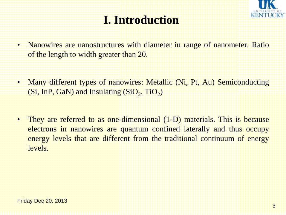
• Nanowires are nanostructures with diameter in range of nanometer. Ratio
of the length to width greater than 20.
• Many different types of nanowires: Metallic (Ni, Pt, Au) Semiconducting
(Si, InP, GaN) and Insulating (SiO2, TiO2)
• They are referred to as one-dimensional (1-D) materials. This is because
electrons in nanowires are quantum confined laterally and thus occupy
energy levels that are different from the traditional continuum of energy
levels.
I. Introduction
3Friday Dec 20, 2013
4
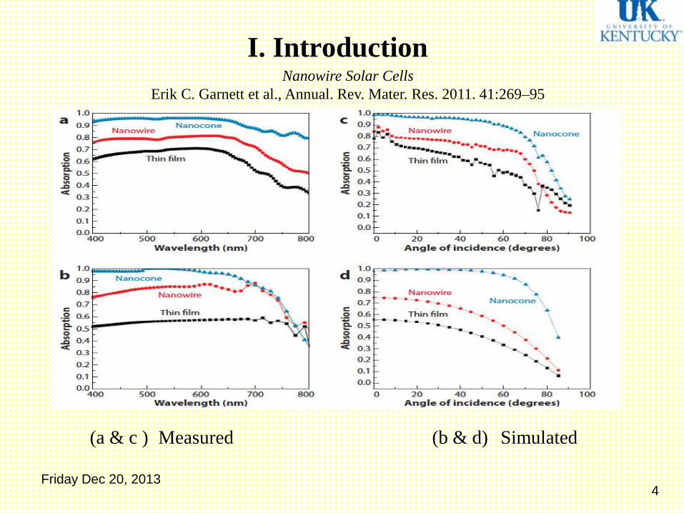
(a & c ) Measured (b & d) Simulated
I. IntroductionNanowire Solar Cells
Erik C. Garnett et al., Annual. Rev. Mater. Res. 2011. 41:269–95
Friday Dec 20, 2013
5
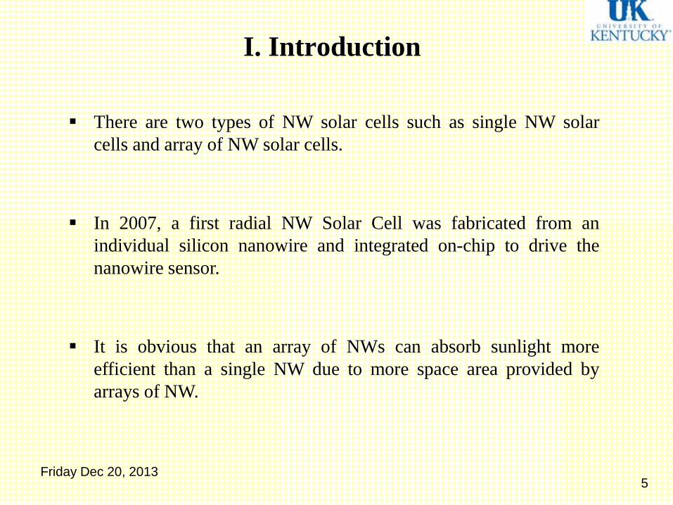
There are two types of NW solar cells such as single NW solar
cells and array of NW solar cells.
In 2007, a first radial NW Solar Cell was fabricated from an
individual silicon nanowire and integrated on-chip to drive the
nanowire sensor.
It is obvious that an array of NWs can absorb sunlight more
efficient than a single NW due to more space area provided by
arrays of NW.
I. Introduction
Friday Dec 20, 2013
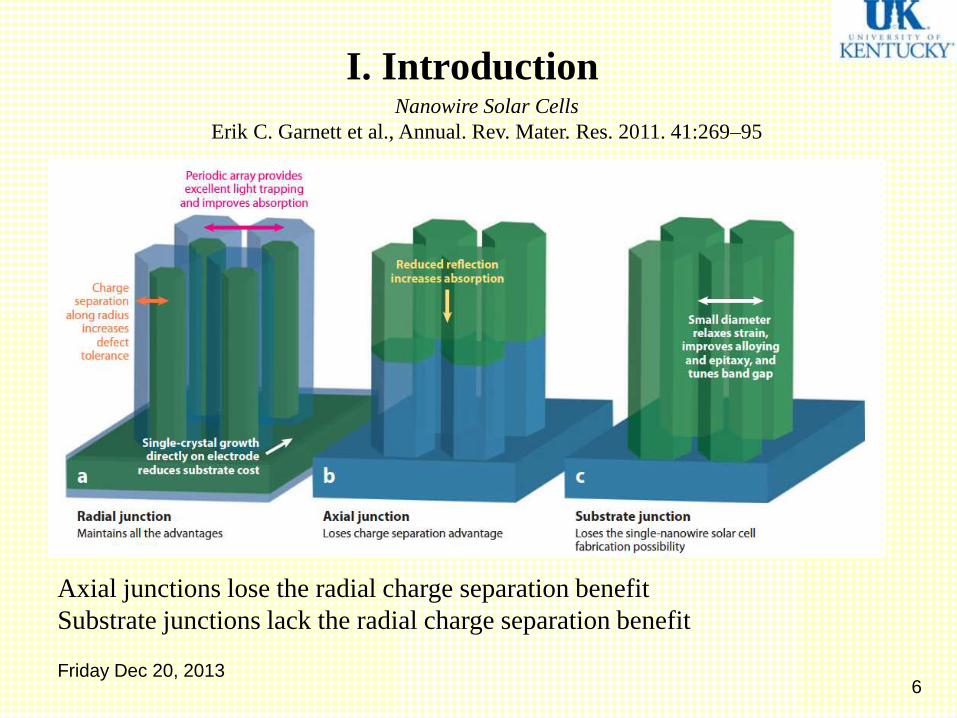
6
Axial junctions lose the radial charge separation benefit
Substrate junctions lack the radial charge separation benefit
I. IntroductionNanowire Solar Cells
Erik C. Garnett et al., Annual. Rev. Mater. Res. 2011. 41:269–95
Friday Dec 20, 2013
7
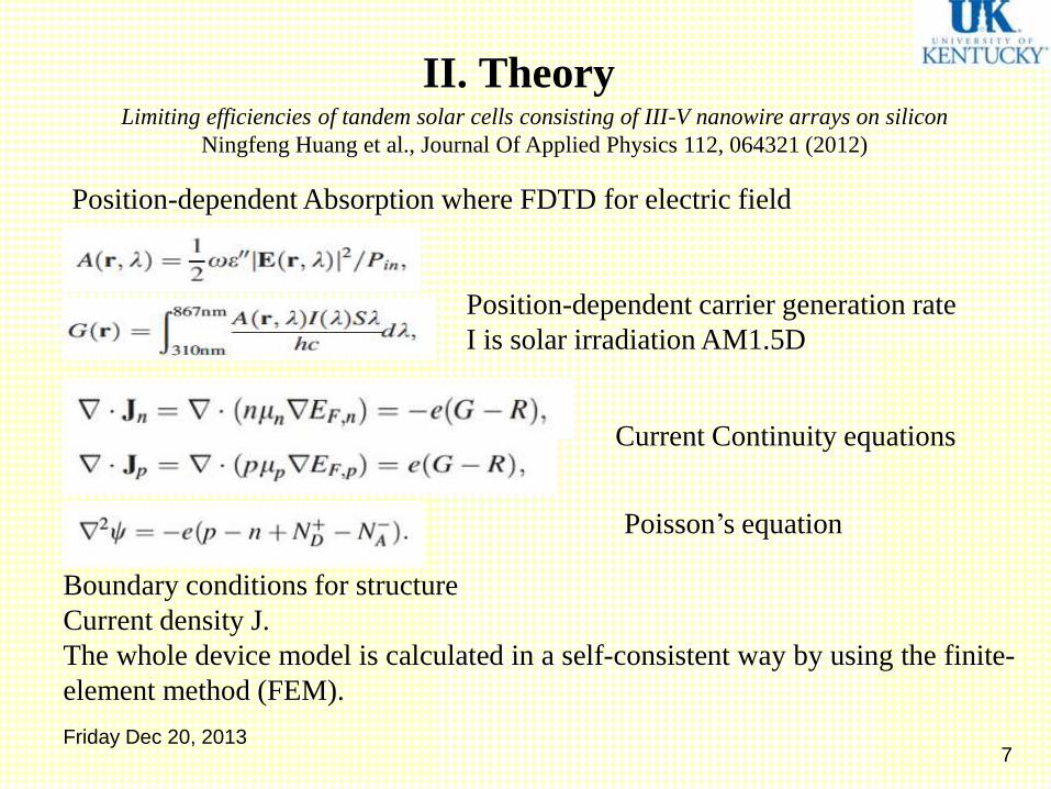
II. Theory
Boundary conditions for structure
Current density J.
The whole device model is calculated in a self-consistent way by using the finite-
element method (FEM).
Limiting efficiencies of tandem solar cells consisting of III-V nanowire arrays on silicon
Ningfeng Huang et al., Journal Of Applied Physics 112, 064321 (2012)
Friday Dec 20, 2013
Position-dependent Absorption where FDTD for electric field
Current Continuity equations
Poisson’s equation
Position-dependent carrier generation rate
I is solar irradiation AM1.5D
8
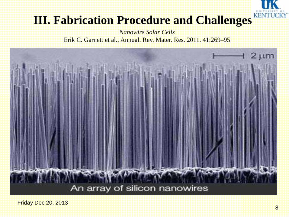
III. Fabrication Procedure and Challenges
Nanowire solar cell fabrication consist of three steps:
Nanowire synthesis
Junction formation
Contacting
Nanowires are commonly grown by vapor-liquid-solid (VLS) process,
electrochemical deposition into nanoporous templates and solution growth.
Two techniques most commonly used in fabrication of nanowire solar cells:
Chemical vapor deposition (CVD)
Patterned chemical etching
Challenge: Large-scale production of the nanowires into highly controlled arrays
with high uniformity.
Nanowire Solar Cells
Erik C. Garnett et al., Annual. Rev. Mater. Res. 2011. 41:269–95
Friday Dec 20, 2013
9
IV. Existing Devices (Design & Performance)
Performance of a solar cell is often measured by factors of Jsc, Voc, and Isc.
In order to improve the performance of NW solar cells a number of new
geometries cross-sections have been recommended for NW SCs.
Circular cross-section
Rectangular cross-section
Triangular cross-section
Hexagonal cross-section
Friday Dec 20, 2013
10
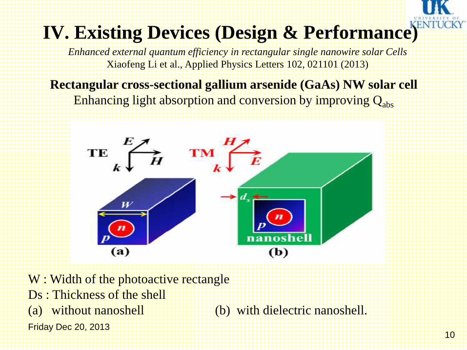
IV. Existing Devices (Design & Performance)
Rectangular cross-sectional gallium arsenide (GaAs) NW solar cell
Enhancing light absorption and conversion by improving Qabs
W : Width of the photoactive rectangle
Ds : Thickness of the shell
(a) without nanoshell (b) with dielectric nanoshell.
Enhanced external quantum efficiency in rectangular single nanowire solar Cells
Xiaofeng Li et al., Applied Physics Letters 102, 021101 (2013)
Friday Dec 20, 2013
11
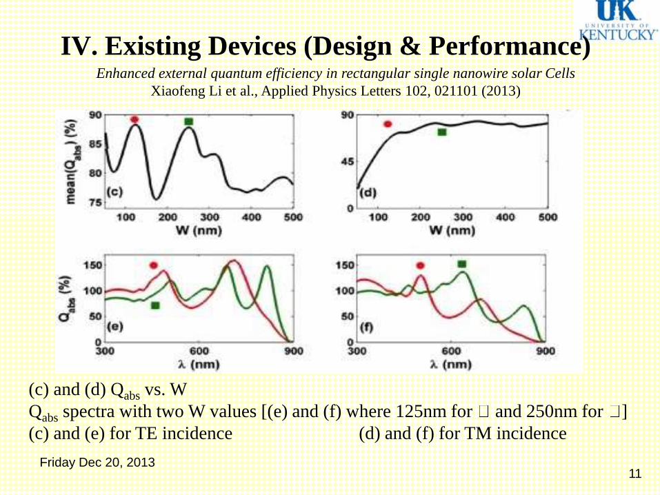
IV. Existing Devices (Design & Performance)
(c) and (d) Qabs vs. W
Qabs spectra with two W values [(e) and (f) where 125nm for and 250nm for ]
(c) and (e) for TE incidence (d) and (f) for TM incidence
Enhanced external quantum efficiency in rectangular single nanowire solar Cells
Xiaofeng Li et al., Applied Physics Letters 102, 021101 (2013)
Friday Dec 20, 2013
12
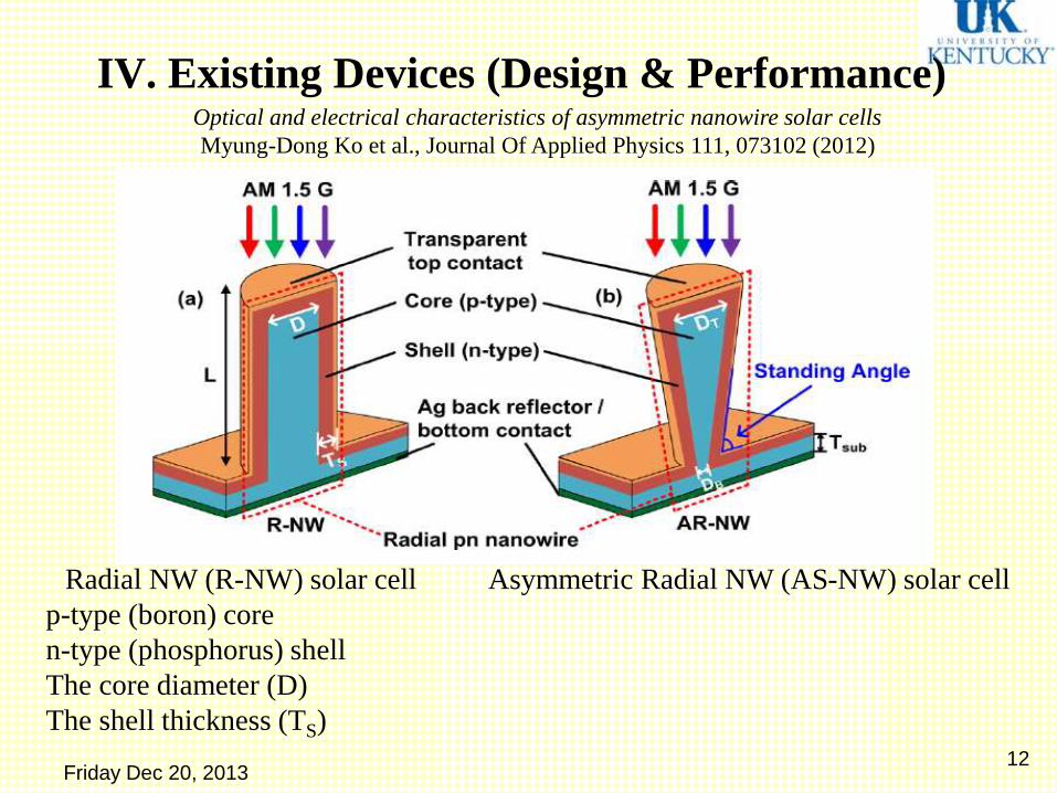
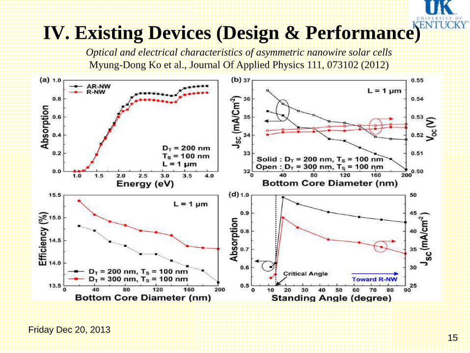
IV. Existing Devices (Design & Performance)Optical and electrical characteristics of asymmetric nanowire solar cells
Myung-Dong Ko et al., Journal Of Applied Physics 111, 073102 (2012)
Radial NW (R-NW) solar cell Asymmetric Radial NW (AS-NW) solar cell
p-type (boron) core
n-type (phosphorus) shell
The core diameter (D)
The shell thickness (TS)
Friday Dec 20, 2013
13
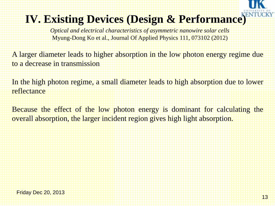
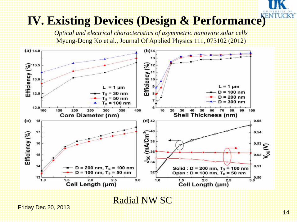
IV. Existing Devices (Design & Performance)
A larger diameter leads to higher absorption in the low photon energy regime due
to a decrease in transmission
In the high photon regime, a small diameter leads to high absorption due to lower
reflectance
Because the effect of the low photon energy is dominant for calculating the
overall absorption, the larger incident region gives high light absorption.
Optical and electrical characteristics of asymmetric nanowire solar cells
Myung-Dong Ko et al., Journal Of Applied Physics 111, 073102 (2012)
Friday Dec 20, 2013
14
IV. Existing Devices (Design & Performance)Optical and electrical characteristics of asymmetric nanowire solar cells
Myung-Dong Ko et al., Journal Of Applied Physics 111, 073102 (2012)
Friday Dec 20, 2013Radial NW SC
15
IV. Existing Devices (Design & Performance)Optical and electrical characteristics of asymmetric nanowire solar cells
Myung-Dong Ko et al., Journal Of Applied Physics 111, 073102 (2012)
Friday Dec 20, 2013
16
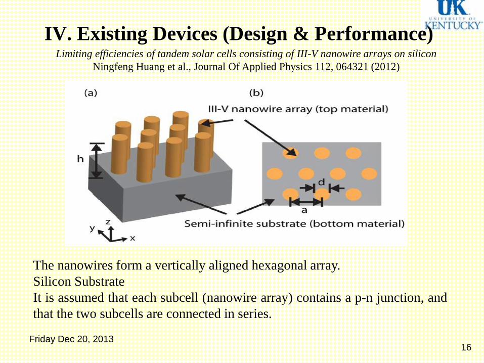
IV. Existing Devices (Design & Performance)Limiting efficiencies of tandem solar cells consisting of III-V nanowire arrays on silicon
Ningfeng Huang et al., Journal Of Applied Physics 112, 064321 (2012)
The nanowires form a vertically aligned hexagonal array.
Silicon Substrate
It is assumed that each subcell (nanowire array) contains a p-n junction, and
that the two subcells are connected in series.
Friday Dec 20, 2013
17
IV. Existing Devices (Design & Performance)Limiting efficiencies of tandem solar cells consisting of III-V nanowire arrays on silicon
Ningfeng Huang et al., Journal Of Applied Physics 112, 064321 (2012)
Considered four different III-V materials for the nanowire array, each with
different band gap energy:
InP 1.34 eV
GaAs 1.43 eV
Al0.2Ga0.8As 1.72 eV
Ga0.5In0.5 P 1.9 eV
The highest limiting efficiency (45.3%) occurs when the band gaps of the top
and bottom subcells are 1.57eV and 0.935eV, respectively.
Friday Dec 20, 2013
18
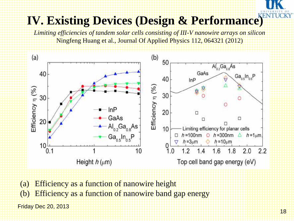
IV. Existing Devices (Design & Performance)Limiting efficiencies of tandem solar cells consisting of III-V nanowire arrays on silicon
Ningfeng Huang et al., Journal Of Applied Physics 112, 064321 (2012)
(a) Efficiency as a function of nanowire height
(b) Efficiency as a function of nanowire band gap energy
Friday Dec 20, 2013
19
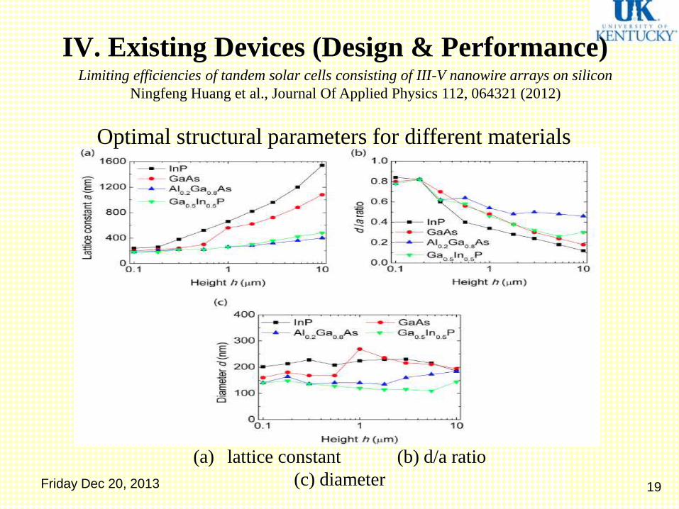
IV. Existing Devices (Design & Performance)Limiting efficiencies of tandem solar cells consisting of III-V nanowire arrays on silicon
Ningfeng Huang et al., Journal Of Applied Physics 112, 064321 (2012)
(a) lattice constant (b) d/a ratio
(c) diameterFriday Dec 20, 2013
Optimal structural parameters for different materials
20
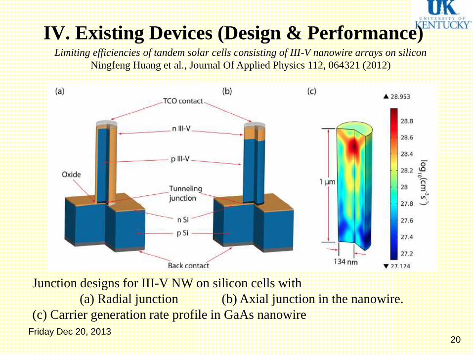
IV. Existing Devices (Design & Performance)Limiting efficiencies of tandem solar cells consisting of III-V nanowire arrays on silicon
Ningfeng Huang et al., Journal Of Applied Physics 112, 064321 (2012)
Junction designs for III-V NW on silicon cells with
(a) Radial junction (b) Axial junction in the nanowire.
(c) Carrier generation rate profile in GaAs nanowire
Friday Dec 20, 2013
21
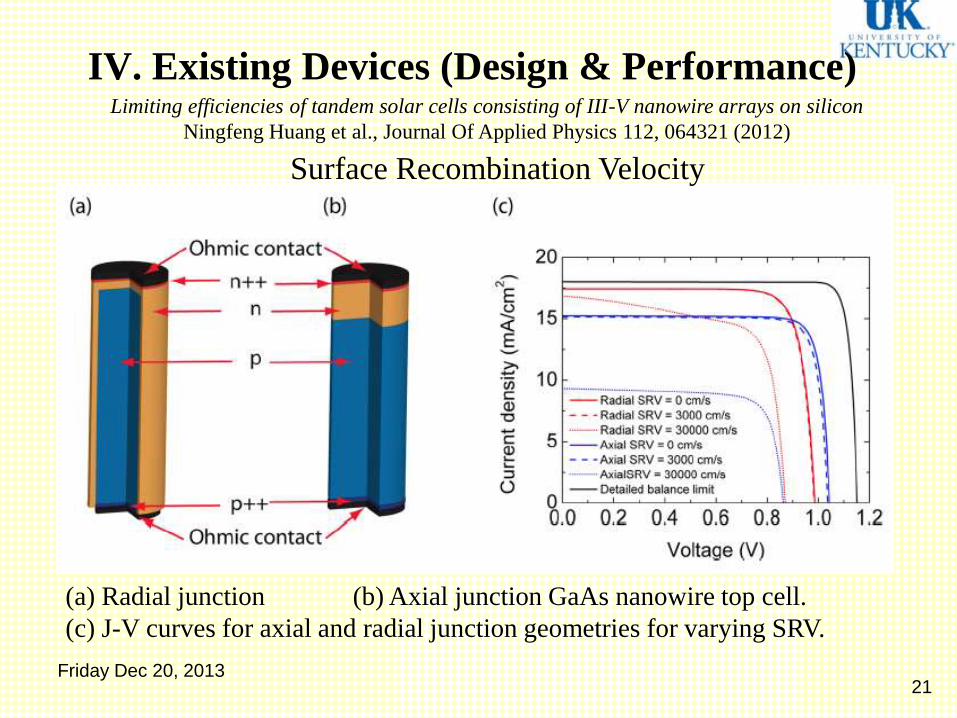
IV. Existing Devices (Design & Performance)Limiting efficiencies of tandem solar cells consisting of III-V nanowire arrays on silicon
Ningfeng Huang et al., Journal Of Applied Physics 112, 064321 (2012)
(a) Radial junction (b) Axial junction GaAs nanowire top cell.
(c) J-V curves for axial and radial junction geometries for varying SRV.
Friday Dec 20, 2013
Surface Recombination Velocity
22
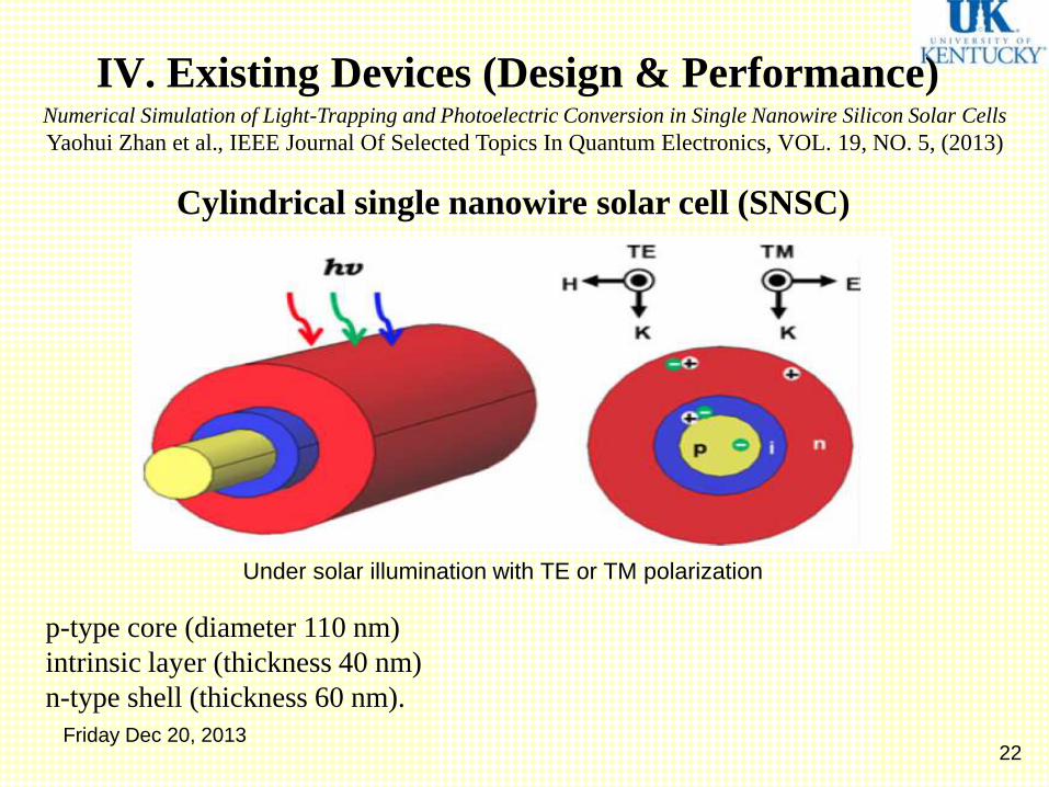
IV. Existing Devices (Design & Performance)Numerical Simulation of Light-Trapping and Photoelectric Conversion in Single Nanowire Silicon Solar Cells
Yaohui Zhan et al., IEEE Journal Of Selected Topics In Quantum Electronics, VOL. 19, NO. 5, (2013)
Cylindrical single nanowire solar cell (SNSC)
Under solar illumination with TE or TM polarization
Friday Dec 20, 2013
p-type core (diameter 110 nm)
intrinsic layer (thickness 40 nm)
n-type shell (thickness 60 nm).
23
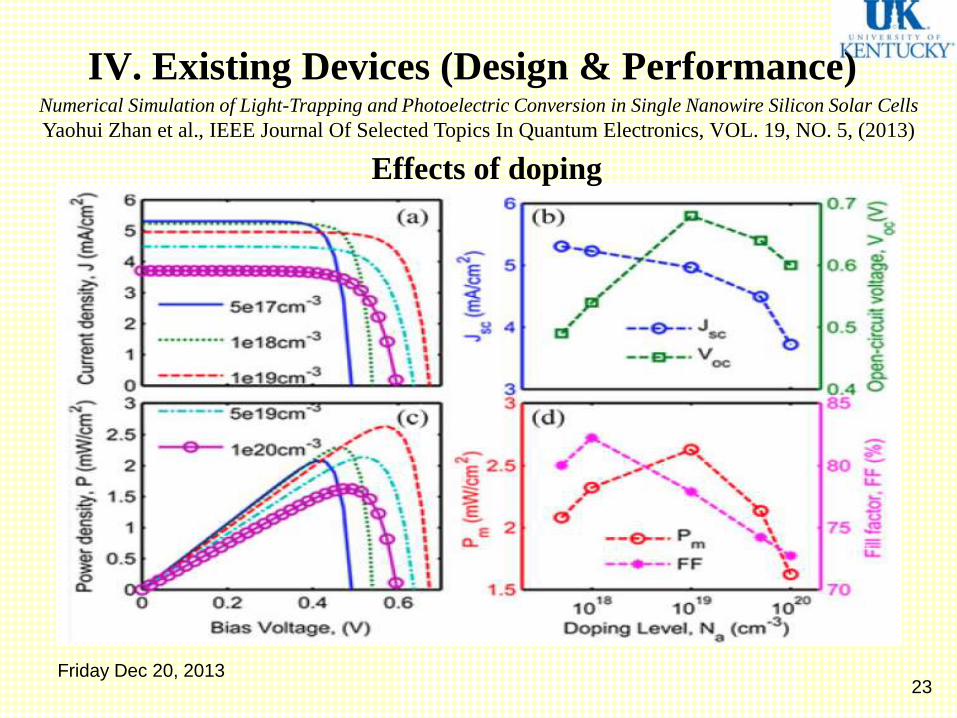
IV. Existing Devices (Design & Performance)
Effects of doping
Friday Dec 20, 2013
Numerical Simulation of Light-Trapping and Photoelectric Conversion in Single Nanowire Silicon Solar Cells
Yaohui Zhan et al., IEEE Journal Of Selected Topics In Quantum Electronics, VOL. 19, NO. 5, (2013)
24
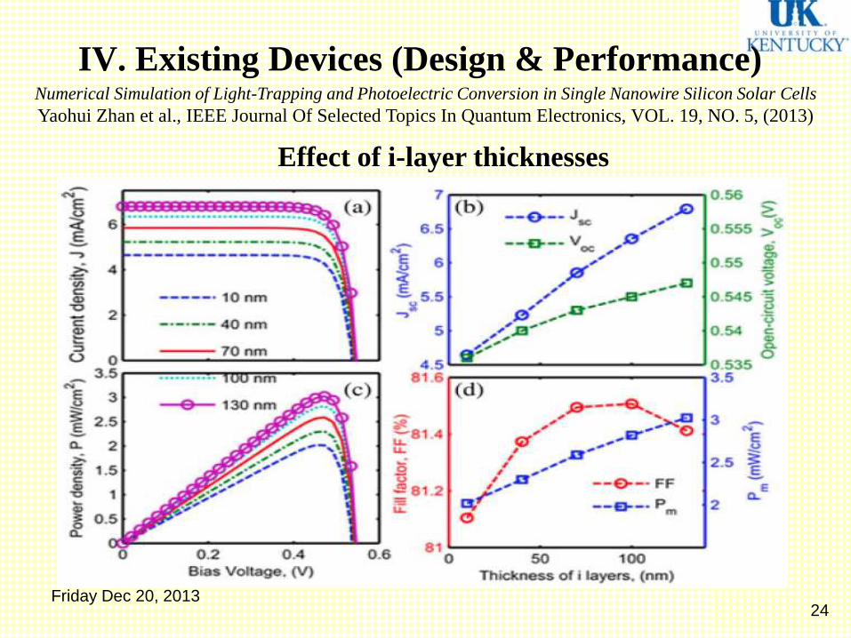
IV. Existing Devices (Design & Performance)
Effect of i-layer thicknesses
Friday Dec 20, 2013
Numerical Simulation of Light-Trapping and Photoelectric Conversion in Single Nanowire Silicon Solar Cells
Yaohui Zhan et al., IEEE Journal Of Selected Topics In Quantum Electronics, VOL. 19, NO. 5, (2013)
25
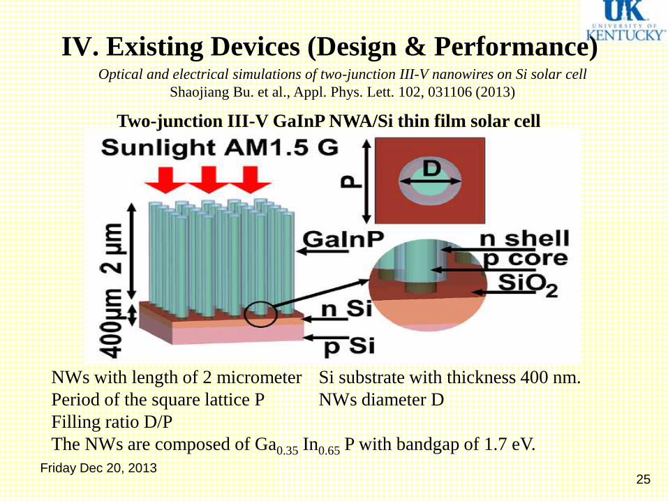
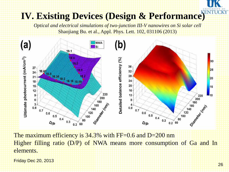
IV. Existing Devices (Design & Performance)Optical and electrical simulations of two-junction III-V nanowires on Si solar cell
Shaojiang Bu. et al., Appl. Phys. Lett. 102, 031106 (2013)
Friday Dec 20, 2013
NWs with length of 2 micrometer Si substrate with thickness 400 nm.
Period of the square lattice P NWs diameter D
Filling ratio D/P
The NWs are composed of Ga0.35 In0.65 P with bandgap of 1.7 eV.
Two-junction III-V GaInP NWA/Si thin film solar cell
26
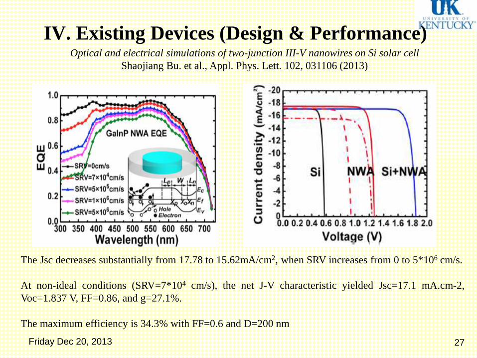
IV. Existing Devices (Design & Performance)Optical and electrical simulations of two-junction III-V nanowires on Si solar cell
Shaojiang Bu. et al., Appl. Phys. Lett. 102, 031106 (2013)
The maximum efficiency is 34.3% with FF=0.6 and D=200 nm
Higher filling ratio (D/P) of NWA means more consumption of Ga and In
elements.
Friday Dec 20, 2013
27
IV. Existing Devices (Design & Performance)Optical and electrical simulations of two-junction III-V nanowires on Si solar cell
Shaojiang Bu. et al., Appl. Phys. Lett. 102, 031106 (2013)
The Jsc decreases substantially from 17.78 to 15.62mA/cm2, when SRV increases from 0 to 5*106 cm/s.
At non-ideal conditions (SRV=7*104 cm/s), the net J-V characteristic yielded Jsc=17.1 mA.cm-2,
Voc=1.837 V, FF=0.86, and g=27.1%.
The maximum efficiency is 34.3% with FF=0.6 and D=200 nm
Friday Dec 20, 2013
28
V. Challenges and Suggestions
NWs Reduce the quantity and quality of material necessary to approach those
limits which allowing for substantial cost reductions.
NWs provide opportunities to fabricate complex single-crystalline
semiconductor devices directly on low-cost substrates and electrodes such as
aluminum foil and conductive glasses.
Many materials relevant to solar cells, including zinc oxide, germanium,
silicon, indium gallium nitride and cadmium sulfide.
Some challenges in the field of nanowire solar cells that include:
Surface and interface recombination
surface roughness
mechanical and chemical stability
doping control
nanowire array uniformity
Friday Dec 20, 2013
29
V. Challenges and Suggestions
Silica substrates will slightly degrade the absorption efficiency of SNSCs,
while metal substrates will greatly enhance the absorption performance.
Rectangular cross section nanowire has the greatest absorption efficiency
among all the geometries
Increase with the number of NW in a parallel array for Jsc
Synthesis methods such as VLS it is possible to very accurately control
nanowire architecture including: size, morphology and material.
As a suggestion:
Multi-junction (two or three multi-junction) nanowire array solar cells with
rectangular geometry on glass or metallic substrates with fabrication methods
such as VLS.
Friday Dec 20, 2013
30
VI. References
1. Shaojiang Bu. et al., Optical and electrical simulations of two-junction III-V nanowires
on Si solar cell, Appl. Phys. Lett. 102, 031106 (2013)
2. Yaohui Zhan et al., Numerical Simulation of Light-Trapping and Photoelectric
Conversion in Single Nanowire Silicon Solar Cells, IEEE Journal Of Selected Topics
In Quantum Electronics, VOL. 19, NO. 5, (2013)
3. Xiaofeng Li et al., Enhanced external quantum efficiency in rectangular single
nanowire solar Cells, Applied Physics Letters 102, 021101 (2013)
4. Myung-Dong Ko et al., Optical and electrical characteristics of asymmetric nanowire
solar cells, Journal Of Applied Physics 111, 073102 (2012)
5. Ningfeng Huang et al., Limiting efficiencies of tandem solar cells consisting of III-V
nanowire arrays on silicon, Journal Of Applied Physics 112, 064321 (2012)
6. Erik C. Garnett et al., Nanowire Solar Cells, Annual. Rev. Mater. Res. 2011. 41:269–95