Nanowires on a Film for Photoelectrochemical WaterSplitting
Miao Zhong, Mario Kurniawan,Aleksandra Apostoluk, Bertrand Vilquin andJean-Jacques Delaunay
Additional information is available at the end of the chapter
http://dx.doi.org/10.5772/52593
1. Introduction
Nanowires-on-a-film structure (NFS) consisting of a dense array of semiconductor nano‐wires on a conductive film has recently attracted much interest due to their wide range ofapplications in electronic, optoelectronic, electromechanic and electrochemical devices [15,5, 25]. Thanks to their 3D geometry, NFSs provide various morphology-induced advantagesresulting in improved devices performances. In addition, as the array of semiconductorNFSs can be grown on a conductive film, which realizes electrical connection between thenanowires, the integration of this nanostructured layer into devices is greatly facilitated.
In this chapter, we review the applications of NFSs as efficient photoanodes in photoelectro‐chemical (PEC) water splitting cells. Recently, the efficiency of the PEC cells has been report‐ed to be enhanced with the use of semiconductor NFSs [23, 10, 30, 32]. The well-alignedgeometry of a nanowire array serves as an anti-reflector in order to enhance light absorptionin the structure. Also, an effective separation of the photo-generated carriers is achievedalong the transverse direction of the nanowires due to the drastically reduced transport dis‐tance of minority carriers. Furthermore, the nanowire array possesses large surface areasthat greatly enhance the chemical reaction of water splitting as compared to its smooth filmcounterpart. Lastly, the underneath film realizes electrical connection between the top nano‐wires. As a consequence, the semiconductor NFS offers a great potential for PEC water split‐ting applications. However, the fabrication of high quality NFS with functionalsemiconductor materials still remains a challenge. Single crystalline functional semiconduc‐
tor materials will ensure the photoanodes to have adequate semiconducting and electro‐chemical properties, leading to fulfill the PEC water splitting requirements [14, 2], including:
• Efficient light absorption
• Effective carrier separation and transport
• Suitable energy band position for redox reaction of water
• Anti-photocorrosive property in the presence of water.
Furthermore, a controllable approach for the fabrication of the NFSs that enables productionof large-area photoanodes at a low cost is not far from being achieved [34].
In the following sections, emphases are placed on the synthesis, property and PEC perform‐ance of the NFSs fabricated using various materials. The materials under review includeTiO2, Fe2O3 and ZnO, as they have the potential to achieve good performance in PEC watersplitting. In addition, surface coating of the ZnO NFS with anti-photocorrosive ZnGa2O4
photocatalyst layer is discussed as a mean to improve the stability of the ZnO based photo‐anodes. Finally, the remaining challenges for the NFS to be used as efficient photoelectrodesfor PEC water splitting are presented. It should be noted that the NFS described here arebased on arrays of one-dimensional (1D) nanowires, however, nanostructured photoanodesbased on nanotubes, nanoplates and other nanostructures on a film should also provide im‐proved PEC device performance.
2. TiO2 NFSs for PEC water splitting
Since the phenomenon of water electrolysis on a titanium dioxide (TiO2) electrode under UVlight illumination was discovered by [9], TiO2 has been considered as one of the most prom‐ising photocatalysts for energy conversion applications. Later in 1977, Frank and Bard ach‐ieved the decomposition of cyanide in water using TiO2 material under UV lightillumination [7]. This achievement further confirmed the photocatalytic behavior of TiO2
material and leaded for the use of TiO2 in environmental and pollution-degradation applica‐tions. Recently, extensive research has been conducted on the TiO2 nanostructures in orderto enhance device performances [3]. Versatile morphologies including TiO2 nanowires,nanosheets, and nanotubes have been fabricated through different chemical and physicalapproaches. In many reports, the vertical alignment of the TiO2 nano-architectures perpen‐dicular to the substrates is found to be a crucial factor necessary to improve device perform‐ances [8, 10]. In this section, we focus on the synthesis, characterizations and PECperformances of TiO2 NFSs.
Nanowires - Recent Advances128
2.1. Synthesis of the TiO2 NFSs
Titanium (Ti) is a relatively refractory metal with a high melting temperature of about 1670°C under air condition. This high melting temperature results in a low Ti vapor pressure of ~10−3 Torr at 1577 °C, which hinders the TiO2 nucleation in the direct Ti vapor-phase deposi‐tion processes such as the physical vapor deposition (PVD) and the thermal chemical vapordeposition (CVD). In order to increase the Ti precursor concentration for the growth of 1DTiO2 nanostructures, hydrothermal growth, sol-gel growth and metal organic chemical va‐por deposition (MOCVD) using Ti organic compounds as precursors are often employed [3].
The fabrication of TiO2 NFS via the hydrothermal growth method has been proved to be ef‐ficient due to its low-temperature processing (which helps to protect the bottom conductivefilm during the growth of 1D nanowires), mass production of the nanowires, and their easi‐ly controllable alignment. As reported by [10], a densely packed, vertically aligned and sin‐gle crystalline TiO2 rutile nanowire array was synthesized on a transparent conductive layerconsisting of fluorine-doped tin oxide (FTO) via the hydrothermal method. The fabricationprocess is described in the following.
The FTO coated glass substrate was first cleaned by sonication in a mixture of ethanol andwater for 30 minutes in order to remove the impurities on the surface of the substrate. Then,a seed layer of TiO2 was synthesized on the cleaned FTO coated glass substrate by a first-step hydrothermal growth. The FTO substrate was soaked in a 0.025 M TiCl4 with n-hexanesolution for 30 minutes. The sample was then rinsed with ethanol and finally annealed at500°C for 30 minutes in air to form a thin layer of TiO2 on the surface of the substrate. Theformation of the TiO2-seeded layer on the FTO substrate improved the control and the integ‐rity of the later TiO2 nanowires growth. Moreover, the TiO2-seeded layer on the FTO layerprevented the formation of electrical short circuits between the electrode and the electrolytewhen used as photoanode in the PEC water splitting cell, which guaranteed the photocata‐lytic function of the TiO2 photoanode. In the next fabrication step, the TiO2 nanowires weregrown on the TiO2-seeded FTO substrate with a typical hydrothermal growth procedure.The seeded FTO substrate was placed in sealed Teflon-lined autoclave containing 50 mL ofn-hexane, 5 mL of HCL and 2.5-5 mL of titanium isopropoxide. After the reaction was per‐formed at 150°C for a certain amount of time, the autoclave was cooled down to room tem‐perature and finally the TiO2 NFS was synthesized.
2.2. Characterization of the TiO2 NFSs
Cross-sectional and top view scanning electron microscope (SEM) images of the synthesizedTiO2 nanowires array are shown in Fig. 1 a and 1b [10]. The TiO2 nanowires array consistingof vertically aligned and tetragonal shaped nanowires is highly uniform and densely packedon the FTO coated glass substrate. The average diameter of the nanowires is ~5 nm and theirlength is up to ~4.5 μm. The length of the nanowires can be tuned from ~0.5 to ~5 μm, bymodifying the synthesis conditions including the precursors ratio (titanium isopropoxide/n-hexane), the reaction time and the thickness of TiO2 seed layer. [10]
Nanowires on a Film for Photoelectrochemical Water Splittinghttp://dx.doi.org/10.5772/52593
The synthesized TiO2 nanowires array was characterized by grazing incidence angle X-raydiffraction (GIXRD) technique as shown in Fig. 1 d. The TiO2 nanowires structure was iden‐tified as a rutile crystal from the reference XRD data measured with standard rutile TiO2
powder. Furthermore, the high resolution transmission electron (HRTEM) image in Fig. 1dshowed that the observed rutile phase TiO2 nanowire is of a single crystal quality, havingclear (110) lattice fringes.
2.3. PEC performance of the TiO2 NFSs
The PEC performance of the synthesized TiO2 NFS (as previously described) was examinedin a three-electrode PEC water splitting cell [10]. The TiO2 NFS was used as the workingelectrode, a saturated Ag/AgCl electrode as the reference electrode and a platinum wire asthe counter electrode. The electrolyte consisted of one mol/liter KOH solution with pH =13.5. For the PEC test, TiO2 nanowires with an average diameter of ~5 nm and averagelength of ~1.5 μm [10] were studied. The linear sweep voltammetry measurement was per‐formed under a 100 W Xenon lamp illumination (300 nm < wavelength λ < 800 nm) with abias swept from -0.8 to 0.6 V (vs. Ag/AgCl), as shown in Fig. 2 a. A photocurrent density of~0.35 mA/cm2 was obtained at a bias of 1.23 VRHE [10].
As reported by Tilley et al. [23, 10], decoration of a photoelectrode with metal nanoparticlesas co-catalysts exhibited an enhanced yield in hydrogen generation. [10], reported treat‐ments by cobalt (Co) and silver (Ag) performed on the TiO2 NFS samples. The photocurrentdensity of ~0.35 mA/cm2 measured on the undoped TiO2 NFS increased to ~0.45 mA/cm2 forthe Co and Ag coated TiO2 NFSs, as shown in Fig. 2 b. The enhancement of the photocurrentafter Co and Ag treatments was likely related to the improvement in the extraction of photo‐generated holes from the surface of the TiO2 NFS to the electrolyte, through the Co and Agnanoparticles [23, 10].
3. Hematite NFS for PEC water splitting
Hematite (α-Fe2O3 or iron oxide) has been widely investigated as a photocatalyst candidatefor PEC water splitting [13, 14, 30] because of its abundance on Earth, its non-toxicity to en‐vironment and its stability in water under light illumination. In addition, a band gap be‐tween 2.1 and 2.2 eV of the hematite enables visible light absorption and thus makes thismaterial promising for water splitting under solar light illumination. However, hematite hasalso some disadvantages such as: small light absorption coefficient, short lifetime of the ex‐cited-state carrier (10-12 s), short hole diffusion length (2-4 nm), inefficient oxygen evolutionreaction kinetics and improper position of the conduction band for hydrogen generation [23,16], limiting the hematite PEC performance. Different research groups made many efforts toaddress these issues [23, 14, 16, 10]. To date, improved performances have been realized inthe following areas:
1. the synthesis of hematite nanostructures to increase the surface areas;
2. the modification of its electronic structure via elemental doping [23, 14, 16, 10] to en‐hance the conductivity;
3. the surface decoration with other co-catalysts to reduce the onset water splitting potential.
Nanowires on a Film for Photoelectrochemical Water Splittinghttp://dx.doi.org/10.5772/52593
131
In the following section, we summarized the results obtained with the silicon-doped hema‐tite nanowire-like array on a conductive film structure (Si-doped NFS-like hematite) deco‐rated with IrO2 nanoparticles [23] for PEC water splitting.
3.1. Synthesis of the Si-doped NFS-like hematite with IrO2 surface decoration
Similarly to titanium, iron (Fe) has a relatively high melting temperature of ~1550 °C underair condition and thus hematite nanostructures growth by simple thermal CVD or PVD usingsolid-phase Fe-compound precursors remains difficult. Instead, solution-phase precursors,such as Fe(CO)5, Fe(AcAc)3 and FeCl3, are used to provide sufficient amount of Fe precur‐sors in the growth phase for the synthesis of hematite nanostructures via atmospheric pres‐sure chemical vapor deposition (APCVD) or hydrothermal growth methods [23, 14, 16, 10].
However, the undoped hematite nanostructure is inactive or very inefficient when used as aphotoanode for PEC water splitting, because of its low conductivity and improper conduc‐tion band position for hydrogen generation. To improve the conductivity, hematite has beendoped by different elements, such as Si, Ti, Sn, Al, Mg and Zn, leading to increase the elec‐tron density. To address the issue of improper conduction band position of hematite, hema‐tite surface decoration treatments with co-catalysts nanoparticles, such as IrO2 nanoparticles[18], were applied to increase the chemical reactions of water oxidation.
As reported by Tilley et al. [23], Si-doped NFS-like hematite sample coated with IrO2 nano‐particles was fabricated and a large photocurrent density of ~3 mA/cm2 was obtained at abias of 1.23 VRHE under AM 1.5 illumination condition. In their synthesis process, a FTO-coated glass was used as the substrate for the NFS growth and put on an aluminum blockheater. The substrate was maintained at 415 °C during the APCVD growth process. The pre‐cursors Fe(CO)5 and tetraethoxysilane (TEOS) were carried to the FTO coated glass substrateby bubbling argon gas at fixed flow rates, calculated to be 3.5 mg/min for Fe(CO)5 and 0.32mg/min for TEOS. These two streams were mixed with an air flow of 2 L/min and verticallysprayed to the substrate. After 5 minutes, NFS-like Si-doped hematite was synthesized. Ac‐cording to Tilley’s reports, the preparation of homogeneous films on large substrates re‐quired a continuously rotating substrate in a rotating belt APCVD reactor. Moreover, theimproved PEC performance with Si-doped NFS-like hematite photoanode needed a firstgrowth of an ultrathin SiO2 interfacial layer of ~1 nm between hematite and FTO. It is verylikely that this silica layer worked as an insulator layer to prevent the current leaking fromthe FTO layer to the electrolyte during the PEC experiments. Finally, the fabricated Si-dopedNFS-like hematite was coated with ~2 nm IrO2 nanoparticles using an electrophoresis depo‐sition process. An increased photocurrent of ~3 mA/cm2 was achieved with the IrO2 nano‐particles coating, to be compared with a photocurrent of ~2 mA/cm2 obtained for the Si-doped NFS-like hematite without co-catalysts [23].
Nanowires - Recent Advances132
3.2. Characterization of the Si-doped NFS-like hematite with IrO2 decoration
The cross-sectional SEM images of the synthesized Si-doped NFS-like hematite are shown inFig. 3 a and 3b [23]. The hematite nanowires with an average height of ~ 500 nm were dense‐ly packed on the FTO-coated glass substrate. The diameter of the hematite nanowires at thetop area varied from 75 to 250 nm. It is observed that the surfaces of hematite nanowireswere very rough and composed of nanoparticles with diameters as small as ~ 10-20 nm. Assuggested by Tilley et al., the rough surfaces further increased the nanowire/electrolyte in‐terface areas and also shortened the diffusion length of the photogenerated holes to the in‐terface areas, contributing to the increase of PEC water splitting performance [23].
Figure 3. Cross-sectional SEM images of the dense and rough Si-doped NSF-like hematite. [23] Copyright John Wileyand Sons.
The microstructure and crystal quality of the NFS-like hematite samples with/without Sidoping were further studied by XRD 2theta-omega scan technique. The XRD results areshown in Fig. 4. [13]. The undoped and Si-doped NFS-like hematite samples did not con‐tain any other iron oxide phases than hematite, indicating a good experimental control overthe hematite synthesis. The fact that the synthesized nanostructures are made of a single-phase hematite is important for the PEC water splitting applications, because other ironoxide phases such as Fe3O4 always contain strong electron-hole recombination centers, thusleading to lifetime degradation of the holes used in the oxidation of water [13]. Anotherimportant feature shown in the XRD results is that the crystal orientation of the synthe‐sized hematite varied with the synthesis conditions. In the case of the undoped NSF-likehematite sample, there is no dominant crystal orientation. The intensities of the different X-ray diffraction peaks obtained with the undoped NSF-like hematite sample (see Fig. 4b) aresimilar to the XRD reference data measured on the randomly oriented hematite powders(see Fig. 4c). In contrast, the Si-doped NFS-like hematite sample showed a clear preferen‐tial [110] crystal orientation. These [110] oriented hematite nanowires likely have an en‐hanced conductivity compared to the randomly oriented hematite nanowires. In fact, theconductivity along the hematite [110] orientation was calculated to be of roughly four or‐ders of magnitude higher than the conductivity along the other crystal orientations perpen‐dicular to the [110] in hematite [12]. Therefore, the Si-doped NFS-like hematite with apreferential [110] orientation reported by Tilley et al. achieved a benchmark high photocur‐rent for PEC water splitting.
Nanowires on a Film for Photoelectrochemical Water Splittinghttp://dx.doi.org/10.5772/52593
Finally, the synthesized Si-doped NFS-like hematite was coated with IrO2 nanoparticles (~2nm in diameter) by the electrophoresis deposition process [23]. The X-ray photoelectronspectroscopy (XPS) results showed an iridium concentration of ~1% on the surface of theIrO2 coated sample, confirming the presence of IrO2 [23].
3.3. PEC performance of the Si-doped NFS-like Hematite with IrO2 decoration
The PEC performance of the IrO2 decorated Si-doped NFS-like hematite was studied using athree-electrode PEC cell [23]. In the reported experiment, the Si-doped NFS-like hematitesample was used as the working electrode, an Ag/AgCl in a saturated KCl solution electrodewas used as the reference electrode and a platinum wire was used as the counter electrode.One mole/liter NaOH solution with pH = 13.6 was used as the electrolyte. The sample wasirradiated with the standard AM1.5 G 100 mW/cm2 solar simulator.
The chrono-amperometry measurement of the hematite photoanode at a bias of 1.23 VRHE
with light on-off cycles shows that an on-off current behavior corresponding to the light on-off cycles is clearly observed (Fig. 5). The low dark current revealed that no/few chemicalreactions occurred on the hematite photoanode without light illumination. A high photocur‐rent density of ~3 mA/cm2 was obtained at a bias of 1.23 VRHE, as shown in Fig. 5. This photo‐current decreased within the 200-second chrono-amperometry scan. As suggested by Tilleyet al., the photocurrent decrease was related to the detachment of the IrO2 nanoparticlesfrom the surfaces of the Si-doped NFS-like hematite due to a weak chemical bonding be‐tween the IrO2 and the hematite. More robust method to attach the IrO2 nanoparticles onhematite should further improve the PEC results, as was suggested by Tilley et al. [23]
Nanowires - Recent Advances134
Figure 5. Chrono-amperometry measuremens of the IrO2 decorated Si-doped NFS-like hematite photoanode at a biasof 1.23 VRHE under AM 1.5 G 100 mW/cm2 light illumination [23] Copyright, John Wiley and Sons.
4. ZnO NFS for PEC water splitting
Due to their unique optoelectronic and semiconducting properties, single crystal ZnOdensely packed nanowire arrays have been intensively studied in the past few decades fortheir potential use in electronic, electromechanical, and photonic devices [29, 20, 5, 26, 4, 32].Recently, much research effort has been devoted to the fabrication of a high quality ZnOnanowire arrays and their application in PEC water splitting with the aim of taking advant‐age of ZnO material properties such as:
1. suitable band edge positions for PEC water splitting and
2. an increased conductivity when compared to TiO2 and hematite for efficient chargetransport [14, 30, 32].
For PEC water splitting applications, an efficient means permitting a good electrical connec‐tion of the nanowires through a conductive film, namely a ZnO NFS, is required. Yang et al.presented a detailed study on the fabrication and PEC performance of ZnO NFS (ZnO nano‐wire arrays on ITO film) with nitrogen doping [30]. An increased PEC photocurrent was ob‐tained with the nitrogen-doped ZnO NFS sample. Wang et al. reported advanced PECperformances with CdS and CdSe quantum dots loaded ZnO NFSs under the conditions ofsacrificial reagents [24]. However promising these results may be, further efforts to increasethe stability of the ZnO NFSs in water under light illumination are required.
Since ZnO is chemically unstable in water under light irradiation, surface coating of the ZnONFS with anti-photocorrosive and photocatalytic shell layers is one of the strategies to im‐prove its chemical stability. However, the search for suitable anti-photocorrosive photocata‐lysts, which can grow easily on the ZnO nanowire surfaces with a high crystal quality, is a
Nanowires on a Film for Photoelectrochemical Water Splittinghttp://dx.doi.org/10.5772/52593
135
major concern. One possible candidate for the shell material is ZnGa2O4. Indeed, ZnGa2O4 isconductive, has anti-photocorrosive ability in water and photocatalytic property for PECwater splitting [11]. In addition, single crystal quality ZnGa2O4 can be synthesized via high-temperature chemical reactions using ZnO as the precursor material. Thus, surface coatingof the ZnO NFS with conductive and anti-photocorrosive ZnGa2O4 shells to form ZnO-ZnGa2O4 core-shell NFS has been investigated [33]. With this structure, stable and efficientwater splitting was achieved [32]. Further improvements are expected, including enhancedvisible light absorption with doping, and efficient charge transfer to the electrolyte with theco-catalyst decoration of the ZnO nanowires.
In this section, we first review the synthesis of high crystal quality ZnO NFSs using differentapproaches. The realization of high quality ZnO nanowire arrays with efficient electricalconnection is crucial for their subsequent use in high performance PEC cells. Then, the sur‐face coating of the anti-photocorrosive ZnGa2O4 shells on the ZnO NFS is presented. Finally,the electronic properties and a stable PEC performance of the single crystal ZnO-ZnGa2O4
core-shell NFS are reported in detail.
4.1. Synthesis of the ZnO NFSs
A variety of physical and chemical approaches have been used to synthesize dense and sin‐gle crystal ZnO nanowire arrays, including laser interference lithography [27], template-as‐sisted wet-chemical growth [30, 4], MOCVD [21] and CVD [29, 5, 34]. As evidenced by thesereports, the choice of a suitable substrate is of highest importance to synthesize single crystalZnO nanowires with an aligned geometry.
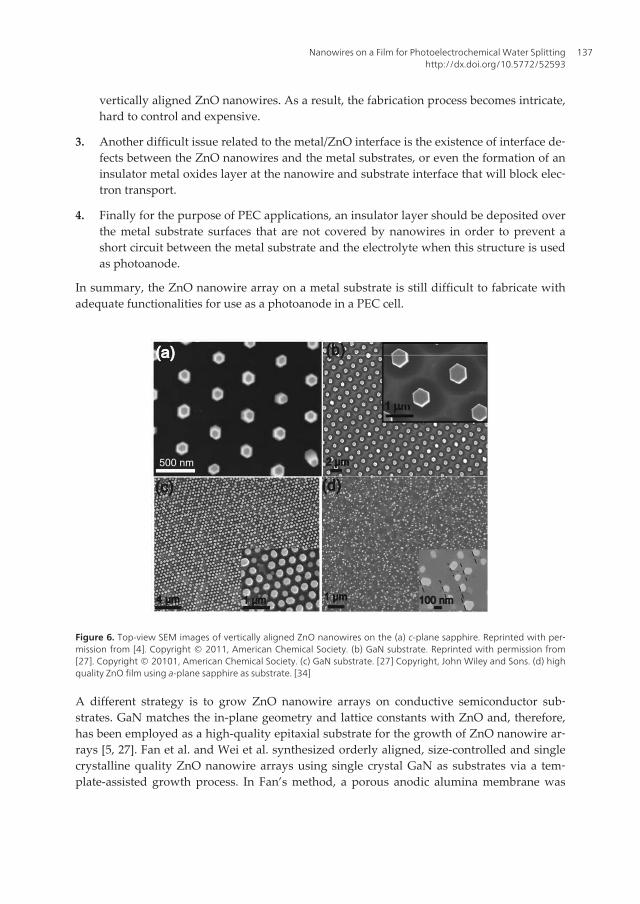
Sapphire is a chemically stable and relatively cheap ceramic material and thus has beenwidely used as substrates for the growth of ZnO nanowire arrays in various fabricationprocesses. Erdélyi, et al. reported the synthesis of a single crystal quality and mono-orientedZnO nanowire array on a c-plane sapphire by the pulsed laser deposition [4]. In their experi‐ment, the pre-growth of a high quality and size controlled ZnO nanoseeds is needed for thegrowth of the nanowires. The top-view SEM image of the ZnO nanowire array is shown inFig. 6 a. Because sapphire is an insulator, the as-grown ZnO nanowires on the sapphire sub‐strate are not electrically connected, preventing their efficient use in optoelectronic applica‐tions. Thus, high quality ZnO nanowire arrays grown on conductive films are a prerequisiteto the development of advanced nanowire-based materials.
One strategy is to form ZnO NFS on metal substrates. However, the growth of nanowires onmetal substrate presents many difficulties. Three major issues should be addressed to realizethe functionality of the ZnO NFS using metal substrates. They are as follows:
1. In order to avoid the formation of a Schottky barrier at the interfaces between the ZnOnanowires and the metal substrate, the work function of the metal should be lower thanthe Fermi level of the ZnO. This requirement severely limits the possible candidates forthe metal substrates.
2. Metal substrates usually have large lattice mismatches with ZnO and, therefore, a pre-growth of lattice matched ZnO nanoseeds on the metal substrate is necessary to obtain
Nanowires - Recent Advances136
vertically aligned ZnO nanowires. As a result, the fabrication process becomes intricate,hard to control and expensive.
3. Another difficult issue related to the metal/ZnO interface is the existence of interface de‐fects between the ZnO nanowires and the metal substrates, or even the formation of aninsulator metal oxides layer at the nanowire and substrate interface that will block elec‐tron transport.
4. Finally for the purpose of PEC applications, an insulator layer should be deposited overthe metal substrate surfaces that are not covered by nanowires in order to prevent ashort circuit between the metal substrate and the electrolyte when this structure is usedas photoanode.
In summary, the ZnO nanowire array on a metal substrate is still difficult to fabricate withadequate functionalities for use as a photoanode in a PEC cell.
A different strategy is to grow ZnO nanowire arrays on conductive semiconductor sub‐strates. GaN matches the in-plane geometry and lattice constants with ZnO and, therefore,has been employed as a high-quality epitaxial substrate for the growth of ZnO nanowire ar‐rays [5, 27]. Fan et al. and Wei et al. synthesized orderly aligned, size-controlled and singlecrystalline quality ZnO nanowire arrays using single crystal GaN as substrates via a tem‐plate-assisted growth process. In Fan’s method, a porous anodic alumina membrane was
Nanowires on a Film for Photoelectrochemical Water Splittinghttp://dx.doi.org/10.5772/52593
137
used as a template mask to control the gold catalysts deposition on the GaN substrate,whereas in Wei’s method, laser interference lithography technique was used for a pre-growth of high quality ZnO nanoseeds on the GaN substrate. According to their reports, thediameters and distributions of the synthesized ZnO nanowires are governed by the parame‐ters of the porous alumina membrane and the laser interference lithography techniques, re‐spectively. The top-view SEM images of the synthesized ZnO nanowires are shown in Fig 6b and 6c. Advanced piezo-electric performances have been reported for the fabricated ZnONFSs. For the use in PEC applications, special attention should be paid to the interface de‐fects and the barrier formation between the ZnO and the GaN in order to realize an efficientelectrical charge collection.
The fabrication of a high quality ZnO nanowire array on a ZnO film (ZnO NFS) using a sin‐gle-step CVD process has been recently reported by our group [34]. The synthesis processenables the growth of a dense ZnO nanowires array on a ZnO film. The nanowires, as wellas the film, have a single crystal domain texture quality and the nanowires are perfectlyaligned over a large area, which comes as the result of the single crystal domain texture. Thetop-view SEM image of the fabricated array is shown in Fig 6 d. Efficient electrical connec‐tion is realized because nanowires and the underneath film layer are made of the same ma‐terial ZnO [34]. Compared to other growth processes of ZnO NFSs, our one-step CVDprocess is easily controlled and cheap. However, the diameters and distributions of the ZnOnanowires cannot be as precisely controlled as in the template-assisted growth processes.The synthesized ZnO NFS offers an ideal template for the subsequent synthesis of a singlecrystal ZnO-ZnGa2O4 core-shell NFS, which provides anti-photocorrosive property for thePEC applications.
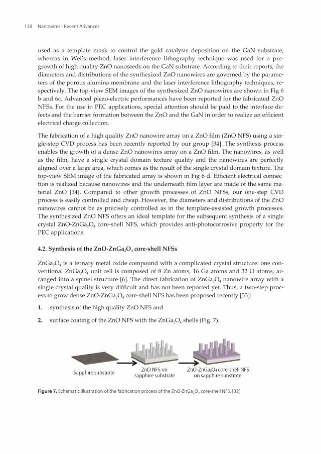
4.2. Synthesis of the ZnO-ZnGa2O4 core-shell NFSs
ZnGa2O4 is a ternary metal oxide compound with a complicated crystal structure: one con‐ventional ZnGa2O4 unit cell is composed of 8 Zn atoms, 16 Ga atoms and 32 O atoms, ar‐ranged into a spinel structure [6]. The direct fabrication of ZnGa2O4 nanowire array with asingle crystal quality is very difficult and has not been reported yet. Thus, a two-step proc‐ess to grow dense ZnO-ZnGa2O4 core-shell NFS has been proposed recently [33]:
1. synthesis of the high quality ZnO NFS and
2. surface coating of the ZnO NFS with the ZnGa2O4 shells (Fig. 7).
Figure 7. Schematic illustration of the fabrication process of the ZnO-ZnGa2O4 core-shell NFS. [32]
Nanowires - Recent Advances138
A high quality ZnO NFS consisting of dense and vertically aligned nanowires on the ZnOfilm was first fabricated using an a-plane sapphire substrate through a simple thermal CVDprocess [32]. In this process, Au-coated a-plane sapphire was selected as the growth sub‐strate. ZnO powder and graphite powder mixed with a 2:1 weight ratio were used as sourcematerial and placed at 1 cm upstream position away from the substrate in a tubular furnace.The furnace was operated at 1000 ºC for 30 minutes with the argon and oxygen gas mixture(5:1 in volume ratio) flowing through the tube at the working pressure of 50 mbar. At theend of the synthesis, the furnace cooled down naturally to the room temperature. The syn‐thesized product consisted of a dense nanowires array on a ZnO film (ZnO NFS). Such astructure offers several advantages, namely,
1. the ZnO nanowires grown on the ZnO film are less prone to the formation of defects atthe interface between the nanowires and the film and thus an efficient electrical connec‐tion of the ZnO nanowires is realized;
2. the underneath ZnO film is stable at high temperature, which enables the subsequentgrowth of the ZnGa2O4 shells in the second CVD step, without damaging the NFS.
In a second step, a CVD growth was performed on the ZnO NFS sample. The sample wasput in a furnace at a temperature of 900ºC. Mixed precursors of Ga2O3, ZnO and graphitewere placed at 11 cm upstream position from the sample. The temperature of the precursorzone was set to 1180 ºC. The carrier gases consisted of the argon and oxygen (10:1 in volumeratio) at the working pressure of 50 mbar. After a 30 minutes-long growth, the ZnO-ZnGa2O4 core-shell NFS was obtained [32].
4.3. Characterization of ZnO-ZnGa2O4 core-shell NFSs
The morphologies of the synthesized ZnO and ZnO-ZnGa2O4 core-shell NFSs are presentedin Fig. 8. The tilted-angle SEM image of Fig. 8a shows a highly uniform and densely ZnOnanowire array grown over a large area on the Au-coated a-plane sapphire substrate. Theinset in Fig. 8a is an enlarged SEM image revealing the vertically aligned nanowires. Thevertical alignment and smooth sidewalls of the nanowires can be clearly observed. The aver‐age diameter of the nanowires is ~70 nm and the average length is about 1 μm. Energy-dis‐persive X-ray analyses (EDX) performed on the nanowire array gave a Zn/O atomic ratio of~1/1, indicating the formation of the ZnO nanowires [34].
The tilted-angle SEM image of Fig. 8b shows a densely packed array of ZnO-ZnGa2O4 core-shell nanowires homogeneously arranged over large areas. The inset in Fig. 8b is an en‐larged SEM image of the vertically aligned ZnO-ZnGa2O4 core-shell nanowires. The initialvertical alignment of the ZnO nanowires is well maintained in the ZnO-ZnGa2O4 core-shellnanowire sample. The average diameter of the ZnO-ZnGa2O4 core-shell nanowires is ~100nm. EDX analysis performed on the surfaces of the core-shell nanowire gave a Zn/Ga/Oatomic ratio of ~14/28/58 (~1/2/4), indicating the formation of the ZnGa2O4 shells. [32] In thiswork, a nanowires-on-a-film structure
Nanowires on a Film for Photoelectrochemical Water Splittinghttp://dx.doi.org/10.5772/52593
139
Figure 8. Tilted-angle SEM image of the dense and vertically aligned (a) ZnO and (b) ZnO-ZnGa2O4 nanowire arrays onthe a-plane sapphire substrate. Insets in (a) and (b) are close-up images of the vertically aligned ZnO and ZnO-ZnGa2O4
nanowires. [32 and 34]
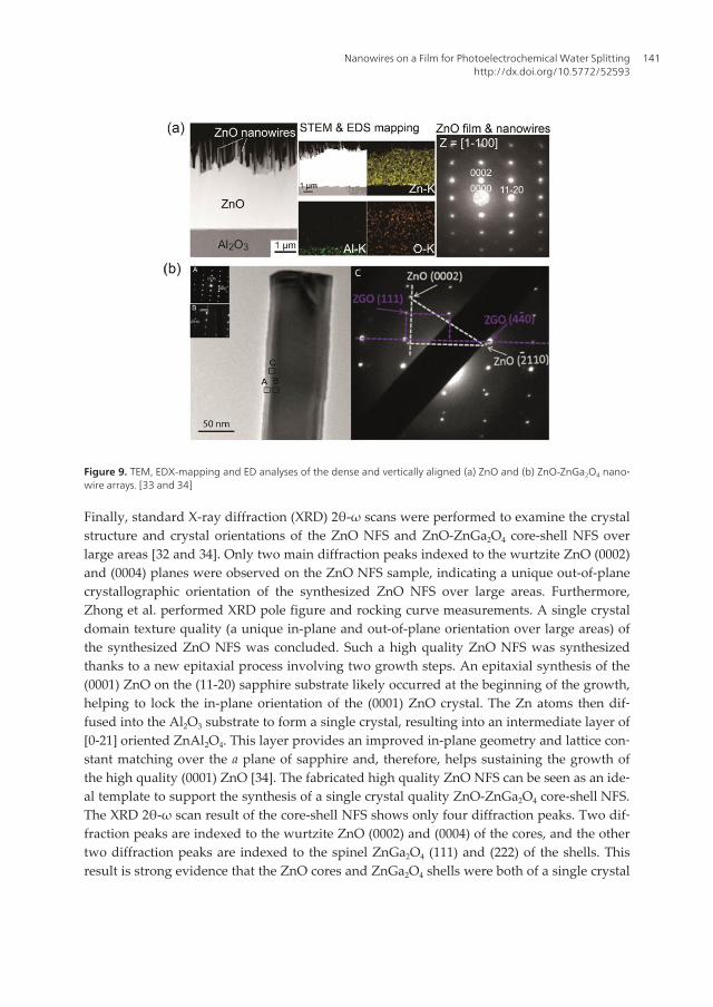
TEM and electron diffraction (ED) were used to analyze the structure and the crystalline qualityof the ZnO and ZnO-ZnGa2O4 core-shell NFSs. The cross-sectional high-angle annular dark-field (HAADF) TEM image of the ZnO NFS is shown in Fig. 9a (left image). The average lengthof the nanowires is about 1 μm and the thickness of the film is about 2.5 μm. Such a thick ZnObottom layer realized the electrical connection of the nanowire array. The energy dispersivespectroscopy (EDS) mapping images presented in Fig. 9a (the central image) clearly revealthat the NFS is made of ZnO and fabricated on the a-plane sapphire substrate.
ED analyses were further performed to characterize the crystal quality and the crystallo‐graphic orientation of the ZnO NFS sample. The ED pattern with the incident zone axis of[1-100] (see the right image in Fig. 9a) shows that the ZnO nanowire array and ZnO thickfilm are all single crystalline and well-aligned along the wurtzite [0001] direction. Such asingle crystal and unique [0001] oriented ZnO NFS offers an ideal substrate for the subse‐quent growth of the ZnO-ZnGa2O4 core-shell NFS.
The TEM and ED results of the ZnO-ZnGa2O4 core-shell NFS are shown in Fig. 9b [33]. Thebright-field TEM image reveals the nanowire core-shell structure with a different brightnesscontrast. The ED pattern of the shell region marked as the square A in the fig. 9b presented inthe inset A of this figure shows that the shell part of the nanowire consists of a single-crystal‐line spinel ZnGa2O4 with a [111] direction parallel to the long axial direction of the nano‐wire. The ED pattern of the core region of B (square B, the ED pattern is shown in the inset B)confirms that the core part of the nanowire is a single crystal wurtzite ZnO with a [0002]direction parallel to the long axial direction of the nanowire. Furthermore, the ED pattern takenon the interfacial region of C (square C, the ED pattern is shown in the inset C) clearly showstwo sets of single-crystalline electron diffraction dot patterns, indexed to the spinel ZnGa2O4
and the wurtzite ZnO. From the electron diffraction pattern, it is found that the ZnGa2O4 [111]direction is parallel to the ZnO [0002] direction and the ZnGa2O4 [2-20] direction is parallel tothe ZnO [-2110] direction. An epitaxial relationship between the ZnGa2O4 (11-2) plane and theZnO (1-100) plane is therefore predicted. Thus the subsequent growth of ZnGa2O4 on the ZnONFS results in a hetero-epitaxial growth of the ZnGa2O4 shells on the ZnO cores. The finalproduct is well-aligned ZnO-ZnGa2O4 core-shell nanowires.
Nanowires - Recent Advances140
Figure 9. TEM, EDX-mapping and ED analyses of the dense and vertically aligned (a) ZnO and (b) ZnO-ZnGa2O4 nano‐wire arrays. [33 and 34]
Finally, standard X-ray diffraction (XRD) 2θ-ω scans were performed to examine the crystalstructure and crystal orientations of the ZnO NFS and ZnO-ZnGa2O4 core-shell NFS overlarge areas [32 and 34]. Only two main diffraction peaks indexed to the wurtzite ZnO (0002)and (0004) planes were observed on the ZnO NFS sample, indicating a unique out-of-planecrystallographic orientation of the synthesized ZnO NFS over large areas. Furthermore,Zhong et al. performed XRD pole figure and rocking curve measurements. A single crystaldomain texture quality (a unique in-plane and out-of-plane orientation over large areas) ofthe synthesized ZnO NFS was concluded. Such a high quality ZnO NFS was synthesizedthanks to a new epitaxial process involving two growth steps. An epitaxial synthesis of the(0001) ZnO on the (11-20) sapphire substrate likely occurred at the beginning of the growth,helping to lock the in-plane orientation of the (0001) ZnO crystal. The Zn atoms then dif‐fused into the Al2O3 substrate to form a single crystal, resulting into an intermediate layer of[0-21] oriented ZnAl2O4. This layer provides an improved in-plane geometry and lattice con‐stant matching over the a plane of sapphire and, therefore, helps sustaining the growth ofthe high quality (0001) ZnO [34]. The fabricated high quality ZnO NFS can be seen as an ide‐al template to support the synthesis of a single crystal quality ZnO-ZnGa2O4 core-shell NFS.The XRD 2θ-ω scan result of the core-shell NFS shows only four diffraction peaks. Two dif‐fraction peaks are indexed to the wurtzite ZnO (0002) and (0004) of the cores, and the othertwo diffraction peaks are indexed to the spinel ZnGa2O4 (111) and (222) of the shells. Thisresult is strong evidence that the ZnO cores and ZnGa2O4 shells were both of a single crystal
Nanowires on a Film for Photoelectrochemical Water Splittinghttp://dx.doi.org/10.5772/52593
141
quality and that the crystallographic axes of [0001] ZnO and [111] ZnGa2O4 are well alignedover large areas.
4.4. Electronic properties of ZnO-ZnGa2O4 core-shell NFSs
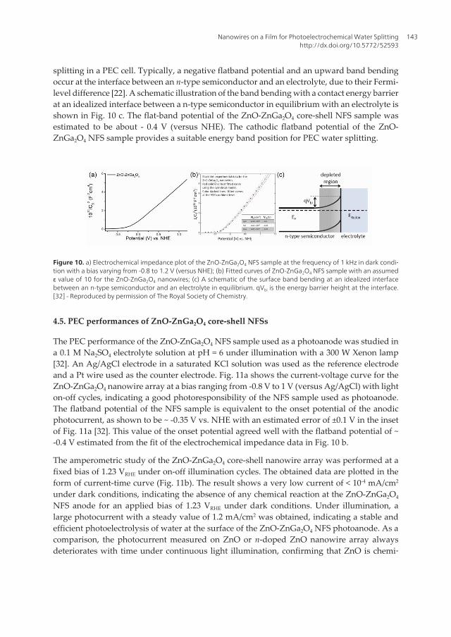
It is of first importance for the development of PEC water splitting cells to understand theelectronic properties of the ZnO-ZnGa2O4 core-shell NFS photoanode in the electrolyte solu‐tion. The carrier density and the flatband potential of the ZnO-ZnGa2O4 core-shell NFS weremeasured by electrochemical impedance spectroscopy [32]. For this purpose, a solution of0.5 M NaClO4 buffered (pH of 7.0) was used as an electrolyte, Ag/AgCl electrode in saturat‐ed KCl solution as the reference electrode, a Pt wire as the counter electrode and the ZnO-ZnGa2O4 core-shell NFS sample as a working electrode. Prior to the electrochemicalimpedance measurement, N2 gas was bubbled for 10 minutes to get rid of O2 in the electro‐lyte solution. The electrochemical impedance analysis was then performed for a bias rang‐ing from - 1 to 1 V (versus Ag/AgCl), at the frequency of 1 kHz under dark condition. Theresults of this experiment are presented in a 1/C 2 vs. V plot (Fig. 10a).
The carrier density and the flatband potential of the cylindrical nanowires were quantifiedusing the model proposed by [17]. Solving the Poisson equation with a cylindrical capaci‐tance approximation at the nanowire/electrolyte interfaces, we obtain:
0
1d
V qr N
r r r ee
¶ ¶= -
¶ 
æ öç ÷è ø
(1)
2
0
2 2
2
( )S
xC
R R x
ee=
-(2)
where R is the radius of the nanowires, x the central radius of the quasi-neutral region in thenanowires, C S the capacitance per unit area of the nanowires, V the applied bias betweenthe electrodes, V FB the flatband potential of the nanowire at the nanowire/electrolyte inter‐face, q the unit electron charge, ε 0 the permittivity of vacuum and ε the relative dielectricconstant of ZnO. The results of the fitting of the measured 1/C 2 vs. V curve according to theMora-Seró model are shown in Fig. 10 b. The carrier density of the ZnO-ZnGa2O4 nanowireswas estimated to be ~1019 cm-3. According to the literature [1, 28, 34], the carrier density ofthe undoped ZnO nanowires is usually around ~1017 – 1018 cm-3. The increase in the carrierdensity of the ZnO-ZnGa2O4 NFS sample compared to that of the ZnO nanowires can be un‐derstood as the formation of conductive ZnGa2O4 shell layers and the introduction of Ga do‐nors inside the ZnO cores [19, 31]. The increased carrier density in the ZnO-ZnGa2O4
nanowires decreases their electrical resistance and thus contributes to a reduced energy lossfor PEC water splitting applications.
The flatband potential of the ZnO-ZnGa2O4 NFS sample at the nanowire/electrolyte inter‐face is another important parameter when analyzing the photoanodes properties for water
Nanowires - Recent Advances142
splitting in a PEC cell. Typically, a negative flatband potential and an upward band bendingoccur at the interface between an n-type semiconductor and an electrolyte, due to their Fermi-level difference [22]. A schematic illustration of the band bending with a contact energy barrierat an idealized interface between a n-type semiconductor in equilibrium with an electrolyte isshown in Fig. 10 c. The flat-band potential of the ZnO-ZnGa2O4 core-shell NFS sample wasestimated to be about - 0.4 V (versus NHE). The cathodic flatband potential of the ZnO-ZnGa2O4 NFS sample provides a suitable energy band position for PEC water splitting.
Figure 10. a) Electrochemical impedance plot of the ZnO-ZnGa2O4 NFS sample at the frequency of 1 kHz in dark condi‐tion with a bias varying from -0.8 to 1.2 V (versus NHE); (b) Fitted curves of ZnO-ZnGa2O4 NFS sample with an assumedε value of 10 for the ZnO-ZnGa2O4 nanowires; (c) A schematic of the surface band bending at an idealized interfacebetween an n-type semiconductor and an electrolyte in equilibrium. qVbi is the energy barrier height at the interface.[32] - Reproduced by permission of The Royal Society of Chemistry.
4.5. PEC performances of ZnO-ZnGa2O4 core-shell NFSs
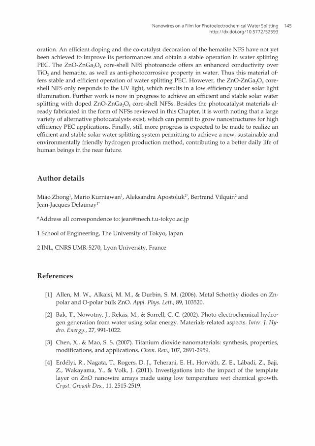
The PEC performance of the ZnO-ZnGa2O4 NFS sample used as a photoanode was studied ina 0.1 M Na2SO4 electrolyte solution at pH = 6 under illumination with a 300 W Xenon lamp[32]. An Ag/AgCl electrode in a saturated KCl solution was used as the reference electrodeand a Pt wire used as the counter electrode. Fig. 11a shows the current-voltage curve for theZnO-ZnGa2O4 nanowire array at a bias ranging from -0.8 V to 1 V (versus Ag/AgCl) with lighton-off cycles, indicating a good photoresponsibility of the NFS sample used as photoanode.The flatband potential of the NFS sample is equivalent to the onset potential of the anodicphotocurrent, as shown to be ~ -0.35 V vs. NHE with an estimated error of ±0.1 V in the insetof Fig. 11a [32]. This value of the onset potential agreed well with the flatband potential of ~-0.4 V estimated from the fit of the electrochemical impedance data in Fig. 10 b.
The amperometric study of the ZnO-ZnGa2O4 core-shell nanowire array was performed at afixed bias of 1.23 VRHE under on-off illumination cycles. The obtained data are plotted in theform of current-time curve (Fig. 11b). The result shows a very low current of < 10-4 mA/cm2
under dark conditions, indicating the absence of any chemical reaction at the ZnO-ZnGa2O4
NFS anode for an applied bias of 1.23 VRHE under dark conditions. Under illumination, alarge photocurrent with a steady value of 1.2 mA/cm2 was obtained, indicating a stable andefficient photoelectrolysis of water at the surface of the ZnO-ZnGa2O4 NFS photoanode. As acomparison, the photocurrent measured on ZnO or n-doped ZnO nanowire array alwaysdeteriorates with time under continuous light illumination, confirming that ZnO is chemi‐
Nanowires on a Film for Photoelectrochemical Water Splittinghttp://dx.doi.org/10.5772/52593
143
cally unstable in water under illumination (Li et al. 2009). After switching off the light illu‐minating the ZnO-ZnGa2O4 NFS anode, a fast recovery of the current to the dark currentvalue was clearly observed. The on-off current cycles presented a very good reproducibilityand anti-photocorrosion stability as shown in Fig. 11 b. Therefore, the core-shell NFS dem‐onstrated an improved stability and a large photocurrent of 1.2 mA/cm2 when used as thephotoanode in the PEC water splitting cell [32].
Figure 11. a) Current-voltage curves of the ZnO-ZnGa2O4 NFS sample in an electrolyte of 0.1 M Na2SO4 at pH = 6 underillumination with a 300 W Xenon lamp. Sweep rate of the voltage was 0.5 mV/s. (b) Current-time curve of the ZnO-ZnGa2O4 NFS when used as a photoanode at an applied bias of 1.23 VRHE with light on-off cycles. [32] - Reproduced bypermission of The Royal Society of Chemistry.
5. Conclusions
Recent advances in the development of densely packed and single crystalline quality semi‐conductor NFSs with a controllable doping level offer promising opportunities for the fu‐ture PEC water splitting applications. In this type of nanostructured photoanodes, animproved light absorption, enhanced charge separation and an increased surface area forchemical reaction are obtained due to the shell layer of the semiconductor nanowire array ofthe NFS. Further, the film underneath the nanowires realizes an efficient electrical connec‐tion of the semiconductor nanowire array, thus facilitating the direct use of the NFS as thephotoanode in PEC water splitting applications. However, many difficulties still remain tobe resolved. Two essential issues related to the reliability and the efficiency needs to be ad‐dressed for all the PEC water splitting systems. In this Chapter, the NFS-based photoanodesmade of different semiconductor photocatalysts have been reviewed and their advantagesand the remaining challenges have been discussed in detail. The TiO2 NFS photoanode hasan excellent chemical stability in water, but its large bandgap and inefficient doping limitthe efficiency in the PEC applications under solar illumination. The hematite NFS photoano‐des have a bandgap which permits a good photoresponsivity under the illumination withthe visible part of the solar spectrum and a good chemical stability in water. However, thelarge resistance and inadequate energy band position of the hematite render this NFS ineffi‐cient for the PEC applications without any further efficient doping and the co-catalysts dec‐
Nanowires - Recent Advances144
oration. An efficient doping and the co-catalyst decoration of the hematite NFS have not yetbeen achieved to improve its performances and obtain a stable operation in water splittingPEC. The ZnO-ZnGa2O4 core-shell NFS photoanode offers an enhanced conductivity overTiO2 and hematite, as well as anti-photocorrosive property in water. Thus this material of‐fers stable and efficient operation of water splitting PEC. However, the ZnO-ZnGa2O4 core-shell NFS only responds to the UV light, which results in a low efficiency under solar lightillumination. Further work is now in progress to achieve an efficient and stable solar watersplitting with doped ZnO-ZnGa2O4 core-shell NFSs. Besides the photocatalyst materials al‐ready fabricated in the form of NFSs reviewed in this Chapter, it is worth noting that a largevariety of alternative photocatalysts exist, which can permit to grow nanostructures for highefficiency PEC applications. Finally, still more progress is expected to be made to realize anefficient and stable solar water splitting system permitting to achieve a new, sustainable andenvironmentally friendly hydrogen production method, contributing to a better daily life ofhuman beings in the near future.
Author details
Miao Zhong1, Mario Kurniawan1, Aleksandra Apostoluk2*, Bertrand Vilquin2 andJean-Jacques Delaunay1*
1 School of Engineering, The University of Tokyo, Japan
2 INL, CNRS UMR-5270, Lyon University, France
References
[1] Allen, M. W., Alkaisi, M. M., & Durbin, S. M. (2006). Metal Schottky diodes on Zn-polar and O-polar bulk ZnO. Appl. Phys. Lett., 89, 103520.
[2] Bak, T., Nowotny, J., Rekas, M., & Sorrell, C. C. (2002). Photo-electrochemical hydro‐gen generation from water using solar energy. Materials-related aspects. Inter. J. Hy‐dro. Energy., 27, 991-1022.
[3] Chen, X., & Mao, S. S. (2007). Titanium dioxide nanomaterials: synthesis, properties,modifications, and applications. Chem. Rev., 107, 2891-2959.
[4] Erdélyi, R., Nagata, T., Rogers, D. J., Teherani, E. H., Horváth, Z. E., Lábadi, Z., Baji,Z., Wakayama, Y., & Volk, J. (2011). Investigations into the impact of the templatelayer on ZnO nanowire arrays made using low temperature wet chemical growth.Cryst. Growth Des., 11, 2515-2519.
Nanowires on a Film for Photoelectrochemical Water Splittinghttp://dx.doi.org/10.5772/52593
145
[5] Fan, H. J., Lee, W., Hauschild, R., Alexe, M., Rhun, G. L., Scholz, R., Dadgar, A.,Nielsch, K., Kalt, H., Krost, A., Zacharias, M., & Gösele, U. (2006). Template-assistedlarge-scale ordered arrays of ZnO pillars for optical and piezoelectric applications.Small, 2, 561-568.
[6] Fan, H. J., Yang, Y., & Zacharias, M. (2009). ZnO-based ternary compound nanotubesand nanowires. J. Mater. Chem., 19, 885-900.
[7] Frank, S. N., & Bard, A. J. (1977). Heterogeneous photocatalytic oxidation of cyanideion in aqueous solutions at titanium dioxide powder. J. Am. Chem. Soc., 99, 303-304.
[8] Feng, X., Shankar, K., Varghese, O. K., Paulose, M., Latempa, T. J., & Grimes, C. A.(2008). Vertically aligned single crystal TiO2 nanowire arrays grown directly ontransparent conducting oxide coated glass: synthesis details and applications. Nano.Lett., 8, 3781-3786.
[9] Fujishima, A., & Honda, K. (1972). Electrochemical photolysis of water at a semicon‐ductor electrode. Nature, 283, 37-38.
[10] Hoang, S., Guo, S., Hahn, N. T., Bard, A. J., & Mullins, C. B. (2011). Visible light driv‐en photoelectrochemical water oxidation on nitrogen-modified TiO2 nanowire. Nano.Lett., 12, 26-32.
[11] Ikarashi, K., Sato, J., Kobayashi, H., Saito, N., Nishiyama, H., & Inoue, Y. (2002). Pho‐tocatalysis of water decomposition by RuO2-Dispersed ZnGa2O4 with d10 configura‐tion. J. Phys. Chem. B, 106, 9048-9053.
[12] Iordanova, N., Dupuis, M., & Rosso, K. M. (2005). Charge transport in metal oxides:A theoretical study of hematite α-FeO. J. Chem. Phys., 122, 144305-1-10.
[13] Kay, A., Cesar, I., & Grätzel, M. (2006). New benchmark for water photooxidation bynanostructured α-Fe2O3 films. J. Am. Chem. Soc., 128, 15714-15721.
[14] Krol, R. V. D., Liang, Y., & Schoonman, J. (2008). Solar hydrogen production withnanostructured metal oxide. J. Mater. Chem., 18, 2311-2320.
[15] Law, M., Greene, L. E., Johnson, J. C., Saykally, R., & Yang, P. (2005). Nanowire dye-sensitized solar cells. Nature, 4, 455-459.
[16] Ling, Y., Wang, G., Wheeler, A. D., Zhang, J. Z., & Li, Y. (2011). Sn-doped hematitenanostructures for photoelectrochemical water splitting. Nano. Lett., 11, 119-125.
[17] Mora-Seró, I., Fabregat-Santiago, F., Denier, B., & Bisquert, J. (2006). Determination ofcarrier density of ZnO nanowires by electrochemical techniques. Appl. Phys. Lett., 89,203117-1-3.
[18] Nakagawa, T., Beasley, C. A., & Murray, R. W. (2009). Efficient electro-oxidation ofwater near its reversible potential by a mesoporous IrO x nanoparticle film. J. Phys.Chem. C, 113, 12958-12961.
Nanowires - Recent Advances146
[19] Omata, T., Ueda, N., & Ueda, K. (1994). New ultraviolet‐transport electroconductiveoxide, ZnGa2O4 spinel. Appl. Phys. Lett., 64, 1077-1078.
[20] Özgür, Ü., Alivov, Ya. I., Liu, C., Teke, A., Reshchikov, M. A., Doğan, S., Avrutin, V.,Cho, S. J., & Morkoç, H. (2005). A comprehensive review of ZnO. Appl. Phys. Lett., 98,041301-1-103.
[21] Park, W. I., Kim, D. H., Jung, S. W., & Yi, G. (2002). Metalorganic vapor-phase epitax‐ial growth of vertically well-aligned ZnO nanorods. Appl. Phys. Lett., 80, 4232-4234.
[22] Sze, S. M., & Kwok, K. Ng. (2007). Physics of semiconductor devices. 3rd edition. Book,John Wiley & Sons.
[23] Tilley, S. D., Cornuz, M., Sivula, K., & Grätzel, M. (2010). Light-induced water split‐ting with hematite: improved nanostructure and iridium oxide catalysis. Angew.Chem. Int. Ed., 49, 6405-6408.
[24] Wang, G., Yang, X., Qian, F., Zhang, J. Z., & Li, Y. (2010). Double-sided CdS andCdSe quantum dot co-sensitized ZnO nanowire arrays for photoelectrochemical hy‐drogen generation. 10, 1088-1092.
[25] Wang, X., Song, J., Liu, J., & Wang, Z. L. (2007). Direct-Current Nanogenerator drivenby ultrasonic waves. Science, 316, 102-105.
[26] Wang, Z. L. (2009). Energy Harvesting Using Piezoelectric Nanowires-A Corre‐spondence on "Energy Harvesting Using Nanowires?". by Alexe et al. Adv. Mater., 21,1311-1315.
[27] Wei, Y., Wu, W., Guo, R., Yuan, D., Das, S., & Wang, Z. L. (2009). Wafer-scale high-throughput ordered growth of vertically aligned ZnO nanowire arrasy. Nano Lett.,10, 3414.
[28] Wolcott, A., Smith, W. A., Kuykendall, T. R., Zhao, Y., & Zhang, J. Z. (2009). Photo‐electrochemical study of nanostructured ZnO thin films for hydrogen generationfrom water splitting. Adv. Funct. Mater., 19, 1849-1856.
[29] Yang, P., Yan, H., Mao, S., Russo, R., Johnson, J., Saykally, R., Morris, N., Pham, J.,He, R., & Choi, H. (2002). Controlled Growth of ZnO Nanowires and Their OpticalProperties. Adv. Funct. Mater., 12, 323.
[30] Yang, X., Wolcott, A., Wang, G., Sobo, A., Fitzmorris, R. C., Qian, F., Zhang, J. Z., &Li, Y. (2009). Nitrogen-doped ZnO nanowire arrays for photoelectrochemical watersplitting. Nano Lett., 9, 2331.
[31] Yuan, G., Zhang, W., Jie, J., Fan, X., Tang, J., Shafiq, I., Ye, Z., Lee, C., & Lee, S. (2008).Tunable n‐Type Conductivity and Transport Properties of Ga‐doped ZnO NanowireArrays. Adv. Mater., 20, 168-173.
[32] Zhong, M., Li, Y., Yamada, I., Delaunay, J., & , J. (2012a). ZnO-ZnGa2O4 core-shellnanowire array for stable photoelectrochemical water splitting. Nanoscale, 77,1509-1514.
Nanowires on a Film for Photoelectrochemical Water Splittinghttp://dx.doi.org/10.5772/52593
147
[33] Zhong, M., Li, Y., Tokizono, T., Zheng, M., Yamada, I., Delaunay, J., & , J. (2012b).Vertically aligned ZnO-ZnGa2O4 core-shell nanowires: from synthesis to opticalproperties. J. Nanopart. Res., 14, 804-814.
[34] Zhong, M., Sato, Y., Kurniawan, M., Apostoluk, A., Masenelli, B., Maeda, E., Ikuhara,Y., & Delaunay, J. J. (2012c). ZnO dense nanowire array on a film structure in a singlecrystal domain texture for optical and photoelectrochemical applications. Nanotech‐nology, accepted.