The NCP1561 Push−Pull PWM controller contains all the featuresand flexibility needed to implement high efficiency dc−dc convertersusing voltage or current−mode control. This device can be configuredin any dual ended topology such as push−pull or half−bridge. It canalso be used for forward topologies requiring a 50% maximum dutycycle. This device is ideally suited for 48 V telecom, 42 V automotivesystems and 12 V input applications.
The NCP1561 cost effectively reduce system part count byincorporating a high voltage startup regulator, line undervoltagedetector, single resistor oscillator setting, dual mode overcurrentprotection, soft−start and single resistor feedforward ramp generator.The oscillator frequency can be adjusted up to 250 kHz.
Features
• Internal High Voltage Startup Regulator
• Minimum Operating Voltage of 21.5 V
• Voltage or Current−Mode Control Capability
• Single Resistor Oscillator Frequency Setting
• Adjustable Frequency up to 250 kHz
• Fast Line Feedforward
• Line Undervoltage Lockout
• Dual Mode Overcurrent Protection
• Programmable Maximum Duty Cycle Control
• Maximum Duty Cycle Proportional to Line Voltage
• Programmable Soft−Start
• Precision 5.0 V Reference
• Pb−Free Package is Available*
Typical Applications• 48 V Telecommunication Power Converters
• Industrial Power Converters
• 42 V Automotive Systems
*For additional information on our Pb−Free strategy and soldering details, pleasedownload the ON Semiconductor Soldering and Mounting TechniquesReference Manual, SOLDERRM/D.
†For information on tape and reel specifications,including part orientation and tape sizes, pleaserefer to our Tape and Reel Packaging SpecificationBrochure, BRD8011/D.
http://onsemi.com
NCP1561DR2G SO−16(Pb−Free)
2500/Tape & Reel
NCP1561
http://onsemi.com2
Figure 1. Half−Bridge Block Diagram
VinTX1
M1
Lout
Cout
NCP1561
+
−
M2
OptoError
Amplifier
Driver
High Side Driver
M3
OUT1
OUT1
OUT2
Startup Feedforward
OUT2
M4C1
C2
Vin
GND
UV
CS
FF
High VoltageStartup
Regulator
FaultDetection
Oscillator
Modulator
Figure 2. Simplified Block Diagram
ThermalShutdown
5.0 VReference
VAUX
SS
VEA
RT
OutputStage
OUT1
OUT2
UV
DCMAX
VREF
CSKIP
RAMP_OUT
RAMP_IN
NCP1561
http://onsemi.com3
Figure 3. NCP1561 Block Diagram
VEA−+
−+
CS
S
R
Q
ResetDominant
Latch
CSS
10
5
12
STOP
CCSKIP
Clock
Enable_ss
10.8 pF
FF Ramp(Adjustable)
* Trimmed duringmanufacturing to obtain1.3 V with RT = 101 k�
Vin
RFF
FF
4
+
CURRENT MIRROR
−+
2 V
10 pF
I1
+
−−
2 V7
Oscillator Ramp
2 V
+
−
8
2 V
Max DCComparator
PWMComparator
+−
Soft−StartComparator
1.0 V+
−
1.2 V+
−
SS
9
One ShotPulse
−+
6 −
+
2 V+
−
2
1.3 V*
RAMP_IN
VREF
DCMAX
+
VDC(inv)
−
RMDP
RP
CFF
IFF
Disable
+V− −
+
RT
(600 ns)
One ShotPulseClock
TF/F QOUT1
OUT2
15
13
3
RAMP_OUTBuffer
VAUX
VAUXCSKIP
I1
RT
Q
6.7 k�
5.3 k�
VREF
12 �A
2 k�
20 k�
29 k�
29 k�
38 k�
VREF
I � V125 k�
+
−
+
−
5.0 V Reference
Vin
16
1
11
STOP
Disable
S
R
Q
DominantResetLatch
(250 ns)
DIS
2
UV
One ShotPulse
+
−
ThermalShutdown
−+
+−
1.52 V+
−
VAUX
CAUX
Vin
IAUX
VAUX
Enable_ss
VAUX(on)
VREF
Disable_VREF
VAUX(on)/VAUX(off)
Output Latch
6 �A
VREF
REA
NCP1561
http://onsemi.com4
PIN DESCRIPTION
Pin Name Application Information
1 Vin This pin is connected to the bulk DC input voltage supply. A constant current source supplies current from thispin to the capacitor connected on the VAUX pin. The charge current is typically 13.0 mA. Input voltage range is21.5 V to 150 V.
2 UV Input supply voltage is scaled down and sampled by means of a resistor divider. The supply voltage must bescaled such that the voltage on the UV pin is 1.54 V at the minimum input voltage.
3 RAMP_OUT Internal Feedforward (FF) Ramp Output. This signal can be externally routed to the RAMP_IN pin forvoltage−mode control operation.
4 FF An external resistor between Vin and this pin adjusts the amplitude of the FF Ramp inversely proportional toVin. By varying the Feedforward Ramp amplitude in proportion to the input voltage, changes in loop bandwidthresulting from Vin changes are eliminated.
5 CS Overcurrent sense input. If the CS voltage exceeds 0.95 V or 1.15 V, the converter enters the Cycle by Cycleor Cycle Skip current limit mode, respectively.
6 CSKIP The capacitor connected to this pin sets the Cycle Skip period. Once a cycle skip fault is detected, thecapacitor connected to this pin is discharged. The capacitor is then charged with a constant current of 12 �A.The cycle skip period expires, once the voltage on this capacitor reaches 2.0 V. A soft−start sequence followsat the conclusion of the fault period.
7 RT A single external resistor between this pin and GND sets the fixed oscillator frequency.
8 DCMAX An external resistor between this pin and GND sets the voltage on the Max DC Comparator inverting input.The duty cycle is limited by comparing the voltage on the Max DC Comparator inverting input to theFeedforward Ramp.
9 SS An internal 6.0 �A current source charges the external capacitor connected to this pin. The duty cycle islimited during startup by comparing the voltage on this pin to the Oscillator Ramp. The soft−start comparatorlimits the duty cycle while the SS voltage is below 2.0 V.
10 VEA The error signal from an external error amplifier is fed into this input and compared to the Feedforward Ramp.A series diode and resistor offset the voltage on this pin before it is applied to the PWM Comparator invertinginput.
11 VREF Precision 5.0 V reference output. Maximum output current is 6.0 mA.
12 RAMP_IN This pin configures the NCP1561 for voltage or current−mode control. The internal Feedforward Ramp(voltage−mode) or a signal proportional to the inductor current (current−mode) is fed into this input andcompared to the signal in the VEA pin.
13 OUT2 Output 2.
14 GND Control circuit ground.
15 OUT1 Output 1.
16 VAUX Positive input supply voltage. This pin is connected to an external capacitor for energy storage. An internalcurrent source supplies current from Vin to this pin. Once the voltage on VAUX reaches approximately 10.3 V,the current source turns OFF. It turns ON again once VAUX falls to 7 V. During normal operation, power issupplied to the IC via this pin, by means of an auxiliary winding. The startup circuit is disabled if the voltage onthe VAUX pin exceeds 10.3 V.
NCP1561
http://onsemi.com5
MAXIMUM RATINGS
Rating Symbol Value Unit
Input Line Voltage Vin −0.3 to 150 V
Auxiliary Supply Voltage VAUX −0.3 to 16 V
Auxiliary Supply Input Current IAUX 35 mA
OUT1 and OUT2 Voltage VOUT −0.3 to (VAUX + 0.3 V) V
OUT1 and OUT2 Output Current IOUT 10 mA
5.0 V Reference Voltage VREF −0.3 to 6.0 V
5.0 V Reference Output Current IREF 6.0 mA
All Other Inputs/Outputs Voltage VIO −0.3 to VREF V
Stresses exceeding Maximum Ratings may damage the device. Maximum Ratings are stress ratings only. Functional operation above theRecommended Operating Conditions is not implied. Extended exposure to stresses above the Recommended Operating Conditions may affectdevice reliability.
A. This device series contains ESD protection and exceeds the following tests: Pin 1: Pin 1 is the HV startup of the device and is rated to the max rating of the part, or 150 V.
Machine Model Method 150 V.Pins 2−16: Human Body Model 2000 V per MIL−STD−883, Method 3015.
Line Regulation (VAUX = 7.5 V to 16 V) VREF(Line) − 50 100 mV
2. 50% Maximum Duty Cycle guaranteed by design.
NCP1561
http://onsemi.com8
TYPICAL CHARACTERISTICS
Figure 4. Auxiliary Supply Voltage Thresholdsversus Junction Temperature
Figure 5. Startup Circuit Output Currentversus Junction Temperature
TJ, JUNCTION TEMPERATURE (°C) TJ, JUNCTION TEMPERATURE (°C)
1251007550250−25−505
6
7
8
9
10
11
12
1251007550250−25−509
10
11
12
13
14
15
19
Figure 6. Startup Circuit Output Currentversus Auxiliary Supply Voltage
Figure 7. Startup Circuit Output Currentversus Line Voltage
VAUX, AUXILIARY SUPPLY VOLTAGE (V) Vin, LINE VOLTAGE (V)
12108642012.5
13.0
14.5
15.0
15.5
16.0
16.5
17.5
15012510075502500
4
8
12
16
20
Figure 8. Startup Circuit Off−State LeakageCurrent versus Line Voltage
Figure 9. Auxiliary Supply Current versusJunction Temperature
Vin, LINE VOLTAGE (V) TJ, JUNCTION TEMPERATURE (°C)
15012510075502500
5
10
15
20
25
30
40
1251007550250−25−50
4.5
0.5
1.0
1.5
2.0
2.5
3.5
4.0
VA
UX, A
UX
ILIA
RY
SU
PP
LY V
OLT
AG
E (
V)
150 150
16
17
18
I STA
RT,
STA
RT
UP
CIR
CU
IT O
UT
PU
TC
UR
RE
NT
(m
A)
17.0
I STA
RT,
STA
RT
UP
CIR
CU
IT O
UT
PU
TC
UR
RE
NT
(m
A)
I STA
RT,
STA
RT
UP
CIR
CU
IT O
UT
PU
TC
UR
RE
NT
(m
A)
35
I STA
RT
(off)
, STA
RT
UP
CIR
CU
IT O
FF
−S
TAT
E L
EA
KA
GE
CU
RR
EN
T (�A
)
150
3.0
I AU
X, A
UX
ILIA
RY
SU
PP
LY C
UR
RE
NT
(m
A)
STARTUPTHRESHOLD
MINIMUMOPERATINGTHRESHOLD
VAUX = 0 V
VAUX = VAUX(on) − 0.2 V
TJ = −40°C
TJ = 25°C
TJ = 125°C
TJ = −40°C
TJ = 25°C
TJ = 125°C
VEA = 0 V
VUV = 0 V
VAUX = 12 V
Vin = 48 V
Vin = 48 V
VAUX = VAUX(on) − 0.2 V
VAUX = 12 V
14.0
13.5
NCP1561
http://onsemi.com9
TYPICAL CHARACTERISTICS
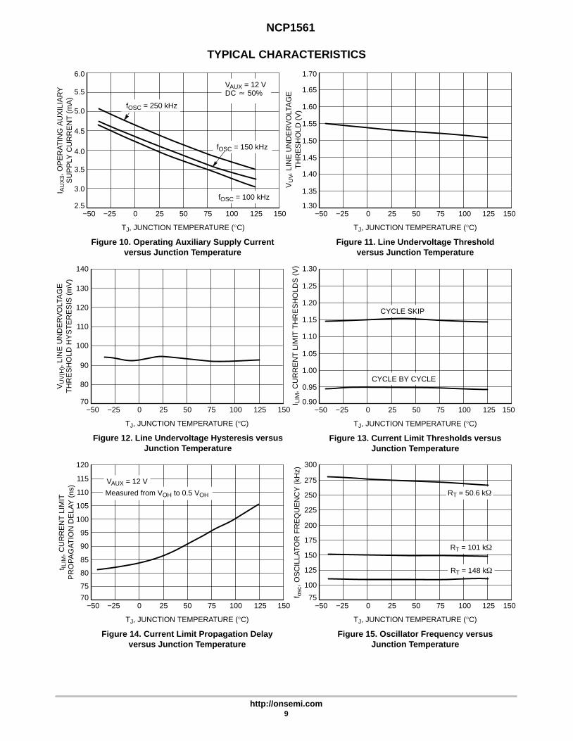
Figure 10. Operating Auxiliary Supply Currentversus Junction Temperature
Figure 11. Line Undervoltage Thresholdversus Junction Temperature
TJ, JUNCTION TEMPERATURE (°C) TJ, JUNCTION TEMPERATURE (°C)
1251007550250−25−502.5
3.0
3.5
4.0
4.5
5.0
5.5
6.0
1251007550250−25−501.30
1.35
1.40
1.45
1.50
1.70
Figure 12. Line Undervoltage Hysteresis versusJunction Temperature
TJ, JUNCTION TEMPERATURE (°C)
150125100250−25−5070
80
90
100
110
120
140
Figure 13. Current Limit Thresholds versusJunction Temperature
TJ, JUNCTION TEMPERATURE (°C)
1251007550250−25−500.90
0.95
1.00
1.05
1.10
1.15
1.25
1.30
I AU
X3,
OP
ER
AT
ING
AU
XIL
IAR
YS
UP
PLY
CU
RR
EN
T (
mA
)
150 150
1.55
1.60
1.65
VU
V, L
INE
UN
DE
RV
OLT
AG
ET
HR
ES
HO
LD (
V)
130
VU
V(H
), LI
NE
UN
DE
RV
OLT
AG
ET
HR
ES
HO
LD H
YS
TE
RE
SIS
(m
V)
150
1.20I L
IM, C
UR
RE
NT
LIM
IT T
HR
ES
HO
LDS
(V
)
7550
fOSC = 250 kHz
CYCLE SKIP
CYCLE BY CYCLE
VAUX = 12 VDC � 50%
fOSC = 150 kHz
fOSC = 100 kHz
Figure 14. Current Limit Propagation Delayversus Junction Temperature
TJ, JUNCTION TEMPERATURE (°C)
1251007550250−25−5070
75
80
85
90
95
115
120
t ILIM
, CU
RR
EN
T L
IMIT
PR
OP
AG
AT
ION
DE
LAY
(ns
)
150
100
105
110
VAUX = 12 V
Measured from VOH to 0.5 VOH
Figure 15. Oscillator Frequency versusJunction Temperature
TJ, JUNCTION TEMPERATURE (°C)
1251007550250−25−5075
100
125
150
175
200
300
150
225
250
275
f osc
, OS
CIL
LAT
OR
FR
EQ
UE
NC
Y (
kHz)
RT = 148 k�
RT = 101 k�
RT = 50.6 k�
NCP1561
http://onsemi.com10
TYPICAL CHARACTERISTICS
Figure 16. Oscillator Frequency versusJunction Temperature
Figure 17. Oscillator Frequency versusTiming Resistor
RT, TIMING RESISTOR (k�)
400300250200150100500
50
100
150
200
300
250
f osc
, OS
CIL
LAT
OR
FR
EQ
UE
NC
Y (
kHz)
350
TJ, JUNCTION TEMPERATURE (°C)
1251007550250−25−50142.5
145.0
147.5
150.0
152.5
155.0
150
157.5
f osc
, OS
CIL
LAT
OR
FR
EQ
UE
NC
Y (
kHz)
RT = 101 k� TJ = 25°CDC � 50%
TJ, JUNCTION TEMPERATURE (°C)
150125100250−25−5020
30
40
50
60
70
100
120
110
RS
NK
/SR
C O
UT
PU
TS
DR
IVE
RE
SIS
TAN
CE
(�
)
50 75
80
90RSRC (VEA = 0 V, VOUT = 10 V)
RSNK (VEA = 3 V, VOUT = 2 V)
VAUX = 12 V
Figure 18. Outputs Drive Resistance versusJunction Temperature
Figure 19. Outputs Rise Time versus LoadCapacitance
CL, LOAD CAPACITANCE (pF)
2001501005000
10
20
30
40
50
60
80
70t o
n, O
UT
PU
TS
RIS
E T
IME
(ns
)
TJ = −40°C
TJ = 25°C
TJ = 125°C
1751257525
Measured from 10% to 90% of VOHVAUX = 12 V
Figure 20. Outputs Fall Time versus LoadCapacitance
CL, LOAD CAPACITANCE (pF)
2001501005000
5
10
15
20
25
35
30
t off,
OU
TP
UT
S F
ALL
TIM
E (
ns)
TJ = −40°C
TJ = 25°CTJ = 125°C
1751257525
Measured from 90% to 10% of VOHVAUX = 12 V
Figure 21. Feedforward Internal Resistanceversus Junction Temperature
150125100750−25−509
10
11
12
13
14
15
19
17
FE
ED
FO
RW
AR
D IN
TE
RN
AL
RE
SIS
TAN
CE
(k�
)
5025
16
18
TJ, JUNCTION TEMPERATURE (°C)
NCP1561
http://onsemi.com11
TYPICAL CHARACTERISTICS
TJ, JUNCTION TEMPERATURE (°C)
1251007550250−25−503.0
3.5
4.0
4.5
5.0
5.5
6.5
7.0
150
6.0
I SS
(C),
SO
FT
−S
TAR
T C
HA
RG
E C
UR
RE
NT
(�A
)
30
35
40
45
50
55
65
70
60
CHARGE
DISCHARGE
52545022515075005
10
20
30
45
DC
MA
X, M
AX
IMU
M D
UT
Y C
YC
LE (
%)
375300
15
25
TJ = −40°C
TJ = 125°C
40
35
VEA = 3.0 VDCMAX PIN = OPEN
TJ, JUNCTION TEMPERATURE (°C)
150125100750−25−5020
25
35
40
45
50
DC
MA
X, M
AX
IMU
M D
UT
Y C
YC
LE (
%)
5025
RP = OPEN, RMDP = OPEN
RP = 0 �, RMDP = OPEN
Vin = 36 VRFF = 432 k�
Figure 22. Maximum Duty Cycle versusFeedforward Current
Figure 23. Maximum Duty Cycle versusJunction Temperature
Figure 24. Soft−Start Charge/DischargeCurrents versus Junction Temperature
ISS
(D) , S
OF
T−
STA
RT
DIS
CH
AR
GE
CU
RR
EN
T (m
A)
IFF, FEEDFORWARD CURRENT (�A)
50
30
Figure 25. VEA Input Resistance versusJunction Temperature
TJ, JUNCTION TEMPERATURE (°C)
150100500−500
10
20
40
50
30
RIN
(VE
A),
VE
A IN
PU
T R
ES
ISTA
NC
E (
k�)
−25 1257525
TJ, JUNCTION TEMPERATURE (°C)
150125100250−25−500.75
0.80
0.85
0.95
1.00
VE
A(L
), P
WM
CO
MP
AR
AT
OR
LO
WE
RIN
PU
T T
HR
ES
HO
LD (
V)
50 75
0.90
Figure 26. PWM Comparator Lower InputThreshold versus Junction Temperature
TJ, JUNCTION TEMPERATURE (°C)
1251007550250−25−504.91
4.93
4.95
4.97
5.01
150
VR
EF,
RE
FE
RE
NC
E V
OLT
AG
E (
V)
IREF = 0 mA
IREF = 6 mA
4.99
Figure 27. Reference Voltage versus JunctionTemperature
RFF = 432 k�Vin = 48 V
NCP1561
http://onsemi.com12
DETAILED OPERATING DESCRIPTION
The NCP1561 is a push−pull PWM controller for use in48 V telecom power converters or 42 V automotivesystems. This controller contains all the features andflexibility required in high density isolated dc−dc modulesand on−board designs for telecom and automotive systems.It can be configured for operation in voltage−mode withfeedforward or current−mode control. The extensive set offeatures included in the NCP1561 facilitates system designand reduces overall system cost and component count byincorporating supervisory functions and componentstraditionally found outside the controller. Features of theNCP1561 include a high voltage startup regulator, fast linefeedforward, a line undervoltage lockout, dual modeovercurrent protection, programmable maximum duty cyclelimit, programmable soft−start and external voltagereference.
Voltage−mode operation with line feedforward providesbetter line regulation without some of the traditionalproblems associated with current−mode control. Thecontroller is configured for voltage−mode operation byrouting the internal Feedforward Ramp output(RAMP_OUT) to the PWM Comparator non−invertinginput (RAMP_IN). The amplitude of the Feedforward Rampvaries inversely proportional to the input voltage. Operationin current−mode control is obtained by routing a signalproportional to the inductor current into the PWMComparator non−inverting input (VEA pin). In either mode,the maximum duty cycle is inversely proportional to the linevoltage, as configured by the DCMAX pin and FF pins.
High Voltage Startup RegulatorThe NCP1561 contains an internal high voltage startup
regulator that eliminates the need for external startupcomponents. In addition, this regulator increases theefficiency of the supply as it uses no power when in thenormal mode of operation, but instead uses power suppliedby an auxiliary winding. The startup regulator consists of aconstant current source that supplies current from the inputline voltage (Vin) to the capacitor on the VAUX pin (CAUX).The startup current is typically 13.0 mA. Once VAUX
reaches approximately 10.3 V, the startup regulator turnsOFF and the outputs are enabled. When VAUX reaches 7.0 V,the outputs are disabled and the startup regulator turns ON.This mode of operation is known as Dynamic Self Supply(DSS).
The startup circuit sources current out of the VAUX pin. Itis recommended to place a diode between CAUX and theauxiliary supply as shown in Figure 28. This will allow theNCP1561 to charge CAUX while preventing the startupregulator from sourcing current into the auxiliary supply.
Figure 28. Recommended VAUX Configuration
ISTART
Disable
CAUX Isupply
VAUX
IAUX
To auxiliary supplyVin
ISTART
Power to the controller while operating in the self−bias orDSS mode is provided by CAUX. Therefore, CAUX must besized such that a VAUX voltage greater than 7.0 V ismaintained while the outputs are enabled and the converterreaches regulation. Also, the VAUX discharge time (from10.3 V to 7.0 V) must be greater than the soft−start chargeperiod to assure the converter turns ON. The startup circuitis rated at a maximum voltage of 150 V. If the deviceoperates in the DSS mode, power dissipation should becontrolled to avoid exceeding the maximum powerdissipation of the controller.
The startup regulator is disabled by biasing VAUX above7.0 V once the outputs are enabled. It can also be disabledby biasing VAUX above VAUX(on) (typically 10.3 V). Thisfeature allows the NCP1561 to operate from an independent12 V (±10%) supply. The independent supply should keepVAUX above VAUX(on). Otherwise the Output Latch will notbe SET and the outputs will remain OFF after a faultcondition is cleared. If operating from an independentsupply, the Vin and VAUX pins should be connected together.
NCP1561
http://onsemi.com13
Line Undervoltage ShutdownThe NCP1561 incorporates a line undervoltage shutdown
(UV) circuit. The undervoltage threshold is approximately1.54 V.
The UV circuit can be biased using an external resistordivider from the input line. The resistor divider must besized to enable the controller once Vin is within the requiredoperating range.
Once the UV condition is removed and VAUX reachesVAUX(on), the controller initiates a soft−start cycle, as shownin Figure 29.
The UV pin can also be used to implement a remoteenable/disable function. Biasing the UV pin below its UVthreshold disables the converter.
If the UV threshold is reached, once in normal operation,the soft−start capacitor is discharged, and the outputs areimmediately disabled as shown in Figure 30. Also, if an UV
condition is detected, the 5.0 V Reference Supply isdisabled.
Figure 30. UV Fault Timing Diagram
OUT2
OUT1
0 V
0 V
0 V
UV Voltage
0 V
UV Fault
VAUX(on)
VAUX(off)
VAUX
VUV
Propagation Delayto Outputs (tUV)
NCP1561
http://onsemi.com14
Feedforward Ramp GeneratorThe NCP1561 incorporates line feedforward (FF) to
compensate for changes in line voltage. A FF Rampproportional to Vin is generated and compared to the errorsignal. If the line voltage changes, the FF Ramp slopechanges accordingly. The duty cycle will be adjustedimmediately instead of waiting for the line voltage changeto propagate around the system and be reflected back onVEA.
A resistor between Vin and the FF pin (RFF) sets thefeedforward current (IFF). The FF Ramp is generated bycharging an internal 10.8 pF capacitor (CFF) with a constantcurrent proportional to IFF. The FF Ramp is finished(capacitor is discharged) once the Oscillator Ramp reaches2.0 V. Please refer to Figure 3 for a functional drawing of theFeedforward Ramp generator.
IFF is usually a few hundred microamps, depending on theoperating frequency and the required duty cycle. If theoperating frequency and maximum duty cycle are known,IFF is calculated using the equation below:
IFF �CFF � VDC(inv) � 125 k�
6.7 k�� ton(max)
where VDC(inv) is the voltage on the inverting input of theMax DC Comparator and ton(max) is the maximum ON time.Figure 22 shows the relationship between IFF and DCMAX.
For example, if a system is designed to operate at anoscillator frequency of 150 kHz, with a 45% maximum dutycycle at 36 V, the DCMAX pin can be grounded and IFF iscalculated as follows:
T � 1f� 1
150 kHz� 6.66 �s
ton(max) � DCMAX � T � 0.45 � 6.66 �s � 3.0 �s
IFF �CFF � VDC(inv) � 125 k�
6.7 k�� ton(max)
�10.8 pF � 1.0 V � 125 k�
6.7 k�� 3.0 �s� 67.2 �A
As the minimum line voltage is 36 V, the requiredfeedforward resistor is calculated using the equation below:
RFF �VinIFF
� 12.0 k� � 36 V67.2 �A
� 12.0 k� � 523 k�
From the above calculations it can be observed that IFF iscontrolled predominantly by the value of RFF, as theresistance seen into the FF pin is only 12 k�. If a tightmaximum duty cycle control over temperature is required,RFF should have a low thermal coefficient. If current−modecontrol is used and the FF Ramp generator is not used formaximum duty cycle control, the FF Ramp generator can bedisabled grounding the FF pin.
NCP1561
http://onsemi.com15
Current LimitThe NCP1561 has two overcurrent protection modes,
cycle by cycle and cycle skip. It allows the NCP1561 tohandle momentary and hard shorts differently for the besttradeoff in system performance and safety. The outputs aredisabled typically 86 ns after a current limit fault is detected.
The cycle by cycle mode terminates the conduction cycle(reducing the duty cycle) if the voltage on the CS pinexceeds 0.95 V. The cycle skip mode is enabled if the voltageon the CS pin reaches 1.15 V. Once a cycle skip fault isdetected, the outputs are disabled, the soft−start and cycleskip capacitors are discharged, and the cycle skip period(TCSKIP) commences.
The cycle skip period is set by an external capacitor(CCSKIP). Once a cycle skip fault is detected, the cycle skipcapacitor is discharged followed by a charge cycle. Thecharge current is 12.3 �A. The cycle skip period ends whenthe voltage on the cycle skip capacitor reaches 2.0 V. If thecycle skip period is known, the cycle skip capacitor iscalculated using the equation below:
CCSKIP �TCSKIP � 12.3 �A
2 VUsing the above equation, a cycle skip period of 11.0 �s
requires a cycle skip capacitor of 68 pF. The differencesbetween the cycle by cycle and cycle skip modes are shownin Figure 31.
Figure 31. Overcurrent Faults Timing Diagram
Cycle Skip Voltage
0 V
0 V
0 V
0 V
0 V
OUT1
OUT2
CS Voltage
NORMALOPERATION RESETFaults
ILIM1
ILIM2
TCSKIP
ILIM
VAUX(off)
VAUX
VAUX(on)
2 V
SOFT−START
Once the cycle skip period is complete and VAUX reachesVAUX(on), a soft−start sequence commences. The possibleminimum OFF time is set by CCSKIP. The actual OFF timeis generally greater than the cycle skip period if operating inDSS because it is the cycle skip period added to the time ittakes VAUX to cycle between VAUX(off) and VAUX(on). Ifoperating from an independent supply, the OFF time is thecycle skip period.
OscillatorThe NCP1561 oscillator frequency is set by a single
external resistor connected between the RT pin and GND.The oscillator is designed to operate up to 250 kHz.
The voltage on the RT pin is laser trim adjusted duringmanufacturing to 1.3 V for an RT of 101 k�. A current setby RT generates an Oscillator Ramp by charging an internal10 pF capacitor as shown in Figure 3. The period ends(capacitor is discharged) once the Oscillator Ramp reaches2.0 V. If RT increases, the current and the Oscillator Rampslope decrease, thus reducing the frequency. If RT decreases,the opposite effect is obtained. Figure 17 shows therelationship between RT and the oscillator frequency.
NCP1561
http://onsemi.com16
Maximum Duty CycleA dedicated internal comparator limits the maximum ON
time by comparing the FF Ramp to VDC(inv) as shown inFigure 3. If the FF Ramp voltage exceeds VDC(inv), theoutput of the Max DC Comparator goes high. This will resetthe Output Latch, thus turning OFF the outputs and limitingthe duty cycle.
Duty cycle is defined as:
DC �tonT
� ton � f
Therefore, the maximum ON time can be set to yield thedesired DC if the operating frequency is known. Themaximum ON time is set by adjusting the FF Ramp to reachVDC(inv) in a time equal to ton(max) as shown in Figure 32.The maximum ON time should be set for the minimum linevoltage. As line voltage increases, the slope of the FF Rampincreases. This reduces the duty cycle below DCMAX, whichis a desirable feature as the duty cycle is inverselyproportional to line voltage.
Figure 32. Maximum ON Time Limit Waveforms
Oscillator Ramp
0 V
0 V
FF Ramp
T
ton(max)
VDC(inv)
2 V
An internal resistor divider from a 2.0 V reference is usedto set VDC(inv). If the DCMAX pin is grounded, VDC(inv) is1.0 V. If the pin is floating, VDC(inv) is 1.4 V. This isequivalent to 71% (36% DC) or 100% (50% DC) of a FFRamp, with a peak voltage of 1.4 V. VDC(inv) can be adjustedto other values by placing an external resistor network on theDCMAX pin. For example, if the minimum line voltage is 36V, RFF is 432 k�, oscillator frequency is 150 kHz and amaximum duty cycle of 45% is required, VDC(inv) iscalculated as follows:
VDC(inv) �IFF � 6.7 k�� ton(max)
CFF � 125 k�
VDC(inv) �81.0 �A � 6.7 k�� 3.0 �s
10.8 pF � 125 k��1.2 V
This can be achieved by connecting a 23.44 k� resistorfrom the DCMAX pin to GND. The maximum duty cyclelimit can be disabled connecting a 100 k� resistor betweenthe DCMAX and VREF pins.
5.0 V ReferenceThe NCP1561 includes a precision 5.0 V reference output.
The reference output is biased directly from VAUX and it cansupply up to 6 mA. Load regulation is 50 mV and lineregulation is 100 mV within the specified operating range.
It is recommended to bypass the reference output with a0.1 �F ceramic capacitor. The reference output is disabledwhen an UV fault is present.
PWM ComparatorIn steady state operation, the PWM Comparator adjusts
the duty cycle by comparing the error signal to the FF Ramp(voltage−mode) or a ramp proportional to the inductorcurrent (current−mode). The error signal is fed into the VEAinput. The FF Ramp or the inductor ramp is fed into theRAMP_IN pin. If operating in voltage−mode, theconnection between the RAMP_OUT and RAMP_IN pinsshould be as close as possible to minimize parasiticinductance. It can be easily routed underneath the package.
The VEA input can be driven directly with an optocouplerand a pull up resistor (REA) from VREF as shown in Figure33. The drive of the control pin is simplified by internallyincorporating a series diode and resistor. The series diodeprovides a 0.7 V offset between the VEA input and the PWMComparator inverting input. The outputs are enabled if theVEA voltage is approximately 0.7 V above the valley voltageof the ramp (Vvalley) in the RAMP_IN pin.
Figure 33. Optocoupler driving VEA input
−
+
−
+
PWMComparator
FF Rampor
Inductor Ramp
FeedbackSignal
RAMP_IN
REA
VREF
VEA
VEA
Vpeak
Vvalley
20 k�
2 k�
0 V12
11
10
The pullup resistor is selected such that in the absence ofthe error signal, the voltage on the VEA pin exceeds the peakamplitude of the ramp in the RAMP_IN pin. Otherwise, theconverter may not be able to reach maximum duty cycle. Ifoperating in voltage−mode, REA is calculated using theequation below:
REA � 22 k�� VREF � 0.7 V
Vvalley � 0.0515�IFFCFF�f
� 1where, CFF is the internal FF capacitor, typically 10.8 pF.
NCP1561
http://onsemi.com17
Soft−StartSoft−start (SS) allows the converter to gradually reach
steady state operation, thus reducing startup stress andsurges on the system. The duty cycle is limited during asoft−start sequence by comparing the Oscillator Ramp to theSS voltage (VSS) by means of the Soft−Start Comparator.
Once faults are removed and VAUX reaches VAUX(on), a6.2 �A current source starts to charge the capacitor on the SSpin. The Soft−Start Comparator controls the duty cyclewhile the SS voltage is below 2.0 V. Once VSS reaches 2.0 V,it exceeds the Oscillator Ramp voltage and the soft−startComparator does not limit the duty cycle. Figure 34 showsthe relationship between the outputs duty cycle and thesoft−start voltage.
Figure 34. Soft Start Timing Diagram
OUT2
OUT1
VSS
OscillatorRamp
If the soft start period is too long, VAUX may discharge to7 V before the converter output is completely in regulationcausing the outputs to be disabled. If the converter output isnot completely discharged when the outputs are re−enabled,the converter will eventually reach regulation exhibiting anon−monotonic startup behavior. But, if the converteroutput is completely discharged when the outputs arere−enabled, the cycle may repeat and the converter will notstart.
In the event of an UV or cycle skip fault, the soft−startcapacitor is discharged. Once the fault is removed, asoft−start cycle commences. The soft−start steady statevoltage is approximately 4.1 V.
Control OutputsThe NCP1561 has two off−phase control outputs, OUT1
and OUT2. Figure 35 shows the relationship between OUT1and OUT2.
Figure 35. Control Outputs Timing Diagram
OUT1
OUT2
Once VAUX reaches VAUX(on), the internal startup circuitis disabled and the One Shot Pulse Generator is enabled. Ifno faults are present, the outputs turn ON. Otherwise, theoutputs remain OFF until the fault is removed and VAUXreaches VAUX(on) again.
The control outputs are biased from VAUX. The outputscan supply up to 10 mA each and their high state voltage isusually 0.2 V below VAUX. Therefore, the auxiliary supplyvoltage should not exceed the maximum input voltage of thedriver stage.
If the control outputs need to drive a large capacitive load,a driver should be used between the NCP1561 and the load.Figures 19 and 20 show the relationship between theoutput’s rise and fall times vs capacitive load.
Thermal ProtectionInternal Thermal Shutdown Circuitry is provided to
protect the integrated circuit in the event the maximumjunction temperature is exceeded. When activated, typicallyat 180�C, the controller is forced into a low power resetstate, discharging the soft−start capacitor and disabling theoutput drivers and the bias regulator. Once the junctiontemperature falls below 163�C, the NCP1561 enters asoft−start mode and it is allowed to resume normaloperation. This feature is provided to prevent catastrophicfailures from accidental device overheating.
Application InformationA dc−dc converter for a 48 V telecom system is designed
and implemented using the NCP1561. The converterdelivers 125 W at 2.5 V and achieves a full load efficiencyof 85%. The system is built using a 4 layer FR4, single sidedboard. The converter footprint is 3.25 in x 3.75 in. Thecomponents location within the board is shown in Figure 36and the complete circuit schematic is shown in Figure 37.The Bill of Material is listed in Table 1. The layout files areavailable. Please contact your sales representative for moreinformation.
NCP1561
http://onsemi.com18
Figure 36. Demo Board Top View
3.75”
3.25”
NCP1561
http://onsemi.com19
Figure 37. NCP1561 Demo Board Circuit Schematic
ON
/OF
F
5V
RE
F5
V R
EF
OU
TB
OU
TB
SE
C_
PW
R
VA
UX
SE
C_
PW
R
R3
6
0
C1
4C
R1
2 BAV70
C3
10
.1
C3
7
R2
7
10k
U4
8
2 31 4567
N/C
IN_
AG
ND
N/C
_1
IN_
BO
UT
_B
VC
CO
UT
_A
R3
16
.2
R3
4
C3
3
C2
21
00
p
CR
4B
AV
70
CR
1B
AV
70
C3
5
TX
4PU
LS
E_
P0
54
4
C6
0.0
1
C2
84
7
TX
3P
UL
SE
_P
05
44
R3
3
R2
95
.49
k
CR
16
R1
1M
R6
CR
9
U6
AL
M2
58
+−
C2
5R
9
C3
6
CR
11
C2
747
C9
R3
5 0
C3
8
Q3
SU
D4
0N
10
−2
5
X7
R2
5
+C
29
R3
2
C1
5
E1
C7
22
C8
0.1
R2
C3
2C
50
.1
U1
NC
P1
56
1
41 3 2 16
15
13
10
89 75
1112
6
14
VF
FV
inR
AM
P_
OU
T
UV
Va
ux
Ou
t1O
ut2
Ve
a
DC
ma
xS
SR
T
CS
Vre
f
RA
MP
_IN
C_
Ski
p
GN
D
L1
R2
31
.43
k
CR
8
R3
7
0
C1
60
.1
R2
82
1.0
k
Q1
C2
10
C4
10
U7
TV
L4
31
A
U3
8
2 31 4567
N/C
IN_
AG
ND
N/C
_1
IN_
BO
UT
_B
VC
CO
UT
_A
SF
H61
5A−
4U
8
C1
2
E2
LM29
31
U2
8
3 417 6
2
5
Vin
GN
DA
DJ
Vo
ut
GN
DG
ND
GN
D
SD
R2
4
T1
PU
LS
E_
PS
82
02
T
CR
10
R8
24
.9k
R5
OP
EN
C1
9
0.1
C4
0O
PE
N
CR
3
Q5
CR
6
R1
3
C1
10
L2
R4
R2
1
R1
72
9.4
k
CR
18
E3
R1
61
.0k
Q6
SU
D4
0N
10
−2
5
E5
X6
C2
00
.1
C1
70
.1
Q2
C1
00
.12
X5
R3
CR
19
OP
EN
CR
2
C2
40
.1
C3
10
C2
1
CR
14
CR
17
U6
BL
M2
58−
R1
8
6.2
R3
0
R2
6C3
9
R1
9
6.2
E4
R7
OP
EN
C1
30
.1
C11
0.2
2
R2
0
R11
6.9
8
R1
2
4T1T
TX
1P
AY
TO
N_
95
57
CR
13
BA
V7
0
CR
15
R2
21
0.0
TX
5
PU
LS
E_
P0
54
4
R1
5
1.0
k
C2
30
.1
Q4
R1
4
R1
0+
C3
0
BA
V7
0
MM
BT
29
07
10
k
110N
02
110N
02 10
00
p
1.0 �H
33
033
0
BA
V7
0
10
00
p
110N
02
110N
02B
AV
70
MMBT2907
10
k
VA
UX
24
9k
10
k
10
0
10
00
p
BA
V7
0
BA
V7
0
BA
V7
0
10
05
23
k
46
.4k
VA
UX
12
4k
BA
V7
0
BA
V7
0
BA
V7
0
75
04
7p
BA
V7
0
BA
V7
0
BA
V7
0
VA
UX
1000
p
10
0p
47
p
75
0
10
k
6.0
4k
10
k
MM
BT
29
07
10
00
p
19
. 6k
27
00
p
20
.5k
18
00
p
10
0p
68
0p
21
.0k
+
C2
6
10
00
p
C3
4
C1
80
.1
2.2 �H
3T1T
OP
EN
2.5
V−+
+ 36 −
72
V−
MC
33
15
2
MC
33
15
20.1
0.1
NCP1561
http://onsemi.com20
Table 1. NCP1561 Demo Board Bill of MaterialQuantity Part Reference Part Value Vendor Comments
1 U2 LM2931CD − ON Semiconductor Voltage Regulator
2 U3, U4 MC33152D − ON Semiconductor MOSFET Driver
1 U6 LM258D − ON Semiconductor Dual OpAmp
1 U7 TVL431ASNT1 − ON Semiconductor Regulator
1 U8 SFH6156−4 − VISHAY Poptocoupler
3 X5−X7 MMBT2907AWT1 − ON Semiconductor PNP transistor
NCP1561
http://onsemi.com21
PACKAGE DIMENSIONS
SO−16D SUFFIX
CASE 751B−05ISSUE J
NOTES:1. DIMENSIONING AND TOLERANCING PER ANSI
Y14.5M, 1982.2. CONTROLLING DIMENSION: MILLIMETER.3. DIMENSIONS A AND B DO NOT INCLUDE
MOLD PROTRUSION.4. MAXIMUM MOLD PROTRUSION 0.15 (0.006)
PER SIDE.5. DIMENSION D DOES NOT INCLUDE DAMBAR
PROTRUSION. ALLOWABLE DAMBARPROTRUSION SHALL BE 0.127 (0.005) TOTALIN EXCESS OF THE D DIMENSION ATMAXIMUM MATERIAL CONDITION.
1 8
16 9
SEATING
PLANE
F
JM
R X 45�
G
8 PLP−B−
−A−
M0.25 (0.010) B S
−T−
D
K
C
16 PL
SBM0.25 (0.010) A ST
DIM MIN MAX MIN MAX
INCHESMILLIMETERS
A 9.80 10.00 0.386 0.393
B 3.80 4.00 0.150 0.157
C 1.35 1.75 0.054 0.068
D 0.35 0.49 0.014 0.019
F 0.40 1.25 0.016 0.049
G 1.27 BSC 0.050 BSC
J 0.19 0.25 0.008 0.009
K 0.10 0.25 0.004 0.009
M 0 7 0 7
P 5.80 6.20 0.229 0.244
R 0.25 0.50 0.010 0.019
� � � �
ON Semiconductor and are registered trademarks of Semiconductor Components Industries, LLC (SCILLC). SCILLC reserves the right to make changes without further noticeto any products herein. SCILLC makes no warranty, representation or guarantee regarding the suitability of its products for any particular purpose, nor does SCILLC assume any liabilityarising out of the application or use of any product or circuit, and specifically disclaims any and all liability, including without limitation special, consequential or incidental damages.“Typical” parameters which may be provided in SCILLC data sheets and/or specifications can and do vary in different applications and actual performance may vary over time. Alloperating parameters, including “Typicals” must be validated for each customer application by customer’s technical experts. SCILLC does not convey any license under its patent rightsnor the rights of others. SCILLC products are not designed, intended, or authorized for use as components in systems intended for surgical implant into the body, or other applicationsintended to support or sustain life, or for any other application in which the failure of the SCILLC product could create a situation where personal injury or death may occur. ShouldBuyer purchase or use SCILLC products for any such unintended or unauthorized application, Buyer shall indemnify and hold SCILLC and its officers, employees, subsidiaries, affiliates,and distributors harmless against all claims, costs, damages, and expenses, and reasonable attorney fees arising out of, directly or indirectly, any claim of personal injury or deathassociated with such unintended or unauthorized use, even if such claim alleges that SCILLC was negligent regarding the design or manufacture of the part. SCILLC is an EqualOpportunity/Affirmative Action Employer. This literature is subject to all applicable copyright laws and is not for resale in any manner.
PUBLICATION ORDERING INFORMATIONN. American Technical Support: 800−282−9855 Toll FreeUSA/Canada
Japan: ON Semiconductor, Japan Customer Focus Center2−9−1 Kamimeguro, Meguro−ku, Tokyo, Japan 153−0051Phone: 81−3−5773−3850
NCP1561/D
LITERATURE FULFILLMENT:Literature Distribution Center for ON SemiconductorP.O. Box 61312, Phoenix, Arizona 85082−1312 USAPhone: 480−829−7710 or 800−344−3860 Toll Free USA/CanadaFax: 480−829−7709 or 800−344−3867 Toll Free USA/CanadaEmail: [email protected]
ON Semiconductor Website: http://onsemi.com
Order Literature: http://www.onsemi.com/litorder
For additional information, please contact yourlocal Sales Representative.