February, 2014 − Rev. 21 Publication Order Number:
NCP6360/D
NCP6360
Mini Buck Converter forRF Power Amplifiers
The NCP6360, a PWM synchronous step−down DC−to−DCconverter, is optimized for supplying RF Power Amplifiers (PAs) usedinto 3G/4G wireless systems (Mobile/ Smart Phones, Phablets,Tablets, ...) powered by single−cell Lithium−Ion batteries. The deviceis able to deliver up to 800 mA. The output voltage is monitorablefrom 0.6 V to 3.4 V by an analog control pin VCON. The analogcontrol allows dynamically optimizing the RF Power Amplifier’sefficiency during a communication while for example in roamingsituation with as a benefit an increased talk time. Also at light load foroptimizing the DC−to−DC converter efficiency, the NCP6360 entersautomatically in a PFM mode and operates in a slower switchingfrequency corresponding to a reduced quiescent current in regards tothe PWM mode for which the device operates at a switching frequencyof 6 MHz. Synchronous rectification offers improved systemefficiency. The NCP6360 is available in a space saving, low profile1.5 x 1.0 mm CSP−6 package.
Features• Input Voltage from 2.7 V to 5.5 V for Battery Powered Applications
• Adjustable Output Voltage (0.6 V to 3.4 V)
• 6 MHz Switching Frequency
• Uses 470 nH Inductor and 4.7 �F Capacitor for Optimized Footprintand Solution Thickness
• PFM /PWM Automatic Mode Change for High Efficiency
See detailed ordering, marking and shipping information onpage 16 of this data sheet.
ORDERING INFORMATION
A = Assembly LocationY = YearW = Work Week� = Pb−Free Package
60AYW�
NCP6360
http://onsemi.com2
Figure 2. Typical Application
3G/4G PAs
RF INAntennaSwitch
Mo
dem
DAC
GPI/O
CouplerRF OUTRF TX
PowerEnvelop
Detection
VBAT
Voltage controlFrom external DAC
Battery or System Supply
10 uF
0.47 uH
4.7 uF
DCDC Out
NCP6360FB
PVIN
SW
PGNDEnabling
ThermalProtection
EN
VCONVout Control
DCDCBuck
1.0 A6.0 MHz
Figure 3. Pin Out (Top View)
1.0 mm
1.5 mm
A2
B2
A1
B1
C1 C2
EN PVIN
VCON SW
FB PGND
NCP6360
http://onsemi.com3
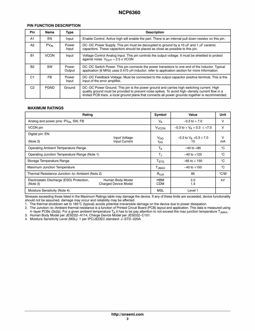
PIN FUNCTION DESCRIPTION
Pin Name Type Description
A1 EN Input Enable Control. Active high will enable the part. There is an internal pull down resistor on this pin.
A2 PVIN PowerInput
DC−DC Power Supply. This pin must be decoupled to ground by a 10 �F and 1 �F ceramiccapacitors. These capacitors should be placed as close as possible to this pin.
B1 VCON Input Voltage Control Analog Input. This pin controls the output voltage. It must be shielded to protectagainst noise. VOUT = 2.5 x VCON
B2 SW PowerOutput
DC−DC Switch Power. This pin connects the power transistors to one end of the inductor. Typicalapplication (6 MHz) uses 0.470 �H inductor; refer to application section for more information.
C1 FB PowerInput
DC−DC Feedback Voltage. Must be connected to the output capacitor positive terminal. This is theinput of the error amplifier.
C2 PGND Ground DC−DC Power Ground. This pin is the power ground and carries high switching current. Highquality ground must be provided to prevent noise spikes. To avoid high−density current flow in alimited PCB track, a local ground plane that connects all power grounds together is recommended.
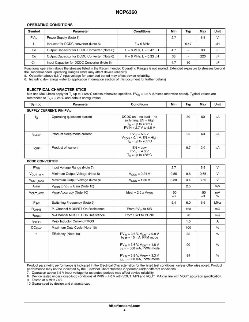
MAXIMUM RATINGS
Rating Symbol Value Unit
Analog and power pins: PVIN, SW, FB VA −0.3 to + 7.0 V
VCON pin VVCON −0.3 to + VA + 0.3 ≤ +7.0 V
Digital pin: EN:Input Voltage
(Note 3) Input CurrentVDGIDG
−0.3 to VA +0.3 ≤ 7.010
VmA
Operating Ambient Temperature Range TA −40 to +85 °C
Operating Junction Temperature Range (Note 1) TJ −40 to +125 °C
Electrostatic Discharge (ESD) Protection, Human Body Model(Note 3) Charged Device Model
HBMCDM
2.01.5
kV
Moisture Sensitivity (Note 4) MSL Level 1
Stresses exceeding those listed in the Maximum Ratings table may damage the device. If any of these limits are exceeded, device functionalityshould not be assumed, damage may occur and reliability may be affected.1. The thermal shutdown set to 165°C (typical) avoids potential irreversible damage on the device due to power dissipation.2. The Junction−to−Ambient thermal resistance is a function of Printed Circuit Board (PCB) layout and application. This data is measured using
4−layer PCBs (2s2p). For a given ambient temperature TA it has to be pay attention to not exceed the max junction temperature TJMAX.3. Human Body Model per JESD22−A114, Charge Device Model per JESD22−C101.4. Moisture Sensitivity Level (MSL): 1 per IPC/JEDEC standard: J−STD−020A.
NCP6360
http://onsemi.com4
OPERATING CONDITIONS
Symbol Parameter Conditions Min Typ Max Unit
PVIN Power Supply (Note 5) 2.7 5.5 V
L Inductor for DCDC converter (Note 6) F = 6 MHz 0.47 �H
Co Output Capacitor for DCDC Converter (Note 6) F = 6 MHz, L = 0.47 �H 4.7 − 33 �F
Co Output Capacitor for DCDC Converter (Note 6) F = 6 MHz, L = 0.33 �H 33 − 220 �F
Functional operation above the stresses listed in the Recommended Operating Ranges is not implied. Extended exposure to stresses beyondthe Recommended Operating Ranges limits may affect device reliability.5. Operation above 5.5 V input voltage for extended period may affect device reliability.6. Including de−ratings (refer to application information section of this document for further details)
ELECTRICAL CHARACTERISTICSMin and Max Limits apply for TJ up to +125°C unless otherwise specified. PVIN = 3.6 V (Unless otherwise noted). Typical values arereferenced to TA = + 25°C and default configuration
Symbol Parameter Conditions Min Typ Max Unit
SUPPLY CURRENT: PIN PVIN
IQ Operating quiescent current DCDC on – no load – noswitching, EN = High
TA = up to +85°CPVIN = 2.7 V to 5.5 V
30 50 �A
ISLEEP Product sleep mode current PVIN = 5.5 VVCON < 0.1 V, EN = High
TA = up to +85°C
25 60 �A
IOFF Product off current EN = LowPVIN = 4.6 V
TA = up to +85°C
0.7 2.0 �A
DCDC CONVERTER
PVIN Input Voltage Range (Note 7) 2.7 5.5 V
VOUT_MIN Minimum Output Voltage (Note 8) VCON = 0.24 V 0.55 0.6 0.65 V
VOUT_MAX Maximum Output Voltage (Note 8) VCON = 1.36 V 3.30 3.4 3.50 V
Product parametric performance is indicated in the Electrical Characteristics for the listed test conditions, unless otherwise noted. Productperformance may not be indicated by the Electrical Characteristics if operated under different conditions.7. Operation above 5.5 V input voltage for extended periods may affect device reliability.8. Device tested under closed-loop conditions at PVIN = 4.0 V with VOUT_MIN and VOUT_MAX in line with VOUT accuracy specification.9. Tested at 6 MHz / 48.10.Guaranteed by design and characterized.
NCP6360
http://onsemi.com5
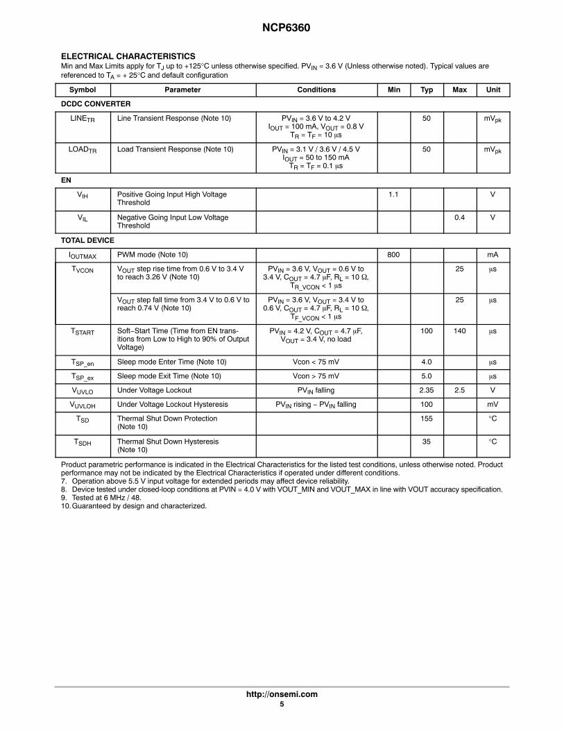
ELECTRICAL CHARACTERISTICSMin and Max Limits apply for TJ up to +125°C unless otherwise specified. PVIN = 3.6 V (Unless otherwise noted). Typical values arereferenced to TA = + 25°C and default configuration
Symbol UnitMaxTypMinConditionsParameter
DCDC CONVERTER
LINETR Line Transient Response (Note 10) PVIN = 3.6 V to 4.2 VIOUT = 100 mA, VOUT = 0.8 V
TR = TF = 10 �s
50 mVpk
LOADTR Load Transient Response (Note 10) PVIN = 3.1 V / 3.6 V / 4.5 VIOUT = 50 to 150 mA
TR = TF = 0.1 �s
50 mVpk
EN
VIH Positive Going Input High VoltageThreshold
1.1 V
VIL Negative Going Input Low VoltageThreshold
0.4 V
TOTAL DEVICE
IOUTMAX PWM mode (Note 10) 800 mA
TVCON VOUT step rise time from 0.6 V to 3.4 Vto reach 3.26 V (Note 10)
VUVLO Under Voltage Lockout PVIN falling 2.35 2.5 V
VUVLOH Under Voltage Lockout Hysteresis PVIN rising − PVIN falling 100 mV
TSD Thermal Shut Down Protection(Note 10)
155 °C
TSDH Thermal Shut Down Hysteresis(Note 10)
35 °C
Product parametric performance is indicated in the Electrical Characteristics for the listed test conditions, unless otherwise noted. Productperformance may not be indicated by the Electrical Characteristics if operated under different conditions.7. Operation above 5.5 V input voltage for extended periods may affect device reliability.8. Device tested under closed-loop conditions at PVIN = 4.0 V with VOUT_MIN and VOUT_MAX in line with VOUT accuracy specification.9. Tested at 6 MHz / 48.10.Guaranteed by design and characterized.
NCP6360
http://onsemi.com6
TYPICAL OPERATING CHARACTERISTICSPVIN = EN = 3.6 V, L = 0.47 �H, COUT = 4.7 �F, CIN = 10 �F, Fsw = 6 MHz, TA = 25°C (unless otherwise noted)
TBD
Figure 4. Shutdown Current vs Input Voltage(EN = Low, VCON = 0 V)
Figure 5. Shutdown Current vs Temperature(EN = Low, VCON = 0 V)
Figure 6. Sleep Mode Current vs Input Voltage(EN = High, VCON = 0 V, VOUT = 0 V)
Figure 7. Sleep Mode Current vs. Temperature(EN = High, VCON = 0 V, VOUT = 0 V)
Figure 8. Quiescent Current vs Input Voltage(EN = High, VCON = 0.8 V, VOUT = 2 V, no load)
Figure 9. Quiescent Current vs Temperature (TA)(EN = High, VCON = 0.8 V, VOUT = 2 V, no load)
NCP6360
http://onsemi.com7
TYPICAL OPERATING CHARACTERISTICSPVIN = EN = 3.6 V, L = 0.47 �H, COUT = 4.7 �F, CIN = 10 �F, Fsw = 6 MHz, TA = 25°C (unless otherwise noted)
Figure 10. VOUT Accuracy vs. OutputCurrent vs. PVIN @ 25�C, VOUT = 0.8 V
Figure 11. VOUT Accuracy vs. Output Current vs.Temperature PVIN = 3.6 V, VOUT = 0.8 V
Figure 12. VOUT Accuracy vs. OutputCurrent vs. PVIN @ 25�C, VOUT = 1.8 V
Figure 13. VOUT Accuracy vs. Output Currentvs. Temperature PVIN = 3.6 V, VOUT = 1.8 V
Figure 14. VOUT Accuracy vs. OutputCurrent vs. PVIN @ 25�C, VOUT = 3.3 V
Figure 15. VOUT Accuracy vs. Output Currentvs. Temperature PVIN = 4.2 V, VOUT = 3.3 V
NCP6360
http://onsemi.com8
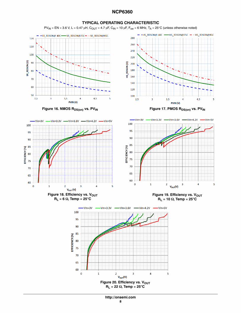
TYPICAL OPERATING CHARACTERISTICPVIN = EN = 3.6 V, L = 0.47 �H, COUT = 4.7 �F, CIN = 10 �F, Fsw = 6 MHz, TA = 25°C (unless otherwise noted)
Figure 16. NMOS RDS(on) vs. PVIN Figure 17. PMOS RDS(on) vs. PVIN
General DescriptionThe NCP6360 is a voltage−mode standalone synchronous
step−down DC−to−DC converter designed to supply RFPower Amplifiers (PAs) used into 3G/4G wireless systems(Mobile/ Smart Phones, Phablets, Tablets, ...) powered bysingle−cell Lithium−Ion batteries. The IC can deliver up to800 mA when operating in PWM mode.
The buck converter output voltage ranging from 0.6 V to3.4 V can be monitored by the system’s PA output RF powerthrough the control pin VCON. The control voltage range isfrom 0.24 V to 1.36 V and Vout is equal to 2.5 times thiscontrol voltage. VCON allows the PA to have its efficiencydynamically optimized during communication calls in thecase for example of roaming situation involving a constantadjustment of the PA output power. The value−added benefitis an increase of the absolute talk time.
Synchronous rectification and automatic PFM/PWMoperating mode transitions improve overall solutionefficiency. The device operates at 6 MHz switchingfrequency.
Buck DC−to−DC Converter OperatingThe converter is a synchronous rectifier type with both
high side and low side integrated switches. Neither externaltransistor nor diodes are required for NCP6360 operation.Feedback and compensation network are also fullyintegrated. The device can operate in four different modes:shutdown mode (EN = Low, device off), Sleep Mode whenVCON below about 0.1 V, PFM mode for efficiencyoptimization purpose when operating at light load and PWMmode when operating in medium and high loads. Thetransitions between PWM and PFM modes occurautomatically.
Shutdown ModeThe NCP6360 enters shutdown mode when setting the EN
pin Low (below 0.4 V) or when PVIN drops below itsUVLO threshold value (2.35 V typical). In shutdown mode,the internal reference, oscillator and most of the controlcircuitries are turned off. The typical current consumption is0.7 �A. Applying a voltage above 1.1 V to EN pin willenable the device for normal operation. A soft−startsequence is run when activating EN high. EN pin should beactivated after the input voltage is applied.
PWM (Pulse Width Modulation) Operating ModeIn medium and high load conditions, the NCP6360
operates in PWM mode from a fixed clock (6 MHz) andadapts its duty cycle to regulate the desired output voltage.In this mode, the inductor current is in CCM (ContinuousCurrent Mode) and the voltage is regulated by PWM. Theinternal N−MOSFET switch operates as synchronousrectifier and is driven complementary to the P−MOSFETswitch. In CCM, the lower switch (N−MOSFET) in a
synchronous converter provides a lower voltage drop thanthe diode in an asynchronous converter, which provides lessloss and higher efficiency.
PFM (Pulse Frequency Modulation) Operating ModeIn order to save power and improve efficiency at low loads
the NCP6360 operates in PFM mode as the inductor dropsinto DCM (Discontinuous Current Mode). The upper FETon time is kept constant and the switching frequency isvariable. Output voltage is regulated by varying theswitching frequency which becomes proportional to loadingcurrent. As it does in PWM mode, the internal N−MOSFEToperates as synchronous rectifier after each P−MOSFETon−pulse. When load increases and current in inductorbecomes continuous again, the controller automaticallyturns back to PWM mode.
Sleep ModeThe NCP6360 device enters the sleep mode in about 4�s
when the control voltage VCON goes below typically70 mV. Vout is extremely low, close to 0 V and in a state outof regulation. In this Vout condition the Sleep mode enablesa low current state (40 �A typical range). The buckconverter exits the sleep mode and returns in a regulationstate when VCON goes above 110 mV after typically 5 �s.
Inductor Peak Current limitationsDuring normal operation, peak current limitation will
monitor and limit the current through the inductor. Thiscurrent limitation is particularly useful when size and/orheight constrain inductor power. The High Side Switch(HSS) peak current limitation is typically 1.5 A, while theLow Side Switch (LSS) has a peak current up to 0.8 A. TheHSS peak current contributes to limit the current during softstart sequence in high load conditions.
Under−voltage Lockout (UVLO)NCP6360 core does not operate for voltages below the
Under Voltage lock Out (UVLO) level. Below UVLOthreshold (typical 2.35 V), all internal circuitry (both analogand digital) is held in reset. NCP6360 operation is notguaranteed down to VUVLO when battery voltage isdropping off. To avoid erratic on / off behavior,a typical100 mV hysteresis is implemented. Restart is guaranteed at2.6 V when VBAT voltage is recovering or rising.
Power−Up / Power−Down SequencingThe EN pin controls NCP6360 start up. EN pin Low to
High transition starts the power up sequencer which iscombined with a soft start consisting to limit the inrushcurrent at 800 mA while the output voltage is establishing.If EN is made low, the DC to DC converter is turned off anddevice enters shutdown mode.
A built−in pull−down resistor disables the device whenthis pin is left unconnected or not driven.
NCP6360
http://onsemi.com13
Wake Up Time ~ TBD
PVIN
EN
VOUT
POR
Rising UVLO < 2.6 V
Soft Start 800mA
HSS IpeakIOUT
Figure 37. Power−Up Sequence
In order to power up the circuit, the input voltage PVINhas to rise above the UVLO threshold (Rising UVLO). Thistriggers the internal core circuitry power up which is the“Wake Up Time” (including “Bias Time”).
This delay is internal and cannot be bypassed.The power down sequence is triggered by setting Low the
EN pin. The output voltage goes down to 0 V.
Thermal Shutdown Feature (TSD)The thermal capability of IC can be exceeded due to step
down converter output stage power level. A thermalprotection circuitry is therefore implemented to prevent the
IC from damage. This protection circuitry is only activatedwhen the core is in active mode (output voltage is turned on).During thermal shut down, output voltage is turned off andthe device enters sleep mode.
Thermal shut down threshold is set at 155°C (typical)when the die temperature increases and, in order to avoiderratic on / off behavior, a 35°C hysteresis is implemented.So, after a typical 155°C thermal shut down, the NCP6360will return to normal operation when the die temperaturecools to 120°C. This normal operation depends on the inputconditions and configuration at the time the device recovers.
NCP6360
http://onsemi.com14
APPLICATION INFORMATION
Figure 38. Typical Application Schematic
3G/4G PAs
RF INAntennaSwitch
Mo
dem
DAC
GPI/O
CouplerRF OUTRF TX
PowerEnvelop
Detection
VBAT
Voltage controlFrom external DAC
Battery or System Supply
10 uF
0.47 uH
4.7 uF
DCDC Out
NCP6360FB
PVIN
SW
PGNDEnabling
ThermalProtection
EN
VCONVout Control
DCDCBuck
1.0 A6.0 MHz
Output Filter Design ConsiderationsThe output filter introduces a double pole in the system at
a frequency of:
fLC �1
2 � � � L � C�(eq. 1)
The NCP6360 internal compensation network isoptimized for a typical output filter comprising a 470 nHinductor and one 4.7 �F capacitor as described in the basicapplication schematic Figure 38.
Inductor SelectionThe inductance of the inductor is determined by given
peak−to−peak ripple current ILPP of approximately 20% to
50% of the maximum output current IOUTMAX for atrade−off between transient response and output ripple. Theselected inductor must have high enough saturation currentrating to be higher than the maximum peak current that is:
ILMAX � IOUTMAX �ILPP
2(eq. 2)
The inductor also needs to have high enough currentrating based on temperature rise concern. Low DCR is goodfor efficiency improvement and temperature rise reduction.Tables 1 shows recommended inductor references.
Table 1. RECOMMENDED INDUCTORS WHEN OPERATING AT 6 MHz
Supplier Part# Value (�H)Size (L x l x T)
(mm)DC Rated Current
(A)DCR Max @ 25�C
(m�)
TDK TFM201610A−R47M−T00 0.47 20x16x1 3.5 46
TDK TFM201210A−R47M−T00 0.47 20x12x1 2.5 65
Toko DFE201610R−R47M−T00 0.47 20x16x1 3.8 48
Toko DFE201610A−R47M−T00 0.47 20x16x1 3.7 58
NCP6360
http://onsemi.com15
Output Capacitor SelectionThe output capacitor selection is determined by output
voltage ripple and load transient response requirement. Forhigh transient load performance high output capacitor valuemust be used. For a given peak−to−peak ripple current ILPP
in the inductor of the output filter, the output voltage rippleacross the output capacitor is the sum of three componentsas below.
VOUTPP � VOUTPP(C) � VOUTPP(ESR) � VOUTPP(ESL)
(eq. 3)
Where VOUTPP(C) is the ripple component coming froman equivalent total capacitance of the output capacitors,VOUTPP(ESR) is a ripple component from an equivalent ESRof the output capacitors, and VOUTPP(ESL) is a ripplecomponent from an equivalent ESL of the output capacitors.In PWM operation mode, the three ripple components canbe obtained by
VOUTPP(C) �IL_PP
8 � C � fSW
(eq. 4)
VOUTPP(ESR) � ILPP � ESR (eq. 5)
VOUT_PP(ESL) �ESL
ESL � L� VIN (eq. 6)
And the peak−to−peak ripple current is:
ILPP ��PVIN � VOUT
� � VOUT
PVIN � FSW � L(eq. 7)
In applications with all ceramic output capacitors, themain ripple component of the output ripple is VOUTPP(C).So that the minimum output capacitance can be calculatedregarding to a given output ripple requirement VOUTPP inPWM operation mode.
CMIN �ILPP
8 � VOUTPP � fSW
(eq. 8)
Input Capacitor SelectionOne of the input capacitor selection guides is the input
voltage ripple requirement. To minimize the input voltage
ripple and get better decoupling in the input power supplyrail, ceramic capacitor is recommended due to low ESR andESL. The minimum input capacitance regarding the inputripple voltage VINPP is
CINMIN �IOUTMAX � �D � D2�
VINPP � fSW
(eq. 9)
Where
D �VOUT
VIN
(eq. 10)
In addition the input capacitor needs to be able to absorbthe input current, which has a RMS value of:
IINRMS � IOUTMAX � D � D2� (eq. 11)
The input capacitor needs also to be sufficient to protectthe device from over voltage spike and a minimum of 4.7 �Fcapacitor is required. The input capacitor should be locatedas close as possible to the IC. PGND is connected to theground terminal of the input cap which then connects to theground plane. The PVIN is connected to the VBAT terminalof the input capacitor which then connects to the VBATplane.
Layout and PCB Design RecommendationsGood PCB layout helps high power dissipation from a
small package with reduced temperature rise. Thermallayout guidelines are:• A four or more layers PCB board with solid ground
planes is preferred for better heat dissipation.• More free vias are welcome to be around IC to connect
the inner ground layers to reduce thermal impedance.• Use large area copper especially in top layer to help
thermal conduction and radiation.• Use two layers for the high current paths (PVIN,
PGND, SW) in order to split current in two differentpaths and limit PCB copper self heating.
(See demo board example Figure 40)
NCP6360
http://onsemi.com16
Figure 39. Layout Minimum Recommended Occupied Space Using 0402 Capacitors and 0805(2.0 x1.2 x1 mm) Inductor
04021.5 x 0.9 m
m
3.60 mm
2.80 mm
S < 10.1 mm�
0402 TF
M201210
2.0 x 1.2 mmPVIN
SW
EN
VCON
FB PGND
1.5 x 0.9 mm
Input capacitor placed as close as possible to the IC.• PVIN directly connected to Cin input capacitor, and
then connected to the Vin plane. Local mini planes usedon the top layer (green) and layer just below top layerwith laser vias.
• PGND directly connected to Cin input capacitor, andthen connected to the GND plane: Local mini planes
used on the top layer (green) and layer just below toplayer with laser vias.
• SW connected to the Lout inductor with local miniplanes used on the top layer (green) and layer justbelow top layer with laser vias.
Figure 40. Example of PCB Implementation (PCB case with 0805 (2.0x1.2 mm) Capacitors and 2016 (2.0 x 1.6 x 1 mm) Inductors
ORDERING INFORMATION
Device Package Shipping†
NCP6360FCCT2G WLCSP6(Pb−Free)
3000 / Tape & Reel
†For information on tape and reel specifications, including part orientation and tape sizes, please refer to our Tape and Reel PackagingSpecifications Brochure, BRD8011/D.
NCP6360
http://onsemi.com17
PACKAGE DIMENSIONS
WLCSP6, 1.00x1.50CASE 567AN
ISSUE A
SEATINGPLANE
0.05 C
NOTES:1. DIMENSIONING AND TOLERANCING PER
ASME Y14.5M, 1994.2. CONTROLLING DIMENSION: MILLIMETERS.3. COPLANARITY APPLIES TO SPHERICAL
CROWNS OF SOLDER BALLS.
2X
DIMA
MIN MAX0.54
MILLIMETERS
A1
D 1.00 BSCE
b 0.315 0.335
e 0.50 BSC
0.63
ÈÈÈÈ
D
E
A BPIN A1
REFERENCE
e
A0.05 BC
0.03 C
0.05 C
6X b
1 2 3
C
B
A
0.05 C
A
A1
A2
C
0.21 0.26
1.50 BSC
0.500.256X
DIMENSIONS: MILLIMETERS
*For additional information on our Pb−Free strategy and solderingdetails, please download the ON Semiconductor Soldering andMounting Techniques Reference Manual, SOLDERRM/D.
SOLDERING FOOTPRINT*
0.05 C2XTOP VIEW
SIDE VIEW
BOTTOM VIEW
NOTE 3
e
A2 0.36 REF
RECOMMENDED
A1PACKAGEOUTLINE
PITCH
0.50PITCH
A3
DETAIL A
DIE COAT
DETAIL A
A2
A3 0.02 REF
ON Semiconductor and are registered trademarks of Semiconductor Components Industries, LLC (SCILLC). SCILLC owns the rights to a number of patents, trademarks,copyrights, trade secrets, and other intellectual property. A listing of SCILLC’s product/patent coverage may be accessed at www.onsemi.com/site/pdf/Patent−Marking.pdf. SCILLCreserves the right to make changes without further notice to any products herein. SCILLC makes no warranty, representation or guarantee regarding the suitability of its products for anyparticular purpose, nor does SCILLC assume any liability arising out of the application or use of any product or circuit, and specifically disclaims any and all liability, including withoutlimitation special, consequential or incidental damages. “Typical” parameters which may be provided in SCILLC data sheets and/or specifications can and do vary in different applicationsand actual performance may vary over time. All operating parameters, including “Typicals” must be validated for each customer application by customer’s technical experts. SCILLCdoes not convey any license under its patent rights nor the rights of others. SCILLC products are not designed, intended, or authorized for use as components in systems intended forsurgical implant into the body, or other applications intended to support or sustain life, or for any other application in which the failure of the SCILLC product could create a situation wherepersonal injury or death may occur. Should Buyer purchase or use SCILLC products for any such unintended or unauthorized application, Buyer shall indemnify and hold SCILLC andits officers, employees, subsidiaries, affiliates, and distributors harmless against all claims, costs, damages, and expenses, and reasonable attorney fees arising out of, directly or indirectly,any claim of personal injury or death associated with such unintended or unauthorized use, even if such claim alleges that SCILLC was negligent regarding the design or manufactureof the part. SCILLC is an Equal Opportunity/Affirmative Action Employer. This literature is subject to all applicable copyright laws and is not for resale in any manner.
PUBLICATION ORDERING INFORMATIONN. American Technical Support: 800−282−9855 Toll FreeUSA/Canada
Europe, Middle East and Africa Technical Support:Phone: 421 33 790 2910
Japan Customer Focus CenterPhone: 81−3−5817−1050
NCP6360/D
LITERATURE FULFILLMENT:Literature Distribution Center for ON SemiconductorP.O. Box 5163, Denver, Colorado 80217 USAPhone: 303−675−2175 or 800−344−3860 Toll Free USA/CanadaFax: 303−675−2176 or 800−344−3867 Toll Free USA/CanadaEmail: [email protected]
ON Semiconductor Website: www.onsemi.com
Order Literature: http://www.onsemi.com/orderlit
For additional information, please contact your localSales Representative