59
NCR 5380 SCSI Interface Chip Design Manual Microelectronics Division, Colorado Springs
NCR 5380 SCSI
Interface Chip
Design Manual
Microelectronics Division, Colorado Springs
Copyright © 1985, by NCR Corporation Dayton, Ohio
All Rights Reserved Printed in U.S.A.
This document contains the latest information available at the time of publication. However, NCR
reserves the right to modify the contents of this material at any time. Also, all features, functions and
operations described herein may not be marketed by NCR in all parts of the world. Therefore, before
using this document, consult your NCR representative or NCR office for the information that is applic
able and current.
SECTION 1. 2. 3. 4.
5. 6.
7. 8.
TABLE OF CONTENTS
PAGE General Description ............................................................. 3 SCSI Background .............................................................. 4 Block Diagram ................................................................. 5 Pin Description .................................................................. . 4.1 Microprocessor Interface Signals .......................................... 6 4.2 SCSI Interface Signals ................................................... 8 Electrical Characteristics ........................................................ 9 Internal Registers ................................................................ . 6.0 General ................................................................. 10 6.1 Data Registers .......................................................... 10
6.1.1 Current SCSI Data Register ............................................. 10 6.1.2 Output Data Register ................................................... 10 6.1.3 Input Data Register ..................................................... 11
6.2 Initiator Command Register ............................................... 11 6.3 Mode Register .......................................................... 13 6.4 Target Command Register ............................................... 14 6.5 Current SCSI Bus Status Register ......................................... 15 6.6 Select Enable Register ................................................... 15 6.7 Bus and Status Register ................................................. 15 6.8 DMA Registers .......................................................... 16
6.8.1 Start DMA Send ....................................................... 16 6.8.2 Start DMA Target Receive .............................................. 17 6.8.3 Start DMA Initiator Receive .............................................. 17
6.9 Reset Parity/ Interrupt .................................................... 17 On-Chip SCSI Hardware Support ................................................. 18 Interrupts ....................................................................... . 8.1 Selection/ Reselection ................................................... 19 8.2 End of Process (EOP) Interrupt ........................................... 20 8.3 SCSI Bus Reset ........................................................ 21 8.4 Parity Error ............................................................. 21 8.5 Bus Phase Mismatch .................................................... 22 8.6 Loss of BSY ............................................................ 22
9. Reset Conditions ............................................................... 23 9.1 Hardware Chip Reset .................................................... 23 9.2 SCSI Bus Reset Received ............................................... 23 9.3 SCSI Bus Reset Issued .................................................. 23
10. Data Transfers ................................................................. 24 10.1 Programmed 110 Transfers ............................................... 24 10.2 Normal DMA Mode ...................................................... 24 10.3 Block Mode DMA ....................................................... 24 10.4 Pseudo DMA Mode ...................................................... 25 10.5 Halting a DMA Operation ................................................. 25
10.5.1 Using the EOP Signal .................................................. 25 10.5.2 Bus Phase Mismatch Interrupt ........................................... 25 10.5.3 Resetting the DMA MODE Bit ........................................... 25
11. External Timing Diagrams 11.1 CPU Write .............................................................. 26 11.2 CPU Read ............................................................. 26 11.3 DMA Write (Non-block Mode) Target Send ................................. 27 11.4 DMA Write (Non-block Mode) Initiator Send ................................ 28 11.5 DMA Read (Non-block Mode) Target Receive .............................. 29 11.6 DMA Read (Non-block Mode) Initiator Receive ............................. 30 11.7 DMA Write (Block Mode) Target Send ..................................... 31 11.8 DMA Read (Block Mode) Target Receive .................................. 32 11.9 Reset .................................................................. 33 11 .10 Arbitration .............................................................. 33
APPENDICES
A 1. NCR 5380 vs. NCR 5385/86 .................................................... 34 A2. Flowchartsl Software ............................................................ 35 A3. 65C02 Interface Diagram ........................................................ 50 A4. NCR 5381 Differential Pair Option ................................................ 51 A5. SCSII Plus ..................................................................... 54 A6. Register Reference Chart ....................................................... 56
2
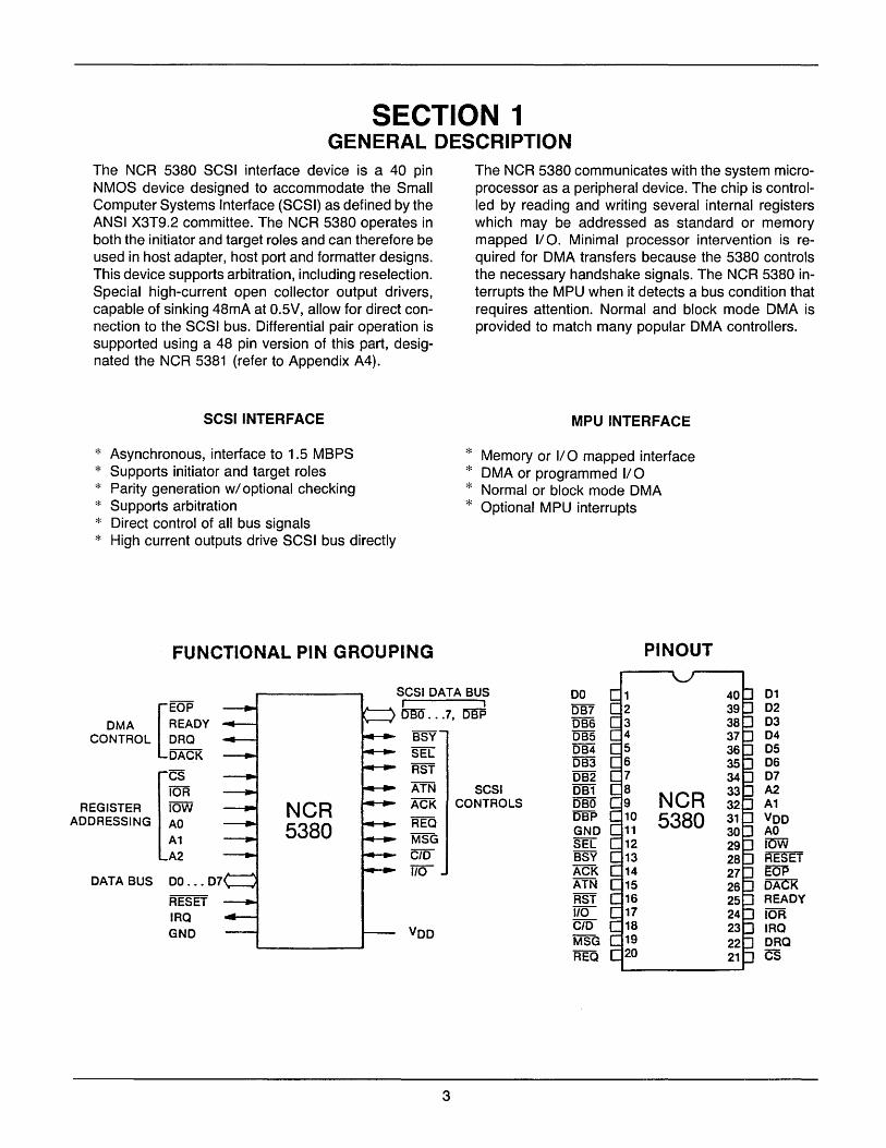
SECTION 1 GENERAL DESCRIPTION
The NCR 5380 SCSI interface device is a 40 pin NMOS device designed to accommodate the Small Computer Systems Interface (SCSI) as defined by the ANSI X3T9.2 committee. The NCR 5380 operates in both the initiator and target roles and can therefore be used in host adapter, host port and formatter designs. This device supports arbitration, including reselection. Special high-current open collector output drivers, capable of sinking 48mA at 0.5V, allow for direct connection to the SCSI bus. Differential pair operation is supported using a 48 pin version of this part, designated the NCR 5381 (refer to Appendix A4).
SCSI INTERFACE
* Asynchronous, interface to 1.5 MBPS * Supports initiator and target roles * Parity generation wi optional checking * Supports arbitration * Direct control of all bus signals * High current outputs drive SCSI bus directly
FUNCTIONAL PIN GROUPING
The NCR 5380 communicates with the system microprocessor as a peripheral device. The chip is controlled by reading and writing several internal registers which may be addressed as standard or memory mapped 1/0. Minimal processor intervention is required for DMA transfers because the 5380 controls the necessary handshake signals. The NCR 5380 interrupts the MPU when it detects a bus condition that requires attention. Normal and block mode DMA is provided to match many popular DMA controllers.
MPUINTERFACE
* Memory or 110 mapped interface * DMA or programmed 1/0 * Normal or block mode DMA * Optional MPU interrupts
PINOUT
SCSI DATA BUS DO 01
[EOP i I DB7 02 DMA READY
OSO ... 7, DBP OB6 03
CONTROL ORO BSY DB5 04 SEL OB4 05 OACK OB3 06
CS RST OB2 07 lOR ATN SCSI OB1
NCR A2
REGISTER lOW NCR ACK CONTROLS DBO A1 ADDRESSING REO DBP 5380 VOO AD 5380 GND AD
A1 MSG SEL lOW A2 C/O BSY RESET
110 ACK EOP DATA BUS ATN DACR
RESET RST READY IRO 110 lOR GNO VOD C/O IRa
MSG ORO REO CS
3
SECTION 2 SCSI BACKGROUND
SCSI (Small Computer Systems Interface) has evolved from the SASI (Shugart Associates Systems Interface) disk controller interface standard developed by Shugart Associates in the late 1970's. NCR and Shugart jointly approached the ANSC X3T9.3 subcommittee in December of 1981 and proposed that a committee be formed to develop an intelligent interface standard based on SASI. The ANSC X3T9.3 subcommittee divided into two groups so that SASI could be pursued. In February of 1982, NCR and Shugart Associates presented SASI as a working document. It was agreed that a separate group should develop the standard and the ANSC X3T9.2 subcommittee was established. This group met in April of that year and formally changed the name to the Small Computer Systems Interface (SCSI).
The proposed standard has since been forwarded from the subcommittee and is becoming a major industry standard. It is expected that other standards organizations such as ECMA (European Computer Manufactures Association) and ISO (International Standards Organization) will adopt the proposed standard as well.
NCR Microelectronics announced the NCR 5385, the first SCSI protocol controller, in April of 1983. This product family includes the NCR 5386 and the soon-to-be-announced NCR 5386S. The NCR 5380 and 5381 were designed to compliment this initial offering. Differences between the product families are described in Appendix A 1.
This design manual is not an SCSI specification and assumes some prior knowledge of the SCSI proposed standard. Copies of the proposed standard may be obtained, with pre-payment of $20, from:
X3 Secretariat, Computer and Business Equipment Manufacturers Association 311 First Street, NW, Suite 500 Washington, D.C. 20001
Please include a self-addressed mailing label.
4
Other documents which may be useful are:
• NCR 5385 SCSI Protocol Controller Data Sheet (MC-704)
• NCR 5385 SCSI Protocol Controller User's Guide (MC-903)
• SCSI Engineering Notebook
These documents may be obtained by contacting your local NCR Microelectronics sales representative or by writing/ calling:
NCR Microelectronics Logic Products Marketing 1635 Aeroplaza Drive Colorado Springs, CO 80916 PH# 1-800-525-2252
EOP OACK CPU
INTERFACE
Reset parity
EOP,ORQ
or interrupt register
DMA control
(Start OMA send, start OMA target
receive, start OMA initiator
receive)
Parity checking
Arbitration logic
CS, lOR,
lOW Ao, AI, A2
r-
v Address decoding
logic
I --I
I
--1_
Bus phase comparison
1/0, C/O,
MSG,REQ
enable register
Identification comparison
Input data register
Current SCSI data
register
Data output register
Parity generator
------------1 High-current open-collector output drivers I
I --t--SCSI BUS INTERFACE
- -, I I
_J
SECTION 4 PIN DESCRIPTION
4.1 Microprocessor Interface Signals
Pin Name Pin #
AO,A1,A2 30, 32, 33
21
26
ORO 22
00 ... 07 1,40 ... 34
27
24
Description
INPUTS These signals are used with CS, lOR or lOW to address all internal registers.
INPUT Chip Select enables a read or write of the internal register selected by AO, A 1 and A2. CS is an active low signal.
INPUT DMA Acknowledge resets DRO and selects the data register for input or output data transfers. DACK is an active low signal.
OUTPUT DMA Request indicates that the data register is ready to be read or written. DRO occurs only if DMA mode is true in the Command Register. It is cleared by OACK.
BI-DIRECTIONAL, TRI-STATE Microprocessor data bus active high
INPUT The End of Process signal is used to terminate a DMA transfer. If asserted during a DMA cycle, the current byte will be transferred but no additional bytes will be requested.
INPUT 110 Read is used to read an internal register selected by CS and AO, A 1 and A2. It also selects the Input Data Register when used with DACK. lOR is active low.
6
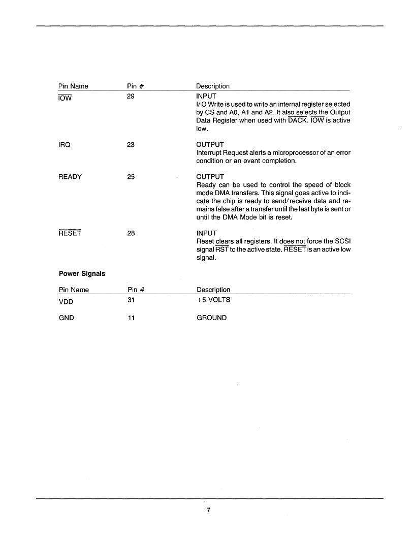
Pin Name Pin # Description
lOW 29 INPUT 110 Write is used to write an internal register selected by CS and AD, A 1 and A2. It also selects the Output Data Register when used with DACK. lOW is active low.
IRQ 23 OUTPUT Interrupt Request alerts a microprocessor of an error condition or an event completion.
READY 25 OUTPUT Ready can be used to control the speed of block mode DMA transfers. This signal goes active to indi-cate the chip is ready to sendl receive data and re-mains false after a transfer until the last byte is sent or until the DMA Mode bit is reset.
RESET 28 INPUT Reset clears all registers. It does not force the SCSI signal RST to the active state. RESET is an active low signal.
Power Signals
Pin Name Pin # Description
VDD 31 +5 VOLTS
GND 11 GROUND
7
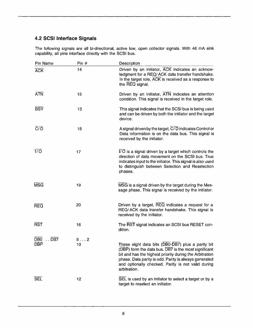
4.2 SCSI Interface Signals
The following signals are all bi-directional, active low, open collector signals. With 48 rnA sink capability, all pins interface directly with the SCSI bus.
Pin Name
CID
DBO ... DB7 DBP
Pin #
14
15
13
18
17
19
20
16
9 ... 2 10
12
Description
Driven by an initiator, ACK indicates an acknowledgment for a REal ACK data transfer handshake. In the target role, ACK is received as a response to the REO signal.
Driven by an initiator, ATN indicates an attention condition. This signal is received in the target role.
This signal indicates that the SCSI bus is being used and can be driven by both the initiator and the target device.
A signal driven by the target, CID indicates Control or Data information is on the data bus. This signal is received by the initiator.
110 is a signal driven by a target which controls the direction of data movement on the SCSI bus. True indicates input to the initiator. This signal is also used to distinguish between Selection and Reselection phases.
MSG is a signal driven by the target during the Message phase. This signal is received by the initiator.
Driven by a target, REO indicates a request for a REal ACK data transfer handshake. This signal is received by the initiator.
The RST signal indicates an SCSI bus RESET condition.
These eight data bits (DBO-DB7) plus a parity bit (DBP) form the data bus. DB7 is the most significant bit and has the highest priority during the Arbitration phase. Data parity is odd. Parity is always generated and optionally checked. Parity is not valid during arbitration.
SEL is used by an initiator to select a target or by a target to reselect an initiator.
8
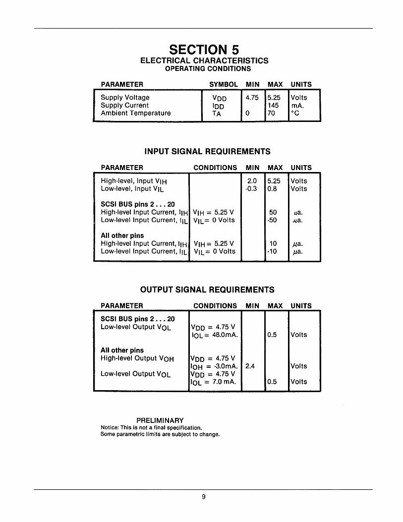
SECTION 5 ELECTRICAL CHARACTERISTICS
OPERATING CONDITIONS
PARAMETER SYMBOL MIN MAX UNITS
Supply Voltage VOO 4.75 5.25 Volts Supply Current 100 145 rnA. Ambient Temperature TA 0 70 °C
INPUT SIGNAL REQUIREMENTS
PARAMETER CONDITIONS MIN MAX UNITS
High-level, Input VIH 2.0 5.25 Volts Low-level, Input VIL -0.3 0.8 Volts
SCSI BUS pins 2 .•. 20 High-level Input Current, IIH VIH = 5.25 V 50 LJa. Low-level Input Current, IlL VIL= 0 Volts -50 .l.Ja.
All other pins High-level Input Current, IIH VIH= 5.25 V 10 ).la. Low-level Input Current, IlL VIL= 0 Volts -10 )la.
OUTPUT SIGNAL REQUIREMENTS
PARAMETER CONDITIONS MIN MAX UNITS
SCSI BUS pins 2 ••. 20 Low-level Output VOL VOO = 4.75 V
IOL= 48.0mA.
All other pins High-level Output VOH VOO = 4.75 V
IOH = -3.0mA. Low-level Output VOL VOO = 4.75 V
IOL = 7.0 rnA.
PRELIMINARY Notice: This is not a final specification. Some parametric limits are subject to change.
9
0.5 Volts
2.4 Volts
0.5 Volts
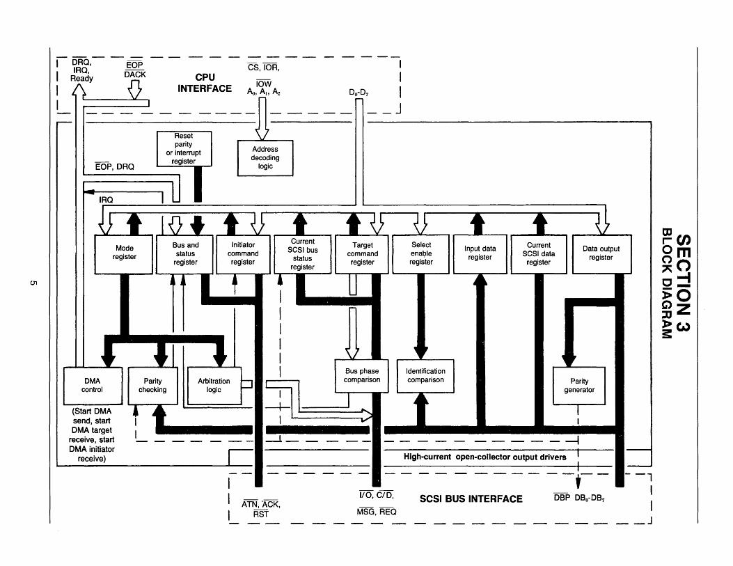
SECTION 6 INTERNAL REGISTERS
6.0 General
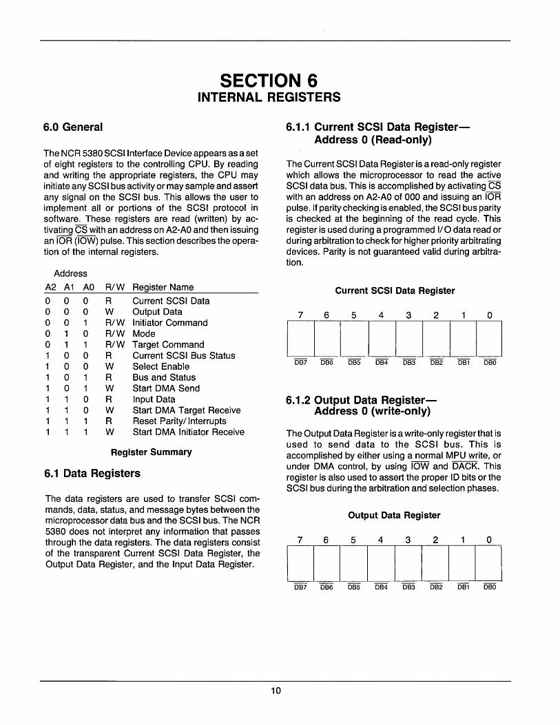
The NCR 5380 SCSI Interface Device appears as a set of eight registers to the controlling CPU. By reading and writing the appropriate registers, the CPU may initiate any SCSI bus activity or may sample and assert any signal on the SCSI bus. This allows the user to implement all or portions of the SCSI protocol in software. These registers are read (written) by activating CS with an address on A2-AO and then issuing an lOR (lOW) pulse. This section describes the operation of the internal registers.
Address
A2 A1 AO
000 000 001 010 o 1 1 100 100 1 0 1 1 0 1 1 1 0 1 1 0 111 111
RlW
R W R/W R/W R/W R W R W R W R W
Register Name
Current SCSI Data Output Data Initiator Command Mode Target Command Current SCSI Bus Status Select Enable Bus and Status Start DMA Send Input Data Start DMA Target Receive Reset Parityl Interrupts Start DMA Initiator Receive
Register Summary
6.1 Data Registers
The data registers are used to transfer SCSI commands, data, status, and message bytes between the microprocessor data bus and the SCSI bus. The NCR 5380 does not interpret any information that passes through the data registers. The data registers consist of the transparent Current SCSI Data Register, the Output Data Register, and the Input Data Register.
10
6.1.1 Current SCSI Data RegisterAddress 0 (Read-only)
The Current SCSI Data Register is a read-only register which allows the microprocessor to read the active SCSI data bus. This is accomplished by activating CS with an address on A2-AO of 000 and issuing an lOR pulse. If parity checking is enabled, the SCSI bus parity is checked at the beginning of the read cycle. This register is used during a programmed 110 data read or during arbitration to check for higher priority arbitrating devices. Parity is not guaranteed valid during arbitration.
Current SCSI Data Register
7 6 5 4 3 2 o
I I I I I I I I I
6.1.2 Output Data RegisterAddress 0 (write-only)
The Output Data Register is a write-only register that is used to send data to the SCSI bus. This is accomplished by either using a normal MPU write, or under DMA control, by using lOW and DACK. This register is also used to assert the proper ID bits or the SCSI bus during the arbitration and selection phases.
Output Data Register
7 6 5 4 3 2 1 o
I I I I I I I I I DB7 DB6 DBS DB4 DB3 DB2 DB 1 DBO
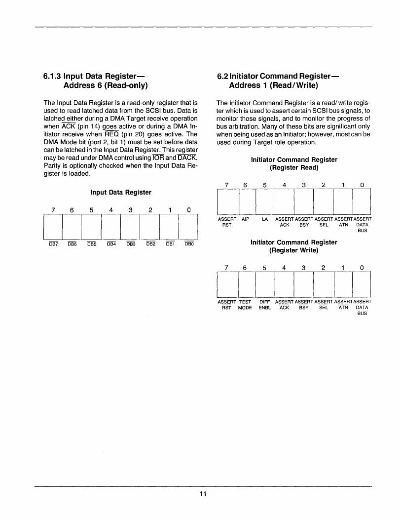
6.1.3 Input Data RegisterAddress 6 (Read-only)
The Input Data Register is a read-only register that is used to read latched data from the SCSI bus. Data is latched either during a DMA Target receive operation when ACK (pin 14) goes active or during a DMA Initiator receive when REO (pin 20) goes active. The DMA Mode bit (port 2, bit 1) must be set before data can be latched in the Input Data Register. This register may be read under DMA control using lOR and DACK. Parity is optionally checked when the Input Data Register is loaded.
Input Data Register
7 6 5 4 3 2 o
6.2 Initiator Command RegisterAddress 1 (Read/Write)
The Initiator Command Register is a read/write register which is used to assert certain SCSI bus signals, to monitor those signals, and to monitor the progress of bus arbitration. Many of these bits are significant only when being used as an Initiator; however, most can be used during Target role operation.
7 6
Initiator Command Register (Register Read)
5 4 3 2 o
I I I I I I I I I I I I I I I I I I
ASSERT AlP LA ASSERT ASSERT ASSERT ASSERT ASSERT RST ACK SSY SEL ATN DATA
SUS
'-0-S7--1--0- S-6-->--0-S-5 --'--0-S4----L-=OS=3:--'--0=S=2:--'---=0=S=1 -'-=o=so=-' In itiator Command Reg ister (Register Write)
7 6 543 2 1 0
I [I I I I III ASSERT TEST OIFF ASSERT ASSERT ASSERT ASSERT ASSERT
RST MODE ENSL ACK SSY SEL ATN DATA SUS
11
The following describes the operation of all bits in the Initiator Command Register.
BIT 7-ASSERT RST
Whenever a one (1) is written to bit 7 of the Initiator Command Register, the RST signal (pin 16) is asserted on the SCSI bus. The RST signal will remain asserted until this bit is reset or until an external RESET (pin 28) occurs. After this bit is set (1), IRQ (pin 23) goes active and all internal logic and control registers are reset (except for the interrupt latch and the ASSERT RST bit). Writing a zero (0) to bit 7 of the Initiator Command Register de-asserts the RST signal. Reading this register simply reflects the status of this bit.
BIT 6-AIP (Arbitration in Progress-read bit)
This bit is used to determine if arbitration is in progress. For this bit to be active, the ARBITRATE bit (port 2, bit 0) must have been set previously. It indicates that a bus free condition has been detected and that the chip has asserted BSY (pin 13) and the contents of the Output Data Register (port 0) onto the SCSI bus. AlP will remain active until the ARBITRATE bit is reset.
BIT 6-TEST MODE (write bit)
This bit may be written during a test environment to disable all output drivers, effectively removing the NCR 5380 from the circuit. Resetting this bit returns the part to normal operation.
BIT 5-LA (Lost Arbitration-read bit)
This bit, when active, indicates that the NCR 5380 detected a bus free condition, arbitrated for use of the bus by asserting BSY (pin 13) and its ID on the data bus and lost arbitration due to SEL (pin 12) being asserted by another bus device. For this bit to be active the ARBITRATE bit (port 2, bit 0) must be active.
BIT 5-DIFF ENBL (Differential Enable-write bit)
This bit is not used in the NCR 5380 and is only meaningful in the NCR 5381, a 48 pin device which supports external differential pair transceivers. DIFF ENBL should only be asserted if the device is physically connected as either an Initiator or as a Target. If enabled, the signal TGS (pin 14-NCR 5381) is asserted if the TARGETMODE bit (port 2, bit 6) is set (1) or the signallGS (pin 12-NCR 5381 ) is asserted if the TARGETMODE bit is reset (0).
12
BIT 4-ASSERT ACK
This bit is used by the bus initiator to assert ACK (pin 14) on the SCSI bus. In order to assert ACK the TARGETMODE bit (port 2, bit 6) must be false. Writing a zero to this bit resets ACK on the SCSI bus. Reading this register simply reflects the status of this bit.
BIT 3-ASSERT BSV
Writing a one (1) into this bit position asserts BSY (pin 13) onto the SCSI bus. Conversely, a zero (0) resets the BSY signal. Asserting BSY indicates a successful selection or reselection and resetting this bit creates a bus disconnect condition. Reading this register simply reflects the status of this bit.
BIT 2-ASSERT SEL
Writing a one (1) into this bit position asserts SEL (pin 12) onto the SCSI bus. SEL is normally asserted after arbitration has been successfully completed. SEL may be de-asserted by resetting this bit to a zero. A read of this register simply reflects the status of this bit.
BIT 1-ASSERT ATN
ATN (pin 15) may be asserted on the SCSI bus by setting this bit to a one (1) if the TARGETMODE bit (port 2, bit 6) is false. ATN is normally asserted by the initiator to request a Message Out bus phase. Note that since ASSERT SEL and ASSERT ATN are in the same register, a select with ATN may be implemented with one MPU write. ATN may be de-asserted by resetting this bit to a zero (0). A read of this register simply reflects the status of this bit.
BIT O-ASSERT DATA BUS
The ASSERT DATA BUS bit, when set, allows the contents of the Output Data Register to be enabled as chip outputs on the signals DBO-DB7. Parity is also generated and asserted on DBP. In the NCR 5381 this bit asserts the DBEN signal (pin 36). Resetting this bit disables the output data bus or the DBEN signal.
When connected as an Initiator, the outputs are only enabled if the TARGETMODE bit (port 2, bit 6) is false, the received signal II 0 (pin 17) is false, and the phase signals (C/D, 110, and MSG) match the contents of the ASSERT CI D, ASSERT 110, and ASSERT MSG in the Target Command Register.
This bit should also be set during DMA send operations.
6.3 Mode Register-Address 2 (Read/Write)
The Mode Register is used to control the operation of the chip. This register determines whether the NCR 5380 operates as an initiator or a target, whether DMA transfers are being used, whether parity is checked, and whether interrupts are generated on various external conditions. This register may be read to check the value of these internal control bits. The following describes the operation of these control bits.
Mode Register
7 6 5 4 3 2 0
II1II1 I D BLOCK TARGET ENABLE ENABLE ENABLE MONITOR DMA ARBIMODE MODE PARITY PARITY EOP BUSY MODE TRATE DMA CHECK- INTER- INTER-
ING RUPT RUPT
BIT 7-BLOCK MODE DMA
The BLOCK MODE DMA bit controls the characteristics of the DMA DRQ-DACK handshake. When this bit is reset (0) and the DMA MODE bit is active (1), the DMA handshake uses the normal interlocked handshake and the rising edge of DACK (pin 26) indicates the end of each byte being transferred. In block mode operation, BLOCK MODE DMA bit set (1) and DMA MODE bit set (1), the end of lOR (pin 24) or lOW (pin 29) signifies the end of each byte transferred and DACK is allowed to remain active throughout the DMA operation. READY (pin 25) can then be used to request the next transfer.
BIT 6-TARGETMODE
The TARGETMODE bit allows the NCR 5380 to operate as either an SCSI bus initiator, bit reset (0), or as an SCSI.bus target device, bit set (1). In orderforthe signals ATN (pin 15) and ACK (pin 14) to be asserted on the SCSI bus, the TARGETMODE bit must be reset (0). In order for the signals C/O, 1/ 0, MSG and REQ to be asserted on the SCSI bus, the TARGETMODE bit must be set (1).
BIT 5-ENABLE PARITY CHECKING
The ENABLE PARITY CHECKING bit determines whether parity errors will be ignored or saved in the parity error latch. If this bit is reset (0), parity will be ignored. Conversely, if this bit is set (1) parity errors will be saved.
13
BIT 4-ENABLE PARITY INTERRUPT
The ENABLE PARITY INTERRUPT bit, when set (1), will cause an interrupt (IRQ) to occur if a parity error is detected. A parity interrupt will only be generated if the ENABLE PARITY CHECKING bit (bit 5) is also enabled (1).
BIT 3-ENABLE EOP INTERRUPT
The ENABLE EOP INTERRUPT, when set (1), causes an interrupt to occur when an EOP (End of Process) signal (pin 27) is received from the DMA controller logic.
BIT 2-MONITOR BUSY
The MONITOR BUSY bit, when true (1), causes an interrupt to be generated for an unexpected loss of BSY (pin 13). When the interrupt is generated due to loss of BSY, the lower 6 bits of the Initiator Command Register are reset (0) and all Signals are removed from the SCSI bus.
BIT 1-DMA MODE
The DMA MODE bit is normally used to enable a DMA transfer and must be set (1) prior to writing ports 5 through 7. Ports 5 through 7 are used to start DMA transfers. The TARGETMODE bit (port 2, bit 6) must be consistent with writes to port 6 and 7 [i.e. set (1) for a write to port 6 and reset (0) for a write to port 7] . The control bit ASSERT DATA BUS (port 1, bit 0) must be true (1) for all DMA send operations. In the DMA mode, REO (pin 20) and ACK (pin 14) are automatically controlled.
The DMA MODE bit is not reset upon the receipt of an EOP signal. Any DMA transfer may be stopped by writing a zero into this bit location, however care must be taken not to cause CS and DACK to be active simultaneously.
BIT O-ARBITRATE
The ARBITRATE bit is set (1) to start the arbitration process. Prior to setting this bit the Output Data Register should contain the proper SCSI device ID value. Only one data bit should be active for SCSI bus arbitration. The NCR 5380 will wait for a bus free condition before entering the arbitration phase. The results of the arbitration phase may be determined by reading the status bits LA and AlP (port 1, bits 5 & 6 respectively) .
14
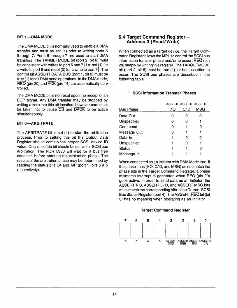
6.4 Target Command RegisterAddress 3 (Read/Write)
When connected as a target device, the Target Command Register allows the MPU to control the SCSI bus information transfer phase andl or to assert REO (pin 20) simply by writing this register. The TARGETMODE bit (port 2, bit 6) must be true (1) for bus assertion to occur. The SCSI bus phases are described in the following table.
SCSI Information Transfer Phases
ASSERT ASSERT ASSERT
Bus Phase 1/0 C/D MSG
Data Out 0 0 0 Unspecified 0 0 1
Command 0 0 Message Out 0 1 1 Data In 1 0 0 Unspecified 0 1
Status 0 Message In
When connected as an Initiator with DMA Mode true, if the phase lines (1/0, C/D, and MSG) do not match the phase bits in the Target Command Register, a phase mismatch interrupt is generated when REO (pin 20) goes active. In order to send data as an Initiator, the ASSERT 1/0, ASSERT CI D, and ASSERT MSG bits must match the corresponding bits in the Current SCSI Bus Status Register (port 4). The ASSERT REO bit (bit 3) has no meaning when operating as an Initiator.
Target Command Register
7 6 5 432 0
LIIIIII D x x x X ASSERT ASSERT ASSERT ASSERT
REO MSG C/O liD
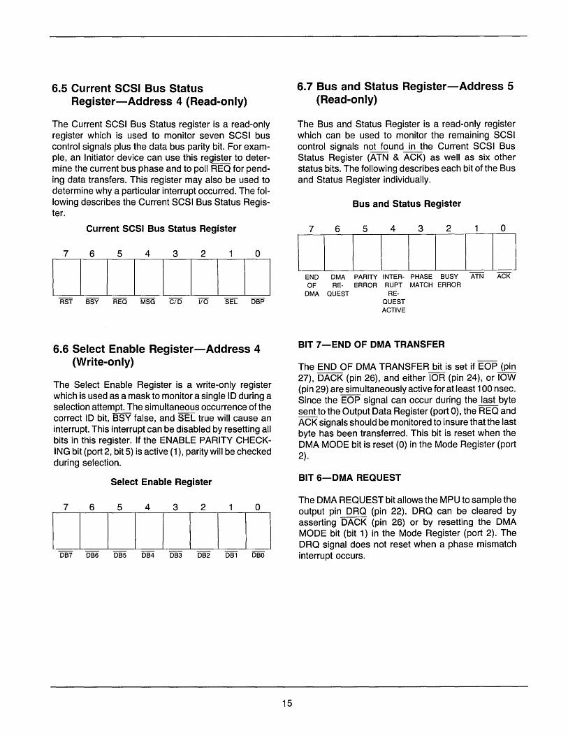
6.5 Current SCSI Bus Status Register-Address 4 (Read-only)
The Current SCSI Bus Status register is a read-only register which is used to monitor seven SCSI bus control signals plus the data bus parity bit. For example, an Initiator device can use this register to determine the current bus phase and to poll REQ for pending data transfers. This register may also be used to determine why a particular interrupt occurred. The following describes the Current SCSI Bus Status Register.
6.7 Bus and Status Register-Address 5 (Read-only)
The Bus and Status Register is a read-only register which can be used to monitor the remaining SCSI control signals not found in the Current SCSI Bus Status Register (ATN & ACK) as well as six other status bits. The following describes each bit of the Bus and Status Register individually.
Bus and Status Register
Current SCSI Bus Status Register 7 6 5 4 3 2 0
.----,--7 ~6 5 -r--4 ~3 --r--2 1--,---.,0 \ \ \ \ \ I I \ ]
l I I I I I I I I END DMA PARITY INTER- PHASE BUSY ATN ACK OF RE- ERROR RUPT MATCH ERROR
DMA QUEST RE-DBP QUEST
6.6 Select Enable Register-Address 4 (Write-only)
The Select Enable Register is a write-only register which is used as a mask to monitor a single ID during a selection attempt. The simultaneous occurrence of the correct ID bit, BSY false, and SEL true will cause an interrupt. This interrupt can be disabled by resetting all bits in this register. If the ENABLE PARITY CHECKING bit (port 2, bit 5) is active (1), parity will be checked during selection.
Select Enable Register
7 6 5 4 3 2 0
[ 1 1 1 I 1 I IJ
15
ACTIVE
BIT 7-END OF DMA TRANSFER
The END OF DMA TRANSFER bit is set if EOP (pin 27), DACK (pin 26), and either lOR (pin 24), or lOW (pin 29) are simultaneously active for at least 100 nsec. Since the EOP signal can occur during the last byte sent to the Output Data Register (port 0), the REQ and ACK signals should be monitored to insure that the last byte has been transferred. This bit is reset when the DMA MODE bit is reset (0) in the Mode Register (port 2).
BIT 6-DMA REQUEST
The DMA REQUEST bit allows the MPU to sample the output pin DRQ (pin 22). DRQ can be cleared by asserting DACK (pin 26) or by resetting the DMA MODE bit (bit 1) in the Mode Register (port 2). The DRQ signal does not reset when a phase mismatch interrupt occurs.
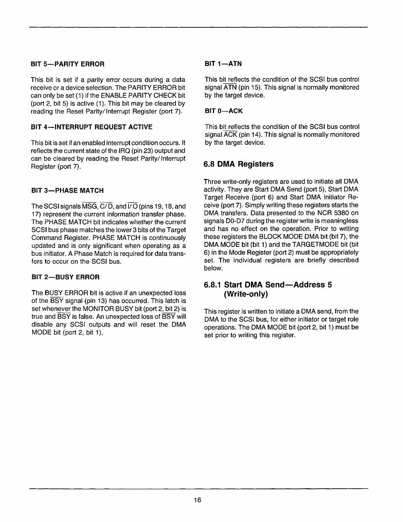
BIT 5-PARITY ERROR
This bit is set if a parity error occurs during a data receive or a device selection. The PARITY ERROR bit can only be set (1) if the ENABLE PARITY CHECK bit (port 2, bit 5) is active (1). This bit may be cleared by reading the Reset Parityl Interrupt Register (port 7).
BIT 4-INTERRUPT REQUEST ACTIVE
This bit is set if an enabled interrupt condition occurs. It reflects the current state of the IRQ (pin 23) output and can be cleared by reading the Reset Parityl Interrupt Register (port 7).
BIT 3-PHASE MATCH
The SCSI signals MSG, CI D, and 110 (pins 19, 18, and 17) represent the current information transfer phase. The PHASE MATCH bit indicates whether the current SCSI bus phase matches the lower 3 bits of the Target Command Register. PHASE MATCH is continuously updated and is only significant when operating as a bus initiator. A Phase Match is required for data transfers to occur on the SCSI bus.
BIT 2-BUSY ERROR
The BUSY ERROR bit is active if an unexpected loss of the BSY signal (pin 13) has occurred. This latch is set whenever the MONITOR BUSY bit (port 2, bit 2) is true and BSY is false. An unexpected loss of BSY will disable any SCSI outputs and will reset the DMA MODE bit (port 2, bit 1).
16
BIT 1-ATN
This bit reflects the condition of the SCSI bus control signal ATN (pin 15). This signal is normally monitored by the target device.
BIT O-ACK
This bit reflects the condition of the SCSI bus control signal ACK (pin 14). This signal is normally monitored by the target device.
6.8 DMA Registers
Three write-only registers are used to initiate all DMA activity. They are Start DMA Send (port 5), Start DMA Target Receive (port 6) and Start DMA Initiator Receive (port 7). Simply writing these registers starts the DMA transfers. Data presented to the NCR 5380 on signals DO-D7 during the register write is meaningless and has no effect on the operation. Prior to writing these registers the BLOCK MODE DMA bit (bit 7), the DMA MODE bit (bit 1) and the TARGETMODE bit (bit 6) in the Mode Register (port 2) must be appropriately set. The individual registers are briefly described below.
6.8.1 Start DMA Send-Address 5 (Write-only)
This register is written to initiate a DMA send, from the DMA to the SCSI bus, for either initiator or target role operations. The DMA MODE bit (port 2, bit 1) must be set prior to writing this register.
6.8.2 Start DMA Target Receive-Address 6 (Write-only)
This register is written to initiate a DMA receive, from the SCSI bustothe DMA, for target operation only. The DMA MODE bit (bit 1) and the TARGETMODE bit (bit 6) in the Mode Register (port 2) must both be set (1) prior to writing this register.
6.8.3 Start DMA Initiator Receive-Address 7 (Write-only)
This register is written to initiate a DMA receive, from the SCSI bus to the DMA, for initiator operation only. The DMA MODE bit (bit 1) must be true (1) and the TARGETMODE bit (bit 6) must be false (0) in the Mode Register (port 2) prior to writing this register.
6.9 Reset Parity/Interrupt-Address 7 (Read-only)
Reading this register resets the PARITY ERROR bit (bit 5), the INTERRUPT REQUEST bit (bit 4) and the BUSY ERROR bit (bit 2) in the Bus and Status Register (port 5).
17
SECTION 7 ON-CHIP SCSI HARDWARE SUPPORT
The NCR 5380 is easy to use because of its simple architecture. The chip allows direct control and monitoring of the SCSI bus by providing a latch for each signal. However, portions of the protocol define timings which are much too quick for traditional microprocessors to control. Therefore, hardware support has been provided for DMA transfers, bus arbitration, phase change monitoring, bus disconnection, bus reset, parity generation, parity checking, and device selection/ reselection.
Arbitration is accomplished using a bus-free filter to continuously monitor BSY. If BSY remains inactive for at least 400 nsec then the SCSI bus is considered free
18
and arbitration may begin. Arbitration will begin if the bus is free, SEL is inactive and the ARBITRATION bit (port 2, bit 0) is active. Once arbitration has begun (BSY asserted), an arbitration delay of 2.2 /Lsec must elapse before the data bus can be examined to determine if arbitration has been won. This delay must be implemented in the controlling software driver.
The NCR 5380 is a clockless device. Delays such as bus free delay, bus set delay and bus settle delay are implemented using gate delays. These delays may differ between devices because of inherent process variations, but are well within the proposed ANSI X3T9.2 specification (Revision 14B).
SECTION 8 INTERRUPTS
The NCR 5380 provides an interrupt output (IRQ) to indicate a task completion or an abnormal bus occurrence. The use of interrupts is optional and may be disabled by resetting the appropriate bits in the Mode Register (port 2) or the Select Enable Register (port 4).
When an interrupt occurs, the Bus and Status Register and the Current SCSI Bus Status Register must be read to determine which condition created the interrupt. IRQ (pin 23) can be reset simply by reading the Reset Parityl Interrupt Register (port 7) or by an external chip reset (RESET active for 200 nsec).
Assuming the NCR 5380 has been properly initialized, an interrupt will be generated if the chip is selected or reselected, if an EOP signal occurs during a DMA transfer, if an SCSI bus reset occurs, if a parity error occurs during a data transfer, if a bus phase mismatch occurs, or if an SCSI bus disconnection occurs.
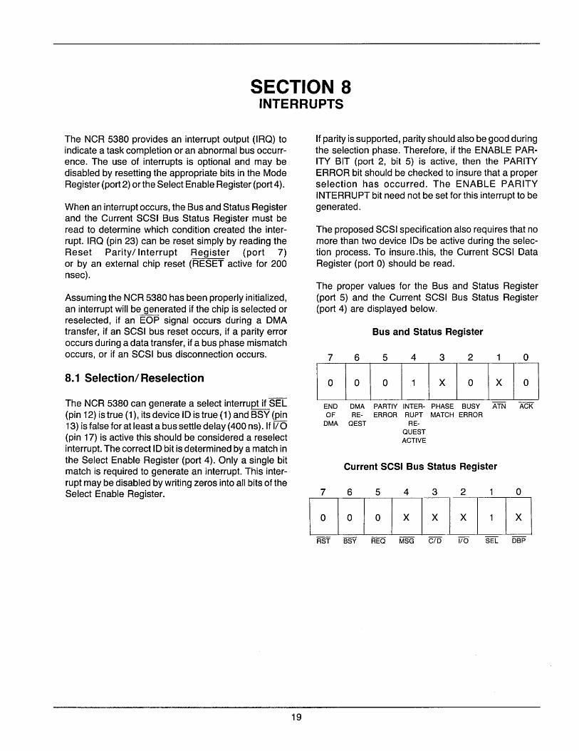
8.1 Selection/ Reselection
The NCR 5380 can generate a select interrupt if SEL (pin 12) is true (1), its device ID is true (1) and BSY (pin 13) is false for at least a bus settle delay (400 ns). If 1/0 (pin 17) is active this should be considered a reselect interrupt. The correct ID bit is determined by a match in the Select Enable Register (port 4). Only a single bit match is required to generate an interrupt. This interrupt may be disabled by writing zeros into all bits of the Select Enable Register.
19
If parity is supported, parity should also be good during the selection phase. Therefore, if the ENABLE PARITY BIT (port 2, bit 5) is active, then the PARITY ERROR bit should be checked to insure that a proper selection has occurred. The ENABLE PARITY INTERRUPT bit need not be set for this interrupt to be generated.
The proposed SCSI specification also requires that no more than two device IDs be active during the selection process. To insure.this, the Current SCSI Data Register (port 0) should be read.
The proper values for the Bus and Status Register (port 5) and the Current SCSI Bus Status Register (port 4) are displayed below.
Bus and Status Register
7 6 5 4 3 2 o
END DMA PARTlY INTER- PHASE BUSY ATN ACK OF RE- ERROR RUPT MATCH ERROR
DMA QEST RE-QUEST ACTIVE
Current SCSI Bus Status Register
7 6 5 4 3 2 0
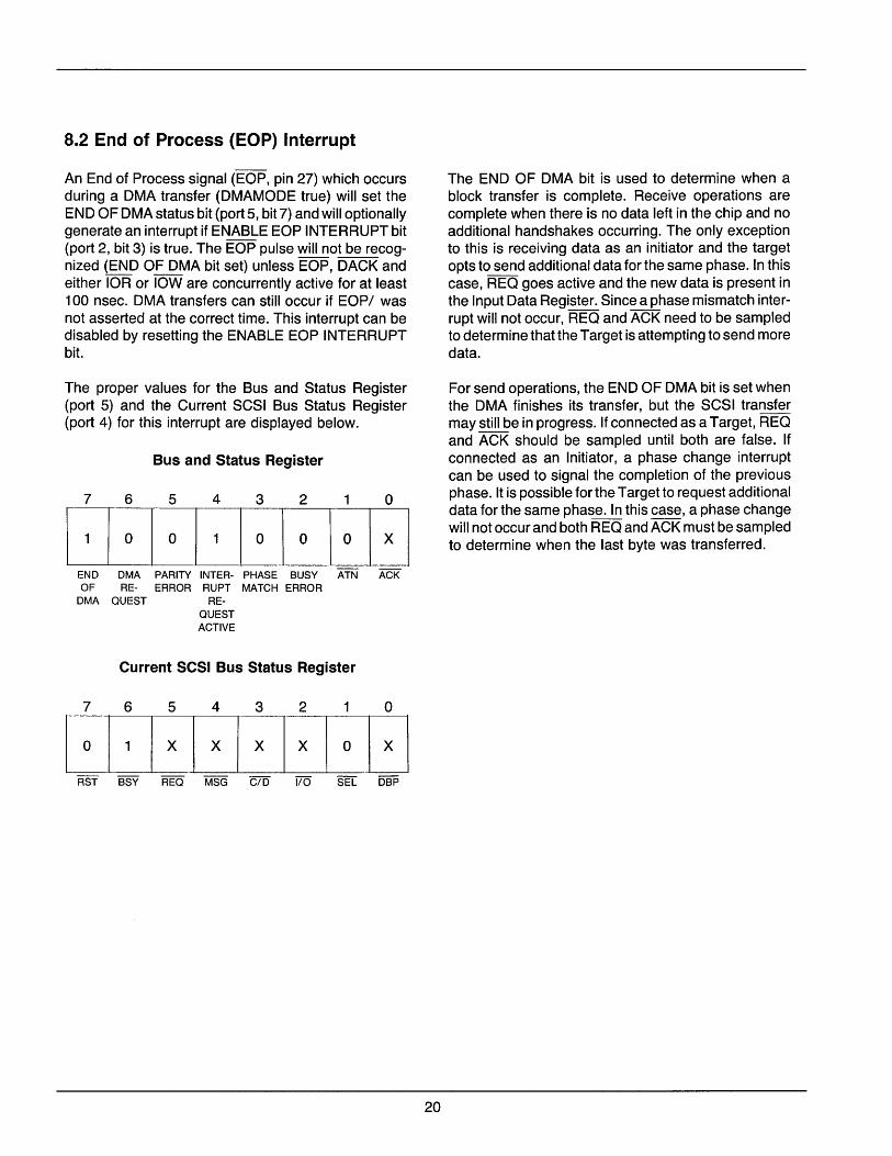
8.2 End of Process (EOP) Interrupt
An End of Process signal (EOP, pin 27) which occurs during a DMA transfer (DMAMODE true) will set the END OF DMA status bit (port 5, bit 7) and will optionally generate an interrupt if ENABLE EOP INTERRUPT bit (port 2, bit 3) is true. The EOP pulse will not be recognized (END OF DMA bit set) unless EOP, DACK and either lOR or lOW are concurrently active for at least 100 nsec. DMA transfers can still occur if EOP/ was not asserted at the correct time. This interrupt can be disabled by resetting the ENABLE EOP INTERRUPT bit.
The proper values for the Bus and Status Register (port 5) and the Current SCSI Bus Status Register (port 4) for this interrupt are displayed below.
7 6
END DMA OF RE-
DMA QUEST
Bus and Status Register
5 4 3 2
PARITY INTER- PHASE BUSY ERROR RUPT MATCH ERROR
RE-QUEST ACTIVE
ATN
Current SCSI Bus Status Register
o
ACK
20
The END OF DMA bit is used to determine when a block transfer is complete. Receive operations are complete when there is no data left in the chip and no additional handshakes occurring. The only exception to this is receiving data as an initiator and the target opts to send additional data for the same phase. In this case, REO goes active and the new data is present in the Input Data Register. Since a phase mismatch interrupt will not occur, REO and ACK need to be sampled to determine that the Target is attempting to send more data.
For send operations, the END OF DMA bit is set when the DMA finishes its transfer, but the SCSI transfer may still be in progress. If connected as a Target, REO and ACK should be sampled until both are false. If connected as an Initiator, a phase change interrupt can be used to signal the completion of the previous phase. It is possible for the Target to request additional data for the same phase. In this case, a phase change will not occur and both REO and ACK must be sampled to determine when the last byte was transferred.
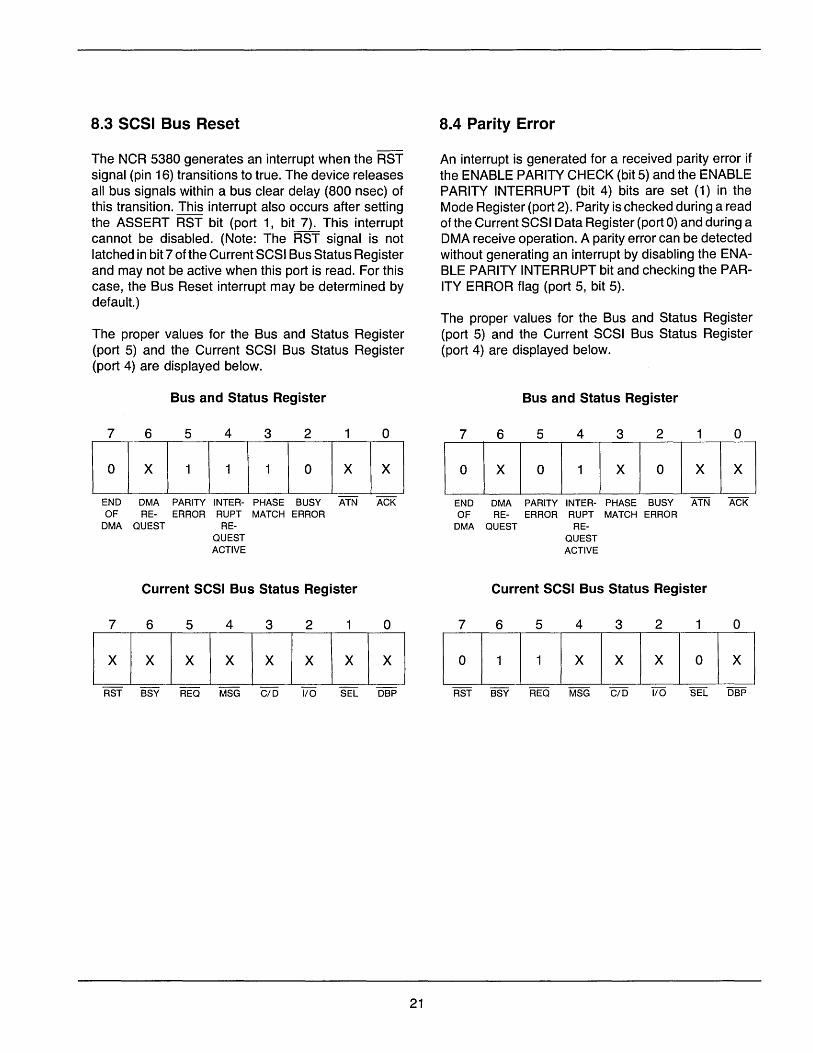
8.3 SCSI Bus Reset
The NCR 5380 generates an interrupt when the RST signal (pin 16) transitions to true. The device releases all bus signals within a bus clear delay (800 nsec) of this transition. This interrupt also occurs after setting the ASSERT RST bit (port 1, bit 7). This interrupt cannot be disabled. (Note: The RST signal is not latched in bit 7 of the Current SCSI Bus Status Register and may not be active when this port is read. For this case, the Bus Reset interrupt may be determined by default.)
The proper values for the Bus and Status Register (port 5) and the Current SCSI Bus Status Register (port 4) are displayed below.
Bus and Status Register
7 6 5 4 3 2 1 a
END DMA PARITY INTER- PHASE BUSY ATN ACK OF RE- ERROR RUPT MATCH ERROR
DMA QUEST RE-QUEST ACTIVE
Current SCSI Bus Status Register
7 6 5 4 3 2 a
RST BSY REQ MSG CID 1/0 SEL DBP
21
8.4 Parity Error
An interrupt is generated for a received parity error if the ENABLE PARITY CHECK (bit 5) and the ENABLE PARITY INTERRUPT (bit 4) bits are set (1) in the Mode Register (port 2). Parity is checked during a read of the Current SCSI Data Register (port 0) and during a DMA receive operation. A parity error can be detected without generating an interrupt by disabling the ENABLE PARITY INTERRUPT bit and checking the PARITY ERROR flag (port 5, bit 5).
The proper values for the Bus and Status Register (port 5) and the Current SCSI Bus Status Register (port 4) are displayed below.
Bus and Status Register
7 6 5 4 3 2 a
END DMA PARITY INTER- PHASE BUSY ATN ACK OF RE- ERROR RUPT MATCH ERROR
DMA QUEST RE-QUEST ACTIVE
Current SCSI Bus Status Register
7 6 5 4 3 2 a
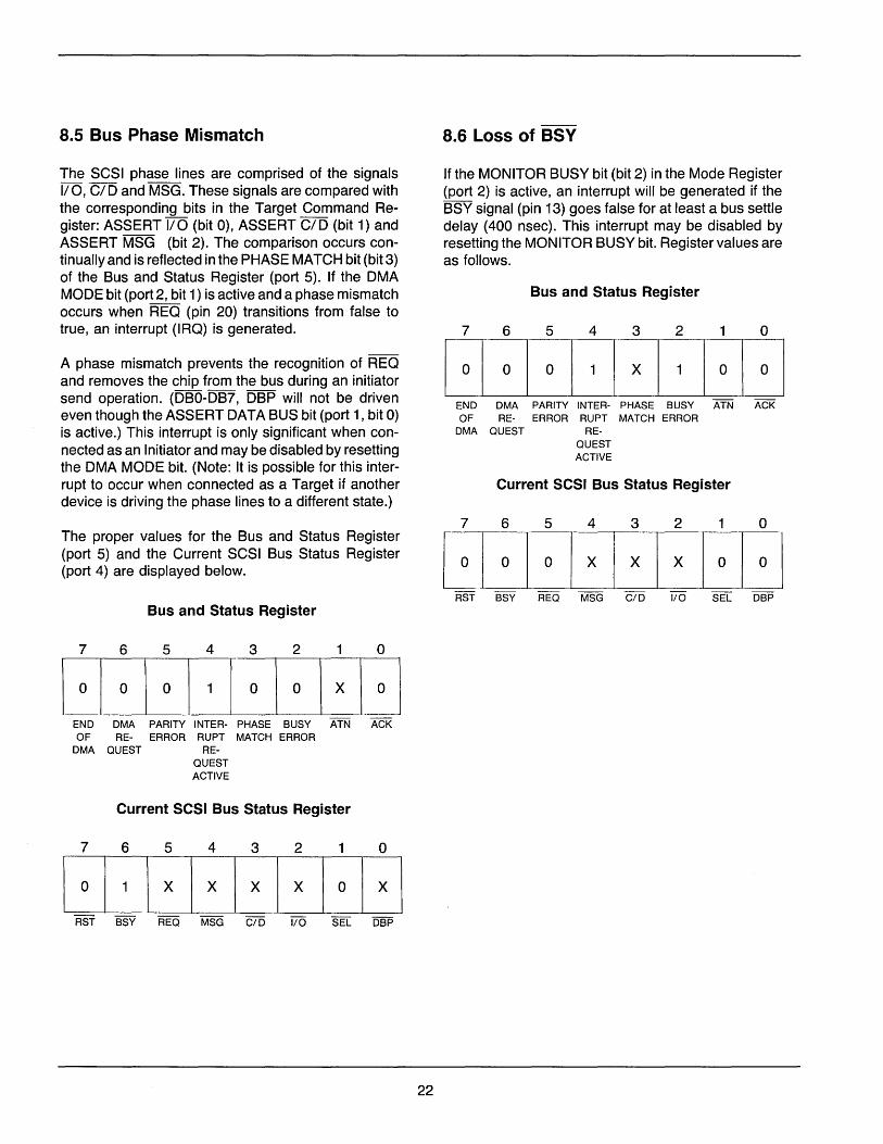
8.5 Bus Phase Mismatch
The SCSI phase lines are comprised of the signals 1/0, CID and MSG. These signals are compared with the corresponding bits in the Target Command Register: ASSERT 110 (bit 0), ASSERT CI D (bit 1) and ASSERT MSG (bit 2). The comparison occurs continuallyand is reflected in the PHASE MATCH bit (bit 3) of the Bus and Status Register (port 5). If the DMA MODE bit (port 2, bit 1) is active and a phase mismatch occurs when REO (pin 20) transitions from false to true, an interrupt (IRO) is generated.
A phase mismatch prevents the recognition of REO and removes the chip from the bus during an initiator send operation. (DBO-DB7, DBP will not be driven even though the ASSERT DATA BUS bit (port 1, bit 0) is active.) This interrupt is only significant when connected as an Initiator and may be disabled by resetting the DMA MODE bit. (Note: It is possible for this interrupt to occur when connected as a Target if another device is driving the phase lines to a different state.)
The proper values for the Bus and Status Register (port 5) and the Current SCSI Bus Status Register (port 4) are displayed below.
Bus and Status Register
7 6 5 4 3 2 0
\o\olo\lo\o\xliJ END DMA PARITY INTER- PHASE BUSY ATN ACK OF RE- ERROR RUPT MATCH ERROR
DMA QUEST RE-QUEST ACTIVE
Current SCSI Bus Status Register
7 6 5 4 3 2 o
22
8.6 Loss of BSY
If the MONITOR BUSY bit (bit 2) in the Mode Register (port 2) is active, an interrupt will be generated if the BSY signal (pin 13) goes false for at least a bus settle delay (400 nsec). This interrupt may be disabled by resetting the MONITOR BUSY bit. Register values are as follows.
Bus and Status Register
END DMA PARITY INTER- PHASE BUSY ATN ACK OF RE- ERROR RUPT MATCH ERROR
DMA QUEST RE-QUEST ACTIVE
Current SCSI Bus Status Register
7 6 5 4 3 2 0
~\ 0 I 0 I X I X \ X \ 0 I 0 \
SECTION 9 RESET CONDITIONS
Three possible reset situations exist with the NCR 5380, as follows:
9.1 Hardware Chip Reset
When the signal RESET / (pin 28) is active for at least 200 nsec, the NCR 5380 device is re-initialized and all internal logic and control registers are cleared. This is a chip reset only and does not create an SCSI bus reset condition.
9.2 SCSI Bus Reset (RST) Received
When an SCSI RST signal (pin 16) is received, an IRQ interrupt is generated and a chip reset is performed. All internal logic and registers are cleared, except for the IRQ interrupt latch and the ASSERT RST bit (bit 7) in
23
the Initiator Command Register (port 1). (Note: The RST signal may be sampled by reading the Current SCSI Bus Status Register (port 4); however, this signal is not latched and may not be present when this port is read.)
9.3 SCSI Bus Reset (RST) Issued
If the CPU sets the ASSERT RST bit (bit 7) in the Initiator Command Register (port 1), the RST signal (pin 16) goes active on the SCSI bus and an internal reset is performed. Again, all internal logic and registers are cleared except for the IRQ interrupt latch and the ASSERT RST bit (bit 7) in the Initiator Command Register (port 1). The RST signal will continue to be active until the ASSERT RST bit is reset or until a hardware reset occurs.
SECTION 10 DATA TRANSFERS
Data may be transferred between SCSI bus devices in one of four modes: Programmed I/O; Normal DMA; Block Mode DMA; or Pseudo DMA. The following sections describe these modes in detail. (Note: For all data transfers operations DACK and CS should never be active simultaneously.)
10.1 Programmed 1/0 Transfers
Programmed I/O is the most primitive form of data transfer. The REO (pin 20) and ACK (pin 14) handshake signals are individually monitored and asserted by reading and writing the appropriate register bits. This type of transfer is normally used when transferring small blocks of data such as command blocks or message and status bytes.
An Initiator send operation would begin by setting the C/O, I/O, and MSG bits in the Target Command Register to the correct state so that a phase match exists. In addition to the phase match condition, it is necessary for the ASSERT DATA BUS bit (port 1, bit 0) to be true and the received I/O signal to be false for the 5380 to send data.
For each transfer, the data is loaded into the Output Data Register (port 0). The MPU then waits for the REO bit (port 4, bit 5) to become active. Once REO goes active the PHASE MATCH bit (port 5, bit 3) is checked and the ASSERT ACK bit (port 1, bit 4) is set. The REO bit is sampled until it becomes false and the MPU resets the ASSERT ACK bit to complete the transfer.
24
10.2 Normal DMA Mode
DMA transfers are normally used for large block transfers. The SCSI chip outputs a DMA request (ORO - pin 22) whenever it is ready for a byte transfer. External DMA logic uses this ORO signal to generate DACK and an lOR or an lOW pulse to the NCR 5380. ORO goes inactive when DACK is asserted and DACK goes inactive sometime after the minimum read or write pulse width. This process is repeated for every byte. For this mode, DACK should not be allowed to cycle unless a transfer is taking place.
Refer to Section 10.5 for information on halting a DMA transfer.
10.3 Block Mode DMA
Some popular DMA controllers such as the Intel 8237 provide a block mode DMA transfer. This type of transfer allows the DMA controller to transfer blocks of data without relinquishing the use of the data bus to the MPU after each byte is transferred. Thus, faster transfer rates are achieved by eliminating the repetitive access and release of the MPU bus.
If the BLOCK MODE DMA bit (port 2, bit 7) is active, the NCR 5380 will begin the transfer by asserting ORO. The DMA controller then asserts DACK for the remainder of the block transfer. ORO goes inactive after detecting DACK and also remains inactive for the duration of the transfer. The READY output (pin 25) is used to control the transfer rate.
Non-block mode DMA transfers end when DACK goes false, whereas block mode transfers end when lOR or lOW becomes inactive. Since this is the case, DMA transfers may be started sooner in a block mode transfer.
To obtain optimum performance in block mode operation, the DMA logic may optionally use the normal DMA mode interlocking handshake. READY is still available to throttle the DMA transfer, but DRO is 30 to 40 nsec faster than READY and may be used to start the cycle sooner.
The methods described in Section 10.5 "Halting A DMA Operation" apply for all DMA operations.
10.4 Pseudo DMA Mode
To avoid the tedium of monitoring and asserting the request! acknowledge handshake signals for programmed 110 transfers, the system may be designed to implement a pseudo DMA mode. This mode is implemented by programming the NCR 5380 to operate in the DMA mode, but using the MPU to emulate the DMA handshake. DRO (pin 22) may be detected by polling the DMA REO bit (bit 6) in the Bus and Status Register (port 5), by sampling the signal through an external port or by using it to generate an MPU interrupt. Once DRO is detected, the MPU can perform a DMA port read or write data transfer. This MPU readl write is externally decoded to generate the appropriate DACK and lOR or lOW signals.
Often, external decoding logic is necessary to generate the NCR 5380 CS signal. This same logic may be used to generate DACK at no extra system cost and provide an increased performance in programmed 10 transfers.
10.5 Halting A DMA Operation
The EOP signal is not the only way to halt a DMA transfer. A bus phase mismatch or a reset of the DMA MODE bit (port 2, bit 1) can also terminate a DMA cycle for the current bus phase.
25
10.5.1 Using the EOP Signal
If EOP is used, it should be asserted for at least 100 nsec while DACK and lOR or lOW are simultaneously active. Note, however, that if lOR or lOW is not active an interrupt will be generated, but the DMA activity will continue. The EOP signal does not reset the DMA MODE bit. Since the EOP signal can occur during the last byte sent to the Output Data Register (port 0), the REO and ACK signals should be monitored to insure that the last byte has transferred.
10.5.2 Bus Phase Mismatch Interrupt
A bus phase mismatch interrupt may be used to halt the transfer if operating as an Initiator. Using this method frees the host from maintaining a data length counter and frees the DMA logic from providing the EOP signal. If performing an initiator send operation, the NCR 5380 requires DACK to cycle before ACK goes inactive. Since phase changes cannot occur if ACK is active, either DACK must be cycled after the last byte is sent or the DMA MODE bit must be reset in order to receive the phase mismatch interrupt.
10.5.3 Resetting the DMA MODE Bit
A DMA operation may be halted at any time simply by resetting the DMA MODE bit. It is recommended that the DMA MODE bit be reset after receiving an EOP or bus phase mismatch interrupt. The DMA MODE bit must then be set before writing any of the start DMA registers for subsequent bus phases.
If resetting the DMA MODE bit is used instead of EOP for Target role operation, then care must be taken to reset this bit at the proper time. If receiving data as a target device, the DMA MODE bit must be reset once the last DRO is received and before DACK is asserted to prevent an additional REO from occurring. Resetting this bit causes DRO to go inactive. However, the last byte received remains in the Input Data Register and may be obtained either by performing a normal MPU read or by cycling DACK and lOR. In most cases EOP is easier to use when operating as a Target device.
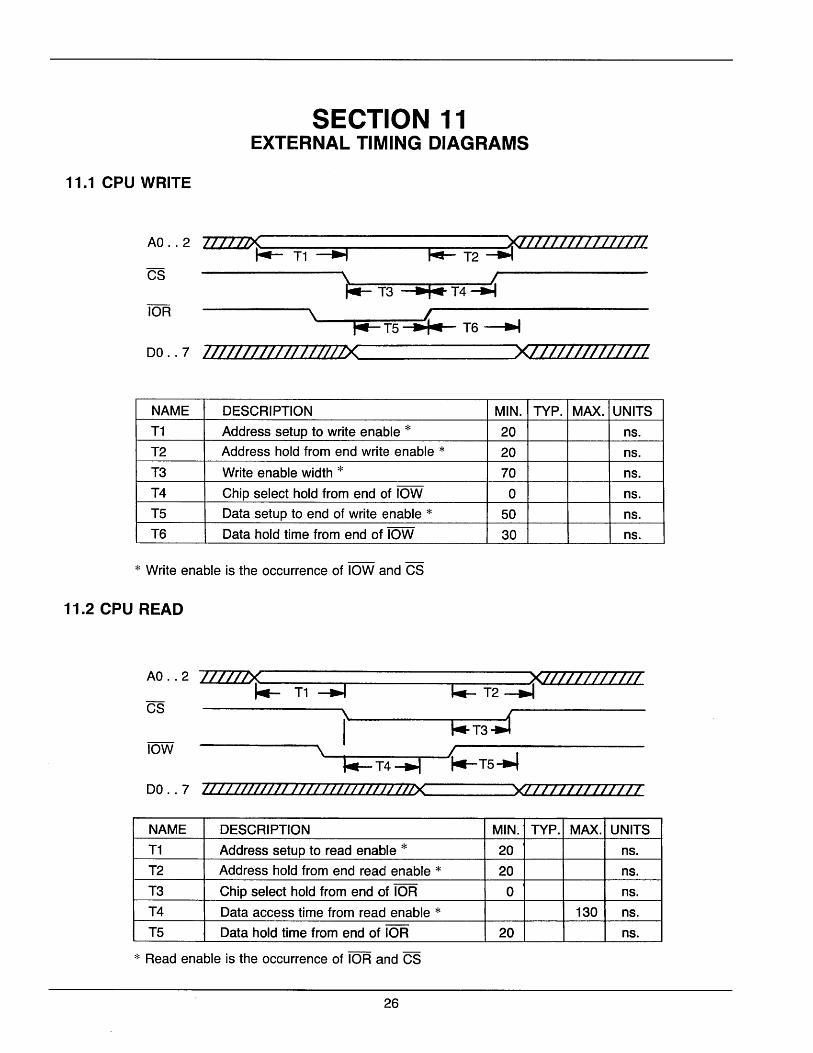
11.1 CPU WRITE
SECTION 11 EXTERNAL TIMING DIAGRAMS
AO .. 2 77777Z1-4---T-1--~~~-------r~~--T2--~777777777777711
~ T3
\ ,..- T5 -14 T6 ~
DO .. 7 IOOZZOZOZZWIX ________ --'X77111/oZZ0Z1
NAME DESCRIPTION MIN. TYP. MAX. UNITS
T1 Address setup to write enable * 20 ns.
T2 Address hold from end write enable * 20 ns.
T3 Write enable width * 70 ns.
T4 Chip select hold from end of lOW 0 ns.
T5 Data setup to end of write enable * 50 ns.
T6 Data hold time from end of lOW 30 ns.
* Write enable is the occurrence of lOW and CS
11.2 CPU READ
AO .. 2 777OZX _____ -r--____ ---.___ xllllllllllll ~ T1 =+I ~T2~
f ~T3~ \'----t~r----T-4-+1---r----Ji--T5 ~
DO .. 7 7777777777777777777777777277lX _____ ..... XZ7777777777777
NAME DESCRIPTION MIN. TYP. MAX. UNITS
T1 Address setup to read enable * 20 ns.
T2 Address hold from end read enable * 20 ns.
T3 Chip select hold from end of lOR 0 ns.
T4 Data access time from read enable * 130 ns.
T5 Data hold time from end of lOR 20 ns.
* Read enable is the occurrence of lOR and CS
26
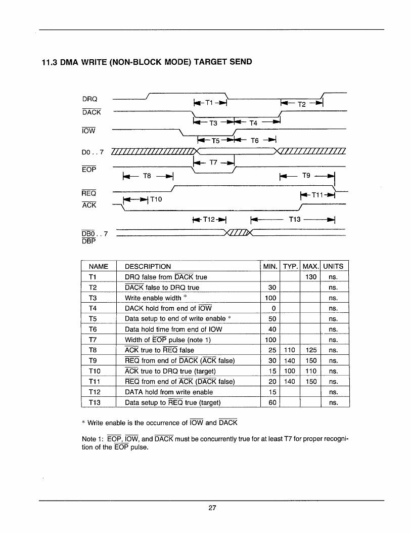
11.3 DMA WRITE (NON-BLOCK MODE) TARGET SEND
DRO
DACK
_____ I
\
\ ~T1~~------~----
1 ~T2~
\ I !;i=T3 .. I~ T4 ~
i4= T5 ~ T6----1
DO .. 7 OlllllllllllllllllllX'-___ ~----'XIII II IIIIII 1111
~T7=+1 --~----T-8-~----~\ 1~--------~----T-9-~-----
REO ----------~I ~T11~~ ACK ~J-1 .... 1 T1 0
DBO .. 7 DBP
NAME
T1
T2
T3
T4
T5
T6
T7
T8
T9
T10
T11
T12
T13
',-. --------------------------__ ----'1 i4-T12~ J.-I~t---- T13 ----.... ~~I
-------------~--------------
DESCRIPTION MIN. TYP. MAX. UNITS
DRO false from DACK true 130 ns.
DACK false to DRO true 30 ns.
Write enable width * 100 ns.
DACK hold from end of lOW 0 ns.
Data setup to end of write enable * 50 ns.
Data hold time from end of lOW 40 ns.
Width of EOP pulse (note 1) 100 ns. - --ACK true to REO false 25 110 125 ns.
REO from end of DACK (ACK false) 30 140 150 ns.
ACK true to DRO true (target) 15 100 110 ns.
REO from end of ACK (DACK false) 20 140 150 ns.
DATA hold from write enable 15 ns.
Data setup to REO true (target) 60 ns.
* Write enable is the occurrence of lOW and DACK
Note 1: EOP, lOW, and DACK must be concurrently true for at least T7 for proper recognition of the EOP pulse.
27
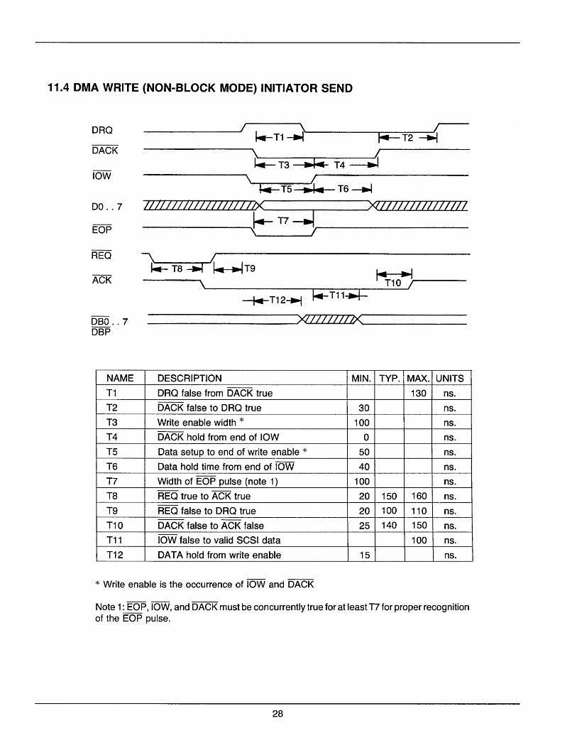
11.4 DMA WRITE (NON-BLOCK MODE) INITIATOR SEND
DRO
DACK
DO .. 7
EOP
DBO .. 7 DBP
NAME
T1
T2
T3
T4
T5
T6
T7
T8
T9
T10
T11
T12
/ \ I ----------~ ~T1~~------~~--~T2~~~
\ I ~T3 ~ .. T4~
\ l'4=T5 ..1: T6 ~ IZlIllllIllllllllllt< >QIIIIIII17777177
~T7~ --------------~\ ,-----------------------
f.: T8 --.o! 1: .IT9 I.. I ------~\~ ______________ ~------~--~-T-1-0~~/~-------
-f4-T12..., 14= T11+i=
____________________ --J>e1111711t<~ ______________ _
DESCRIPTION MIN. TYP. MAX. UNITS
DRO false from DACK true 130 ns.
DACK false to DRO true 30 ns.
Write enable width * 100 ns.
DACK hold from end of lOW 0 ns.
Data setup to end of write enable * 50 ns.
Data hold time from end of lOW 40 ns.
Width of EOP pulse (note 1) 100 ns.
REO true to ACK true 20 150 160 ns.
REO false to DRO true 20 100 110 ns.
DACK false to ACK false 25 140 150 ns.
lOW false to valid SCSI data 100 ns.
DATA hold from write enable 15 ns.
* Write enable is the occurrence of lOW and DACK
Note 1: EOP, lOW, and DACK must be concurrently true for at least T7 for proper recognition of the EOP pulse.
28
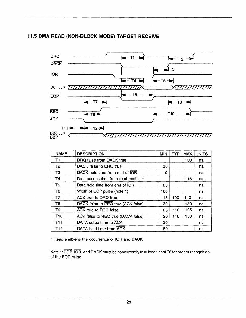
11.5 DMA READ (NON-BLOCK MODE) TARGET RECEIVE
DRO / \ ~T1~
DACK \
I ~ T2 ::::;t I '--___ ,-~_-..J~ T3
I~-------------------~~----~~~T5~
lOR \ I t4=T4~
::~ .. 77 ...,.7...,..I-r-l.,....IF"'lI~I-rll...,.I.,...I.,....Ir-:l,...,Z-rZ7.,.7"7"'7.,....17""l1,...,I.....,e...,-r.,...77""l;r-7~...,..Ib< __ --IJ .. ,. ____ )q~_7~_7 ..... 7~7:Z_Z~Z~ZT"'l/_~Z_~Z_7~Z~7
\ I t-- T8 ~
/ ~T9:j;l t----- T10
..)~---
\~----------------------~I T111~ .. I- T12-.l
8~~·· 7 < >qllllllllllllllllllllllllllllll/llllZlllllZ
NAME DESCRIPTION MIN. TYP. MAX. UNITS
T1 DRO false from DACK true 130 ns.
T2 DACK false to DRO true 30 ns.
T3 DACK hold time from end of lOR 0 ns.
T4 Data access time from read enable * 115 ns.
T5 Data hold time from end of lOR 20 ns.
T6 Width of EOP pulse (note 1) 100 ns.
T7 ACK true to DRO true 15 100 110 ns.
T8 DACK false to REO true (ACK false) 30 150 ns.
T9 ACK true to REO false 25 110 125 ns.
T10 ACK false to REO true (DACK false) 20 140 150 ns.
T11 DATA setup time to ACK 20 ns.
T12 DATA hold time from ACK 50 ns.
* Read enable is the occurrence of lOR and DACK
Note 1: EOP, lOR, and DACK must be concurrently true for at least T6 for proper recognition of the EOP pulse.
29
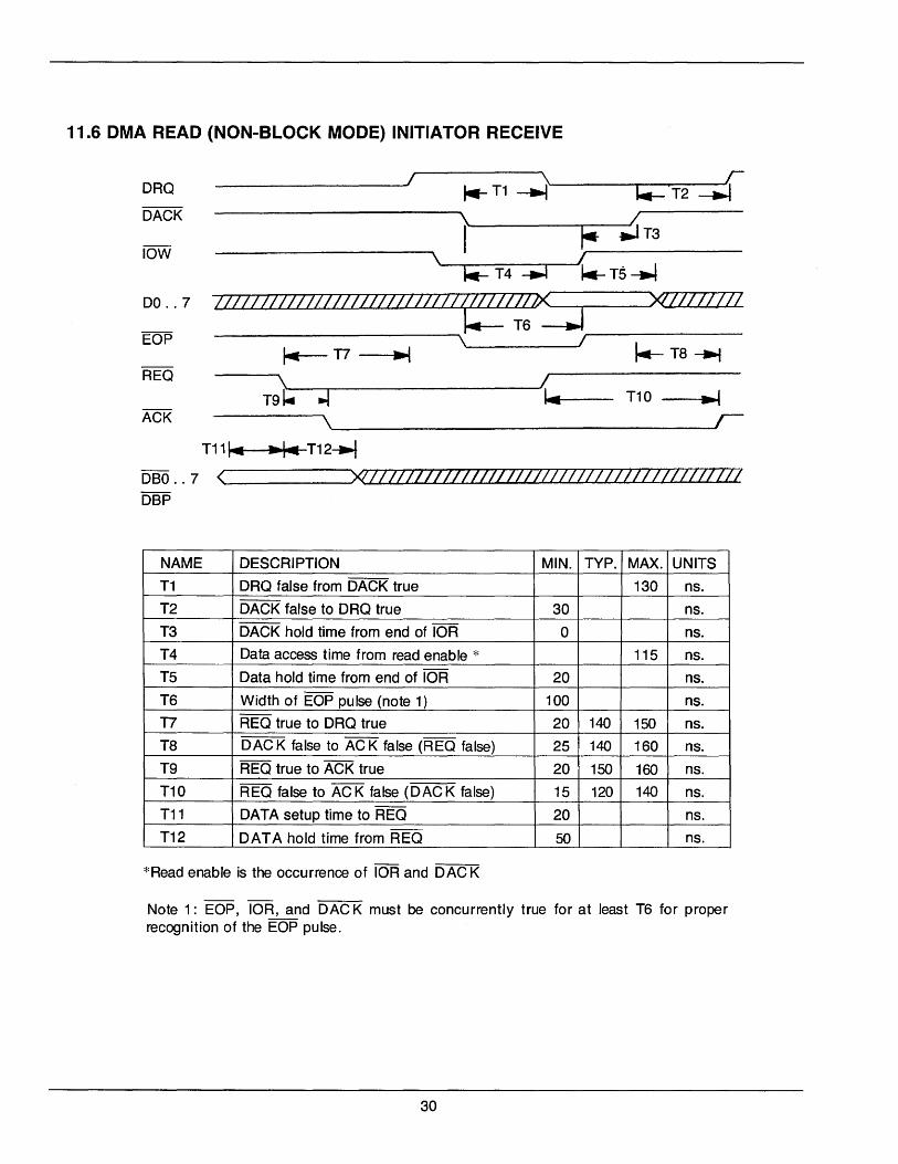
11.6 DMA READ (NON-BLOCK MODE) INITIATOR RECEIVE
ORO
DACK
00 .. 7
__________________ 1 \ r ~T1~~----~~~~T2-~
I ~ ;iT3 \ /~--------------
~~~-T-4-~~--~T5~
ZZZZZZZZZZZZZZZZZZZZZZZZZZZ~;ShK ---J-~------J>eZZZZZZ17
\ / k-T8~
T9);~-;f-r------------{"~I---- T10 ~ \~ ____________________________________ r--
T11~ ... ,. T12-.f
DBO .. 7 <'-_____ -.JXlZZZZZ////////OZZ/ZZZZZZZZZZZZZ77ZZZ0ZZ1 DBP
NAME DESCRIPTION MIN. TYP. MAX. UNITS
T1 ORO false from DACK true 130 ns.
T2 DACK false to ORO true 30 ns.
T3 DACK hold time from end of lOR 0 ns.
T4 Data access time from read enable * 115 ns.
T5 Data hold time from end of lOR 20 ns.
T6 Width of EOP pulse (note 1) 100 ns.
T7 REO true to ORO true 20 140 150 ns.
T8 DAC K false to AC K false (REO false) 25 140 160 ns.
T9 REO true to ACK true 20 150 160 ns.
T10 REO false to AC K false (DAC K false) 15 120 140 ns.
T11 DATA setup time to REO 20 ns.
T12 DATA hold time from REO 50 ns.
*Read enable is the occurrence of lOR and DAC K
Note 1: EOP, lOR, and DAC K must be concurrently true for at least T6 for proper recognition of the EOP pulse.
30
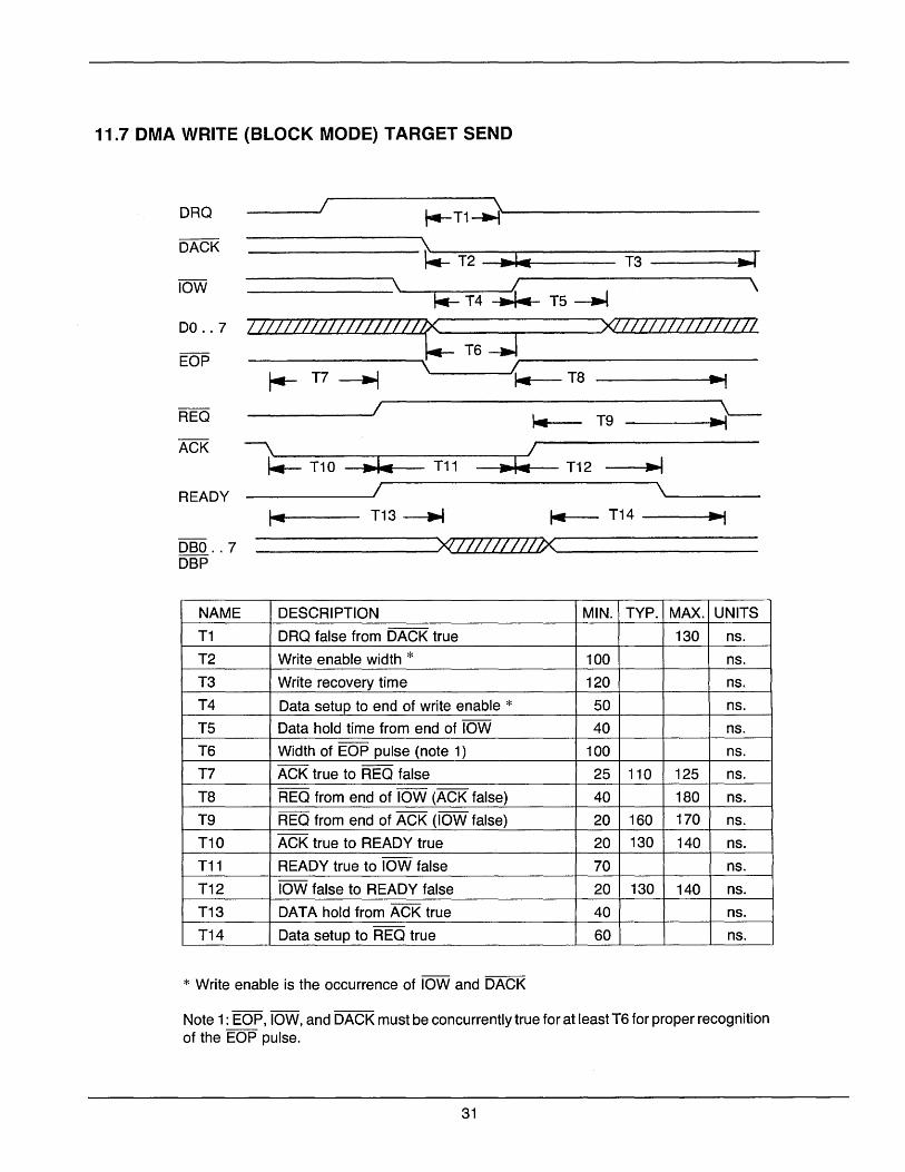
11.7 DMA WRITE (BLOCK MODE) TARGET SEND
ORO
DACK
00 .. 7
EOP
REO
ACK
READY
DBO .. 7 DBP
NAME
T1
T2
T3
T4
T5
T6
T7
T8
T9
T10
T11
T12
T13
T14
___ -J1 \ ~T1~~-------------------
---------------~~~~--------------------~ ~ T2 ---I.~I.I------ T3 ----... ~~ \ 1 \
------ '----r-~-T-4--~-1-4 T5--.t
ZZL7ZZZLZZZOZZZZZt:'--'--T-6-~~---~XlZZZZZZZZZZZZZO
I--- T7 ~ \ / .... ~'--- T8
_____ --'1 T9 ------I ... ~
\ J 14= T10 .. I. T11 .1. T12 --I
J \
I~ T13~ 14 T14 ~I
______________ X'ZOZOzwx'--_________ _
DESCRIPTION MIN. TYP. MAX. UNITS
ORO false from DACK true 130 ns.
Write enable width * 100 ns.
Write recovery time 120 ns.
Data setup to end of write enable * 50 ns.
Data hold time from end of lOW 40 ns.
Width of EOP pulse (note 1) 100 ns.
ACK true to REO false 25 110 125 ns.
REO from end of lOW (ACK false) 40 180 ns.
REO from end of ACK (lOW false) 20 160 170 ns.
ACK true to READY true 20 130 140 ns. -
READY true to lOW false 70 ns.
lOW false to READY false 20 130 140 ns.
OAT A hold from ACK true 40 ns.
Data setup to REO true 60 ns.
* Write enable is the occurrence of lOW and DACK
Note 1: EOP , lOW, and DACK must be concurrently true for at least T6 for proper recognition of the EOP pulse.
31
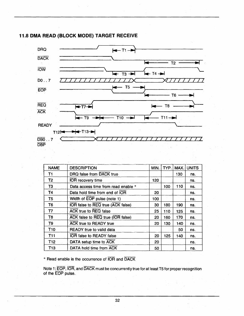
11.8 DMA READ (BLOCK MODE) TARGET RECEIVE
ORO
DACK
00 .. 7
I ~T1=4 \
14 T2 ~I \
J400 T3 -..:I / '-~ T4-.1
I Z 7 Z 7 7 7 7 7 7 7 7 Z 7 JX'-________ Xl! 7 7 7 7 7 7 7 r-- T5 ---.,
----------------~\ 1--------------------~ ... II----- T6 ----I~ .. I
I "'T7~ 14-- T8 '-------I~~I
--...... , i4=T9 _14 ------~----------~--~I
T10 ~ ~ T11....1
READY I \'-----T12t4-14 T13~
DBO .. 7 <'-____ ~)q 7 7 7 7 7 7 7 7 7 7 7 7 7 7 7 7 7 Z 7 7 7 DBP
NAME DESCRIPTION MIN. TYP. MAX. UNITS
T1 ORO false from DACK true 130 ns.
T2 lOR recovery time 120 ns.
T3 Data access time from read enable * 100 110 ns.
T4 Data hold time from end of lOR 20 ns.
T5 Width of EOP pulse (note 1) 100 ns.
T6 lOR false to REO true (ACK false) 30 180 190 ns.
T7 ACK true to REO false 25 110 125 ns.
T8 ACK false to REO true (lOR false) 20 160 170 ns.
T9 ACK true to READY true 20 130 140 ns.
T10 READY true to valid data 50 ns.
T11 lOR false to READY false 20 125 140 ns.
T12 DATA setup time to ACK 20 ns.
T13 DATA hold time from ACK 50 ns.
* Read enable is the occurrence of lOR and DACK
Note 1: EOP, lOR, and DACK must be concurrently true for at least T5 for proper recognition of the EOP pulse.
32
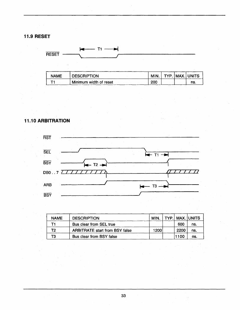
11.9 RESET
1-. T1 ~ RESET \~ _____ ....JI
NAME DESCRIPTION
T1 Minimum width of reset
11.10 ARBITRATION
__ ---.1/
MIN. TYP. MAX. UNITS
200 ns.
\ 1~4--T-1-~~---------
BSY 1-- T2 ...J-----------1 DBO .. 7 z:J 777 7 7 7 71 17 7 7 7 7 77
ARB --------------, \ t4- T3 ~'-------
--------------------------_/
NAME DESCRIPTION MIN. TYP. MAX. UNITS
T1 Bus clear from SEL true 600 ns.
T2 ARBITRATE start from BSY false 1200 2200 ns.
T3 Bus clear from BSY false 1100 ns.
33
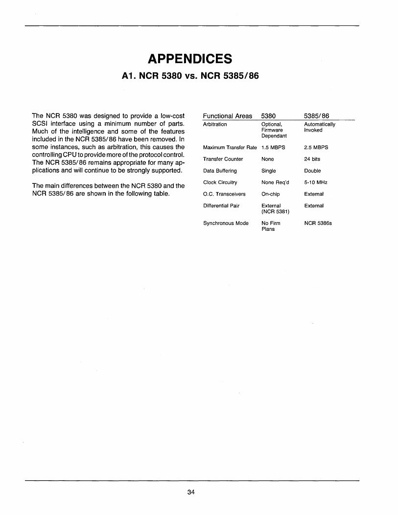
APPENDICES A1. NCR 5380 vs. NCR 5385/86
The NCR 5380 was designed to provide a low-cost Functional Areas 5380 5385/86 SCSI interface using a minimum number of parts. Arbitration Optional, Automatically
Much of the intelligence and some of the features Firmware Invoked
included in the NCR 5385/86 have been removed. In Dependant
some instances, such as arbitration, this causes the Maximum Transfer Rate 1.5 MBPS 2.5 MBPS
controlling CPU to provide more of the protocol control. Transfer Counter None 24 bits
The NCR 5385/86 remains appropriate for many ap-plications and will continue to be strongly supported. Data Buffering Single Double
The main differences between the NCR 5380 and the Clock Circuitry None Req'd 5-10 MHz
NCR 5385/86 are shown in the following table. D.C. Transceivers On-chip External
Differential Pair External External (NCR 5381)
Synchronous Mode No Firm NCR 5386s Plans
34

A2. FLOWCHARTS/SOFTWARE
Flowcharts and sample software drivers are provided as a guideline to facilitate your firmware development. Firmware will vary depending on the application and the level of the SCSI protocol being supported.
35
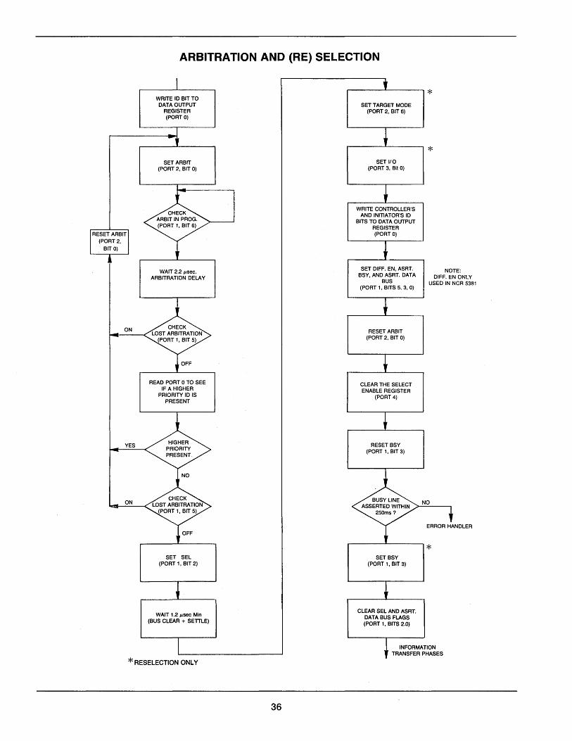
ARBITRATION AND (RE) SELECTION
ON
YES
ON
WRITE 10 BIT TO DATA OUTPUT
REGISTER (PORTO)
SET ARB IT (PORT 2, BIT 0)
WAIT 2.2 ILsec. ARBITRATION DELAY
READ PORT 0 TO SEE IF A HIGHER
PRIORITY 10 IS PRESENT
SET SEL (PORT 1, BIT 2)
WAIT 1.2lLsec Min (BUS CLEAR + SETTLE)
* RESELECTION ONLY
36
~ ______ -L ______ --, * SET TARGET MODE
(PORT 2, BIT 6)
SET 1/0 (PORT 3, Bit 0)
WRITE CONTROLLER'S AND INITIATOR'S 10
BITS TO DATA OUTPUT REGISTER (PORT 0)
SET DIFF. EN, ASRT.
*
NOTE: BSY, AND ASRT. DATA
BUS DIFF. EN ONLY
USED IN NCR 5381 (PORT 1, BITS 5, 3, 0)
RESET ARBIT (PORT 2, BIT 0)
CLEAR THE SELECT ENABLE REGISTER
(PORT 4)
RESET BSY (PORT 1, BIT 3)
SET BSY (PORT 1, BIT 3)
CLEAR SEL AND ASRT. DATA BUS FLAGS (PORT 1, BITS 2.0)
INFORMATION TRANSFER PHASES
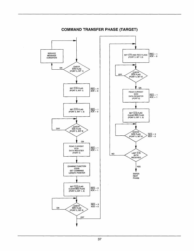
SERVICE MESSAGE
CONDITION
OFF
ON
COMMAND TRANSFER PHASE (TARGET)
SET C/O FLAG (PORT 3, BIT 1)
SET C/O FLAG (PORT 3, BIT 1, 3)
READ CURRENT SCSI
DATA REGISTER (PORT 0)
EXAMINE FUNCTION CODE
SET COMMAND LENGTH POINTER
SETC/D FLAG CLEAR-REO FLAG (PORT 3, BIT 1, 3)
OFF
REO = 0 ACK = 0
REO = 1 ACK = 0
REO = 1 ACK = 1
REO = 0 ACK = 1
37
OFF
NO
SET C/ D AND REO FLAGS REO = 1 (PORT 3, BIT 1,3) ACK = 0
READ CURRENT SCSI
DATA REGISTER (PORT 0)
SET C/D FLAG CLEAR REO FLAG (PORT 3, BIT 1, 3)
ENTER NEXT PHASE
REO = 1 ACK = 1
REO = 0 ACK = 0
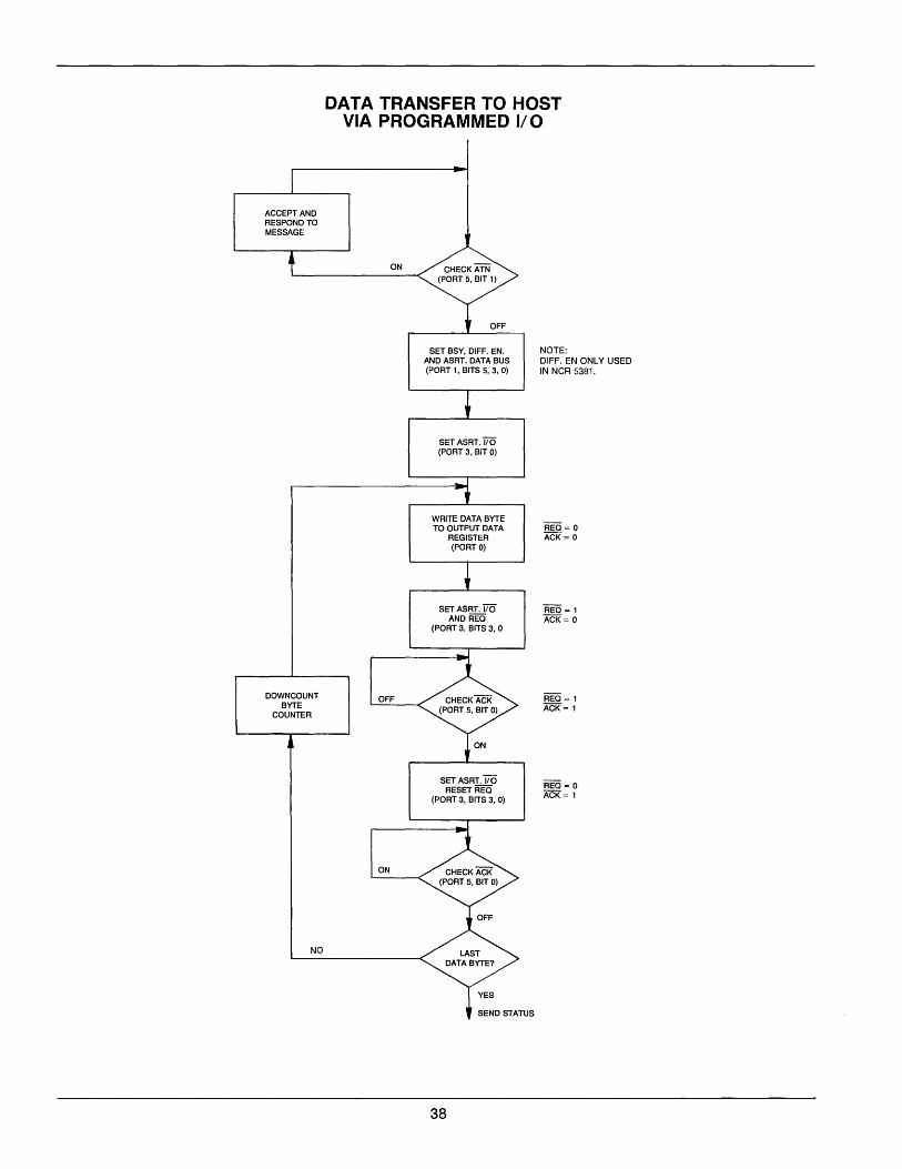
ACCEPT AND RESPOND TO MESSAGE
DOWNCOUNT BYTE
COUNTER
NO
DATA TRANSFER TO HOST VIA PROGRAMMED 1/0
ON
OFF
ON
SET BSY, DIFF. EN. AND ASRT. DATA BUS (PORT 1, BITS 5, 3, 0)
SET ASRT.//O (PORT 3, BIT 0)
WRITE DATA BYTE TO OUTPUT DATA
REGISTER (PORTO)
SET ASRT.//O AND REO
(PORT 3, BITS 3, 0
SET ASRT. //0 RESET REO
(PORT 3, BITS 3, 0)
38
NOTE: DIFF. EN ONLY USED IN NCR 5381.
REO = 0 ACK = 0
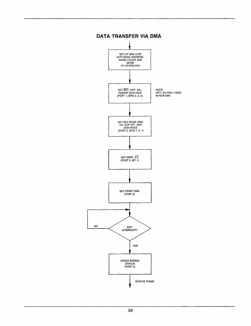
DATA TRANSFER VIA DMA
~ SET-UP DMA CHIP
WITH BASE ADDRESS, WORD COUNT AND
MODE OF OPERATION
I
SET BSY, DIFF. EN., ASSERT DATA BUS
(PORT 1, BITS 5, 3, 0)
,
SET BlK MODE DMA, EN. EOP INT., AND
DMA MODE (PORT 2, BITS 7, 3,1)
SET ASRT. 1/0 (PORT 3, BIT 1)
,~
SET START DMA (PORT 5)
.
NO EOP INTERRUPT?
YES
,I
CHECK ENDING STATUS (PORT 5)
STATUS PHAS ,
39
E
NOTE: DIFF. EN ONLY USED IN NCR 5381.
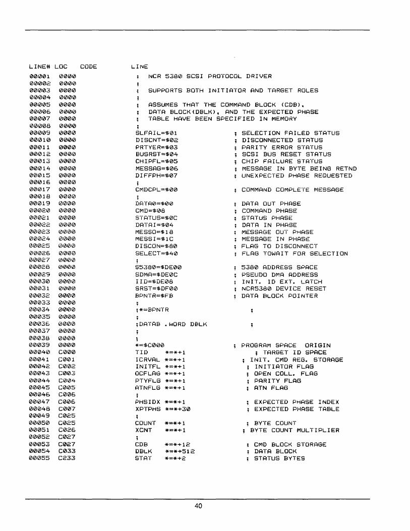
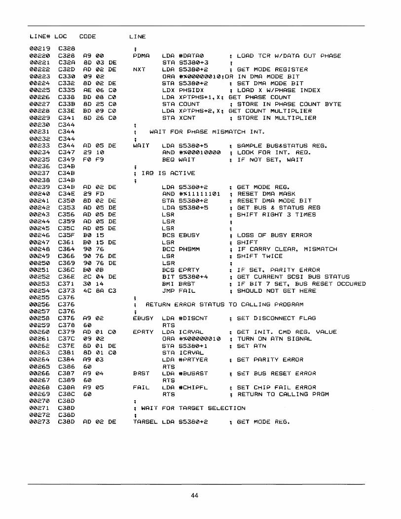
LINE# LOC CODE
00001 0000 00002 121000 1210003 0000 00004 0000 0012105 12101210 00006 012100 0121007 0000 00008 0000 00009 0000 00010 0121121121 0012111 121000 00012 12101210 00013 012100 00014 0000 0121015 0000 00016 001210 00017 121000 0012118 121000 00019 0000 001212121 000121 0121021 001210 1210022 0000 00023 01211210 00024 012101ZI 00025 i() 0 121 121 00026 001210 00027 001210 0012128 001210 0121029 000121 0012130 Q)I2IIZ11Z1 00031 0000 00032 012100 0012133 121000 00034 121000 00035 0000 012112136 001210 0121037 0000 012112138 001210 12112112139 121000 0012140 C01210 00041 C001 1210042 C002 00043 C003 00044 C004 00045 C005 00046 C006 00Q)47 C006 00048 C007 00049 C025 0121050 C025 0121051 C026 00052 C027 012112153 C027 00054 C033 00055 C233
LINE
NCR 5380 SCSI PROTOCOL DRIVER
SUPPORTS BOTH INITIATOR AND TARGET ROLES
ASSUMES THAT THE COMMAND BLOCK (CDB)~
DATA BLOCK(DBLK), AND THE EXPECTED PHASE TABLE HAVE BEEN SPECIFIED IN MEMORY
; SLFAIL=$01 DISCNT=$02 PRTYER=$03 BUSRST=$04 CHIPFL=$05 MESSAG=$06 DIFFPH=$07 ; CI"1DCPL=$00 ; DATA0=$1Z10 CMD=$08 STATUS=$0C DATAI=$04 IYIESSO=$18 MESSI=$lC DISCON=$80 SELECT=$40
85380=$DE00 SDMA=$DEIZtC IID=$DE08 SRST=$DF01Z1 BPNTR=$FB
;*=BPNTR ; ;DATAB .~ORD DBLK
; *=$C0Q.~0
TID *=*+1 ICRVAL *=*+1 INITFL *=*+1 OCFLAG *=*+1 PTYFLG *=*+1 ATNFLG *=*+1 ; PHSIDX *=*+1 XPTPHS *=*+30 ; COUNT *=*+1 XCNT *=*+1 ; CDB *=*+12 DBLK *=*+512 STAT *=*+2
40
SELECTION FAILED STATUS DISCONNECTED STATUS PARITY ERROR STATUS SCSI BUS RESET STATUS CHIP FAILURE STATUS MESSAGE IN BYTe BEING RETND UNEXPECTED PHASE REQUESTED
COMMAND COMPLETE MESSAGE
DATA OUT PHASE COMI'tlAND PHASE STATUS PHASE DATA IN PHASE MESSAGE OUT PHASE MESSAGE IN PHASE FLAG TO DISCONNECT FLAG TOWAIT FOR SELECTION
5380 ADDRESS SPACE PSEUDO DMA ADDRESS INIT. ID EXT. LATCH NCR5380 DEVICE RESET DATA BLOCK POINTER
PROGRAM SPACE ORIGIN ; TARGET 10 SPACE
; INIT. CMD REG. STORAGE INITIATOR FLAG OPEN COLL. FLAG PARITY FLAG ATN FLAG
EXPECTED PHASE INDEX EXPECTED PHASE TABLE
; BYTE COUNT BYTE COUNT MULTIPLIER
CMD BLOCK STORAGE DATA BLOCK STATUS BYTES
LINE*!: LOC CODE LINE
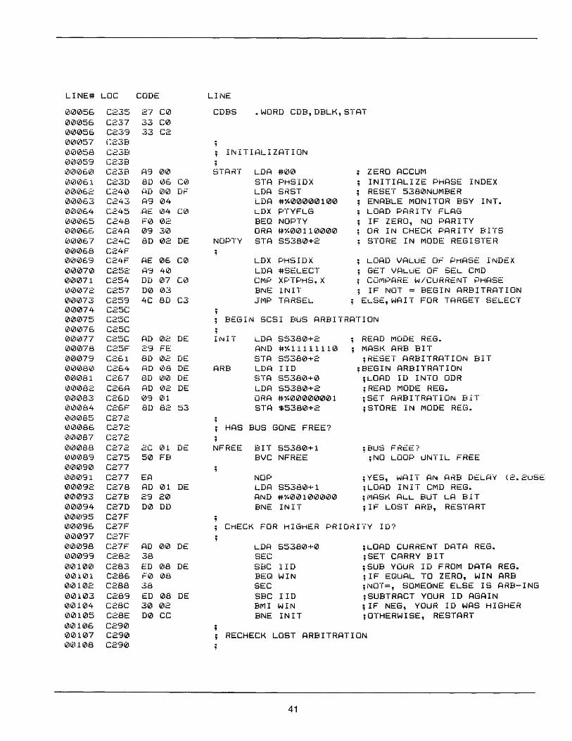
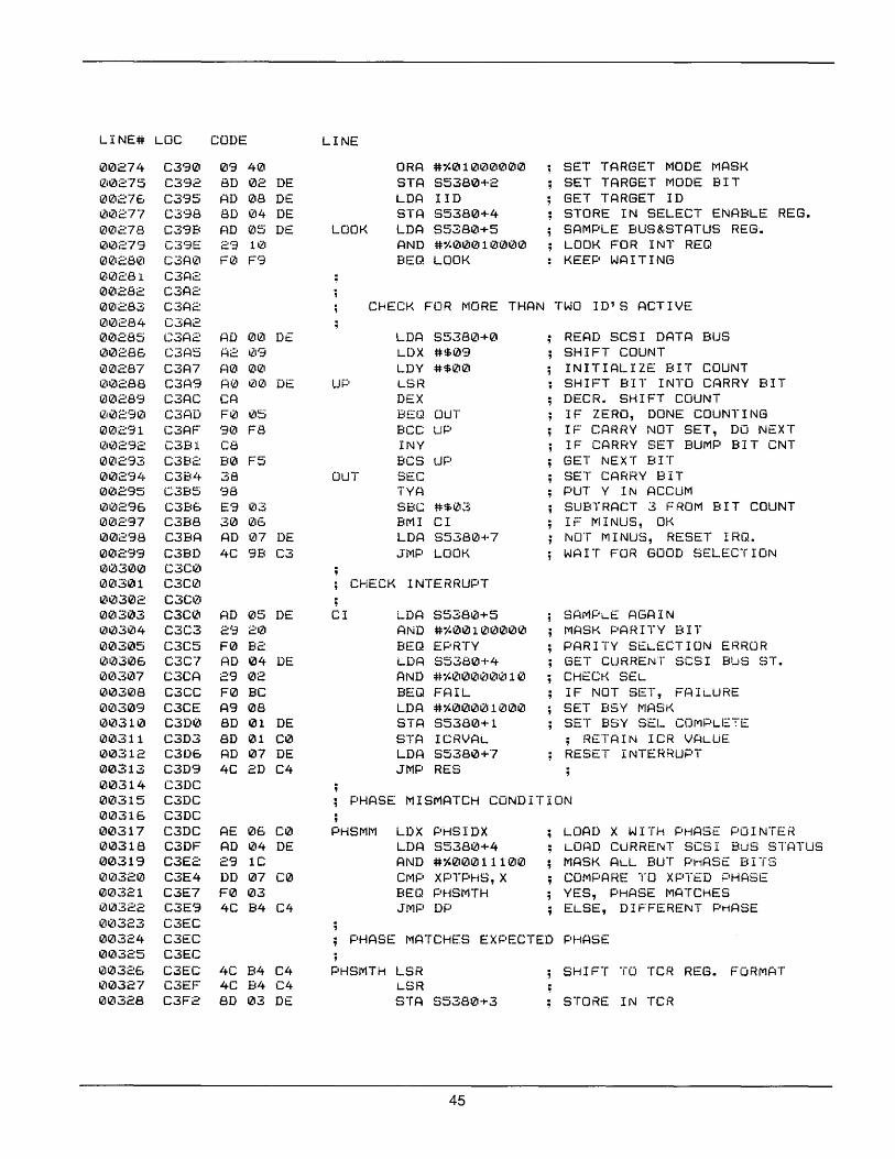
12112112156 C235 27 CIZ1 COBS • WORD CDB,DBLK, STAT 121121056 C237 33 C0 QI012156 C239 33 C2 121012157 1:23B 121 Q) 12158 C238 INITIALIZATION 1l)i{)Q)59 Cc:3B ; 12101216121 C23B A9 121121 START LDA #i{)0 ZERO ACCUM 0121061 C23D 8D 06 eel STA PHSIDX INITIALIZE PHASE INDEX 121012162 CL:::40 AD Q)IL' DF LDA SRST RESET 5380NUMBER 12112112163 C243 A9 04 LDA #1.1211210012111210 ENABLE MONITOR BSY 11\1T. 00064 C245 .AE 04 e0 LDX PTYFLG LOAD PARITY FLAG 0012165 C248 F0 02 BEQ NOPTY IF ZERO, NO PARITY 12112112166 C24A 09 30 ORA #'t.01Z111001Z1121 OR IN CHECK PARITY Brrs QI121067 C24C 8D 02 DE NOPTY STA S538121+2 STORE IN MODE REGISTER 12112112168 C24F 121 QI tZlE. 9 C24F AE 1Z1E. CI21 L_DX PHSIDX LOAD VALlJE: OF PHASE II'-IOEX 0012170 C252 A':;l 4Q.~ LDA #SELECT GET VALJ.JE OF SEI_ ervlo 012112171 C254 DD 1217 C0 CMP XPTPHS,X COIYlPARE w/CURRENT PHASE @ZIQI72 C257 DI2I 121-;;' ..... BNE INI,.. ; IF NOT = BEGIN ARBITRATION o ti) QI 7 3 C259 4C BD C3 JMP TARSEL ; Ei....SE,WAIT FOR TARGET SELECT 121012174 C25C 001Z17~:; C25C BEGIN SCSI BUS ARBITRATION 121012176 C25C ; 0121077 C25C AD 1212 DE INIT LDA S5380+2 READ MODE REG. 1210078 C25F 29 FE AND #1.11111110 MASK ARB BIT 0012179 C2E.l 8D 1212 DE STA S5380+2 ;RE8ET ARBITRATION BIT 0121080 C2EA AD III 8 DE ARB LOA 110 ;BEGIN ARBITRATION 00081 C267 80 0121 DE STA 5538121+0 ;LOAD ID INTO ODR 1210082 C26A AD 02 DE LOA 85380+2 ;READ IVIODE REG. 00083 C26D 09 ell ORA #1.12101210012101 ;SET ARBITRATION BiT 00084 C26F 8D 82 53 STA $538121+2 ;STORE IN MODE REC3. 00085 C272 00086 C272 HAS BUS GONE FREE? 00087 C272 ; 0008£.1 C272 2C 01 Dt:: NFREE BIT 5538121+1 ;BUS FREE ~i iLl tZI 089 C275 50 FB BVC NFREE ;NO LOOP UNTIL FREE 001219121 C277 0121091 C277 EA NOP ; YES, WAIT AN ARB DELAY (2.2USE 00092 C278 AD 01 DE LDA 85380+1 ;LOAD IN!T CIVID REG. 00093 C27B 29 20 AND :fI:~~0010012100 ;I'1ASt{ ALL BUT LA BIT 0121094 C27D DI2I DD BNE INIT ;IF LOST ARB, RESTART 0012195 C27F 00096 C27F CHECK FOR HIGHER PRIORI",Y ID? o tZI 12197 C27F 0121098 Ci.:::7F AD tZI0 DE LDA 85380+0 ;LOAD CURRENT DATA REG. 121121099 C282 38 SEC ;SET CARRY BIT 012110121 C283 ED 1218 DE sac lID ;5UB YOUR ID FROM DATA REG. 00101 C286 FI2I 08 BEQ WIN ;IF EQUAL TO ZERO, WIN ARB 0121102 C288 38 SEC ;I\IOT=, SOMEONE ELSE IS ARB-ING 00103 C289 ED 08 DE SBC lID ;SUBTRACT YOUR ID AGAIN 00104 C28C 3121 02 BI"1I WIN ;IF NEG, YOUR ID WAS HIGHER 121121105 C28E D0 CC BNE INIT ;OTHERWISE, RESTART 0121106 C290 0QI107 C290 RECHECK LOST ARBITRATION 0Q'108 C290
41
LINE# LOC CODE LINE
1211211121'3 C2'30 AD 1211 DE WIN LDA S538121+1 ;LOAD INIT. C\YID REG. 121121110 C293 29 2121 AND #1-1211211121121121121121 ;MASK ALL BUT LA BIT 121121111 C295 DI21 C5 BI\IE INIT ;IF LOST ARB, RESTART 1210112 C297 121121113 C297 A9 I21C LDA #1-121012.101100 ;LOAD VALUE TO SET SEL SIGNAL 121121114 C299 AE 1215 C0 LDX ATNFLG ;LOAD ATN FLAG 121121115 C29C F0 02 BEQ WOATN ; IF ZERO, SEL W/O ATN 0121116 C29E 1219 02 ORA #1-12100001211121 ; OR IN ATN BIT 0121117 C2A0 80 01 DE WOATN STA S538121+1 ;TURN ON SEL LINE 121121118 C2A3 00119 C2A3 WAIT 1.2 USEe 121121120 C2A3 12112112l. C2A3 EA NOP 0121122 C2A4 AD 1212 CI21 LOA INITFL ;LOAD IN A SOFTWARE FLAG 1210123 C2A7 00 0D BNE SEL ;IF FLAG SET, PERFORM INIT. BEL 1210124 C2A'3 1210125 C2A9 ELSE, TARGET RESELECTION 00126 C2A9 00127 C2A9 1210128 C2A9 AD 02 DE LDA S538121+2 ;READ IVIODE REG. 121012';) C2AC 1219 40 ORA #1-12111210121000 ; ENABLE TARGET MODE 012113121 C2AE SD 1212 DE STA S538121+2 ;SET TARGET MODE 00131 C2B1 A'3 1211 LDA #$1211 ;ENABLE ASSERT liD 121121132 C2B3 80 03 DE STA 8538121+3 ;SET ASSERT I/O 00133 C2B6 ; 121121134 C2B6 AD 1218 DE 8EL LOA 110 ; LOAD INITIATOR 10 121121135 C2B9 1210 121121 C0 ORA TID ; OR IN TARGET ID 121121136 C2BC BD 121121 DE STA 8538121+121 ;LOAD INT & TAR 10'8 INTO OOR 1210137 C2BF 121121138 C2BF TEST FOR DIFFERENTIAL PAIR 0121139 C2BF 1210140 C2BF A9 1215 LOA #1-121012112112111211 ;8EL & DATA BUS BITS 1210141 C2C1 AE 03 CI21 LDX OCFLAG ;LOAD IN A SOFTWARE FLAG 121121142 C2C4 0121 02 BNE OPNCOL ;IF FLAG SET, OPEN COLLECTOR 1210143 C2C6 121121144 C2C6 DIFFERENTIAL PAIR 121121145 C2C6 0121146 C2C6 09 2121 ORA #1-0121101210121121 . OR IN DIFF. ENBL BITS .. 0121147 C2C8 80 1211 DE OPNCOL STA S5380+1 ;SET SEL, DATA BUS, & (DIFF. PAl 1210148 C2CB 80 1211 C0 8TA ICRVAL ; RETAIN VALUE OF INIT CMD REG. 12112114'3 C2CE 0015121 C2CE RESET ARBITRATION BIT 121121151 C2CE 00152 C2CE AD 02 DE LDA S538121+2 ;REAO MODE REGISTER 00153 C2Dl 29 FE AND #Y-1111111121 ;MA8K ARB BIT 00154 C2D3 80 02 DE 8TA 85380+2 ;RE8ET ARB BIT 00155 C2D6 ; 0121156 C2D6 DI8ABLE THE 8EL EN REGISTER TO AVOID A 8EL INT. 1210157 C2D6 00158 C2D6 A9 0121 LDA #$0121 ZERO ACCUM. 1210159 C2D8 8D 04 DE STA S5380+4 ZERO SELECT ENABLE REG. 0016121 C2DB 00161 C2DB RELEASE BUSY 121121162 C2DB 00163 C2DB AD 1211 CI2I LDA ICRVAL GET INIT CMD REG VALUE
42
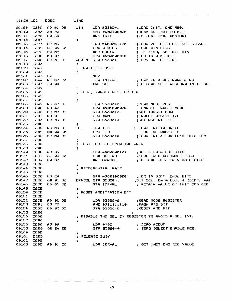
LINE# LOC
00164 00165 00166 00167 00168 00169 00170 00171 00172 00173 0121174 00175 00176 0121177 00178 00179 00180 1210181 00182 00183 00184 00185 00186 00187 00188 00189 00190 00191 00192 00193 00194 00195 00196 00197 00198 00199 00200 00201 00202 01Z1203 00204 00205 00206 00207 00208 00209 0021121 00211 00212 00213 00214 00215 00216 00217 00218
C2DE C2E0 C2E3 C2E6 C2E6 C2E6 C2E6 C2E8 C2EA C2ED C2EF C2EF C2EF C2EF C2F0 C2F2 C2F3 C2F5 C2F5 C2F5 C2F5 C2F7 C2FA C2FC C2FF C301 C302 C304 C304 C304 C304 C306 C307 C307 C307 C307 C30A C30D C30F C311 C314 C317 C319 C31C C31F C322 C322 C322 C322 C323 C325 C328 C328 C328 C328
CODE
29 F7 80 01 DE 80 01 C0
A0 60 A2 FF 2C 04 DE 70 18
CA D0 F8 88 D0 F3
A9 00 80 00 DE A2 20 2C 04 DE 70 06 CA D0 F8
A9 01 60
AD 01 C0 AE 02 C0 D0 08 09 08 8D 01 DE 80 01 C0 A9 28 2D 01 C0 8D 01 DE 80 01 C0
CA F0 03 4C 20 C4
LINE
AND #~11110111 STA S5380+1 STA ICRVAL
MASK OUT BSY BIT RESET BSY RETAIN ICR VALUE
NOW WAIT 400NSEC AND BEGIN LOOKING FOR BSY
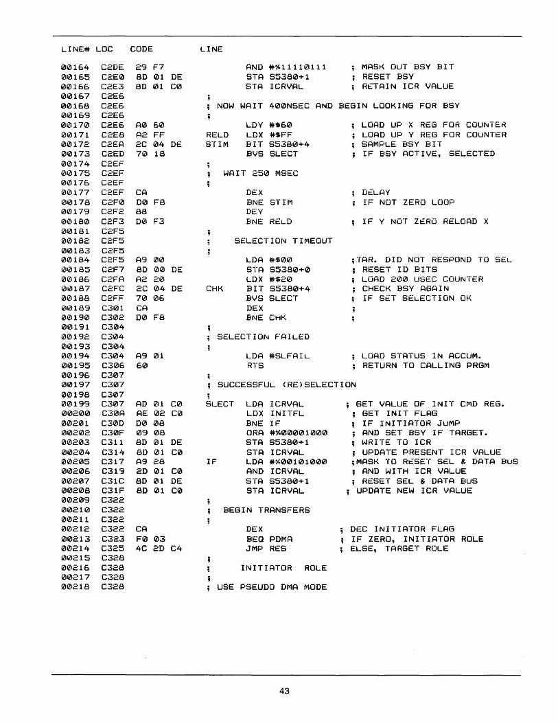
RELD STIM
LDY #$60 LOX #$FF BIT S5380+4 BVS SLEeT
WAIT 250 MSEC
CHK
DEX BNE STIM DEY BNE RELD
SELECTION TIMEOUT
LOA #$00 8TA 85380+0 LDX #$20 BIT 85380+4 evs SLECT DEX BNE CHK
SELECTION FAILED
LDA #SLFAIL RTS
LOAD UP X REG FOR COUNTER LOAD UP Y REG FOR COUNTER SAMPLE BSY BIT IF BSY ACTIVE, SELECTED
Dt::LAY IF NOT ZERO LOOP
IF Y NOT ZERO RELOAD X
;TAR. DID NOT RESPOND TO SEL RESET ID BITS LOAD 200 USEC COUNTER CHECK BSY AGAIN IF SET SELECTION OK
LOAD STATUS IN ACCUM. RETURN TO CALLING PRGM
SUCCESSFUL (RE)SELECTION ; SLECT LDA ICRVAL
LDX INITFL BNE IF ORA #"00001000 STA 85380+1 STA ICRVAL
IF LDA *"00101000 AND ICRVAL STA 85380+1 8TA ICRVAL
BEGIN TRAN8FERS
DEX BEQ PDMA JMP RES
INITIATOR ROLE
U8E PSEUDO DMA MODE
43
; GET VALUE OF INIT CMD REG. GET INIT FLAG IF INITIATOR JUMP AND SET BSY IF TARGET. WRITE TO ICR
; UPDATE PRESENT ICR VALUE ;MASK TO RESET SEL & DATA BUS ; AND WITH ICR VALUE ; RESET BEL & DATA BUS
; UPDATE NEW ICR VALUE
DEC INITIATOR FLAG IF ZERO, INITIATOR ROLE ELSE, TARGET ROLE
LINE# LOC
1210219 1210220 0121221 121121222 121121223 121121224 0121225 121121226 121121227 121121228 00229 12112123121 121121231
C328 C328 C32A C32D C330 C332 C335 C338 C33B C33E C341 C344 C344
121121232 C344
CODE
A9 121121 8D 03 DE AD 1212 DE 1219 1212 8D 1212 DE AE 06 CI2I BD 1218 CI2I 8D 25 Ct2I BD 1219 CI2I 8D 26 CI2I
0121233 C344 AD 1215 DE 121121234 C347 29 1121 121121235 C349 FI2I F9 1210236 C34B 121121237 C34B 121121238 C34B 1210239 12112124121 121121241 0121242 121121243 0121244 121121245 1210246 121121247 00248 121121249 0121250 121121251 0121252 121121253 121121254 1210255 121121256 121121257 121121258 0121259 121121260 00261 121121262 121121263 0121264 121121265 1210266 1210267 121121268 121121269 121121270 121121271 1210272 0121273
C34B C34E C35121 C353 C356 C359 C35C C35F C361 C364 C366 C369 C36C C36E C371 C373 C376 C376 C376 C376 C378 C379 C37C C37E C381 C384 C386 C387 C389 C38A C38C C38D C38D C38D C38D
AD 1212 DE 29 FD 8D 1212 DE AD 1215 DE AD 1215 DE AD 05 DE AD 1215 DE B0 15 BI2I 15 DE 9121 76 9121 76 DE 90 76 DE BI2I I2IB 2C 1214 DE 3121 14 4C 8A C3
A9 1212 60 AD 1211 C0 1219 1212 8D 1211 DE 8D 01 C0 A9 1213 6121 A9 04 6121 A9 05 6121
AD 02 DE
LINE
; PDMA
NXT
; WAIT
LOA #OATAI2I STA S538121+3
LOAD TCR W/DATA OUT PHASE
LOA S5380+2 GET MODE REGISTER ORA ~~012100012110;OR IN DMA MODE BIT STA S538121+2 seT DMA MODE BIT LOX PHSIDX ; LOAD X W/PHASE INDEX LDA XPTPHS+1,X; GET PHASE COUNT STA COUNT ; STORE IN PHASE COUNT BYTE LDA XPTPHS+2,X; GET COUNT MULTIPLIER STA XCNT ~ STORE IN MULTIPLIER
WAIT FOR PHASE MISMATCH INT.
LDA S5380+5 AND ~1.12I121121101211210
BEQ WAIT
SAMPLE BUS&STATUS REG. LOOK FOR INT. REQ. IF NOT SET, WAIT
IRQ IS ACTIVE
LDA S5380+2 AND #1.1111111211 STA S538121+2 LOA S538121+5 LSR LSR LSR BCS EBUSY LSR BCC PHSMM LSR LSR BCS EPRTY BIT S538121+4 BMI BRST JMP FAIL
GET MODE REG. RESET DMA MASK RESET DMA MODE BIT GET BUS & STATUS REG SHIFT RIGHT 3 TIMES
LOSS OF BUSY ERROR SHIFT IF CARRY CLEAR, MISMATCH SHIFT TWICE
IF SET. PARITY ERROR GET CURRENT SCSI BUS STATUS IF BIT 7 SET, BUS RESET OCCURED SHOULD NOT GET HERE
RETURN ERROR STATUS TO CALLING PROGRAM ; eBUSY LDA #DISCNT
RTS EPRTY LDA ICRVAL
BRST
FAIL
ORA ~1.012112101211211121
STA S5380+1 STA ICRVAL LDA #':'RTYER RTS LOA "BUSRST RTS LDA #CHIPFL RTS
SET DISCONNECT FLAG
GET INIT. CMD REG. VALUE TURN ON ATN SIGNAL S'::T ATN
SET PARITY ERROR
S'::T BUS RESET ERROR
SET CHIP FAIL ERROR RETURN TO CALLING PRGM
WAIT FOR TARGET SELECTION ; TARSEL LOA S5380+2 ; GET MODE REG.
44
LINE# LOC CODE LINE
00274 C390 09 40 ORA #~01000000 SET TARGET MODE MASK Q)0275 C392 8D 02 DE STA S5380+2 SET TARGET MODE BIT 00275 C395 AD 08 DE LOA 110 GET TARGET 10 1210277 C398 80 04 DE STA S5380+4 STORE IN SELECT ENABLE REG. 1210278 C39B f:.)0 05 DE LOOK LOA S538121+5 SAMPLE BUS&STATUS REG. 00279 C39E 29 1121 AND #~~00010000 LOOK FOR INT REQ 12112128121 C3A1l' FI21 F9 BEQ LOOK KEEP WAITING 00281 C3A2 1210282 C3A2 0121283 C3A2 CHECK FOR MORE THAN TWO IO'S ACTIVE 121121284 C3A2 1210285 C3A2 AD 00 DE LDA 85380+0 READ SCSI DATA BUS 00285 C3A5 A2 09 LDX #$09 SHIFT COUNT 1210287 C3A7 A0 00 LDY #$00 INITIALIZE BIT COUNT 1210288 C3A9 AIZ! 00 DE UP LSR SHIFT BIT INTO CARRY BIT 00289 C3AC CA DEX DECR. SHIFT COUNT 1210290 C3AD F0 III 5 BEQ OUT IF ZERO, DONE COUNTING 002'31 C3AF 9121 F8 BCC UP IF CARRY NOT SET, DO NEXT IZlIi)292 C3Bl C8 INY IF CARF<Y SET BUMP BIT CNT 01212'33 C3B2 B0 F5 BCS UP GET NEXT BIT 012129L~ C3B4 38 OUT 8EC SET CARRY BIT 002'35 C3B5 98 TVA PUT Y IN ACCUM 00295 C3B6 E9 03 SBC #$1ZI3 SUBTRACT ~ I::'-ROM BIT COUNT 00297 C3B8 30 06 BMI CI IF IVIINUS, OK 0121298 C3BA AD 1217 DE LDA S5380+7 !\lOT MINUS, RESET IRQ. 00299 C3BD 4C 9B C3 JOMP LOOK WAIT FOR GOOD SELECTION 0030121 C3C0 00301 C3C0 CHECK INTERRUPT 0121302 C3C0 00303 C3C0 AO 05 DE CI LDA S5380+5 SAMP .... E AGAIN 0031214 C3C3 29 20 AND #'1-00100000 MASK PARITY BIT 00305 C3C5 F0 B2 BEQ EPRTY PARITY SELECTION ERROR 0121306 C3C7 AD 04 DE LDA 85380+4 GET CURRENT SCSI BUS ST. 0121307 C3CA 29 1212 AND :j:/:~00IZ1eIlZI010 CHEC~{ SEL 00308 C3CC F0 BC BEQ FAIL IF NOT SET, FA I I...URE 00309 C3CE A9 08 LOA #~000121101210 SET BS\( MASK 00310 C3D0 80 01 DE STA S538121+1 SET BSY BEL COMPLE:E 00311 C3D3 BD 01 C0 STA ICRVAL , RETAIN ICR VALUE 00312 C3D6 AD 07 DE LOA S5380+7 RESET INTERRUPT 00313 C3D9 4C 20 C4 JMP RES 0121314 C30C 00315 C30C PHASE MISMATCH CONDITION 00315 C3DC 00317 C30C AE 06 C0 PHSMM LDX PH8IDX LOAD X WITH PHASE POINTEt~
00318 C3DF AD 04 DE LOA 85380+4 LOAD CURREI\IT SCSI BuS STATUS 00319 C3E2 29 1C AND #~1ZI0011100 MASK AI...L BUT PHASE BI-CS 0121320 C3E4 DO 07 C0 CMP XPTPHS,X COMPARE TO XPTED PHASE 00321 C3E7 F0 03 SEQ PH8MTH YES, PHASE MATCHES 121121322 C3E9 4C B4 C4 JMP DP ELSE, DIFFERENT Pt-1A8E 00323 C3EC 00324 C3EC PHASE MATCHES EXPECTED PHASE 00325 C3EC 00326 C3EC 4C B4 C4 PHSMTH LSR SHIFT TO TCR REG. FORMAT 1Z10327 C3EF 4C 84 C4 LSR 0032B C3F2 80 03 DE STA 85380+3 STORE IN TCt<
45
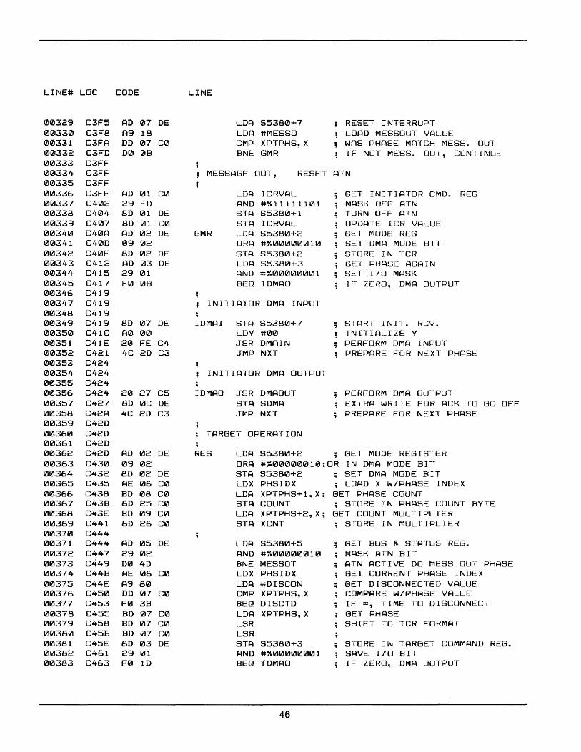
LINE# LOC CODE LINE
00329 C3F5 AD 07 DE LDA 55380+7 RESET INTERRUPT 00330 C3F8 A9 18 LDA #IYIESSO LOAD IYIESSOUT VALUE 00331 C3FA DD 07 C0 CMP XPTPHS, X WAS PHASE MATCM MESS. OUT 00332 C3FO 00 I2IB BNE GMR IF NOT MESS. OUT, CONTINUE 121121333 C3FF 00334 C3FF MESSAGE OUT, RESET ATN 00335 C3FF 00336 C3FF AD 01 C0 LDA ICRVAL GET INITIATOR CMD. REG 00337 C402 29 FD AND #'Y-llll111211 MASK OFF ATN 00338 C41214 80 01 DE STA 85380+1 TURN OFF ATN 00339 C407 8D 1211 C0 STA ICRVAL UPDATE ICR VALUE 00340 C40A AD 02 DE: GMR LDA 55380+2 GET fYlODE REG 00341 C40D 09 02 ORA #'Y-00000010 SET DMA MODE BIT 00342 C40F 8D 02 DE STA S538121+2 STORE IN TCR 00343 C412 AD 03 DE LDA S538121+3 GET PHASE AG~=lIN
00344 C415 29 01 AND #'Y-00000001 SET I/O MASK 00345 C417 F0 0B BEQ IDMAO IF ZEI10, DMA OUTPUT 00346 C419 00347 C419 INITIATOR DMA INPUT 00348 C419 ; 00349 C419 8D 07 DE IDMAI STA S5380+7 START INIT. Rev. 00350 C41C A0 00 LOY #00 INITIALIZE Y 00351 C41E 20 FE C4 JSR DMAIN PERFORf'I1 DI't1A INPUT 00352 C421 4C 2D C3 JMP NXT PREPARE FOR NEXT PH?~SE
00353 C424 00354 C424 INITIATOR DMA OUTPUT 00355 C424 ; 00356 C424 20 27 C5 IDMAO JSR DIYIAOUT PERFORM DIYIA OUTPUT 00357 C42"' 80 0C DE STA SOMA EXTRA WRITE FOR ACK TO GO OFF 00358 C42A 4C 2D C3 JMP NXT PREPARE FOR NEXT PHASE 00359 C420 00360 C42D TARGET OPERATION 00361 C420 ; 00362 C42D AD 02 DE RES LDA S5380+2 ; GET MODE REGISTER 00363 C430 09 02 ORA *'Y-00000010;OR IN DIYIA MODE BIT 00364 C432 8D 02 DE STA S5380+2 SET DMA MODE BIT 00365 C435 AE 06 C0 LDX PHSIOX LOAD X W/PHASE INDEX 00366 C438 BD 08 C0 LDA XPTPHS+l, X; GET PHASE COUNT 00367 C43B 8D 25 C0 STA COUNT ; STORE IN PHASE COUNT BYTE 00368 C43E BO 09 C0 LDA XPTPHS+2,X; GET COUNT MULTIPLIER 00369 C441 8D 26 C0 STA XCNT STORE IN MULTIPLIER 00370 C444 00371 C444 AD 05 DE LDA S5380+5 GET BUS & STATUS REG. 00372 C447 29 02 AND #'Y-00000010 MASI-< ATN BIT 00373 C449 00 4D BNE MESSOT ATN ACTIVE DO MESS OUT PHASE 00374 C44B AE 06 C0 LOX PHSIDX GET CURRENT PHASE INDEX 00375 C44E A9 80 LOA #DISCON GET DISCONNECTED VALUE 00376 C450 OD 07 C0 CMP XPTPHS, X COMPARE W/PHASE VALUE 00377 C453 F0 3S BEQ OISCTO IF =, TIME TO 0 I SCONNEC"j 00378 C455 SD 07 C0 LOA XPTPHS,X GET PHASE 00379 C458 SD 07 C0 LSR SHIFT TO TCR FORMAT 00380 C45B BD 07 C0 LSR 00381 C45E 8D 03 DE STA 55380+3 STORE IN TARGET COMMAND REG. 00382 C461 29 01 AND #~00000001 SAVE liD BIT 00383 C463 F0 10 BEQ TDMAO IF ZERO, DMA OUTPUT
46
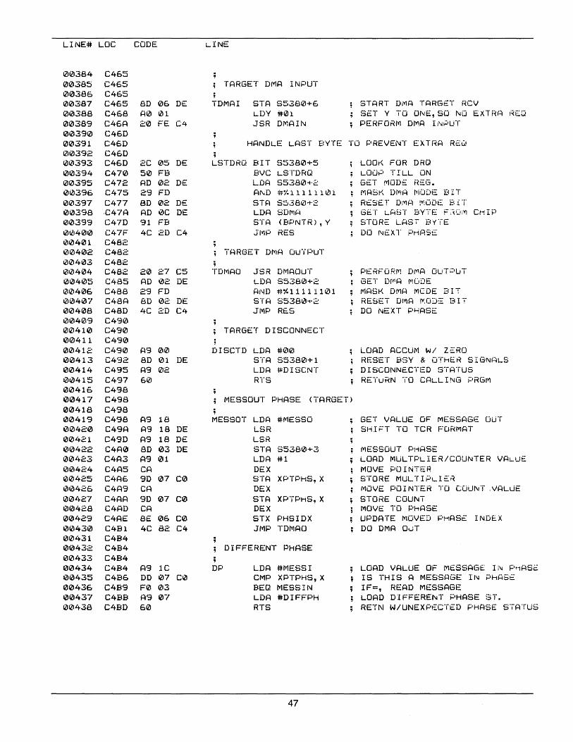
LINE# LOC CODE LINE
00384 C465 00385 C465 TARGET DMA INPUT 00386 C465 00387 C465 80 06 DE TDMAI STA S5380+6 START DlvtA TARGET f~CV
121121388 C468 A0 1£'1 LDY #1£'1 St::T Y TO Of\!E,SD NO EXTF«.::'! I~EQ
00389 C46A 20 FE C4 JSR DMAIN PERFORI"1 DMA IN~IUT
00390 C46D 00391 C46D HANDLE LAST BYTr:: TO PREVENT EXTRA ReC! 121121392 C46D ; 00393 C46D 2C 05 DE LSTDRG! BIT 85380+5 LOOt{ FOR DRQ 00394 C47121 5121 FB Bve L8TDRQ LOO~I TILL ON 00395 C472 AD 02 DE LDA S5380+2 GET MODE HSG. 00396 C475 29 FD AND 41=1.1 1 1 1 1 101 MASK DiYlH ""iDDE BIT 003'37 C477 80 02 DE STA 8:5380+2 RESET Di'1?-) !Y\ODt.=~ Be:' 00398 ·C47A AD 0C DE LDA SDIYIH GET LAbT BYTE F :( CI;'1 C~"'!IP
1210399 C47D 91 FB STA (BPNTR),Y STORE L.AST By'-~"E
01lt400 C47F 4C 2D C4 J'ITlP RES DO NI:::XT Pt-j/~SE
1210401 C482 00402 C482 TARGET DIY/A DU-fPUT 00403 C482 ; I2Itll404 C482 20 27 C5 TDMAO JSR DMAOUT PERFO.RM DIYlA Ou'T'::'LJT 00405 C485 AD 02 DE LDA 85380-1-2 GET DffiA ,..l(JDE 121041216 C48a 29 FD AND *~1.1 1111 101 MASK DMA MGDE BIT 00407 C48A aD 02 DE 8TA S5381l1-t-2 RESET o 1"1 A fY.OD:=: BIT 00408 C480 4C 2D C4 JMP RE.S DO NEXT PI-lAS:::: 00409 C490 1210410 C490 TARGET DISCONNECT 00411 C4'30 00412 C490 A9 00 DISCTD LDA #00 LOAD ACCUM WI Z~RO
00413 C492 8D 01 DE S'rA 5538121+1 RESET Bf:3Y & CiTI-1ER SI GNf~~LS 00414 C495 A9 02 LDA #DISCNT DISCONNECTED STATUS 00415 C497 6121 RTS REYuRN ~tO CALLING PRGM 00416 C49a 00417 C49a MESSOUT PHASE (TARGET) 00418 C498 00419 C498 A9 18 MESSOT LDA #MESSO GET VALUE OF MESSAGE (JUT 1210420 C49A A9 18 DE LSR SHIFT TO TCR FORIYIAT
00421 C490 A9 18 DE LSR 00422 C4A0 80 03 DE STA 8538121+3 fYlESSOUT PHASE 00423 C4A3 A9 01 LDA #1 LOAD MULTPLIER/COUNTER VA!....UE 00424 C4A5 CA DEX MOVE POINTER 00425 C4A6 90 07 C0 STA XPTPHS,X STORE MULT I ~'L I i:>< 00426 C4A9 CA DEX MOVE POINTER TO CQUI\IT .VALLiE 00 L,,2-' C4AA 90 07 C0 STA XPTPHS, X STORE COUNT 00428 C4AD CA DEX MOVE TO Pl-1ASE 00429 C4AE 8E 06 C0 STX PHSIDX UPDATE ~10VED PH~~St::: INDE.X 00430 C4Bl 4C 82 C4 JMP TDMAO DO DMA OwT 00431 C4B4 00432 C4B4 DIFFERENT PHASE 00433 C4B4 ; 00434 C4B4 A9 1C DP LDA #MESSI LOAD VALUE OF Mt::SSAGE Ii'\I Pt1ASC: 00435 C4B6 DD 07 Cill CMP XPTPHS, X IS THIS A MESSAGE IN ;::'hASt:: 00436 C4B9 F0 1213 BEQ MESSIN IF=, READ MESSAGE 0043-' C4BB A9 07 LDA #DIFFPH LOAD DIFFERENT PHASE ST. 00438 C4BO 60 RTS RETI\I W/UNEXPECTED PHASE S-,ATU5
47
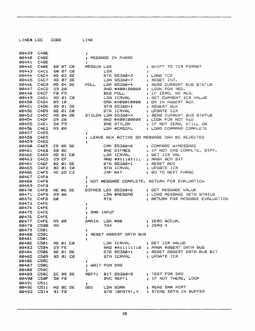
LINE# LOC CODE LINE
1210439 C4BE 0044121 C4BE MESSAGE IN PHASE 00441 C4BE 00442 C4BE 60 07 C0 MESSIN LSR St-HFT TO TCR FORMAT 1210443 C4Cl 60 1217 C0 LSR 00444 C4C4 8D 1213 DE STA S5380+3 LOAD TCR 1210445 C4C7 AD 1217 DE LDA S5380+7 RESET H-.iT. 0121446 C4CA AD 04 DE POLL LDA S5380+4 READ CURRENT BUS STATUS 1210447 C4CD 2'3 2121 AND #~00100IZJ00 LOOK FOR liEG!. 0121448 C4CF F0 F9 BEQ POLL IF ZERO, NO REQ. 0121449 C4Dl AD 01 C0 LDA ICRVAL GET CUrH~ENT ICR V(-)LUE 00450 C4D4 1219 1121 ORA #1.12100112112100 OR IN ASSERT ACK 00451 C4D6 8D 01 DE STA S5380+1 ASSERT ACK 00452 C4D9 80 01 C0 STA ICRVAL UPDATE ICR 1210453 C4DC AD 1214 DE STILON LDA 85380+4 READ CUHRENT BLJ~3 STATUS 0121454 C4DF 29 2121 AND #1.0011210000 LOOK FOR NOT f<EG! 00455 C4El DI2I F9 BNE STILON IF NOT ZERO, STILL ON 0121456 C4E3 A9 1210 LDA #CIYlDCPL LOAD COMMAND COMPLETE 121121457 C4E5 121121458 C4E5 LEAVE ACK ACTIVE SO IYIE8SAGE CAN BE REJECTED 0121459 C4E5 00460 C4E5 CD 06 DE CMP 85380+6 COMPARE W/MESSAGf~
00461 C4E8 D0 0E BNE DIFMES IF NOT CI'r1D COIYIPLTE, DIFf- • 00462 C4EA AD 01 C0 LDA ICRVAL GET ICR VAL 1210463 C4ED 29 EF AND #1.11101111 I",A8K ACt-< BIT 00464 C4EF 80 01 DE STA 85380+1 RESET AC~<
1210465 C4F2 8D 1211 C0 STA ICRVAL UPDATE ICR 0121466 C4F5 4C 2D C3 JMP NXT GO TO NEXT PHASE 0121467 C4F8 1210468 C4F8 NOT MESSAGE COMPLETE, f~ETURN FOR EVALUAT r GI\l
1210469 C4F8 ; 0121470 C4F8 AE 06 DE DIFMES LDX 8538121+6 GET MESSAGE VALUE 1210471 C4FB A9 1216 LDA #IYlE8SAG LOAD MESSAGE RETN STATUS 121121472 C4FD 60 RTS RETURN FOR IVIESSAGE EVALUATION 121121473 C4FE 0121474 C4FE 1210475 C4FE DMA INPUT 00476 C4FE ; 0121477 C4FE A9 121121 DMAIN LOA #121121 ZERO ACCUM. 00478 C500 AA TAX ZERO X 0121479 C501 0048121 C501 RESET ASSERT DATA BUS 121121481 C51211 0121482 C501 AD 01 C0 LOA ICRVAL GET ICR VALUE 00483 C51214 29 FE AND #1.1111111121 MASK ASSERT DAT~~ BUS 0121484 C506 80 1211 DE STA S5381Z1+1 RESET ASSERT DATA BUS BIT 121121485 C51219 80 1211 CIlI STA IeRV(~L UPDATE ICR 1210486 C5IZJC 1210487 C5IZJC WAIT FOR DRQ 00488 C50C ; 121121489 C50C 2C 1215 DE REPT1 BIT S538IZJ+5 TEST FOR DRQ 121049121 C50F 50 FB Bve REPTl IF NOT THERE, LOOP 1210491 C511 ; 121121492 C511 AD IZIC DE Gol LDA SDMA READ DMA PORT 00493 C514 91 FB STA (BPNTR),Y STORE DATr:.~ IN BUFFER
48
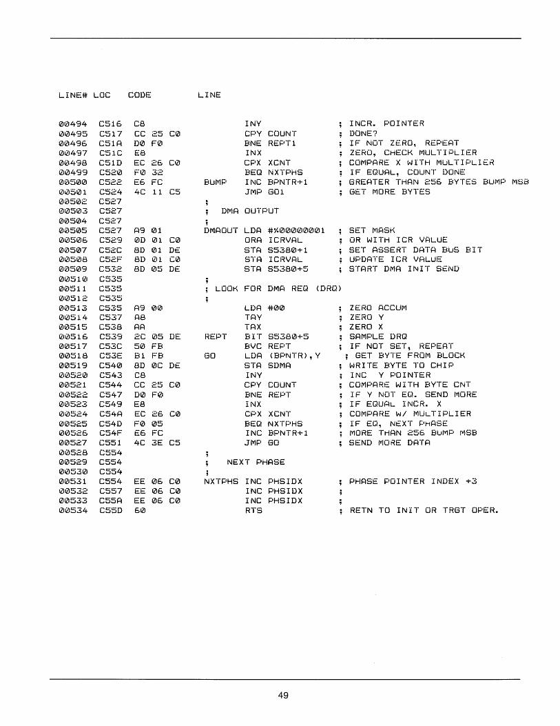
LINE# LOC CODE LINE
1Z11Z1494 C516 C8 INY INCR. POINTER 00495 C517 CC 25 CIZI CPY COUNT DONE'? 1Z10496 C51A D0 F0 BNE REPT1 IF NOT ZE.RO, REPEAT 0tZI497 C51C E8 INX ZERO, CHECK MULTIPLIER 00498 C51D EC 26 C0 CPX XCNT COMPARE X WITH MULTIPLIER 00499 C520 Fill 32 BEQ NXTPHS IF EG1UAL, COUNT DONE 01Z1500 C522 E6 FC BUMP INC BPNTR+1 GREATER THAN 256 BYTES BUIYlP MSB 00501 C524 4C 11 C5 JMP GOl GET MOHE BYTES 01Z1502 C527 1210503 C527 DIVIA OUTPUT 00504 C527 ; 00505 C527 A9 01 DIYIAOUT LDA #r.01Zl0Q.~0001 SET MAS~{
0121506 C529 0D 01 CIZI ORA ICRVAL OR WITH ICR VALUE 00507 C52C 80 01 DE: STA S5380+1 SET ASSERT D~lTA BUS BIT 1210508 C52F 80 01 C0 STA ICRVAL UPDATE ICR VALUE 0121509 C532 80 05 DE STA S5380+5 START DMA INIT SEND 0t2J51tZl C535 01Z1511 C535 LOOK FOR DIYlA REQ (DRQ) 00512 C535 00513 C535 A9 00 LDA #00 ZERO ACCUM 00514 C537 A8 TAY ZERO Y 00515 C538 AA TAX ZERO X tZlt2J516 C539 2C 05 DE REPT BIT 85380+5 SAMPLE DRQ 00517 C53C 50 FB BVC REPT IF NOT SET, f<EPEAT 00518 C53E 81 FB GO LDA (BPNTR),Y ; GET BYTE FROM BLOCK 00519 C540 8D !lIC DE: STA SDMA WRITE BYTE TO CHIP 012152121 C543 C8 INY INC Y POINTER 0121521 C544 CC 25 C0 CPY COUNT COMPARE WITH BYTE CNT 00522 C547 D0 Fill BNE REPT IF Y NOT EC,1. SEND MORE 01Z1523 C549 E8 INX IF EQUAL INCR. X 00524 C54A EC 25 CIlI CPX XCNT COMPAF<E WI IYiULTIPLIER 00525 C54D F0 05 BEQ NXTPHS IF EQ, NE:XT PHASE 00525 C54F E6 FC INC BPNTR+1 MORE THAN 255 BUMP f'18B 00527 C551 4C 3E C5 JMP GO SEND MORE DATA 121121528 C554 0121529 C554 NEXT PHASE 00530 C55'+ ; 01Z1=i31 C554 EE 1216 C0 NXTPHS INC PHSIDX PHASE POINTER INDEX +3 00532 C557 EE 05 CIlI INC PHSIDX 00533 C55A EE 06 C0 INC PHSIDX 00534 C55D 5121 RTS RETN TO INIT OR TRGT OPER.
49
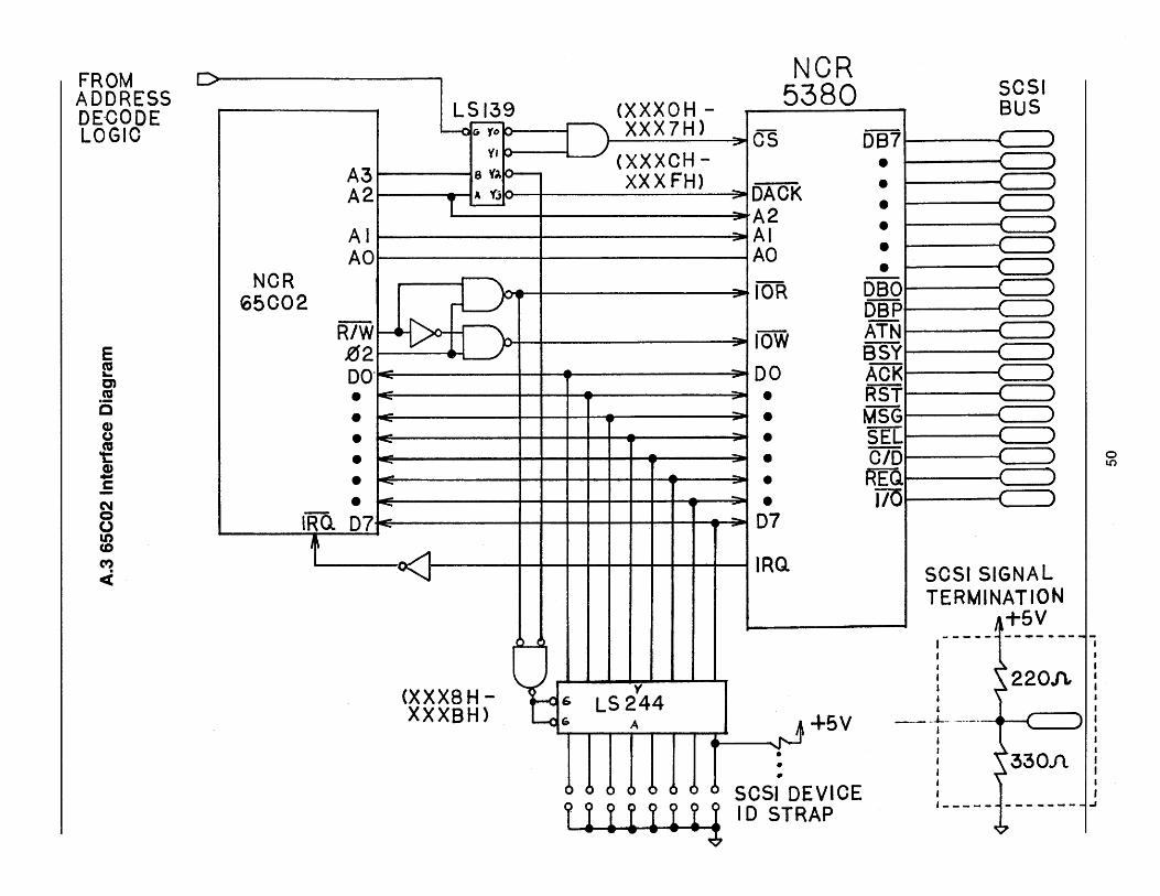
FROM ADDRESS DE-CODE LOGIO
NCR ~5002
IRQ.
t
A3 A2
AI AO
R/W i12 DO-• • • • • • D7
LSI39 r---
'---Cl G yo p vdo
8 VA P-" 1,,10 T l-
,-
H4)o-t-rP ----------------
(XXX8H -XXXBH)
NCR (XXXDH - 5380
1 XXX7H) CS ......, (XXXCH -XXX FH) DAOK -~
.. A2 --- AI ~-
AD
- lOR ---
lOW ----- DO ... .. • --- • -... • -- • - • ---- • - D7 --
IRQ
y
LS244 A +5V
i • •
I) C) C) C ) 4) ()« () SCSI DEVIOE r I I I I I ~ 110 STRAP
SCSI BUS
087 , ) "'
• r ) """-
• r ) ,
• I ) "
• ~ ) r 1 • \.
• \. )
DBO I ) \.
DBP r ) \.
ATN I ) \.
BSY r ) \.
AOK I ) "
RST , 1 ,
MSG r ) \.
SEL r 1 , OlD r ) -,.
REQ r ) , i/O r ) \.
5051 SIGNAL TERMINATIO N
,a+5V 1------ -.. ~- -I
• ~220 I I , ~ ,
____ ~.~J-..- .----- r ""\.
I I I ~330 I I , I
f\. , 1 ____________ .J
o LO
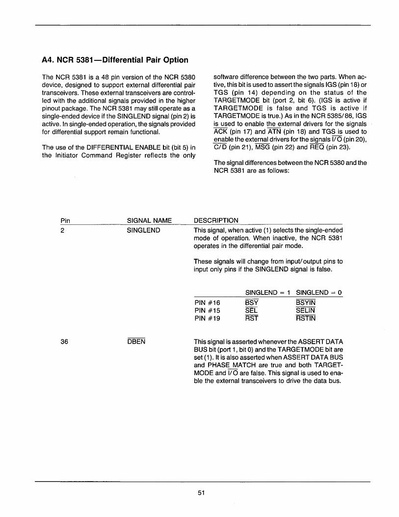
A4. NCR 5381-Differential Pair Option
The NCR 5381 is a 48 pin version of the NCR 5380 device, designed to support external differential pair transceivers. These external transceivers are controlled with the additional signals provided in the higher pinout package. The NCR 5381 may still operate as a single-ended device if the SINGLEND signal (pin 2) is active. In single-ended operation, the signals provided for differential support remain functional.
software difference between the two parts. When active, this bit is used to assert the signals IGS (pin 18) or TGS (pin 14) depending on the status of the TARGETMODE bit (port 2, bit 6). (IGS is active if TARGETMODE is false and TGS is active if TARGETMODE is true.) As in the NCR 5385/86, IGS is used to enable the external drivers for the signals ACK (pin 17) and ATN (pin 18) and TGS is used to enable the external drivers for the signals 110 (pin 20), CI D (pin 21), MSG (pin 22) and REO (pin 23). The use of the DIFFERENTIAL ENABLE bit (bit 5) in
the Initiator Command Register reflects the only
Pin SIGNAL NAME
2 SINGLEND
36
The signal differences between the NCR 5380 and the NCR 5381 are as follows:
DESCRIPTION
This signal, when active (1) selects the single-ended mode of operation. When inactive, the NCR 5381 operates in the differential pair mode.
These signals will change from input! output pins to input only pins if the SINGLEND signal is false.
PIN #16 PIN #15 PIN #19
SINGLEND = 1 SINGLEND = 0
This signal is asserted whenever the ASSERT DATA BUS bit (port 1, bit 0) and the TARGETMODE bit are set (1). It is also asserted when ASSERT DATA BUS and PHASE MATCH are true and both TARGETMODE and 110 are false. This signal is used to enable the external transceivers to drive the data bus.
51
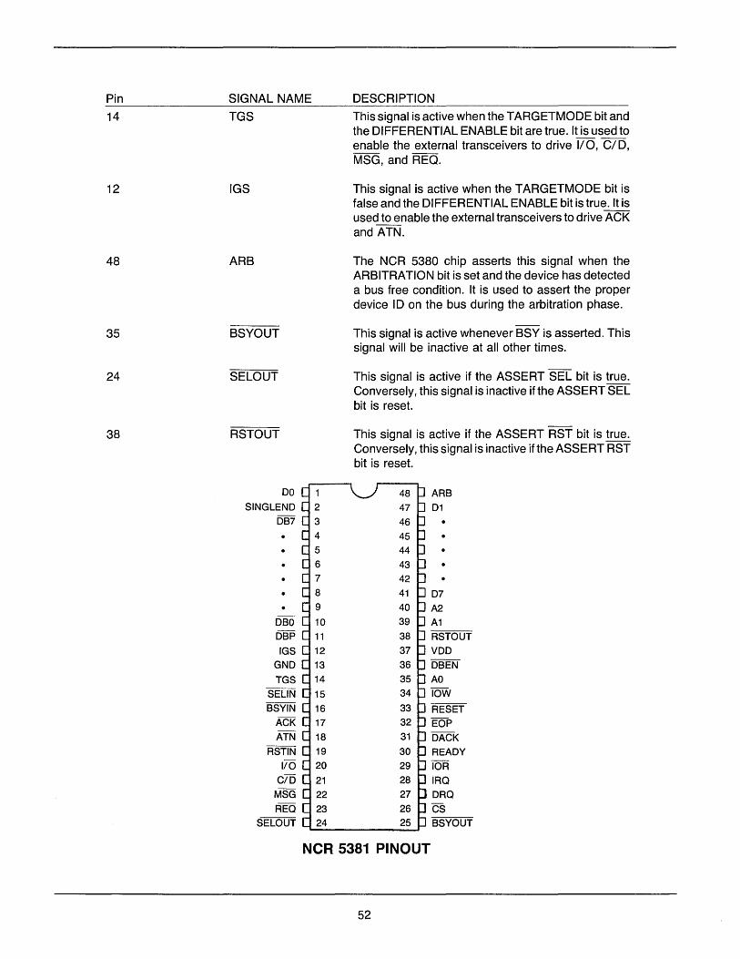
Pin
14
12
48
35
24
38
SIGNAL NAME
TGS
IGS
ARB
BSYOUT
SELOUT
RSTOUT
DO SINGLEND
DB7
DBO DBP IGS
GND TGS
SELIN BSYIN
ACK
C/D MSG REO
SELOUT
DESCRIPTION
This signal is active when the TARGETMODE bit and the DIFFERENTIAL ENABLE bit are true. It is used to enable the external transceivers to drive 1/0, CID, MSG, and REO.
This signal is active when the T ARGETMODE bit is false and the DIFFERENTIAL ENABLE bit is true. It is used to enable the external transceivers to drive ACK and ATN.
The NCR 5380 chip asserts this signal when the ARBITRATION bit is set and the device has detected a bus free condition. It is used to assert the proper device ID on the bus during the arbitration phase.
This signal is active whenever BSY is asserted. This signal will be inactive at all other times.
This signal is active if the ASSERT SEL bit is true. Conversely, this signal is inactive if the ASSERT SEL bit is reset.
This signal is active if the ASSERT RST bit is true. Conversely, this signal is inactive if the ASSERT RST bit is reset.
ARB D1
D7 A2
A1
RSTOUT VDD
DBEN AD lOW
RESET EOP DACK READY lOR
IRO
DRO
cs BSYOUT
NCR 5381 PINOUT
52
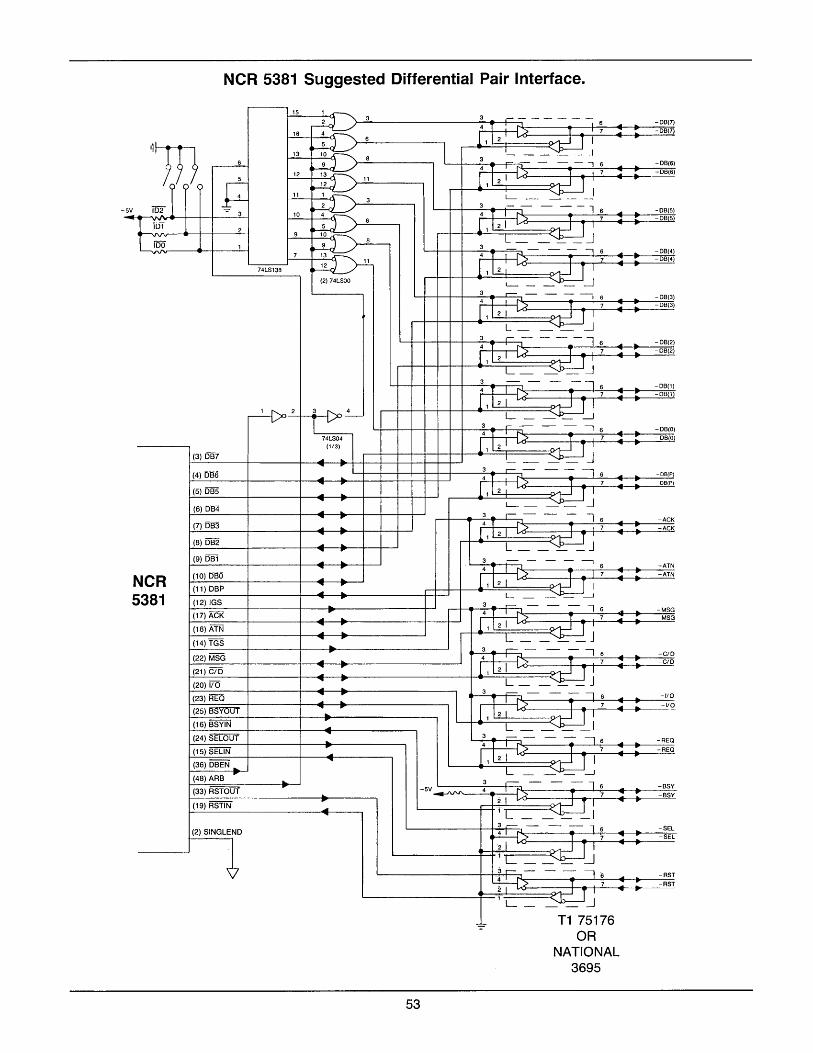
NCR 5381 Suggested Differential Pair Interface.
~lS~_~_~~~)-'::'3 _________ ~tb±!;;'3 _..-+-=--:;- - - - - -; 6 -OB(7)
16 I 4 '1:=.... 6 4::;. T 7 ~ -OB(7)
11m" 1-'1~3 --+-~";;"lso-ctK 8 lL--t--:3~1.,--2f I--~-::.-:::-=_~~-=-~I~-=-:::J~~~---j"~~~
----2.- 9 -, 6 ~ OB(6)
~5 j-.-:.:12'---1--~..;;13~~ 11 f--t..---rl'1 2; ::;. o-JI T I 7 ~ : -OB(6)
I j--!..:11--1-~:.....a2 F< 3 11 ~ _ ~_I sv TB2 1 -= 3 10 ~ ~1 211- -:- -~-I - 11 6 ~ -g:(~) I Tm-W
2 5 J} />-.::.6 __ --. L ~ .... ... '-1 """v"", vrv--__ -+---+------''-I 9 10;:=" J '---V"vl~V'0v--~--+-----l -l ~~: L)-L- ~! L - - - - I 6
NCR 5381
------
~ .. OB(4) r -OB(4) L __ j-7~T~1~24 11 ~ 7
74LS138 1 2: _ _vt-l_1 T : (2) 74LSOO ~ ~ ---l
(3) DB7
(4) 086
74LS04 (1/3)
~ .. ... ... ...
(5) DB5 ~ .. ....
(6) DB4 ... ~ "r'
(7) DB3 .. .... .. (8) 5B2 ... ..
... ..
~ -16 ~ .. OB(3)
~ .. ~ ..
~ ..
-OB(2) OB(2)
-OB(l) -OB 1)
tf2L-<':;>~ ___ t-.. --'-t-":"~_""~I-..... ____ ---=O:..:B=(O)
-.... -ACK
-ACK
(9) DBl ... .. 3 - - - - -, 6 _ -ATN
(10) DBO : .. ~j...<~0-____ Tf-'-.l.-..:.17_""''''I---I''~_-.::cA=TN ~(~11~)~D~B~P_-J~ ___ 1---<l=~~"~ _____ -+=±=T-t-~1~11~~2=~IL======~~~~~I ~
(12) IGS ..
(17) ACK
(18) ATN
(14) TGS
(22) MSG
(21) c/o
(20) I/O
(23) REO
(25) BSYOUT
(16) BSYIN
(24) SELOUT
(15) SELIN
(36) DBEN ...
(48) ARB ....
(33) RSTOUT
(19) RSTIN
(2) SINGLEND
t
... ...
.. ~ ..
~ .. .. .... ..
... .. ... .. ~ ~
... r'
... ... .. .. .... ... ... .. .. ..
..
53
3 r- ---'6 MSG -MSG
.. -c/o -c/o
I 110
-110
- - - - 1 6 - .. REO
-REO
-SV~~h~h==~;~=iI=s~ ___ ~_JLl~6_....r-._~B~S~Y -- :1 I V~o-"--~_-+T_~,--: 17_ .... ~ ___ -l .. ~_-"B""-'-SY
1L ____ I 3 1 6
~::?_ T '1
21 ~I 1L ___ ~ 3r----'s
... .. .... ..
T1 75176 OR
NATIONAL 3695
SEL -SEL
RST
-RST
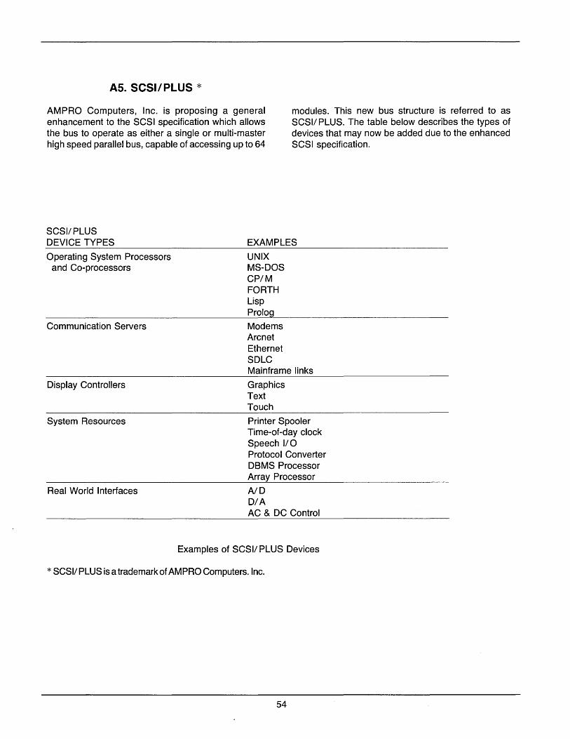
AS. SCSI/PLUS *
AMPRO Computers, Inc. is proposing a general enhancement to the SCSI specification which allows the bus to operate as either a single or multi-master high speed parallel bus, capable of accessing up to 64
modules. This new bus structure is referred to as SCSII PLUS. The table below describes the types of devices that may now be added due to the enhanced SCSI specification.
SCSI/PLUS DEVICE TYPES
Operating System Processors and Co-processors
Communication Servers
Display Controllers
System Resources
Real World Interfaces
EXAMPLES
UNIX MS-DOS CP/M FORTH Lisp Prolog
Modems Arcnet Ethernet SDLC Mainframe links
Graphics Text Touch
Printer Spooler Time-of-day clock Speech 1/0 Protocol Converter DBMS Processor Array Processor
AID D/A AC & DC Control
Examples of SCSII PLUS Devices
* SCSII PLUS is a trademark of AMPRO Computers. Inc.
54
SCSI! PLUS provides three functional additions to the SCSI specification which allow the bus to operate as either a loosely coupled distributed system bus or a low-cost single master I/O bus. As proposed, SCSI/ PLUS is a superset of the original specification, and its operation will not interfere with any existing SCSI im plementation.
To allow for more complex system configurations, SCSI/ PLUS provides Binary Arbitration and Binary Selection phases. The data bus represents a binary address and accommodates 64 physical bus devices, compared to eight in the current specification. In addition, four logical units may be associated with each bus device for a total of 256 logical bus devices. As in the SCSI specification, the arbitration phase is optional.
The addition of a master/ slave mode to the specification provides for a cost-effective single-master/ mUltislave configuration. This mode allows the design of SCSI/ PLUS Targets which have no on-board intelligence. An optional interrupt protocol allows these "dumb" targets to asynchronously notify the bus master that they desire service.
To encourage board-level interchangability, a recommended board size and interface connector is defined. The preferred board size is the single-wide Eurocard format with the double-wide card used as an option. The proposed interface connector is the DIN 41612-Type C connector. By using this form-factor and connector specification, bussed backplane or ribbon cable systems may be implemented.
The SCSI/ PLUS architectural concept has inherent advantages over traditional microprocessor backplane architectures. SCSI/ PLUS is CPU-independent, provides flexibility of form factor, operates across a ribbon cable bus, and allows both high-performance multi-master and low-cost single-master operation.
55
The NCR 5380 is an ideal part for designing an interface to connect to SCSI/ PLUS. Its simplicity provides the flexibility needed to support the defined protocol modifications, and its popularity with SCSI users guarantees plug compatibility with existing host adapters.
The NCR 5380 uses the Output Data Register to assert the proper device 10 onto the SCSI bus during the Arbitration and Selection phases. Since the user is not restricted by the number of bits he is allowed to assert on the SCSI data bus, the Binary Arbitration and Binary Selection phases can be easily supported. In a Target role the Select Enable Register may be used to generate an interrupt if any bit in this register matches the binary address on the SCSI bus. Here again the NCR 5380 does not restrict this implementation.
The ability to support the master/ slave operation requires independent control over the SCSI control signals by the bus slave devices and recognition by the bus master of the newly defined bus phase. The NCR 5380 provides independent signal control during Target operation and can be configured to generate an interrupt when a bus phase mismatch occurs if operating as an Initiator.
As in normal SCSI implementations, the use of on-chip bus transceivers significantly reduces parts count and provides for a highly reliable, cost effective SCSI/ PLUS design. An additional advantage of on-chip MOS transceivers is the low leakage current. The NCR 5380 maximum leakage current of 50 uA meets the SCSI/ PLUS bus load requirements. Up to 64 devices may occupy SCSI/ PLUS bus positions if low-leakage integrated circuits such as the NCR 5380 are used.
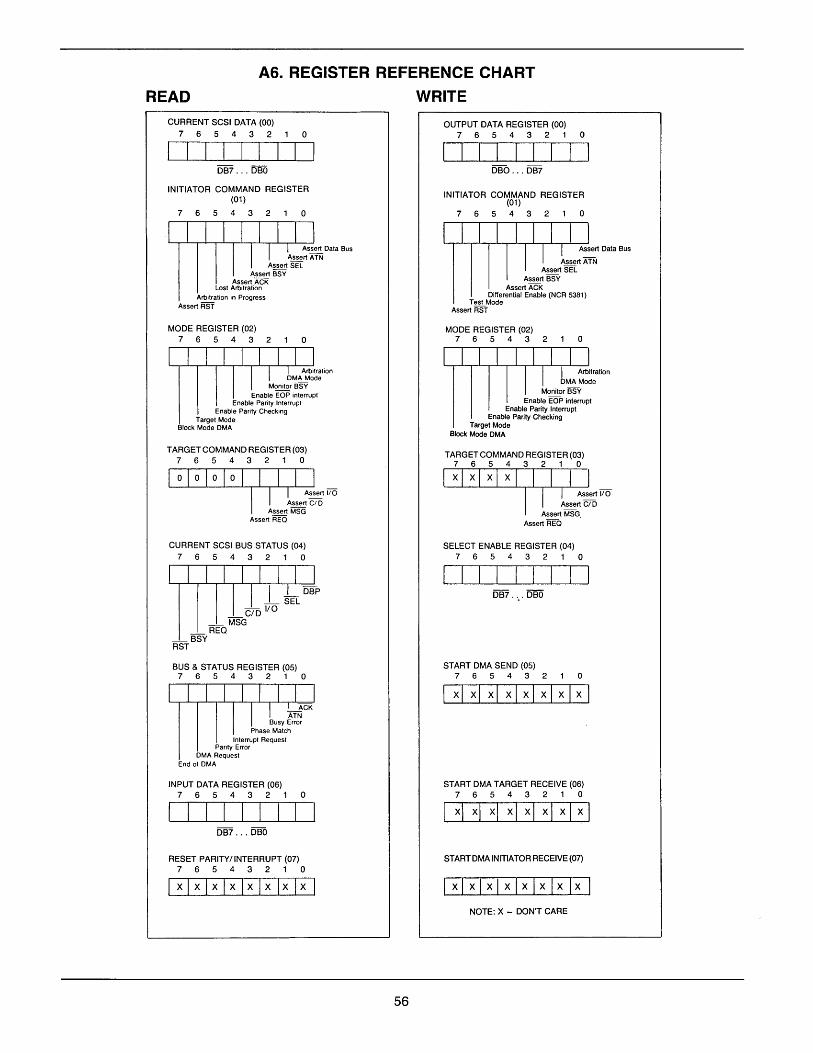
READ
A6. REGISTER REFERENCE CHART
WRITE
CURRENT SCSI DATA (00) 7 6 543 2 o
DB7 ... DBO
INITIATOR COMMAND REGISTER (01)
7 6 543 2 o
Assert Data Bus Assert ATN
Assert SEL Assert BSY
Assert ACK Lost Arbitration
Arbitration in Progress Assert RST
MODE REGISTER (02) 7 6 5 4 3 2 o
Enable EOP interrupt Enable Parity Interrupt
Enable Parity Checking Target Mode
Block Mode DMA
TARGET COMMAND REGISTER (03) 76543210
CURRENT SCSI BUS STATUS (04) 76543210
I _DBP _ SEL
C/D 110 _ MSG REQ
_BSY RST
BUS & STATUS REGISTER (05) 76543210
Interrupt Request Panty Error
DMA Request End of DMA
INPUT DATA REGISTER (06) 76543210
I I I I I I DB7 ... DBO
RESET PARITY/INTERRUPT (07) 76543210
IXIXIXIXIXIXIXIX I
56
OUTPUT DATA REGISTER (00) 76543210
DBO ... DB7
INITIATOR COMMAND REGISTER (01)
7 6 5 432 o
Assert ATN Assert SEL
Assert BSY Assert ACK
Differential Enable (NCR 5381) Test Mode
Assert RST
MODE REGISTER (02) 7 6 5 4 3 2 o
Enable EOP interrupt Enable Parity Interrupt
Enable Parity Checking Target Mode
Block Mode DMA
Assert REO
SELECT ENABLE REGISTER (04) 76543210
START DMA SEND (05) 7 6 543 2 o
I Xl Xl xl X I Xl X I X X
START DMA TARGET RECEIVE (06) 76543210
I xl xl xl X I X I X I X I X I
START DMA INITIATOR RECEIVE (07)
I xlXlxlXlxlxlx IX I NOTE: X = DON'T CARE

•
NCR Microelectronics Division 1635 Aeroplaza Drive Logic Products Marketing Colorado Springs, CO 80916 (303) 596·5612 or (800) 525·2252 TELEX 45·2457
..
Sp·1051 5/85


