1. A. Lewis, M. Isaacson, A. Harootunian, and A. Muray, “Development of a 500 Å spatial resolution light
microscope: I. light is efficiently transmitted through [lambda]/16 diameter apertures,” Ultramicroscopy 13(3), 227–231 (1984).
2. D. W. Pohl, W. Denk, and M. Lanz, “Optical stethoscopy: Image recording with resolution λ/20,” Appl. Phys.
Lett. 44(7), 651 (1984). 3. H. E. Jackson, S. M. Lindsay, C. D. Poweleit, D. H. Naghski, G. N. De Brabander, and J. T. Boyd, “Near field
measurements of optical channel waveguide structures,” Ultramicroscopy 61(1-4), 295–298 (1995).
4. S. Bourzeix, J. M. Moison, F. Mignard, F. Barthe, A. C. Boccara, C. Licoppe, B. Mersali, M. Allovon, and A. Bruno, “Near-field optical imaging of light propagation in semiconductor waveguide structures,” Appl. Phys.
Lett. 73(8), 1035–1037 (1998).
5. R. J. P. Engelen, T. J. Karle, H. Gersen, J. P. Korterik, T. F. Krauss, L. Kuipers, and N. F. van Hulst, “Local probing of Bloch mode dispersion in a photonic crystal waveguide,” Opt. Express 13(12), 4457–4464 (2005).
6. U. C. Fischer and D. W. Pohl, “Observation of single-particle plasmons by near-field optical microscopy,” Phys. Rev. Lett. 62(4), 458–461 (1989).
7. S. I. Bozhevolnyi, V. S. Volkov, E. Devaux, J.-Y. Laluet, and T. W. Ebbesen, “Channel plasmon subwavelength
waveguide components including interferometers and ring resonators,” Nature 440(7083), 508–511 (2006). 8. T. Zentgraf, J. Dorfmuller, C. Rockstuhl, C. Etrich, R. Vogelgesang, K. Kern, T. Pertsch, F. Lederer, and H.
Giessen, “Amplitude- and phase-resolved optical near fields of split-ring-resonator-based metamaterials,” Opt.
Lett. 33(8), 848–850 (2008). 9. M. L. Balistreri, J. P. Korterik, L. Kuipers, and N. van Hulst, “Local observations of phase singularities in
optical fields in waveguide structures,” Phys. Rev. Lett. 85(2), 294–297 (2000).
10. A. Nesci, R. Dändliker, and H. P. Herzig, “Quantitative amplitude and phase measurement by use of a heterodyne scanning near-field optical microscope,” Opt. Lett. 26(4), 208–210 (2001).
11. P. Tortora, M. Abashin, I. Märki, W. Nakagawa, L. Vaccaro, M. Salt, H. P. Herzig, U. Levy, and Y. Fainman,
“Observation of amplitude and phase in ridge and photonic crystal waveguides operating at 1.55 microm by use
of heterodyne scanning near-field optical microscopy,” Opt. Lett. 30(21), 2885–2887 (2005).
12. M. L. M. Balistreri, J. P. Korterik, L. Kuipers, and N. F. van Hulst, “Visualization of mode transformation in a
planar waveguide splitter by near-field optical phase imaging,” Appl. Phys. Lett. 79(7), 910 (2001). 13. E. Fluck, M. Hammer, A. M. Otter, J. P. Korterik, L. Kuipers, and N. F. van Hulst, “Amplitude and phase
evolution of optical fields inside periodic photonic structures,” J. Lightwave Technol. 21(5), 1384–1393 (2003).
14. J. Jose, F. B. Segerink, J. P. Korterik, J. L. Herek, and H. L. Offerhaus, “Imaging of surface plasmon polariton interference using phase-sensitive photon scanning tunneling microscope,” Appl. Phys. A (2011).
15. M. Spasenović, D. van Oosten, E. Verhagen, and L. Kuipers, “Measurements of modal symmetry in
subwavelength plasmonic slot waveguides,” Appl. Phys. Lett. 95(20), 203109 (2009).
#145587 - $15.00 USD Received 7 Apr 2011; revised 4 May 2011; accepted 26 May 2011; published 6 Jun 2011(C) 2011 OSA 20 June 2011 / Vol. 19, No. 13 / OPTICS EXPRESS 12014
16. U. Levy, M. Abashin, K. Ikeda, A. Krishnamoorthy, J. Cunningham, and Y. Fainman, “Inhomogenous dielectric
metamaterials with space-variant polarizability,” Phys. Rev. Lett. 98(24), 243901 (2007). 17. E. Schonbrun, Q. Wu, W. Park, T. Yamashita, C. J. Summers, M. Abashin, Y. Fainman, “Wave front evolution
of negatively refracted waves in a photonic crystal,” Appl. Phys. Lett. 90(4), 41113–3 (2007).
18. A. L. Campillo and J. W. P. Hsu, “Intensity and phase mapping of guided light in LiNbO3 waveguides with an interferometric near-field scanning optical microscope,” Appl. Opt. 42(36), 7149–7156 (2003).
19. H. W. Kihm, Q. H. Kihm, D. S. Kim, K. J. Ahn, and J. H. Kang, “Phase-sensitive imaging of diffracted light by
single nanoslits: measurements from near to far field,” Opt. Express 18(15), 15725–15731 (2010). 20. Y. Inouye and S. Kawata, “Near-field scanning optical microscope with a metallic probe tip,” Opt. Lett. 19(3),
159–161 (1994).
21. B. Knoll and F. Keilmann, “Enhanced dielectric contrast in scattering-type scanning near-field optical microscopy,” Opt. Commun. 182(4-6), 321–328 (2000).
22. R. Hillenbrand and F. Keilmann, “Complex optical constants on a subwavelength scale,” Phys. Rev. Lett.
85(14), 3029–3032 (2000). 23. I. Stefanon, S. Blaize, A. Bruyant, S. Aubert, G. Lerondel, R. Bachelot, and P. Royer, “Heterodyne detection of
guided waves using a scattering-type Scanning Near-Field Optical Microscope,” Opt. Express 13(14), 5553–
5564 (2005). 24. L. Gomez, R. Bachelot, A. Bouhelier, G. P. Wiederrecht, S.- Chang, S. K. Gray, F. Hua, S. Jeon, J. A. Rogers,
M. E. Castro, S. Blaize, I. Stefanon, G. Lerondel, and P. Royer, “Apertureless scanning near-field optical
microscopy: a comparison between homodyne and heterodyne approaches,” J. Opt. Soc. Am. B 23(5), 823–833 (2006).
25. B. Deutsch, R. Hillenbrand, and L. Novotny, “Near-field amplitude and phase recovery using phase-shifting
interferometry,” Opt. Express 16(2), 494–501 (2008). 26. B. Desiatov, I. Goykhman, and U. Levy, “Demonstration of submicron square-like silicon waveguide using
The ability to measure light in the near field by a Near Field Scanning Optical Microscope
(NSOM) plays an important role in high resolution imaging [1,2]. Nowadays, NSOM is
widely used for the characterization of nano photonic structures, e.g. nano waveguides [3,4],
photonic crystals [5], plasmonic structures [6,7] and metamaterials [8].
Typically an NSOM measures the intensity of the light and does not reveal the complex
nature of the measured electromagnetic field. In order to measure both the phase and the
amplitude of the field, various systems have been proposed and demonstrated both in aperture
and in apertureless configurations. For example, in an Aperture Heterodyne NSOM the light
is collected by the probe and combined with a reference arm to allow simultaneous
measurement of the amplitude and the phase of the light [9–11]. This technique uses Acousto
Optic Modulators (AOMs) in order to shift the frequency of the reference arm with respect to
the collecting arm and was used for the characterization of large variety of nano-photonic
devices [12–17]. These AOMs are integrated into an interferometer that consists of an
existing NSOM apparatus. In other works [18,19], the phase and amplitude measurement has
been obtained by introducing an additional phase modulator into one of the arms of the
interferometer, a modulation that introduces several spectral components in the reference arm
which in turn interfere with the probe arm.
In order to maintain constant distance from the device under test (DUT) and to improve
the signal whilst measuring fragile samples having abrupt topographical variations one can
use the NSOM scanning in tapping mode, in which the NSOM probe is oscillating with
respect to the sample. This mode of operation is often exploited in Apertureless NSOMs [20]
(ANSOM), where the light scattered from a metallic tip is collected in the far field and is
demodulated at one of the harmonies of the tip’s oscillating frequency in order to eliminate
background scattering [21]. Such ANSOMs have been combined with heterodyne systems
where, various combinations of the probes frequency and AOM frequency have been used in
order to extract both the phase and the amplitude of the signal [22–25].
In this paper, we exploit the intrinsic modulation of the NSOM tip operating in tapping
mode to measure the phase of the signal in the near field using an aperture NSOM. The
#145587 - $15.00 USD Received 7 Apr 2011; revised 4 May 2011; accepted 26 May 2011; published 6 Jun 2011(C) 2011 OSA 20 June 2011 / Vol. 19, No. 13 / OPTICS EXPRESS 12015
system is based on an all-fiber interferometer. We show this intrinsic modulation introduces
several spectral components that interfere with the reference arm and introduce a signal that
contains information representing the phase and the amplitude of the signal. The method is
compact, cost effective, align-free, shot-noise limited and does not require external
modulators. The system can be integrated to an existing NSOM setup in relative ease and has
high potential as a characterization tool of various nanophotonic structures. The benefits of
the system are demonstrated through the near field characterization of several silicon
nanophotonic devices, including straight and serpentine like ridge waveguides as well as the
recently demonstrated local oxidation of silicon (LOCOS) waveguides [26]. To the best of
our knowledge, near field phase measurements of LOCOS waveguides are demonstrated here
for the first time.
The paper is structured as follows: Section 2 outlines the concept of operation and
describes the experimental setup. In section 3 we demonstrate the experimental results
obtained with the system. Section 4 concludes the paper.
2. Concept of operation and experimental arrangement
The experimental setup is illustrated schematically in Fig. (1). A 1550 nm wavelength TE (in
plane) polarized light emitted from a diode laser is split by a 90/10 polarization maintaining
(PM) fiber beam splitter (BS) where the majority of light is sent via a PM lensed fiber into a
silicon waveguides (WG) serving as the DUT. Metal coated NSOM probes (With an apex
varying between 250 and 300 nm. This aperture size determines roughly the resolution of our
system) are brought into proximity with the DUT and kept in contact with its surface using
the tapping feedback mechanism in a commercial NSOM system (Nanonics MultiView
4000). The light is collected by the NSOM tip, combined with the reference arm using a
50/50 PM BS and detected by an InGaAs Photo Detector (PD, Thorlabs DET01CFC). The
NSOM probe is modulated at a frequency fprobe around 40 KHz, which is the characteristic
eiqen-frequency of the tuning fork of the tip. Such a relatively low frequency component can
be detected and demodulated with relative ease with a standard detector and Lock In
Amplifier (LIA, SR-830) either in quadrature (Y) or in phase (X) modes.
Fig. 1. Experimental arrangement of the NSOM probe modulated interferometer. (BS – Beam Splitter, DUT – Device Under Test, PD – Photo Detector, LIA – Lock In Amplifier)
As in any interferometer, special attention is needed in order to avoid phase drifts due to
temperature, and/or mechanical instabilities. This is achieved by: 1- setting the optical paths
of the interferometer arms to equal lengths in order to be immune to thermo-mechanical and
frequency drifts, and 2- by thermal and mechanical insulation of the system using a “Minus-
K” bench top vibration isolation platform and a “home made” acoustic hood. The former has
the additional benefit of protecting the probe from getting damaged.
In order to evaluate the signal derived from the LIA at the tip's frequency, we assume that
the mechanical modulation of the probe is converted to an amplitude modulation of the
probed light while interacting with the evanescent field propagating along the WG. A
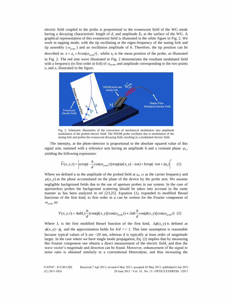
schematic graphic representation of the process is illustrated in Fig. 2, where the tuning fork
attached to the NSOM probe is illustrated in contact with the WG. We assume that the
#145587 - $15.00 USD Received 7 Apr 2011; revised 4 May 2011; accepted 26 May 2011; published 6 Jun 2011(C) 2011 OSA 20 June 2011 / Vol. 19, No. 13 / OPTICS EXPRESS 12016
electric field coupled to the probe is proportional to the evanescent field of the WG mode
having a decaying characteristic length of d, and amplitude E0 at the surface of the WG. A
graphical representation of this evanescent field is illustrated in the white figure in Fig. 2. We
work in tapping mode, with the tip oscillating at the eigen-frequency of the tuning fork and
tip assembly ( probe ) and an oscillation amplitude of h. Therefore, the tip position can be
described as 0 cos( )probez z h t , whilst z0 is the mean position of the probe, as illustrated
in Fig. 2. The red sine wave illustrated in Fig. 2 demonstrates the resultant modulated field
with a frequency (to first order in h/d) of ωprobe and amplitude corresponding to the two points
z1 and z2 illustrated in the figure.
Fig. 2. Schematic illustration of the conversion of mechanical modulation into amplitude
modulation of the probed electric field: The NSOM probe oscillates due to modulation of the tuning fork and probes the evanescent decaying field, resulting in a modulated electric field.
The intensity, at the photo-detector is proportional to the absolute squared value of this
signal arm, summed with a reference arm having an amplitude b and a constant phase 0 ,
yielding the following expression:
2
0( , , ) exp( cos( ))exp( ( , ) ) exp( )probe
hV x y t a t i x y i t b i t i
d (1)
Where we defined a as the amplitude of the probed field at z0, ω as the carrier frequency and
( , )x y as the phase accumulated on the plane of the device by the probe arm. We assume
negligible background fields due to the use of aperture probes in our system. In the case of
apertureless probes the background scattering should be taken into account in the same
manner as has been analyzed in ref [23,25]. Equation (1), expanded to modified Bessel
functions of the first kind, to first order in a can be written for the Fourier component of
Where I1 is the first modified Bessel function of the first kind, ( , )x y is defined as
0( , )x y and the approximation holds for h/d << 1. This later assumption is reasonable
because typical values of h are ~20 nm, whereas d is typically at least order of magnitude
larger. In the case where we have single mode propagation, Eq. (2) implies that by measuring
this Fourier component one obtains a direct measurement of the electric field, and thus the
wave vector’s magnitude and direction can be found. Moreover, enhancement of the signal to
noise ratio is obtained similarly to a conventional Heterodyne, and thus increasing the
#145587 - $15.00 USD Received 7 Apr 2011; revised 4 May 2011; accepted 26 May 2011; published 6 Jun 2011(C) 2011 OSA 20 June 2011 / Vol. 19, No. 13 / OPTICS EXPRESS 12017
intensity in the reference arm can lead to a shot noise limited detection system, as reported in
ref [10]. We shall refer to this demodulated signal as the Phase NSOM (PNSOM) signal. In
the case where the probed electric field consists of several k-vectors (multi mode
propagation), the Fourier component will be a superposition of terms such as in Eq. (2) in the
following manner:
( , ) 2 cos( )cos( )n n probe
n n
hV r t b a t
d (3)
As before, the effective indices of refraction can be derived by Fourier analysis of the
signal. However, in this case, caution should be taken in the interpretation of the amplitudes
of the different propagation modes, due to the possible differences between the evanescent
lengths dn. These differences can be compensated in the Fourier analysis if we assume all the
interactions to be pure evanescent, and use the conservation of momentum: 2 2 2 2
0 0 effk k n d .
In addition, due to the signal being inverse proportional to the decaying length d, delocalized
modes that have decaying lengths much larger than the oscillation amplitude h might suffer a
degradation in signal to noise ratio due to the small value of the modulation depth h/d.
However, this may be compensated by the amplification of the heterodyne approach.
3. Experimental results
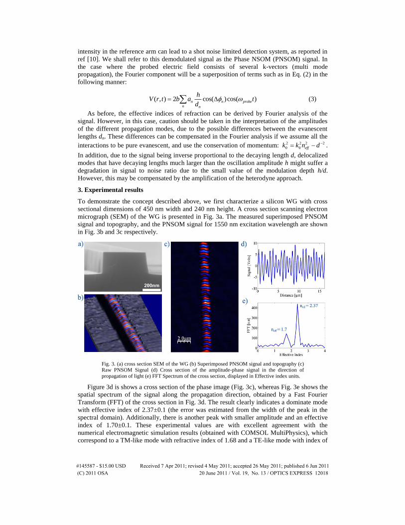
To demonstrate the concept described above, we first characterize a silicon WG with cross
sectional dimensions of 450 nm width and 240 nm height. A cross section scanning electron
micrograph (SEM) of the WG is presented in Fig. 3a. The measured superimposed PNSOM
signal and topography, and the PNSOM signal for 1550 nm excitation wavelength are shown
in Fig. 3b and 3c respectively.
Fig. 3. (a) cross section SEM of the WG (b) Superimposed PNSOM signal and topography (c) Raw PNSOM Signal (d) Cross section of the amplitude-phase signal in the direction of
propagation of light (e) FFT Spectrum of the cross section, displayed in Effective index units.
Figure 3d is shows a cross section of the phase image (Fig. 3c), whereas Fig. 3e shows the
spatial spectrum of the signal along the propagation direction, obtained by a Fast Fourier
Transform (FFT) of the cross section in Fig. 3d. The result clearly indicates a dominate mode
with effective index of 2.37±0.1 (the error was estimated from the width of the peak in the
spectral domain). Additionally, there is another peak with smaller amplitude and an effective
index of 1.70±0.1. These experimental values are with excellent agreement with the
numerical electromagnetic simulation results (obtained with COMSOL MultiPhysics), which
correspond to a TM-like mode with refractive index of 1.68 and a TE-like mode with index of
#145587 - $15.00 USD Received 7 Apr 2011; revised 4 May 2011; accepted 26 May 2011; published 6 Jun 2011(C) 2011 OSA 20 June 2011 / Vol. 19, No. 13 / OPTICS EXPRESS 12018
refraction of 2.33. The existence of the TM mode in our WG can be explained by the TE/TM
conversion in the waveguide as a result of fabrication imperfections and a bent section in the
WG. This bend is needed for PNSOM measurements as it allows spatial separation between
the guided modes and the radiation modes emanating from the coupling region between the
lensed fiber and the WG. We note that concluding the actual amplitude ratio between these
two modes of the amplitude from the FFT figure might be misleading. These measured
amplitudes can differ from the real amplitudes due to two reasons. The first, mentioned before
and illustrated by Eq. (3), is the fact that our PNSOM signal is linear with the inverse of the
evanescent length, and thus each mode has a different evanescent length yielding different
amplitudes in the FFT. The second is due to the vectorial transfer function of the NSOM tip,
which is anticipated to be stronger for the TE-like mode [27].
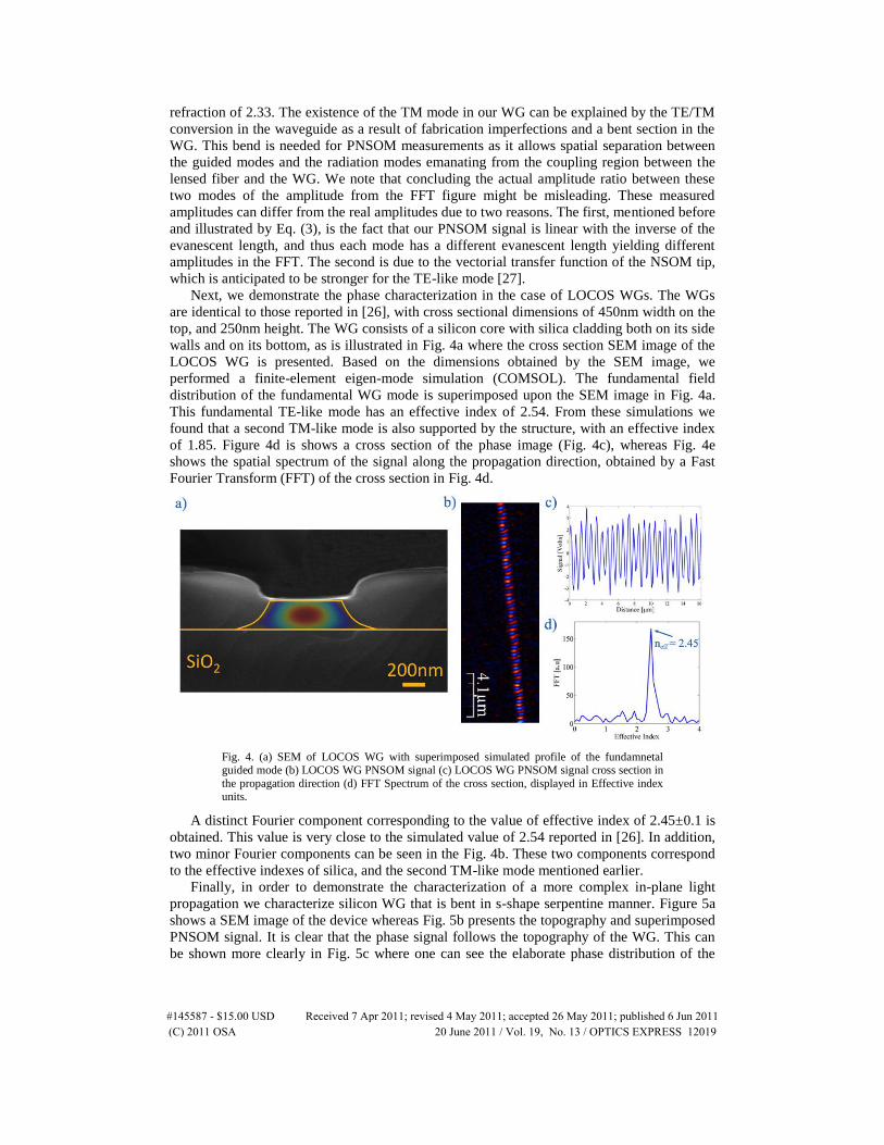
Next, we demonstrate the phase characterization in the case of LOCOS WGs. The WGs
are identical to those reported in [26], with cross sectional dimensions of 450nm width on the
top, and 250nm height. The WG consists of a silicon core with silica cladding both on its side
walls and on its bottom, as is illustrated in Fig. 4a where the cross section SEM image of the
LOCOS WG is presented. Based on the dimensions obtained by the SEM image, we
performed a finite-element eigen-mode simulation (COMSOL). The fundamental field
distribution of the fundamental WG mode is superimposed upon the SEM image in Fig. 4a.
This fundamental TE-like mode has an effective index of 2.54. From these simulations we
found that a second TM-like mode is also supported by the structure, with an effective index
of 1.85. Figure 4d is shows a cross section of the phase image (Fig. 4c), whereas Fig. 4e
shows the spatial spectrum of the signal along the propagation direction, obtained by a Fast
Fourier Transform (FFT) of the cross section in Fig. 4d.
Fig. 4. (a) SEM of LOCOS WG with superimposed simulated profile of the fundamnetal guided mode (b) LOCOS WG PNSOM signal (c) LOCOS WG PNSOM signal cross section in
the propagation direction (d) FFT Spectrum of the cross section, displayed in Effective index units.
A distinct Fourier component corresponding to the value of effective index of 2.45±0.1 is
obtained. This value is very close to the simulated value of 2.54 reported in [26]. In addition,
two minor Fourier components can be seen in the Fig. 4b. These two components correspond
to the effective indexes of silica, and the second TM-like mode mentioned earlier.
Finally, in order to demonstrate the characterization of a more complex in-plane light
propagation we characterize silicon WG that is bent in s-shape serpentine manner. Figure 5a
shows a SEM image of the device whereas Fig. 5b presents the topography and superimposed
PNSOM signal. It is clear that the phase signal follows the topography of the WG. This can
be shown more clearly in Fig. 5c where one can see the elaborate phase distribution of the
#145587 - $15.00 USD Received 7 Apr 2011; revised 4 May 2011; accepted 26 May 2011; published 6 Jun 2011(C) 2011 OSA 20 June 2011 / Vol. 19, No. 13 / OPTICS EXPRESS 12019
light propagating through the device. Clear slanted phase fronts that follow the topography of
the WG are shown. In addition, one can identify phase fronts with a longer wave-length that
do not follow that WG. These phase fronts are most likely radiation and scattering modes that
originate from sidewall roughness and from the bending of the WG. In Fig. 5d the electric
field obtained via a finite difference time domain (FDTD) simulation of this s-shaped WG are
presented. The simulation results contain the same features that were observed in the
measurements, including both the guided and the radiation modes (the radiation modes part in
the image has been amplified in order to improve their visibility).
Fig. 5. (a) SEM image of Si serpentine WG (b) Superimposed PNSOM signal on AFM
topography (c) PNSOM raw signal (d) FDTD simulation of the s-shaped WG field distribution, in order to improve the visibility the background of the image is amplified.
4. Summary
An innovative method which exploits the intrinsic amplitude modulation of an aperature
NSOM probe in tapping mode is experimentally demonstrated and used for the
characterization of several sub-micron silicon light guiding devices. We measured the phase
profile in these different WGs and used these measurements to perform a modal analysis that
was found to be in good agreement with computer simulations. The demonstrated method is
compact, cost effective, align-free, and shot-noise limited. Such a system can be integrated to
an existing NSOM setup, in relative ease and is thus a potential candidate for the
characterization tool of various nanophotonic structures.
Acknowledgments
The authors thank L. (Kobus) Kuipers, Nissim Ben Yosef and Dan Marom for fruitful
discussions. L. Stern gratefully acknowledges the support of the Peter Brojde Center for
Innovative Engineering and Computer Science. I. Goykhman acknowledges the Eshkol
fellowship from the ministry science and technology. The waveguides were fabricated at the
Center for Nanoscience and Nanotechnology, The Hebrew University of Jerusalem.
#145587 - $15.00 USD Received 7 Apr 2011; revised 4 May 2011; accepted 26 May 2011; published 6 Jun 2011(C) 2011 OSA 20 June 2011 / Vol. 19, No. 13 / OPTICS EXPRESS 12020