71
N'ECm Inc. FLOPPY DISK CONTROLLER USERS' MANUAL Five Militia Drive/Lexington, Massachusetts 02173 Telephone (617) 862-6410 Rev/2 J.LPD372 Telex 92-3434

N'ECm Inc.
FLOPPY DISK CONTROLLER USERS' MANUAL
Five Militia Drive/Lexington, Massachusetts 02173 Telephone (617) 862-6410
Rev/2
J.LPD372
Telex 92-3434

NEC MICROCOMPUTERS, INC.
uPD372D
LSI FLOPPY DISK CONTROLLER CHIP
USERS' MANUAL
March 11, 1977
The NEC uPD372D is a high performance N-channel LSI floppy disk controller designed to- interface between most minicomputers or microprocessors and most floppy disk drives.
The uPD372D is the most versatile floppy disk controller chip available.
FEATURES - Compatible with IBM3740 format
- Compatible with Shugart Minifloppy format
- Compatible with many other formats
- Generates and checks Cyclic Redundancy Characters
- Initiates operations at address marks or physical index
- Formats clear disks
- Handles up to four floppy disk drives
- Can read or write on one drive while simultaneously track seeking on another
- Track stepping rate and step pulse width are programmable
- Sector size programmable from one byte to one sector per track
- Data transfer rate easily changed
- Standard power supply voltages +12V, +5V, -5V
The uPD372D is compatible with most floppy disk drives including:
Calcomp 140 Pertec FD400
CDC BR803 Potter DD4740
GSI 050 Remex RFS7400
GSI 110 Shugart SA400
Innovex 210 Shugart SA900
Orbis 74 Sycor 145
Persci 75
2
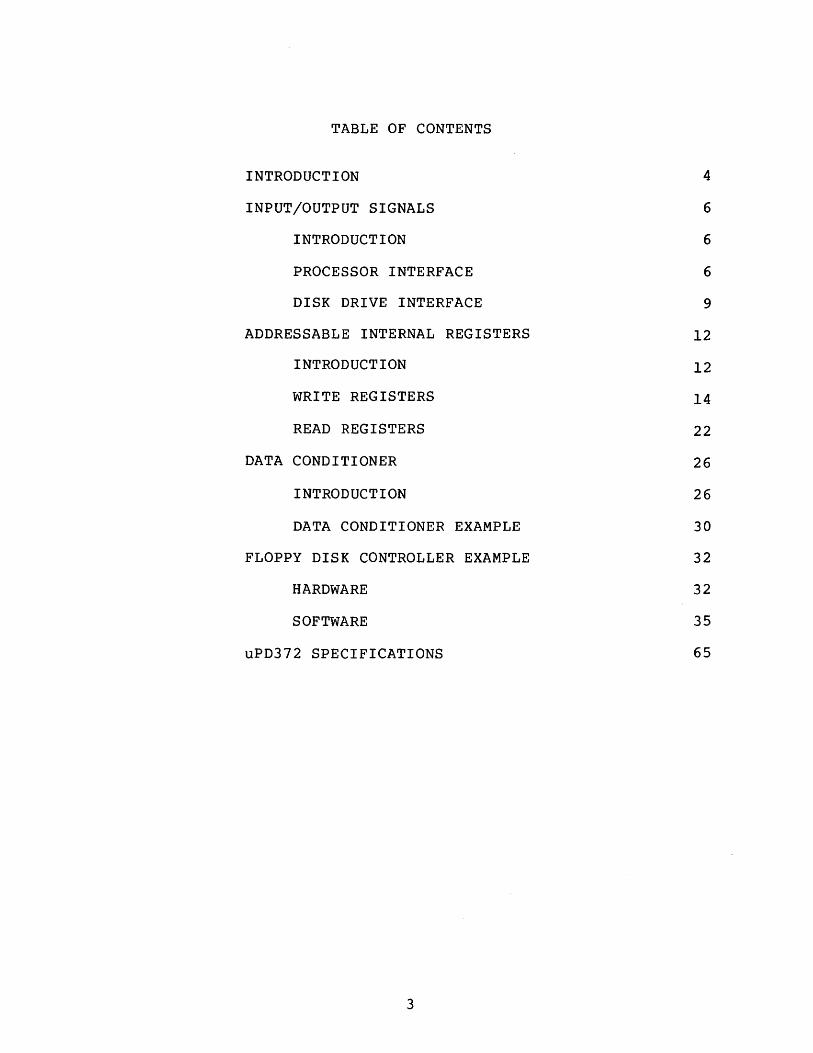
TABLE OF CONTENTS
INTRODUCTION
INPUT/OUTPUT SIGNALS
INTRODUCTION
PROCESSOR INTERFACE
DISK DRIVE INTERFACE
ADDRESSABLE INTERNAL REGISTERS
INTRODUCTION
WRITE REGISTERS
READ REGISTERS
DATA CONDITIONER
INTRODUCTION
DATA CONDITIONER EXAMPLE
FLOPPY DISK CONTROLLER EXAMPLE
HARDWARE
SOFTWARE
uPD372 SPECIFICATIONS
3
4
6
6
6
9
12
12
14
22
26
26
30
32
32
35
65

INTRODUCTION
The uPD372 may be interfaced directly to a host processor as shown in Figure 1 or it may be interfaced to a controller processor which in turn is interfaced to the host processor as shown in Figure 2. Most processors interfaced to the uPD372 must, when reading from or writing a record on the disk, be completely dedicated to the task of controlling the disk drive(s). These periods may last several milliseconds. If the nature of the other tasks performed by the host processor allows them to be neglected for this length of time, then the uPD372 may be interfaced directly to the host processor. Otherwise, a controller processor is required.
Whichever approach is chosen, the floppy disk drive control workload is shared between the uPD372 hardware and the processor(s) software.
The uPD372 converts information, which the software transmits to uPD372 internal registers, into commands and serial data which are transmitted to the disk drive(s). The uPD372 converts status signals and serial data from the drives into register information which is read by the software. The uPD372 also controls the timing of most disk operations and performs many other tasks such as Cyclic Redundancy Character generation and checking.
The software tasks are usually divided into two groups as shown in Figures 1 and 2. The Drive Handling Routines control sector reading and writing and track seeking. The Floppy Disk Operating System contains the executive programs which instruct the Drive Handling Routines to read or write a particular sector on a particular track. The Floppy Disk Operating System programs also decide from what area of memory write data should be taken and into what area of memory read data should be stored.
A uPD372 interface between a uPD8080A microprocessor and an IBM3740 compatible drive is shown in the right hand side of Figure 10 in the FLOPPY DISK CONTROLLER EXAMPLE section. This circuit may be interfaced directly to a uPD8080A host processor or to a uPD8080A controller processor similar to the example shown in the left hand side of Figure 10.
Since the disk drive(s) operate under program control, complete uPD8080A assembly listings of the Drive Handling Routines with extensive comments are included in the FLOPPY DISK CONTROLLER EXAMPLE section. The listings describe the sequence of events of each disk operation. Although the sequences are specific to IBM3740 format and to a uPD8080A microprocessor, sequences for other formats are very similar in most respects and the uPD8080A instructions used are largely limited to simple INPUTS, OUTPUTS, CONDITIONAL JUMPS, etc., which are similar to those of other processors.
4

I uPD372 I I r--- DRIVERS · I I I I I
HOST PROCESSOR I I
FLOPPY CISK OPERATING
SYSTEM
HOST PROCESSOR
FLOPPY DISK OPERATING
SYSTEM
I I PROCESSOR I---
I • INTERFACE ~ RECEIVERS
I DRIVE I I HANDLING I ROUTINES I I
I I I
I---- DATA I I CONDITIONER
I I I I I L _______________ ...J
FIGURE 1 uPD372 INTERFACED DIRECTLY TO HOST PROCESSOR (15-20 CHIPS)
r -------Fu,m 0 15K -cON-fficiLER- - - - - - - i I I
I I I I I I CONTROLLER
PROCESSOR
I I I--- PROCESSOR I---• INTERFACE
I DRIVE
I HANDLING ROUTINES
I I I
L __ _
FIGURE 2
uPD372 -
-
-
DRIVERS
RECEIVERS
DATA CONDITIONER
I I I I I I I · I I I I I · I I I
__..J
FLOPPY DISK DRIVE(S)
COMMANDS AND WRITE DATA
STATUS
READ DATA
FLOPPY DISK DRIVE(S)
COMMANDS AND WRITE DATA
STATUS
READ DATA
uPD372 I NTERFACED TO HOST PROCESSOR THROUGH CONTROLLER PROCESSOR (34-40 CH IPS)
5

INPUT/OUTPUT SIGNALS
INTRODUCTION
Figure 3 shows the input/output signals of the uPD372 grouped into 10 categories.
RESET REGISTER SELECT COMMANDS INTERRUPT REQUEST DATA BUS TIMING WRITE DATA DISK DRIVE COMMANDS READ DATA DISK DRIVE STATUS MISCELLANEOUS
The REGISTER SELECT COMMANDS control Data Transfers from the DATA BUS to the 6 uPD372 write registers. The contents of the write registers are translated by the uPD372 into WRITE DATA and DISK DRIVE COMMANDS. The REGISTER SELECT COMMANDS also control Data Transfers from the 3 uPD372 read registers to the data bus. The processor may then read the DISK DRIVE STATUS and READ DATA from the data bus.
The processor generates DISK DRIVE COMMANDS by manipulating bits in the uPD372 write registers and the DISK DRIVE STATUS signals control the state of bits in the read registers. To avoid repetition the signals in these two categories are described in the ADDRESSABLE INTERNAL REGISTERS section only. All other input/output signals are described below.
Processor Interface
Reset
Pin 1 RST (Reset)
A logic one at pin 1 causes a general reset of the uPD372. For a list of signals and registers affected, see RST-bit 7 of Write Register 0 (WR0) in the ADDRESSABLE INTERNAL REGISTERS section.
6

PROCESSOR INTERFACE
RESET
2 REGISTER WRITE/READ SELECT
REGISTER DATA STROBE REGISTER SELECT REGISTER SELECT 2 COMMANDS
REGISTER SELECT 1
REG ISTER SELECT 0
INTERRUPT REQUEST 17
DATA BUS 0 31
DATA BUS 1
DATA BUS 2
DATA BUS 3 DATA BUS
DATA BUS
DATA BUS 5
DATA BUS 6~
DATA BUS 7~
TlMING{
13 WRITE CLOCK
01
02
uPD372
RST WD
HLD
W/R LCT
OS WFR
RS2 WE
RSl SID
RS0 SOS
UBI
UB0
REQ UAl
UA0
RD
DB6 WFT
DB? T00
CKS
AWL
VSS vec VDD
40
GND -5V +5V +12V
FIGURE 3 INPUT/OUTPUT SIGNALS
7
DISK DRIVE INTERFACE
18 WRITE DATA ) TO
DISK DRIVE
19 HEAD LOAD
22 LOW CURRENT
23 WRITE FAULT RESET
24 WR I TE CURRENT ENABLE
25 STEP IN OR DIRECTION DISK DRIVE
26 STEP OUT OR STEP
COMMANDS
27 DISK DRIVE B1 SELECT
28 DISK DRIVE B0 SELECT
29 DISK DRIVE Al SELECT
30 DISK DRIVE A0 SELECT
10 READ CLOCK } FROM READ DATA DISK DRIVE
INDEX
WRITE FAULT
TRACK ZERO DISK DRIVE
STATUS
DISK DRIVE A READY
DISK CRIVE BREADY
15 CLOCK STATUS }MISC. 16 ALWAYS LOW

Register Select Commands and Data Bus
Pin 2 W/R (Register Write/Read Select)
Pin 3 DS (Register Data Strobe)
Pins 4-6 RS0-RS2 (Register Address)
Pins 31-38 DB0-DB7 (Data Bus)
W/R, DS and RS0-RS2 control Data Bus transfers between the uPD372 and the processor as follows:
Writing into a uPD372 register
When W/R isa logic one, information the processor places on DB0-DB7 is written into the uPD372 Write Register selected by RS0-RS2. The information is written at the time of the trailing edge of each 02 which occurs while DS is a logic one.
Reading from a uPD372 register
When W/R is a logic zero, information from the uPD372 Read Register selected by RS0-RS2 is placed on DB0-DB7 to be read by the processor. The information remains on DB0-DB7 as long as DS is a logic one. See uPD372 SIGNAL TIMING DIAGRAM, Figure 12 for exact timing.
NOTE: The logic condition which places uPD372 READ Register information on the Data Bus is DS.W!R·RS2. If these three signals are allowed to change asynchronously with respect to each other, care must be taken to insure that this condition does not become true inadvertantly. The simplest method is to require that W/R and RS2 must not change state while DS is a logic one.
NOTE: RS0 and RSI must not change state during the period from l50ns before until l0ns after the trailing edge of 01 or else register contents and DISK DRIVE COMMANDS may be modified. A simple method to accomplish this is to use a dual flip-flop to synchronize changes in RS0 and RSI with the leading edge of 02(TTL) as shown in Figure 10.
8

Interrupt Request
Pin 17 REQ (Interrupt Request)
Interrupt requests are generated by the uPD372 only while STT (Start-bit 5 of WR3) is true. Two types of interrupt requests occur -- Index Requests and Data Requests.
Index Requests occur once per disk revolution when the physical index hole passes a photodetector. See IRQ-bit 1 of Read Register 0 (RR0) in the ADDRESSABLE INTERNAL REGISTERS section.
Data Requests begin during disk reading after an address mark is read and then occur each time an eight-bit byte, assembled from disk serial data, is available to be read by the processor program. Data requests occur during disk writing or formatting each time an eight-bit byte is required from the processor program. See DRQ-bit 0 of Read Register 0 (RR0) in the ADDRESSABLE INTERNAL REGISTERS section.
Timing Signals
Pin 41 01
Pin 42 02
The uPD372 requires two MOS level clock signals, 01 and 02. A uPD8224 generates both 01 and 02 as well as a TTL level 02. If the uPD372 is interfaced to a uPD8080A microprocessor and if both devices are in the same proximity, they may share a uPD8224 as shown in Figure 10.
Pin 13 WCK (Write Clock)
WCK determines the bit transfer rate to the selected disk drive while writing. IBM standard drives require a 500KHz WCK. The Shugart Minifloppy requires a 250KHz WCK. Other standards may require different WCK frequencies. In each case the WCK frequency should be twice the bit transfer rate.
DISK DRIVE INTERFACE
write Data
Pin 18 WD (Write Data)
Serial Frequency Modulated (FM) code to be written on a floppy disk leaves the uPD372 at pin 18. Pin 18 should be connected to the WRITE DATA input of the selected disk drive.
9

Disk Drive Commands
The following commands to the disk drive(s) are generated under program control by modifying the contents of uPD372 write Registers. The description of each command may be found in the ADDRESSABLE INTERNAL REGISTERS section under the appropriate write register and register bit.
Pin 19
Pin 22
Pin 23
Pin 24
Pin 25
Pin 26
Pin 27
Pin 28
Pin 29
Pin 30
Read Data
HLD (Head Load)
LCT (Low Current)
WFR (Write Fault Reset)
WE (Write Current Enable)
SOS (Step Out or Step)
SID (Step In or Direction)
UBI (Disk Drive Bl Select)
UB0 (Disk Drive B0 Select)
UAI (Disk Drive Al Select)
UA0 (Disk Drive A0 Select)
Pin 10 RCK (Read Clock)
Pin 11 RD (Read Data)
See Write Register 0 (WR0) bit 3
See WR0 bit 2
See WR0 bit 1
See WR3 bits 2 and 4
See WR4 bit 5
See WR4 bit 6
See WR4 bit 1
See WR4 bit 0
See WRI bit 1
See WRI bit 0
RD is a changing logic level updated by each data and clock pulse in the raw data read from the selected disk drive. RCK is a clock the positive transition of which strobes RD into the uPD372. Both signals are derived from the raw data by the DATA CONDITIONER circuit. See the DATA CONDITIONER section for a complete description of RCK and RD.
10

Disk Drive Status Signals
The following status signals from the disk drive(s) each control the logic level of a bit in uPD372 Read Registers 0 and 1 (RR0 and RRl). By reading the contents of these registers the processor program senses the disk drive status signals. A description of each status signal may be found in the ADDRESSABLE INTERNAL REGISTERS section under the appropriate read register and bi t.
Pin 7 IDX (Index) See Read Register 0 (RR0) bit 1
Pin 8 WFT (Write Fault) See RRI bit 2
Pin 9 T00 (Track Zero) See RRI bit 6
Pin 12 RYA (Disk Drive A Ready) See RRI bit 3
Pin 14 RYB (Disk Drive B Ready) See RR0 bit 6
Miscellaneous
Pin 15 CKS (Clock Status)
A logic one at CKS indicates that the uPD372 has been commanded (by WCS, bit 6-WR3) to operate with timing signals from the Write Clock (WCK, pin 13). A logic zero at CKS indicates that the uPD372 has been commanded (by RCS, bit 7-WR3) to operate with timing signals from the Read Clock (RCK, pin 10).
Pin 16 AWL (Always Low)
AWL is a logic zero output under all normal operating conditions.
11
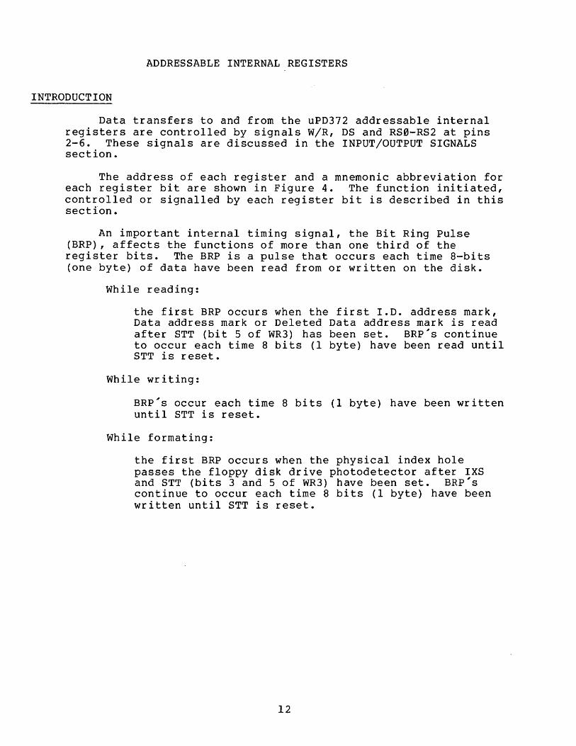
ADDRESSABLE INTERNAL REGISTERS
INTRODUCTION
Data transfers to and from the uPD372 addressable internal registers are controlled by signals W/R, DS and RS~-RS2 at pins 2-6. These signals are discussed in the INPUT/OUTPUT SIGNALS section.
The address of each register and a mnemonic abbreviation for each register bit are shown in Figure 4. The function initiated, controlled or signalled by each register bit is described in this section.
An important internal timing signal, the Bit Ring Pulse (BRP), affects the functions of more than one third of the register bits. The BRP is a pulse that occurs each time a-bits (one byte) of data have been read from or written on the disk.
While reading:
the first BRP occurs when the first I.D. address mark, Data address mark or Deleted Data address mark is read after STT (bit 5 of WR3) has been set. BRP's continue to occur each time a bits (1 byte) have been read until STT is reset.
While writing:
BRP's occur each time a bits (1 byte) have been written until STT is reset.
While formating:
the first BRP occurs when the physical index hole passes the floppy disk drive photodetector after IXS and STT (bits 3 and 5 of WR3) have been set. BRP's continue to occur each time a bits (1 byte) have been written until STT is reset.
12

REGISTER ADDRESS
W/R RS0
0 0 0
0 0
0 0
0
0 0
o
0 0 0 0
0 0 0
0 0 0
REGISTER NAME
WRITE
WR0
WRl
7
REGISTERS
RST I Mel I X
CBS X CB5
BIT NUMBERS
o
X I HlD I LCT I WFR I X I CB4 CB3 UAS UAl UA01
WR2 I WD7 I WOO I WD5 IWD4 I WD31 WD2 I WDI I WD01
WR3 RCS I WCS STT I WES I IXS I WER
WR4 STS SID SOS X
I X I UBS
WR6
READ REGISTERS
RR0 AlH I RYB UBl UB0 ERR I TRO
RRl I WRT I T00 OER COR I RYA I WFT
RR2 I R07 R06 R05 RD41 R03 R02
X=NOT USED
FIGURE 4 ADDRESSABLE INTERNAL REGISTERS
13
CCG CCW I
UBl UB01
IRQ I ORO
UAl I UA0
R01 I RD01

WRITE REGISTERS
write Register 0 (WR0)
WR0-Bit 0 Not Used.
WR0-Bit 1 WFR (Write Fault Reset)
A logic one transmitted to bit 1 sets the output of WFR pin 23 to a logic one. The one logic level remains at pin 23 until a logic zero is transmitted to bit 1. The signal at pin 23 may be used for any command purpose, but normally is used to reset a Write Fault condition.
To reset Write Fault, a logic one is transmitted to bit 1 and about 10us later a logic zero is transmitted to bit 1. This forms an approximately 10us wide pulse at pin 23 - the width specified by most disk drive manufacturers.
A Write Fault is signaled by a drive whenever an attempt is made to turn on the write current illegally (viz. when the head is not loaded). The Write Fault condition is sensed by the processor in bit 2 of RRI.
The status of LCT and HLD, bits 2 and 3 of WR0 should be preserved during Write Fault Reset commands. See note after bit 7 of WR0.
WR0-Bit 2 LCT (Low Current)
IBM floppy disk specifications define two values of write current. The higher value is to be used when writing on the outer tracks (00-43) and the lower value is to be used on the inner (higher density) tracks (44-76).
Pin 22, LCT, of the uPD372 should be connected to the floppy disk drive's Low Current input control line. A logic zero in bit 2 sets a flip-flop to the high current state; a logic one sets the flip-flop to the low current state. The output of the flip-flop is connected to pin 22.
During the SEEK routine LCT should be set to a one when the software ~rack counter becomes greater than 43. It should be set to zero when the counter becomes less than or equal to 43.
The state of HLD, bit 3, WR0 should be preserved during Low Current commands. See note after bit 7 of WR0.
WR0-Bit 3 HLD (Head Load)
14

A logic one at the HLD bit sets the Head Load flip-flop. A logic zero resets the flip-flop. The Q output of the Head Load flip-flop is internally connected to pin 19, HLD. Pin 19 should be connected to the floppy disk drive HEAD LOAD input control line.
The head requires a settling time (approx. 40ms -- see drive specifications) after loading the head and before reading or writing begins.
The state of LCT, bit 2, WR0 should be preserved during Head Load commands. See the note after bit 7 of WR0.
WR0-Bit 4 Not Used.
WR0-Bit 5 Not used.
WR0-Bit 6 MBL (Must Be Low)
This bit must be a logic zero during each command to WR0.
WR0-Bit 7 RST (Reset)
A logic one transmitted to bit 7 resets the uPD372. The effect is exactly the same as that of a pulse on pin 1.
All bits in all write registers; all bits in the read data register, RR2; all disk drive command signals; and Write Data (pin 18) are set to a logic zero.
NOTE: Commands are made to individual bits in WR0. However, every WR0 bit is affected by any data transfer to WR0. For instance, to load the head of the selected drive, HLD is set to a one, but what should the other bits of the command be? RST, MBL and WFR should be zero. Bits 0, 4 and 5 may be anything but the LCT status of the selected drive should be left unchanged. Consequently, a software image of HLD and LCT must be maintained for each drive. Whenever HLD, LCT or WFR is addressed, the selected drive HLD and LeT status must be recalled and incorporated in the command data transfer. This is accomplished by the WR0 MANAGER subroutine in the software listing for the FLOPPY DISK CONTROLLER EXAMPLE given in this manual.
Write Register 1 (WRl)
WRI-Bit 0 UA0 (Unit A0 Set)
15

WRI-Bit 1 UAI (Unit Al Set)
WRI-Bit 2 UAS (Unit A Strobe)
Bit 0 (UA0) and bit 1 (UAI) control the logic levels of output pins 30 (UA0) and 29 (UAI) respectively. These logic levels may be used for any command function. The logic levels at pins 30 and 29, along with these at pins 28 and 27 (see WR4 bits 0, 1 and 2 -- UB0, UBI and UB5) could simply be the select signals for four disk drives. Or, in a more sophisticated system, UA0 and UAI can select one of up to four drives for a read or write operation and UB0 and UBI can select another of the drives for a simultaneous track seek operation.
If bit 2, UAS is a logic zero when addressing WRl, the logic levels at pins 30 and 29 remain unchanged regardless of the content of bits 0 and 1. If bit 2 is a logic one when addressing WRI, the logic levels at pins 30 and 29 are set to the logic levels of bits 0 and 1. This allows the write clock bits (bits 3, 4, 5 and 7 of WRI) to be addressed independently from the Unit A select bits.
WRI-Bit 3 CB3 (Write Clock Bit 3)
WRI-Bit 4 CB4 (Write Clock Bit 4)
WRI-Bit 5 CBS (Write Clock Bit 5)
WRI-Bit 6 (Not Used)
WRI-Bit 7 CBS (Write Clock Bit Strobe)
IBM specifications include definitions of four special byte code patterns termed "address marks". See the INTRODUCTION of the DATA CONDITIONER section for a discussion of code patterns and address marks. What distinguishes the address marks from other bytes sent to or read from the disk is that some of the "clock" pulses are missing.
The clock pattern for ID address marks, Data address marks and Deleted Data address marks is a C7 (hex). The clock pattern for the Index address mark is D7 (hex). Since all clock pulses are present for every other byte (gap or data byte) the clock pattern is FF (hex).
For all three clock patterns bits 0, 1, 2, 6 and 7 must be logic ones. Only bits 3, 4 and 5 may be zeros. During writing the uPD372 allows the state of clock bits 3, 4 and 5 to be
16

controlled by CB3, CB4 and CBS. The other clock bits are always logic ones.
In order to change the state of CB3, CB4 or CBS, CBS must be a logic one. If CBS is a zero, CB3, CB4 and CBS are unaffected by data transfers into WRI.
To set an FF (hex) clock pattern for data and gap bytes, B8 (hex) should be written into WRI. To set a C7 (hex) clock pattern for 10, Data or Deleted Data address marks, 80 (hex) should be written into WRI. To set a D7 (hex) clock pattern for Index address marks, 90 (hex) should be written into WRI.
Write Register 2 (WR2)
WR2-Bits 0-7 WD0-WD7 (Write Data Register)
When the uPD372 is writing on the disk, the data from WR2 and the clock pattern from WRI are transferred to a l6-bit shift register once every 16 Write Clock (WCK) cycles. The data and clock bits are frequency modulation encoded and serially transmitted from the shift register through pin 18, WD (Write Data) to the selected floppy disk drive read/write head.
If the processor does not transfer new data to WR2, the write data pattern in WR2 remains constant and is repeatedly written on the disk.
Write Register 3 (WR3)
WR3-Bit 0 CCW (Cyclic Check Words)
CCW must be set to a one while the floppy disk drive read/write head is either reading or writing the last data byte of an ID or data record. It must be reset to a zero while the head is reading or writing the second CRC byte. See program listings for READ ID, READ DATA and WRITE DATA for exact sequence.
In the Read Mode, the Bit Ring Pulse (BRP) which follows the setting of CCW begins a bit-by-bit serial comparison between the CRC bytes read from the disk and the CRC bytes generated and stored in the uPD372 CRC register. The comparison ends at the time of the BRP which follows the resetting of CCW. The same BRP sets bit S of RRI (DER-Data Error) to a one if an error was detected. DER is set to a zero if no error was detected. The DER information remains valid for one byte time (while the head is reading the first gap byte following the record).
In the write mode, CCW is used to write the two CRC bytes. The BRP which follows the setting of CCW causes write data to be
17

taken from the CRC register rather than the write data register, WR2. The writing of the CRC bytes ends at the time of the BRP following the resetting of CCW. See program listing for WRITE DATA.
WR3-Bit 1 CCG (Write Cyclic Check Generator Start)
CCG is used only in the write mode to start the calculation of the CRC. (CRC calculation begins automatically at the address mark in the read mode.) CCG must be set to a one while the head is writing the last gap byte before writing an ID or Data record. CRC calculation begins at the time of any BRP which occurs while CCG is a one. Consequently, CCG must be reset to a zero while the head is writing the first byte (address mark) of the record or the next BRP would start the CRC calculation again. See the program listing for WRITE DATA for the exact sequence.
WR3-Bit 2 WER (Write Enable Reset)
See Bit 4 of WR3 (Write Enable Set--WES)
WR3-Bit 3 IXS (Index Start)
IXS is used in conjunction with STT to start the formatting routine at the physical index. See STT, bit 5 of WR3.
WR3-Bit 4 WES (Write Enable Set)
A logic one at WES sets and a logic one at WER resets a flip-flop. The Q output of this flip-flop is synchronized with the BRP to set the write Enable flip-flop. The Q output of the write Enable flip-flop is connected to pin 24, WE. The signal on this pin should be used to enable the write current of the selected floppy disk drive.
WR3-Bit 5 STT (Start)
STT starts and ends every read, write and format operation.
Reading:
An A0 (hex) is transmitted to WR3 (STT and RCS=l). The next ID address mark, Data address mark or Deleted Data address mark read by the disk drive causes an interrupt request and a BRP. Interrupts continue to occur as each byte is read and at each physical index until STT is reset.
18

Writing:
Each write operation is preceded by a READ ID routine (which STT starts). STT remains a logic one during READ ID, during the gap between the ID record and the data record and while writing a new data record. STT is not reset until the data record has been written.
The clock source is switched to the Write Clock and write current is enabled 11 bytes (in IBM format) after the ID record. Writing begins at the next BRP. Six new gap bytes are written, the data record is written and one new byte in the following gap is written before STT is reset. After STT is reset, the next (and last) BRP resets the write current.
BRP's and interrupt requests occur at each byte from the start of READ ID until STT is reset at the end of WRITE DATA. See listing of WRITE DATA.
Formatting:
A 78 (hex) is transmitted to WR3 (STT, WCS, WES and IXS = 1). The next physical index signal (IDS pin 7) enables the write current and starts a series of BRP's and interrupt requests. These continue for one entire disk revolution while the track is being formatted with data bytes, gap bytes and address marks provided by the processor. STT is reset at the next index request flag (IRQ bit 1 of RR0) ending the BRP's and interrupt requests and turning off the write current. See the listing of the FORMAT routine.
Resetting STT automatically resets Write Enable, sets WCS (Write Clock Set) and prevents further data requests (DRQ) and index requests (IRQ). See program listings of READ ID, READ DATA and WRITE DATA for examples of the use of STT.
WR3-Bit 6 WCS (Write Clock Set)
WR3-Bit 7 RCS (Read Clock Set)
WCS and RCS do not enable write current nor do they determine whether the uPD372 is in the write mode or the read mode; they simply select one of two sources of clock signals for the internal timing of the uPD372. The two clock sources are WCK (Write Clock-pin 13) and RCK (Read Clock-pin 10). Both signals have a frequency of 500KHz (2usec period) for IBM format. WCK should be derived from a crystal controlled oscillator. RCK must be derived from and synchronized with data and clock pulses read from a disk. This is accomplished by the DATA CONDITIONER circuit. See DATA CONDITIONER section.
19
The Read Clock is used only when STT is set and data is being read from the disk. The Write Clock is the normal clock source. The timing source is switched from the Read Clock to the Write Clock by any of the fOllowing.
1. By the BRP following the setting of WCS.
2. By resetting STT
3. By RST
The logic level of CKS (Clock Status) pin 15 is set high by any of the above.
The source of timing signals is switched from WCK to RCK by setting RCS. The logic level of CKS is set low by RCS.
Write Register 4 (WR4)
WR4-Bit 0 UB0 (Unit B0 Select)
WR4-Bit I UBI (Unit Bl Select)
WR4-Bit 2 UBS (Unit B Strobe)
Bit 0 (UB0) and bit 1 (UBI) control the logic levels of output pins 28 (UB0) and 27 (UBI) respectively. These logic levels may be used for any command function. The logic levels at pins 28 and 27, along with those at pins 30 and 29 (see WRI bits 0, I and 2--UA0, UAI and UAS) could simply be the select signals for four disk drives. Or, in a more sophisticated system, UA0 and UAI can select one of up to four drives for a read or write operation and UB0 and UBI can select another of the drives for a simultaneous track seek operation.
If bit 2, UBS is a logic zero when addressing WR4, the logic levels at pins 28 and 27 remain unchanged regardless of the content of bits 0 and 1. If bit 2 is a logic one when addressing WR4, the logic levels at pins 28 and 27 are set to the logic levels of bits 0 and 1. This allows the step bits (bits 5, 6 and 7 of WR4) to be addressed independently from the unit B select bits.
WR4-Bit 3 Not used
WR4-Bit 4 Not used
20

WR4-Bit 5 SOS (Step Out or Step)
WR4-Bit 6 SID (Step In or Direction)
WR4-Bit 7 STS (Step Strobe)
Bits 5 (SOS) and 6 (SID) control the logic levels of output pins 26 (SOS) and 25 (SID) respectively. These logic levels may be used for any command function but are normally used to form stepping pulses to move the read/write head of the selected drive.
The step pulse width, repetition rate and the direction control scheme vary from one drive to another. The uPD372 can adapt to any drive with software changes only. For instance, many drives require a DIRECTION logic level to determine which direction (in or out) the read/write head is to move and a STEP pulse to trigger the actual movement. For these drives uPD372 pin 25 is connected to the drive DIRECTION input and pin 26 to the STEP input. To move the read/write head, DIRECTION is set with bit 6 and STEP is set to a one with bit 5. One pulse width later (usually about 10usec) STEP is set to a zero with bit 5. One repetition period later (usually about 10msec) STEP is again set to a one with bit 5. One pulse width later STEP is set to a zero again. This process continues until the read/write head arrives at the correct track.
The timing of the repetition rate is facilitated by the 1.024msec timer provided by the uPD372. See RR0-Bit 2, TRQ (Timer Request).
Other drives require STEP IN pulses on one input line and STEP OUT pulses on another. For these drives uPD372 pin 25 is connected to the drive STEP IN input and pin 26 is connected to the drive STEP OUT input. STEP IN or STEP OUT pulses are formed under program control in a manner similar to that described above.
If bit 7, STS (Step Strobe) is a logic zero when addressing WR4, the logic levels at pins 26 and 25 remain unchanged regardless of the content of bits 5 and 6. If bit 7 is a logic one when addressing WR4, the logic levels of pins 26 and 25 are set to the logic levels of bits 5 and 6. This allows the unit select bits (bits 0, 1 and 2 of WR4) to be addressed independently from the step bits.
Write Register 5 (WR5) Not used.
write Register 6 (WR6)
21
WR6-Bit 0 DRR (Data Request Reset)
A logic one transmitted to DRR resets the Data Request, DRQ. See DRQ bit 0 of RR0.
WR6-Bit 1 IRR (Index Request Reset)
A logic one transmitted to IRR resets the Index Request (IRQ). See. IRQ bit 1 of RR0 •.
WR6-Bit 2 TRR (Timer Request Reset)
A logic one transmitted to TRR resets the Timer Request (TRQ). See TRQ bit 2 of RR0.
WR6-Bit 3-Bit 7 Not Used.
READ REGISTERS
Read Register 0 (RR0)
RR0-Bit 0 DRQ (Data Request)
When DRQ is true, the processor controlling the uPD372 should read a data byte from RR2 during the read mode or transmit a data byte to WR2 during the write mode.
DRQ causes an Interrupt Request (REQ) at pin 17.
DRQ's are generated as follows:
1. During the read mode the first ID address mark, Data . address mark or Deleted Data address mark (but not Index address mark) which is read following the setting of STT (bit 5-WR3) sets DRQ. From this point on, DRQ is set again by every BRP (i.e., after every byte--data byte, gap byte or address mark--is read) until STT is reset. DRQ must be reset, by DRR (Data Request Reset--bit 0, WR6) each time that it is set. If DRQ is still true at the time of the following BRP, a Command Overrun Error results (signaled by COR--bit 4, RRl). DRQ is automatically reset when STT is reset.
2. During the write mode Data Requests occur at each BRP (i.e., after each byte--data byte, gap byte or address mark--is written). As in (1) above, DRQ must be reset each time that it is set or a Command Overrun Error results.
22
3. During formatting a series of DRQ's begins when the physical index hole is detected after setting STT and IXS (bits 3 and 5 of WR3). The DRQ's continue to occur at every BRP until STT is reset. (STT and IXS should be reset at the end of one complete revolution--when IRQ, Index Request, bit 2, RR6 becomes true.)
RR0-Bit 1 IRQ (Index Request)
IRQ is set true by the leading edge of the physical index pulse. The physical index pulse is generated when the index hole of the floppy disk passes a photo detector in the disk drive. STT must be set to enable IRQ.
IRQ causes an Interrupt Request (REQ--pin 17).
IRQ is reset by transmitting a logic one to IRR (Index Request Reset--bit 1, WR6) , by resetting STT and by RST.
RR0-Bit 2 TRQ (Timer Request)
TRQ is the Q output of a flip-flop which is set by every 5l2th Write Clock (WCK, pin 13) pulse. The Write Clock period for IBM compatible controllers is 2us causing TRQ to be set every 1.024msec. TRQ is set every 2.048msec when using Shugart Minifloppy format.
TRQ does not cause an Interrupt Request (REQ, pin 17).
TRQ is reset by transmitting a logic one to TRR (Timer Request Reset--bit 2, WR6) and by RST.
RR0-Bit 3 ERR (Error)
ERR indicates a condition that must be corrected before issuing a command to the disk drive. ERR is the logical OR of three status signals:
ERR = WFT + RYA + COR
where: WFT is Write Fault--bit 2, RRl
RYA is Disk Drive A Ready--bit 3, RRl
COR is Command Overrun--bit 4, RRI
RYB is not involved in the calculation of ERR.
23

RR0-Bit 4 UB0 (Drive B0 Selected)
RR0-Bit 5 UBI (Drive Bl Selected)
UB0 and UBI are two of the four status bits (the other being bits 0 and 1 of RRl) that indicate which disk drive has been selected. See descriptions of bits 0, 1 and 2 of WR4 and pins 27 and 28.
RR0-Bit 6 RYB (Drive BReady)
This status bit indicates the logic level of RYB at pin 14. Pin 14 is usually connected to the READY output of the drive selected by UB0 and UBI (bits 0 and 1 of WR4).
RR0-Bit 7 ALH (Always High)
This bit is a logic one as long as power is supplied to the uPD372.
Read Register 1 (RRl)
RRI-Bit 0 UA0 (Drive A0 Selected)
RRI-Bit 1 UAI (Drive Al Selected)
UA0 and UAI are two of the four status bits (the other being bits 4 and 5 of RR0) that indicate which disk drive has been selected. See descriptions of bits 0, 1 and 2 of WRI and pins 29 and 30.
RRI-Bit 2 WFT (Write Fault)
This status bit indicates the logic level of WFT, pin 8. Pin 8 is usually connected to the WRITE FAULT output of the selected drive. A write fault condition occurs when a floppy disk drive detects an illegal command during a write operation. All commands to that drive are ignored as long as the write fault condition exists. The write fault is reset by WFR, bit 1, WR0.
RRI-Bit 3 RYA (Drive A Ready)
This status bit indicates the logic level of RYA at input pin 12. Pin 12 is usually connected to the READY output of the drive selected by UA0 and UAI (bits 0 and 1 of WRl).
24

RRl-Bit 4 COR (Command Overrun)
COR indicates that the processor did not respond in time to a Data Request (DRQ) during either a read or a write operation. See DRQ, bit 0 of RR0.
RRl-Bit 5 DER (Data Error)
DER indicates that a CRC error occurred during a read operation. DER is explained in detail in the description of CCW (Cyclic Check Words) bit 0 of WR3.
RRl-Bit 6 T00 (Track Zero)
This status bit indicates the logic level of T00 at input pin 9. Pin 9 is usually connected to the TRACK 00 output of the selected disk drive. The disk drive places a high logic level on TRACK 00 when and only when the read/write head is at track zero.
RRl-Bit 7 WRT (Write Mode)
WRT indicates which clock signals the uPD372 is using for internal timing--Write Clock (WCK, pin 13) or Read Clock (RCK, pin 10). The selection is made by WCS (Write Clock Select) or RCS (Read Clock Select) bits 6 and 7 of WR3.
The logic level of WRT is identical to the logic level of CKS, output pin 15.
Read Register 2 (RR2)
RR2-Bits 0-7 RD0-RD7 (Read Data Register)
Data, serially read from the selected disk drive, is assembled into 8-bit parallel bytes in an internal shift register and is then transferred to RR2 at each BRP. See READ ID and READ RECORD routines for examples of the use of the Read Data Register.
25

DATA CONDITIONER
INTRODUCTION
Frequency modulation encoded data as transmitted to or received from a floppy disk drive consists of a series of timing or "clock" pulses interleaved with a series of data pulses (see Figure 5). The period between successive clock pulses is termed a "data cell". The presence of a data pulse within a data cell represents a logic one data bit. The absence of a data pulse within a data cell represents a logic zero data bit.
The clock pulses also contain information. Just as with the data pulses the presence of a clock pulse within a data cell represents a logic one clock bit. And, the absence of a clock pulse within a data cell represents a logic zero clock bit. Each byte is made up of eight data bits and eight clock bits for a total of sixteen.
Since the data read from a floppy disk is in serial format, the controller must have some means of distinguishing between clock bits and data bits and must also be able to determine the beginning of each byte. To provide this synchronization, soft-sectored floppy disks are written with a special byte, an address mark, at the beginning of every record.
All bytes, except address marks, contain the full complement of eight clock pulses for a clock pattern of FF (hex). In IBM format the address marks written at the beginning of records (ID Address Mark, Data Address Mark and Deleted Data Address Mark) each have a C7 (hex) or 11000111 (binary) clock pattern.
The data pattern for an ID address mark is FE (hex) or 11111110 (binary), for a Data address mark is FB (hex) or 11111011 (binary) and for a Deleted Data address mark is F8 (hex) or 11111000 (binary).
The generalized sixteen bit (interleaved clock and data) pattern for these address marks takes the form:
lll10l0l0llAlBlC (binary)
where at least one of the numbers, A, B or C is a zero.
This pattern cannot be generated by any sixteen bit sequence read from a floppy disk except those of an address mark. All other sixteen bit sequences must have a logic one in alternate locations to represent an FF (hex) clock pattern.
26

CLOCK DATA CLOCK DATA CLOCK DATA CLOCK
LCELLI • 1. CELL2 .1 • CELL3~ LOGIC 1 LOGIC 0 LOGIC 1
FIGURE 5 FLOPPY DISK DRIVE SERIAL DATA FORMAT
r ~Tcy+160ns T ~Tcy+160ns 1 RCK -.J I r RD ) RD MUST BE STABLE (
~Tcy-150ns L I 14----~2Tcy+l00ns ----J
Tcy = 01 CYCLE TI ME
FIGURE 6 READ CLOCK (RCK) AND READ DATA (RD) REQUIRED BY uPD372
RAW WRITE SIGNAL -U (CLOCK AND DATA)
iii' I I I I
2.0us ----.. f IL._J 14----------- 4.0us --------------I.~ I:
FIGURE 7 IBM FORMAT WRITE DATA TRANSMITTED TO DRIVE
l r~200nS
RAW READ SIGNAL --, I I I I I L.J I I I I
(CLOCK AND DATA) I ... :f----- 1.8us-2.4us ___ -., .... r-J
IL-.J
101·-1----------- 3.4us-4.6us ----------t .. ~
FIGURE 8 SAME DATA READ BACK (TRACK 76)
27

Each bit (clock and data) received by the uPD372 from a floppy disk drive is clocked into a sixteen bit shift register. Once STT (bit 5 of register WR3) is set to a one, the uPD372 begins looking for the address mark pattern in the shift register. When the address mark pattern is found, a BRP (Bit Ring Pulse) is formed, the eight data bits in the shift register are transferred into the Read Register (RR2) and the Data Request flag is raised. From that point until STT is reset, every sixteenth bit clocked into the shift register causes a BRP and a Data Request and transfers the data bits to the Read Register.
Signals Required by the uPD372
In order to clock a bit into the uPD372 shift register, the desired logic level, zero or one, must be maintained at the READ DATA input (RD, pin 11) and a positive going transition must be made at the READ CLOCK input (RCK, pin 10).
The uPD372 samples RCK with the trailing edge of 02. Since RCK is asynchronous with 02, there is an uncertainty of one 02 clock cycle, Tcy, in the time when the uPD372 senses the positive going edge of RCK. Furthermore, RCK is not sampled instantaneously -- a setup time and hold time are required. Consequently, after RCK goes high, it must remain high for at least Tcy + 160ns to guarantee that the positive transition is sensed. For the same reason, after RCK returns to the low state, it must remain low for Tcy + l60ns before the next positive transition.
Once a positive transition of RCK is sensed by 02, the following 02 clocks the logic level at RD into the shift register. -So, the earliest time that RD can be clocked is nearly Tcy after the positive transition of RCK and the latest time is about 2 Tcy after the positive transition of RCK. RD must be stable during this period and for a short time before and after.
The timing requirements of RCK and RD are summarized in Figure 6.
Most floppy disk controllers require that the data pulses read from a drive be separated from the clock pulses by an external "DATA SEPARATOR" circuit. The uPD372, on the other hand, reads the combined clock and data information and separates the data internally. So, it does not require an external DATA SEPARATOR.
The uPD372 does, however, require some modification of the raw data read from the disk. The modification is accomplished by a circuit termed a "DATA CONDITIONER".
28

Data Conditioner Algorithm
The function of the DATA CONDITIONER is to translate the pulses of the raw data, read from a disk, into the RD and RCK signals required by the uPD372. Except for an amendment, which for the sake of clarity is introduced later, the DATA CONDITIONER performs the translation by using the following algorithm:
1. Each time a raw data pulse (clock or data) is received from a floppy disk drive, the DATA CONDITIONER sets the uPD372 RD input to a logic one and sends a positive pulse to the RCK input. The RD and RCK signals must meet the requirements of Figure 6. In addition, the receipt of a raw data pulse starts an interval timer with a period of 1.4T--where T is the average time between adjacent clock and data pulses. In other words, T is the approximate time before the next raw data pulse will arrive, if it is present. GO TO 2. or 3.
2. If the next raw data pulse arrives before 1.4T, the DATA CONDITIONER continues to maintain a logic one at RD, generates another RCK pulse and restarts the interval timer. GO TO 2. or 3.
3. If no raw data pulse has arrived by 1.4T, the pulse is declared absent. The DATA CONDITIONER sets the RD input to a logic zero and generates another RCK pulse. The interval timer is not reset until the next raw data pulse is received. GO TO 1.
An amendment must be made to the above algorithm in order to guarantee that the requirements of Figure 6 are always satisfied. Once RCK goes high, it must remain high for a least Tcy + 160ns before going low. Once low, it must remain low for at least Tcy + 160ns before going high. The minimum RCK cycle time is, therefore, 2Tcy + 320ns. For the normal Tcy of 500ns the minimum RCK cycle time is 1320ns. This presents no problem in the long run because the average time between adjacent raw data pulses (in IBM format) is 2us, but it does present a problem between any two closely spaced pulses.
Figure 7 shows the regularly spaced raw write data sent to a floppy disk drive and Figure 8 shows the timing variations in the same data read back from the drive. A decision that the second pulse is missing in Figure 8 cannot be made until 2.8us after the first pulse (T = 2us in IBM format). If a RCK cycle is begun at 2.8us, it cannot be completed for another 1320ns or not until 4.12us after the first pulse; but, the third pulse may occur as early as 3.4us. Obviously, in order to meet the requirements of Figure 6, the DATA CONDITIONER must be capable of storing the information about one raw data pulse while completing the RCK cycle of another.
29

To meet this requirement the first sentence of the algorithm must be amended as follows:
1 •. Each time a raw data pulse (clock or data) is received from a floppy disk drive, the DATA CONDITIONER waits until the previous RCK cycle is completed and then sets the uPD372 RD input to a logic one and sends a positive pulse to the RCK input.
DATA CONDITIONER EXAMPLE
A DATA CONDITIONER which uses the above algorithm and with one-shot times set for IBM format is shown in Figure 9 along with a timing diagram. Tcy, the 02 cycle time, is assumed to be 500ns.
Raw data consisting of clock and data pulses is shown in the top line of the timing diagram. The first pulse occurs at time zero. The second pulse is missing indicating a logic zero. The third pulse is early by 600ns. The fourth pulse occurs at the expected time. This pattern is the worst case because of the short time interval between the decision that the second pulse is missing and the early third pulse.
One-shot U31A generates the 1.4T time interval. Flip-flop U29A stores the information that a RCK cycle should begin when possible. One-shot U31B prevents the start of a RCK cycle until the previous cycle is completed. Flip-flop U298 double buffers the raw data. One-shot U30B forms RCK.
Other Formats and Other 02 Cycle Times
The same DATA CONDITIONER will operate with formats other than IBM and with 02 cycle times othe~ than 500ns.
When using other formats the only parameter which affects the DATA CONDITIONER is the read data transfer rate and the only one-shot affected is the 1.4T time interval one-shot, U31A. The period of U31A should be 1.4T for all T. For example: T=2us in IBM Format so the period of U31A should be 2.8us and T=4us for the Shugart Minifloppy so the period of U31A should be 5.6us.
When using other 02 define RCK are affected. period of U30B should be should be 2 Tcy + 500 ns Figure 6.
cycle times, the two one-shots which If the 02 cycle time is Tcy, then the
Tcy + 250 ns and the period of U31B in order to keep RCK consistent with
30

0 Ius
I I RAW DATA 0 LJ
---I @ I __ ..J
@
@LJ @ ---1l
® --1l
® -U @
RCK 0 I I
RD o --- :-u ---~ j350nS
) MUST BE STABLE ) ( 1100 ns--l
RAW DATA
NOTES
PICK TO
TRIM
I. 01 CYCLE TIME, TCY = 500ns 2. FORMAT IS IBM 3740
+5V
9.IK METAL FILM
FROM FLOPPY -<l:)o-~HII,..,.o"""....;.a DISC DRIVE
2us
I MISSING
• • , • 1._.1
3us 4us 5us 6us
I EARLY I I I U i· U---, .
"."
U
U U U--
n L-
n n rL
U U u-U LJ
I
t
) ( ) (
r-________________________ ~II RD
+5V uPD372
10K ~----------~IO~RCK
UP2 +5V
+5V 5.IK
5.IK
UPl
FIGURE 9 DATA CONDITIONER EXAMPLE AND TIMING DIAGRAM
31
FLOPPY DISK CONTROLLER EXAMPLE
HARDWARE
Figure 10 is divided into two sections. The section on the right shows a floppy disk controller which may be interfaced either directly to a host processor or indirectly through a controller processor. The section on the left shows a controller microprocessor system. Both the host and the controller processors are uPD8080A's in this example and the single floppy disk drive is IBM3740 compatible.
The controllet and host processors share a common memory. lK bytes of ROM is accessed by the controller processor between 0000-03FF of its address space. The same ROM is accessed by the host processor between E000-E3FF of its address space. 256 bytes of RAM is accessed by the controller processor between 0400-04FF of its address space. The same RAM is accessed by the host processor between E400-E4FF of its address space. The ROM stores the Disk Handling Routines and the RAM provides temporary storage for data, commands, status, etc.
The controller processor system configuration shown in Figure 10 is a testbed for software and hardware changes in the floppy disk interface. The intent is to give the host processor (which is assumed to have an editor and a console) the ability to monitor the performance of the controller processor and the rest of the floppy disk interface. Consequently, the direction of Direct Memory Access is from the host into the controller rather than vice versa and no provision is made to allow the controller to interrupt the host.
An interrupt feature would require the addition of only two chips. The resulting controller would be satisfactory for many applications although the host would have to transfer data between the common RAM and the desired storage locations. A circuit which allows Direct Memory Access from the controller into the host would require several logic changes resulting in a net gain of a few chips.
Circuit Description
The circuitry to the right of the uPD372 in Figure 10 contains the line drivers and receivers for the floppy disk drive. One shot U26B "stretches" the 60-l00ns wide Write Data (WD) pulses into the width specified by the drive manufacturer.
The logic below the uPD372 is the Data Conditioner which is described in the DATA CONDITIONER section.
32

U:34 74157
C-HLDA
H-MEMW B
b-------=.dlA Ul ~~~1-------~L-J
n:: o IU w 2 Z o U
W ~ Cl W
Cl n:: ct u n:: w I:::> a. :E o U
Ien o ::I:
200Pf T ,...,.SOns DELAY rh C-MEMW-------'<IIB NOTE 4 __ _
H- DB I N »----"'<l2A H-MEMR -"""",-_.J
C-MEMR-------~2B
C-HOLD·C-HLDA-------~
DB7 OB6 DB5 DB4 DB3 DB2 OBI DB0
DB7 DB6 DB5 DB4 DB3 DB2 OBI DB0
U2
A9 A8 A7 A6 A5 A4 A3 A2 Al A0
A9 A8 A7 A6 AS A4 A3 A2 Al A0
UP3
DB7
DB6
U3 OB5
OB4
A7 A6
A5 S A5 A4 21 A4 A3 A3 A2 A2 Al Al A0 4 A0
VCC 22
DB3
DB2
OBI
DB0
NOTES 182 74365 PROM uPD458
uPD2308 ROM BYTES
uPD21 0 IAl-4 RAM 256 BYTES
15 G2
r----. H-AIOt---------------=2--tlA U5 H-A9~-----------------~:~2A lY~~--------------------------------_, H-A8 3A 2Y~----------------------------------------------_t. H-A7 10 4A ~ 3Y 7 H-AS 12 5A ~ 4Y~~---------------------------------------------------------ri_t~
5Y~II---------------------------------ri_t_r,
-t----L<Gi ----.. 74365
U6
UP3
17 19 18 20
CE2 CEI 00 R/W 15 014 A7 7 A7 16 004 A6 6 A6 13 013 A5 5 A5 14 003 A4 21 A4 II 012 U4 A3 I A3 12 D02 A2 2 A2 9 011 Al 3 Al
10 001 A0 4 A0 8 GNO VCC 22
uPD2101Al-4 RAM
....... r----:!:< GI r ~G2
H-A5J------------------------~-~lA
~U 4~ H-A3 6 3A H-A2 10 4A
IY 3 2y~5------------------------------------------------~_t~t_r; 3Y~7-----------------------------------------_r+_~rt_r+l 4Y~9--------------------------------~rt_+_r+_~rt, 5Y II
H-AI ·12 5A 6Y 13
H-A0 14 6A uPD8080A
I UI7
.~ H-REAOY I ~~O.~c~. -------------------,
H-Al51-------,
H-AI41------t
H-AI31--------....
H-AL2 A-....?404 ~ H-(EOOO-E7FFl ~~404 7430;~·~~~~~~~-----t_---r_----_,
H-Al1 ... " I ..... .,
H-ClJIJ~:C~ 6.SK 20~Pf
H-SYNC.FU22 ~: ~5~bf;!sonJ~a 0 sao S a C-HOL~:3 HOLD
NOTE 3 '1 )C >C
I. C_HUL~~ j] Q m! R Q m~ Q ~ +12V V m+~
I UPI SYSRST SYSRST ~ -5V
I uPB8224 01 RESET 02 - GND I SYSRSf~ RESi1il RESET I 12 RESET
H-SYSRST" ~r-SYSRST I:15 XTALI SY~i 51'01 1. ..1 2115~ ~iNC IU2374125 02 4 ~ 02
'~., ~ +5V RDYIN~432'-- WAIT
INT~ INT
U8 AIO ~S A10 A9~~--------------------------__ ~-r+-~-r1-r_-------A9 ~M ~ A7 '13 A7 A6 32 A6 A5 31 A5 AA~ U ~~ ~ H ~ AI 20 Al A0 zs -A0
C-HLOA C-HLDA uPB8238 UP4 UP5 UP6 UP7 UPS _. ~;~·-C _~2~'~ BUSEN MEMW 26 1 1 1 _L C-MEMW HLOA ~ HLDA NMIEE:NMIRRII>!~~~:--------4.J.. ___ -..l+--+l--+---- C-MEMR
ViR 18 7404 7404;3· WR i~g ~ 25 g:~~g ~ DBIN 17 4 DBIN INTA 23 C-INTA
07 6 8 07 DB7~7------~--------------------OB7 06 5 21 06 DB6 20 DB6 05 4 19 05 DB5 18 OB5 04 3 6 04 U9 DB4t-::5'------_r-HH--------- DB4 D3 7 10 D3 DB3r9'---rt_r+_H~-------- DB3 D2 8 12 02 OB2t-"-'..1 ----Hrt_+++--------- OB2 01 9 17 01 OBI 16 OBI 00 10 15 00 DB0 13 DB0
INT ______________________________________ ~1~7 REQ
DB7 38 DE? Des 37 OB6 085 36 DB5 DB4 35 DB4
M3 ~ 003 002 ~2
C-I/'JR ~
OBI -[~f74125"'t------...., ..... L.---------...;3::.!2=-1 OBI U24
~A ~l
DB0 ~4125~ __ ~~-----------3~I~D80
~:,i5 r---t-----' ~ __________________ ~ ~ TI2V
UP2 74365 .l.2. +5V
~±~: UI3 .1.!... -5V .. 1Y~ ..12.. GNO ~ 3A 2Y ... 5"--____ ...
r---'" UB0.2~8~---------~U~177 ;:-r ...... >o-::°~·C"-. ---------------1 DEVICE SELECT I
7416
SID 2S ~~~6 ~ O.C. .DIRECTION
50S 26 ~!~6 O.C. • STEP
HLD 19 ~!~6 O.C. iHEAD LOAD
LCT I 22 ~~~ 6 O.C. I LOW CURRENT
WFR 23 UI8 O.C. IFILE UNSAFE 7416 IRESrT
WE 24 ~!~6 O.C. I WRITE GATE
I
wDtl"'8 _____ +_5_V~~~~.~~.~IK~..l'll .... rl~ii'IOh~~»~""0i"'t~· ---------;: WRITE DATA
U268 T 74123
[:: ~ 3Y LL 4yL-5Y ..!L.-
UI4 uPD372D
250"s :tSOns UP!
A2 ------~~~!~~~5~~----------t-~~--U~P2~------~4iRS2
Al _____ -:U:';2""5::; SQI---....... S'-IRS1
74125~ rflD
02 (TTL)-----------+----It-..... C R Q U32A 7474
UP2 NOTE 6 UP2
A0 ______ ~U~2~5~.?_---r----~.-_t_;o Sat-----~6~RS0 74 125 I-CL- C
~ R Q U328 C-I10 W ----------(\-__ -:::-\~ 7474
J7407 U20 UP2 NOTE 6 C-I/O R 740~,}---------------~3~DS C-I N TA -----------;~U;-::2;;:;0-----<lI.-,....,
C-I10 W ----------d-II;-.·::':-~'-_____________________ _'2"'1W/R C-l NTA _________ Q •• r~74_0 .... 3-r.
RESET I RESET 01 41 01 02 42 02
UPI ----L .S 2200. 330(\
UP2~ ~14 UP3~ ~1~3---------'
UP4 --1 UP5 --S ~~; =::L UP8~
12 U15 ~
RES. NETWORK ~ SPRAGUE
NO.916CI3IXSTR
PULL UP SOURCES
8 U33 !=-;:-=:=:: WFTF--------:;:74':.::00:-;4:-< b----~H_+++__I. FILE UNSAFE
RYB 14 U33 ',READY 7404
T00't~9-------------~~:~g~4-~<t~---------~~--~!TRACK00
lOX 7 U33 I. INDEX 7404
--IRAW DATA
I RCK~IO,-------------------,
02 (TTLI --------U-~-8~':~:2: ~~~--------~13:W--C-K---------R-D~~ ,ll:T ~ll:~ ""2
+5V
10K
I I I L ___ .J
+5V UP2 UP2
r------------------------------------------;D Sa
n:: ~ U W 2 2 o U
W ....J OJ ct U
W > a:: o :::£ (f)
Cl
>Q. Q.
o ....J U.
H-MEMW ~ ~ r H-MEMW B 10pf I ...2. +12V READY U34 24 READy
. XTA~ Cl -"'- GND U7 I "-..l-C-I10R H-MEMR tl----- H-MEMR r.
H - WR I H -WR IBM .Z T ClJ2(TTLl 6 02 (TTL)
~ +5V !.i. GND
i?:~'"'''' ",0. '5~:" i'l~'" CHI P LIS:...;T __ -I
QTY PART NO.
1 uPD372D H-DBINI H-OBIN L...!i. XTAL2 S'fSfB 7 I STSTB
I uPB8216 I .~ 013
H- DB7 :.---------------------------t~ 003 DB3,~13~--------------------------------------------_, DB2 10
H-OBS i ~ 012 DBI~6----------------------------------------.------_ti_t DB0'~3~--------------------------------------------------------ri_r~ • t....:..:.. 002
H- DB5 i r{ OIl
il ~ 001
H-DB4. ~ ~~: UlO
I I I
[
C-HOLO.C-HLDA
OlEN ~ U20 C-HOLD L ___ -~C;;S:r-"'III-~7400 C-HLDA
uPB8216 - T CS~ I
I A 013 H-DB3 r----------------------1~ 003
~ 012 H-DB2~-------------------------~.Jl D02
H- OBI I--------------------.rf Dr I ~ DOL
H-DB0~------------------------~~ 010 L ___ .J L.:. D00
0IENi~15~~-------H-MEMWB
Ull
DB3~13~--------------------~ DB2~10~-----------------------..J DBI~6'---------------------------DB01~3'---------------------------~
~125 ¥~~ ,.._7_4_3;i,.6~5_.,
~ G2 U12 ,-f-!:.cGI
2 lA lY 3 2Y 5
~ 2A 6 3A
1--rJ,Q. 4A 12 5A 14 6A
3Y 7
4Y ~I 5Y~--------------~
SY 13
NOTE S
,~ ~\"," GOO. ~""' UP< tj'. I UP2
I Q'l.t--_'<.....---)f7-:U-3~....,SE ~~:8 ~cS a al 1
1~-:::l-'l"" ..... ~~1 Q 220n UI6 RQ r-....... - .......... Q ..... j~ rt7 U31A T U29A IU30A y
9602 200Pf
I 7474 74123.!
~';5~~~ UPI ~d~8 ~~g~~ UP!
NOTES
,hU3IB T f.~~~ UP1 :!: 150 ..
1. THE HOST PROCESSOR AND CONTROLLER PROCESSOR ARE BOTH uPDSOBOA·S. HOST PROCESSOR SIGNALS ARE PREFIXED WITH H-. CONTROLLER PROCESSOR SIGNALS ARE PREFIXED WITH Co.
6. RS0-RSI MUST BE STABLE FROM 150ns BEFORE TO IOns AFTER THE TRAILING EDGE OF 0l.ISEE uPD372 SPECIFICATIONS) F/F U32 SYNCRONIZES RS0,RSI CHANGES WITH THE LEADING EDGE OF 02.
2. THE HOST HAS DIRECT MEMORY ACCESS INTC THE CONTROLLER-NOT VICE VERSA. 3. HOST ADDRESS SIGNALS DO NOT REACH THf. CONTROLLER MEMOR I ES UNTIL
C-HLDA IS GRANTED DURING A HOST ACCESS. THE HOST IS THEN IN A TW STATE. ONE SHOT U26A KEEPS THE H-READY LINE LOW ITO MAINTAIN ADDRESS AND DATA PATHS) FOR AT LEAST THE 450n. MEMORY ACCESS TIME.
4. iPiiF! IS ALREADY PRESENT DURING A WRITE CYCLE WHEN THE HOST ADDRESS SIGNALS REACH THE CONTROLLER MEMORIES (HOST IS IN A TW STATE AT C-HLDA). THIS OELAY CIRCUIT KEEPS THE CONTROLLER RAM R/W SIGNAL HIGH FOR
5. i~Fs ~~~~~~i~A~'1W A~I¥.~i/~~E~jDc26g~AfE~:~r~II~A;~~:UPTl ONTO THE DATA BUS DURING C-INTA.
7. UNLESS OTHERWISE SPECIFIED ALL RESISTORS 114W,:tS%
FIGURE 10 - uPD372D FLOPPY 0 I SC INTERFACE 3-11-77
33
2 uPD2101C7A-:-L-""'4"'"
1 uPD2308 1 7400 ----I 2 7404
1 7408
2 7416
7430
2 7432
4 7474
2 74123
3 74125
74157
4 74365
uPDBOBOA
2 uPBB21S
uPB8224
uPB8238
9602 RESISTOR NETWORK SPRAGUE NO. 914Cl31XSTR
34 TOTAL

Flip-flops U28A and U28B generate a 500KHz write Clock for IBM formats. The Shugart Minifloppy format requires an additional flip-flop to generate a 250KHz clock. Other formats may require other clock frequencies. In each case the period of the clock is equal to the period between adjacent clock and data pulses in the Frequency Modulated data stream.
U13, U24 and 3 gates of U25 force a 01 (hex) into WR6 during interrupt acknowledge. This causes a hardware reset of the Data Request (but not of the Index Request). See bits 0 and 1 of WR6.
The remaining chips in the right hand section of Figure 10, give a uPD8080A processor data transfer control over the uPD372 addressable internal registers.
The Direct Memory Access control logic is shown at the left of the uPD8080A in Figure 10. Flip-flops U27A and U27B are both set at the beginning of each host machine cycle in which the host addresses the common memory. Flip-flop U27B makes a HOLD request of the controller uPD8080A. Flip-flop U27A places the host uPD8080A in the WAIT state by lowering the host's READY input. When the controller uPD8080A grants the HOLD request, signified by C-HLDA, the host uPD8080A is given control over:
1) the Chip Enable, Output Disable and Read/Write inputs of the common memory by Ul;
2) the common memory address lines by U5 and U6;
3) the common memory data bus by U10 and Ull.
After one-shot U26A causes a delay equal to the memory access time, flip-flop U27A releases the host uPD8080A from the WAIT state. When the host uPD8080A has completed the machine cycle in which it addressed common memory, it issues a SYNC pulse which causes U27B to release the controller uPD8080A from the HOLD state. When C-HLDA goes low the controller processor is free to continue execution of its own programs.
There is sufficient delay before C-HLDA goes low to prevent this design from allowing two successive host machine cycles to be addressed to the common memory. The main effect is to prevent the host processor from executing programs in common memory, which is not a requirement of this design.
OR-gate U34, between the uPD8080A and the uPD8224, causes one wait state to occur in each machine cycle during which data is read from the uPD372; but does not cause a wait state in any other machine cycle. The uPD372 places read register information on the data bus 90ns (max.) after 01 - which is too late to remain within uPD8080A specifications without a wait state. A wait state is not required at any other time. In fact a wait state in every machine cycle is not allowed since it would make a uPD8080A system too slow to handle disk data transfers.
34

SOFTWARE
The software for the controller processor may be divided into catagories as follows:
Executive Routines
INITIALIZE RETURN FROM COMMAND IDLE LOOP EXECUTE COMMAND
Main Routines
READ ID READ DATA WRITE DATA FORMAT SEEK
Subroutines
STEP IN STEP OUT HEAD LOAD HEAD UNLOAD WR0 MANAGER UNIT SELECT DELAY
The Executive Routines initialize the floppy disk drive system after startup, interpret commands from the host processor and transfer control to the appropriate Main Routine. The Main Routines perform the actual disk drive operations. At the completion of a Main Routine, control is transferred back to the Executive Routines which inform the host processor of the result and then wait for the next processor command.
All of the software, including FORMAT, for a single disk drive controller may be stored in one lK x 8 ROM. Nearly 1/4 of this area is available for program expansion to allow control of up to four disk drives and for other purposes. This area is made available by storing most of FORMAT on a disk rather than in ROM.
When formatting is required, the major portion of FORMAT is recalled from a disk and stored in the controller RAM with only a minor portion permanently stored in ROM.
An introduction is given below to READ ID, READ DATA and WRITE DATA. The comments in the uPD8080A assembler listing which follows this section should be sufficient to understand the rest of the controller software.
35

Read Sector M on Track N
Before the read operation begins, the host processor writes the desired sector address in SECTR (location 403 in the listing) the desired track address in TRACK, the desired disk drive in UNIT and the sector size in SCTSZ. If no sector size is transmitted from the host, the controller program assumes a size of 128 (decimal) bytes.
The host processor initiates the read operation by writing an 01 in CMND (location 400). The controller program interprets the 01 as a read command and if the sector address, track address, drive address and sector size are within acceptable limits, control of the controller processor is transferred to READ DATA (See READ DATA in listing).
READ DATA starts by calling READ ID to find the correct sector and track.
READ ID
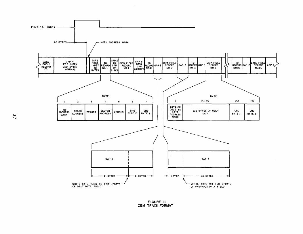
READ ID starts by calling the SEEK routine which positions the read/write head at the requested track. Next the read/write head is loaded (if it is not already loaded because of a previous operation). The read/write head then begins reading somewhere on the requested track. See IBM TRACK FORMAT Figure II. A limit is placed on the number of index holes (4) that may be counted without successfully reading the specified ID record before giving up.
The H, L registers are initialized to point to TRACK, the location containing the desired track number and the first location in the group of parameters.
The D, E registers are initialized to point to WTRK (Wrong Track) the first location in a group of error flags. uPD8080A register B is cleared and a 00 is transmitted to uPD372 write register WR3. The effect is to insure that one particular bit, bit 5, STT (Start) is at a logic zero. All the other bits of WR3 are known to be at a logic zero at this time.
An A0 is then transmitted to WR3. The effect of this command is to set STT, bit 5, and RCS (Read Clock Set) bit 7. RCS instructs the uPD372 to use read clock pulses from the disk for its internal timing control. STT instructs the uPD372 to cause an interrupt request when the next address mark passes the read/write head.
Interrupts are then enabled and the processor is halted while waiting for the interrupt.
36
w .......,J
PHY SICAL INDEX
46 BYTES INDEX ADDRESS MARK
I t DATA FIELD RECORD
26
I
~
GAP 4 GAP1
PRE INDEX POST 10
320 BYTES INDEX RECORD
NOMINAL 32 NO. t
BYTES
BYTE
4
ID TRACK SECTOR ADDRESS
ADDRESS ZEROES
ADDRESS MARK
WRITE GATE TURN ON OF NEXT DATA FIELD
I GAP2 GAP 3 to DATA FIELD 10 DATA FIELD 10 DATA FIELD ~> DATA GAP RECORD GAP RECORD GAP 2 RECORD GAP 3 RECORD GAP 2 RECORD
17 BYTES
ZEROES
NO.1 33 BYTES NO.2 NO.2
CRC BYTE 2
CRe BYTE 1
DATA OR DELETED
DATA ADDRESS
MARK
FIGURE 11 IBM TRACK FORMAT
NO.3 NO.3
BYTE
128 BYTES OF USER DATA
GAP 3
32 BYTES
'- WRITE TURN- OFF FOR UPDATE OF PREVIOUS DATA FIELD
10 RECORD NO.26
CRC BYTE 1
DATA FIELD GAP 2 RECORD
NO.26
CRC BYTE 2
I
GAP4f
I

Halt -- Interrupt Technique
The transfer rate of IBM standard floppy disks is one byte every 32us which is too fast for the usual technique of "jamming" a RST (Restart) instruction on the data bus during INTA (Interrupt Acknowledge) followed by a JMP to a service routine which ends with a RET (Return) instruction.
Instead, as shown in the READ ID routine, the processor is halted before an expected interrupt to keep the Program Counter from advancing.
When an address mark is read, an interrupt request is generated and CRC calculation automatically begins.
During INTA an EI (Enable Interrupts) instruction is jammed onto the data bus (by U12 and U23 shown in the bottom center of Figure 10) and is executed by the processor. The Program Counter is not incremented by an instruction which occurs during INTA so the next instruction executed is the one following the HLT.
Another event which occurs during each INTA is the clearing of the data request flag by U13, U24 and U25 (near the center of Figure 10) which write a 01 into WR6 (DRR-Data Request Reset).
After the address mark interrupt and the EI instruction, the READ ID routine inputs the data byte read from the disk. The data is compared with FE (hex) to determine whether or not the address mark which caused the interrupt was an ID address mark. If it was not an ID address mark, a JMP is made to the RIM subroutine which makes sure the revolution limit has not been exceeded, and then returns the Program Counter to RIA to wait for the next address mark. If it was an ID address mark, the processor is halted to wait for the next interrupt.
The next interrupt occurs when the uPD372 has read the first data byte of the ID record -- the track address. The processor is then halted again.
Using the halt-interrupt technique the READ ID routine reads the first zero byte, the sector address, the second zero byte and the two CRC bytes, storing appropriate error messages if required. If the sector address is incorrect, the Program Counter is returned to RIA and READ ID waits for the next address mark.
The sector number of the ID record just read provides enough information for a READ ID program to compute what the delay will be before the desired ID record will come around to the read/write head. This time could be spent by the controllerprocessor to perform other tasks such as track seeking on another drive.
38

Eventually, an ID record is read with the correct sector address. If no read errors occur, READ ID returns control to READ DATA having found Sector M and Track N.
READ ID exited having read three of the 17 gap bytes between the ID record and the data record (See Figure 11). Between gap bytes 11 and 12, there may be noise on the disk resulting from the turning on of write current each time the data record was updated in the past. To avoid encountering the noise, READ DATA switches the uPD372 internal timing to the write Clock. Using the Write Clock which has the same frequency as the Read Clock (although the two are not in sync) READ DATA times out past the noisy area.
After the 13th byte (approximately) STT is reset. Several "housekeeping" functions are then performed in preparation for reading the data record.
Near the center of the 6 "clean" bytes adjacent to the data record, STT is set and the controller processor is halted to wait for the data address mark.
When the address mark is read, an interrupt occurs and the CRC calculation begins. If the address mark was a Deleted Data mark or an illegal address mark, appropriate error flags are set. If the address mark was a Data mark, then the data record is
read and stored in the data buffer in the common RAM (locations 4S0-4FF in the controller processor address space).
If no CRC error is found, READ DATA returns control to the Executive Routines which signal the host processor that the requested data is in the common RAM.
Write Sector M on Track N
Before the write operation begins, the host processor fills the data buffer in common RAM and writes the desired sector, track and drive addresses and sector size in the parameter area.
The host processor initiates the write operation by writing 02 in CMND. The controller processor Executive Routines then transfer control to WRITE DATA (See WRITE DATA in listing).
WRITE DATA begins in exactly the same way as READ DATA by calling READ ID to find the correct sector and track. READ ID returns control to WRITE DATA after reading three gap bytes.
WRITE DATA continues reading the gap bytes until gap byte 11 is read. At the end of gap byte 11, an attempt is made to turn on the write current. If the disk drive indicates a Write Fault condition, the write current is not turned on and WRITE DATA is aborted.
If no Write Fault is indicated, 6 gap bytes, all the data
39

bytes, the two eRe bytes and one gap byte are written. The Write current is then turned off, STT is reset and control is returned to the Executive Routines which signal the host processor that the data buffer has been written in the requested sector of the requested track.
40

0000 0080 0040 0008 0004 0002
0001 0080 0038 0010 0000
0004 0003
0002
0003 0080 0040 0020 0010 0008 0004 0'002 0001
0004 0080 0040 0020 0004 0003
0006 0004 0002 0001
0000 0080 0040 0030
NEC FLOPPY DISK DRIVE CONTROLLER PROGRAM 03-09-77 1100 (GCY) i CALLING SEQUENCE
SET UNIT (I-NU), TRACK (0-NTRKS), SECTR(I-NSCTR) OPTIONAL: SET SCTSZ(4-NBSCT)
SET CMND(I-NCMDS) LAST WAIT FOR CMND=0
EQUATES FOR USE WITH UPD372 i W0 W0RST W0MBL W0HLD W0LCT W0WFR . , WI WICBS WICBN WICBI WICBD
WIUAS WIUAA ; W2 ; W3 W3RCS W3WCS W3STT W3WES W3IXS W3WER W3CCG W3CCW i W4 W4STS vl4SID W4S0S W4UBS W4UBA
W6 W6TRR W6IRR W6DRR . , R0 R0ALH R0RYB R0UBA
EQU 0 EQU 80H EQU 40H EQU 08H EQU 04H EQU 02H
EQU 1 EQU 80H EQU 38H EQU 10H EQU 00H
EQU 04H EQU 03H
EQU 2
EQU 3 EQU 80H EQU 40H EQU 20H EQU 10H EQU 08H EQU 04H EQU 02H EQU 01H
EQU 4 EQU 80H EQU 40H EQU 20H EQU 04H EQU 03H
iWRITE REGISTER ZERO iRESET iMUST BE LOW iHEAD LOAD iLOW CURRENT iWRITE FAULT RESET
iWRITE REGISTER ONE iCLOCK BIT STROBE iCLOCK BITS FOR NORMAL DATA iCLOCK BITS FOR INDEX ADDRESS MARK iCLOCK BITS FOR ID, DATA, iOR DELETED DATA ADDRESS MARK iUNIT A STROBE iUNIT A ADDRESS MASK
iWRITE DATA REGISTER
iWRITE REGISTER THREE iREAD CLOCK SET iWRITE CLOCK SET iSTART READ/WRITE OPERATION iWRITE ENABLE SET iINDEX START iWRITE ENABLE RESET iCYCLIC CHECK GENERATE iCYCLIC CHECK WORDS
iWRITE REGISTER FOUR iSTEP STROBE iSTEP IN OR DIRECTION iSTEP OUT OR STEP iUNIT B STROBE iUNIT B ADDRESS MASK
EQU 6 iWRITE REGISTER SIX EQU 04H iTIMER REQUEST RESET EQU 02H iINDEX REQUEST RESET EQU 01H iDATA REQUEST RESET
EQU 0 iREAD REGISTER ZERO EQU 80H iALWAYS HIGH EQU 40H iREADY B EQU 30H iUNIT B ADDRESS MASK
41

0008 0004 0002 0001
0001 0080 0040 0020 0010 0008 0004 0003
0002
0000 0001 004D 001A 0080 0003 002B 0004 0470
0000 0000 F3 0001 3E80 0003 D300 0005 317004
0008 210004 000B 0617 000D AF 000E 77 000F 23 0010 05 0011 C20E00
0014 3E80 0016 320404
0019 CD1F00
R0ERR R0TRQ R0IRQ R0DRQ . , R1 R1WRT R1T00 RIDER R1COR R1RYA R1WFT R1UAA i R2 . , MU NU NTRKS NSCTR NBSCT NTRYS LHCTK RVLIM STACK
RST0:
EQU 08H iERROR EQU 04H iTIMER REQUEST EQU 02H iINDEX REQUEST EQU 01H iDATA REQUEST
EQU 1 EQU 80H EQU 40H EQU 20H EQU 10H EQU 08H EQU 04H EQU 03H
EQU 2
EQU 0 EQU 1 EQU 77 EQU 26 EQU 128 EQU 3 EQU 43 EQU 4
iREAD REGISTER ONE iWRITE MODE iTRACK 00 iDATA ERROR (CRC) ;COMMAND OVERRUN iREADY A iWRITE FAULT iUNIT A ADDRESS MASK
iREAD DATA REGISTER
iMULTIPLE UNITS (0=NO, 0FFFFH=YES) iNUMBER OF FDD UNITS iNUMBER OF TRACKS iNUMBER OF SECTORS iNUMBER OF BYTES IN A SECTOR iNUMBER OF READ RETRYS iLAST HIGH CQRRENT TRACK iREVOLUTION LIMIT IN IDLE LOOP
EQU 0470H
ORG 0 DI iRESET MVI A,W0RST OUT W0 iRESET 372 LXI SP,STACK
iINITIALIZE DATA AREA TO ZERO RS020: LXI H,CMND iHL=ADR(DATA AREA)
MVI B,NB iB=NO. OF BYTES XRA A
RS030: MOV M,A INX H
iM=0
DCR B iDONE? JNZ RS030 iNO
INITIALIZE SECTOR SIZE MVI A,NBSCT STA SCTSZ
INITIALIZE ALL UNITS IF MU MVI A,l
RS010: STA UNIT ENDIF CALL INIT IF MU LDA UNIT CPI NU JZ RT010 INR A
42
iSTART WITH UNIT #1 iSET UNIT #
iLAST UNIT? iYES iNO

001C C34600
001F
001F 211304
0022 AF 0023 77 0024 CDB202
0027 0E4C 0029 DB01 002B E640 002D C23700 0030 CD6C02 0033 0D 0034 C22900 0037
0037 211404
003A AF 003B 77 003C C9
0030 F3 003E CA4600 0041 3E01 0043 320504 0046 3E20 0048 D303
004A 211504
004D AF 004E 77 004F 3E03
JMP RS010 iGO DO NEXT UNIT ENDIF JMP RT010
i iINITIALIZE DISK UNIT SUBROUTINE INIT EQU $ iINITIALIZE WR0
IF MU LXI D,WR0 CALL INDXA ENDIF IF NOT MU LXI H,WR0 ENDIF XRA A MOV M,A iSET WR0=0 CALL UNLD iUNLOAD HEAD
i MOVE HEAD TO TRACK ZERO
IN010:
IN020
MVI C,NTRKS-l IN Rl ANI RIT00 JNZ IN020 CALL STO OCR C JNZ IN010 EQU $ IF MU LXI D,TKPTR CALL INDXA ENDIF IF NOT MU LXI H,TKPTR ENDIF XRA A MOV M,A RET
i RETURN FROM COMMAND RETRN: 01
JZ RT010 MVI A,l STA MERF
RT010: MVI A,W3STT OUT W3 IF NOT MU LXI H,REVS ENDIF IF MU LXI D,REVS CALL INDXA ENDIF XRA A t-10V M,A MVI A,NTRYS
iC=LOOP LIMIT iREAD STATUS iTRACK 0? iYES, DONE iNO, STEP OUT
iCHECK AGAIN
i TKPTR=0
iWAS THERE AN ERROR? iYES, SET THE iMASTER ERROR FLAG iNO iACTIVATE INDEX REQUESTS
iSET IDLE REVS TO ZERO
43

0051 321204 0054 AF 0055 320004
0058 3A0004 005B B7 005C C27D00
005F CDD002 0062 211504
0065 DB00 0067 E602 0069 CA7A00 006C D306 006E 34 006F 7E 0070 FE04 0072 FA7A00 0075 AF 0076 77 0077 CDB202 007A
007A C35800
007D 4F 007E 110504 0081 060D 0083 AF 0084 12 0085 13 0086 05 0087 C28400 008A 3E06 008C B9 008D F29600 0090 320604 0093 C3C600
STA RRTRY iRESET NO. OF READ RETRYS XRA A STA CMND iRESET COMMAND TO ZERO
i IDLE LOOP - CHECK FOR A COMMAND IDL10: LDA CMND
ORA A JNZ EXEC iEXECUTE COMMAND
i NO COMMAND, UPDATE IDLE REVS IF MU MVI C,NU
IDL20: MOV A,C STA UNIT CALL UNSLC LXI D,REVS CALL INDXA END1F IF NOT l-1U CALL UNSLC LXI H,REVS END1F IN R0 ANI R0IRQ JZ 1DL30 OUT W6 INR M MOV A,M CPI RVLIM JM 1DL30 XRA A MOV M,A CALL UNLD
IDL30 EQU $ IF MU DCR C JNZ IDL20 ENDIF JMP IDL10
EXECUTE COMMAND A=COMMAND(l-N)
EXEC: MOV C,A LXI D,MERF MVI B,NF XRA A
EX005: STAX D INX D DCR B JNZ EX005 MVI A,NCMDS CMP C JP EX010 STA CMDER JMP ERROR
CHECK ALL PARAMETERS
44
iYES, UPDATE IDLE REVS
iREAD STATUS iINDEX REQUEST? iNO i YES, . IRQ RESET
iA=REVS iA.RE REVS<RVLIM? iYES, CONTINUE iNO iREVS=0 iUNLOAD HEAD
iDONE? iNO, CHECK NEXT UNIT
iYES, CHECK FOR COMMAND
iSAVE COMMAND IN C i ZERO FLAGS
iIS CMND OK? iYES iNO, SET FLAG

0096 110104 EX010: LXI D,UNIT iDE=ADR(PARAMETERS) 0099 21CF00 LXI H,LMTBL iHL=ADR(LIMIT TABLE) 009C 0604 MVI B,NP iB=NO. OF PARAMETERS 009E lA EX020: LDAX D iA=PARAMETER 009F BE CMP M iLOWER LIMIT OK? 00A0 FAC100 JM EX040 iNO, ERROR 00A3 23 INX H iYES 00A4 BE CMP M iUPPER LIMIT OK? 00A5 F2C100 JP EX040 iNO, ERROR 00A8 23 INX H iYES 00A9 13 INX D 00AA 05 DCR B iDONE? 00AB C29E00 JNZ EX020 i~O
COMMAND AND PARAMETERS OK 00AE 79 MOV A,C iYES, A=COMMAND 00AF 21D700 LXI H,CTBL 00B2 3D DCR A iA=(0-(N-l)) 00B3 07 RLC ;A=2*A 00B4 SF MOV E,A 00B5 1600 MVI D,0 00B7 19 DAD D ;HL=ADR(ADR) 00B8 5E MOV E,M 00B9 23 INX H 00BA 56 MOV D,M iDE=ADR 00BB EB XCHG ;HL=ADR 00BC 113D00 LXI D,RETRN 00BF D5 PUSH D i (SP)=RETURN ADDRESS 00C0 E9 PCHL iJUMP TO ROUTINE
; 00Cl 3E01 EX040: MVI A,l 00C3 320704 STA PRMER ;SET PARAMETER FLAG
i 00C6 320504 ERROR: STA MERF iSET MASTER ERROR FLAG 00C9 317004 LXI SP,STACK iRESET SP 00CC C34600 JMP RT010
iLIMIT TABLE (UPPER AND LOWER FOR PARAMETERS) 00CF 0102 LMTBL: DB 1,NU+l iUNIT 00Dl 004D DB 0,NTRKS iTRACK 00D3 011B DB 1,NSCTR+l ;SECTR 00D5 0481 DB 4,NBSCT+l ;SCTSZ
i COMMAND TABLE 00D7 6901 CTBL: DW READ il 00D9 E601 DW WRITE i2 00DB E300 DW SEEK ; 3 00DD IF00 DW INIT i4 00DF F202 DW FRMAT is 00El 0000 DW RST0 ;6 0006 NCMDS EQU ($-CTBL) /2
SEEK TRACK ROUTINE REGISTERS: A,F,B,DE,HL
45
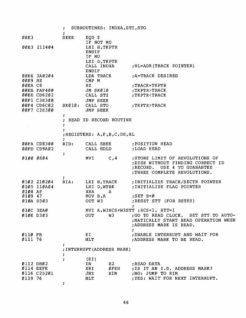
0QJE3
0QJE3 211404
0QJE6 3AQJ2QJ4 00E9 BE 0QJEA C8 QJQJEB FAF4QJ0 0QJEE CD62QJ2 0QJF1 C3E3QJQJ 0QJF4 CD6C02 00F7 C3E300
0QJFA CDE300 00FD CD9A02
0100 0E04
0102 210204 0105 110A04 0108 AF 0109 47 010A D303
010C 3EA0 010E D303
0110 FB 0111 76
0112 DB02 0114 EEFE 0116 C25201 0119 76
SUBROUTINES: INDXA,STI,STO . , SEEK EQU $
IF NOT MU LXI H,TKPTR ENDIF IF MU LXI D,TKPTR CALL INDXA ENDIF LDA TRACK CMP M RZ JM SK010 CALL STI JMP SEEK
SK010: CALL STO JMP SEEK
i i READ ID RECORD ROUTINE
i
iHL=ADR(TRACK POINTER)
iA=TRACK DESIRED
iTRACK=TKPTR iTKPTR)TRACK iTKPTR<TRACK
iTKPTR)TRACK
iREGISTERS: A,F,B,C,DE,HL
RID:
. , RIA:
i
CALL SEEK CALL HDLD
MVI C,4
LXI H,TRACK LXI D,WTRK XRA A MOV B,A OUT W3
iPOSITION HEAD iLOAD HEAD
iSTORE LIMIT OF REVOLUTIONS OF iDISK WITHOUT FINDING CORRECT ID iRECORD. USE 4 TO GUARANTEE iTHREE COMPLETE REVOLUTIONS .
iINITIALIZE TRACK/SECTR POINTER iINITIALIZE FLAG POINTER
iSET 8=0 iRESET STT (FOR RETRY) i
MVI A,W3RCS+W3STT iRCS=l, STT=l OUT W3 iGO TO READ CLOCK. SET STT TO AUTO
iMATICALLY START READ OPERATION WHEN iADDRESS MARK IS RE!\D.
EI HLT
i iENABLE INTERRUPT AND WAIT FOR iADDRESS MARK TO BE READ.
iINTERRUPT(ADDRESS MARK)
(EI) IN XRI JNZ HLT
R2 0FEH RIM
46
iREAD DATA iIS IT AN I.D. ADDRESS MARK? iNO: JUMP TO RIM iYES: WAIT FOR NEXT INTERRUPT.

011A OB02 011C AE 0110 12 011E 13 011F 76
0120 OB02 0122 12 0123 13 0124 23
0125 76
0126 OB02 0128 AE 0129 47 012A 3E21 012C 0303
012E 76
012F OB02
0131 12 0132 13
0133 76
iINTERRUPT(TRACK ADDRESS)
(EI) IN R2 XRA M STAX D INX D HLT
iREAD TRACK ADDRESS BYTE. iCOMPARE WITH DESIRED TRACK iWTRK =0 FOR OK, =NON-ZERO FOR ERROR iDE POINTS TO ZER01 iWAIT FOR NEXT INTERRUPT
iINTERRUPT(FIRST ZERO BYTE)
i (EI) IN R2 STAX D INX D INX H
HLT i
iREAO ZERO BYTE iZER01 =0 FOR OK, =NON-ZERO FOR ERROR iDE POINTS TO ZER02 iHL POINTS TO SECTR . , iWAIT FOR NEXT INTERRUPT
iINTERRUPT(SECTOR ADORESS)
i
(EI) IN XRA MOV MVI OUT
HLT
R2 iREAD SECTOR ADDRESS BYTE M iCOMPARE WITH DESIRED SECTOR B,A iB =0 FOR OK, =NON-ZERO FOR ERROR A,W3STT+W3CCW W3 iSEND COMMAND TO W3.
iTHIS COMMAND SETS CCW. (STT iBIT MUST ALSO BE A ONE TO AVOID iRESETTING STT.) THE BIT RING PULSE i (BRP) FOLLOWING THE SETTING OF CCW iWILL START A BIT BY BIT COMPARISON iOF THE DATA READ FROM THE DISK WITH iTHE DATA READ FROM THE CRC REGISTER. i (ALTHOUGH THE CPU WILL READ THE iCOMPLETED 2ND ZERO BYTE AT THE NEXT iBRP, THE DISK DRIVE HEAD WILL BEGIN iREADING THE 1ST CRC BYTE.)
iWAIT FOR NEXT INTERRUPT.
iINTERRUPT(SECOND ZERO BYTE)
i
(EI) IN
STAX D INX D
HLT
R2
iINTERRUPT(CRC BYTE 1)
(EI)
iREAD 2ND ZERO BYTE i iZER02 =0 FOR OK, =NON-ZERO FOR ERROR iDE POINTS TO CRCID ; iWAIT FOR NEXT INTERRUPT.
47
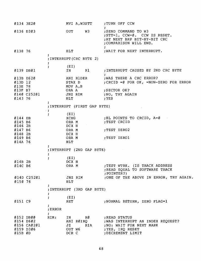
0134 3E20
0136 D303
0138 76
0139 DB01
013B E620 013D 12 013E 78 013F B7 0140 C25201 0143 76
0144 EB 0145 B6 0146 2B 0147 B6 0148 2B 0149 B6 014A 76
014B 2B 014C B6
014D C25201 0150 76
0151 C9
0152 DB00 0154 E602 0156 CA0201 0159 D306 015B 0D
. I
MVI A,W3STT
OUT W3
HLT
;INTERRUPT(CRC BYTE 2)
i
(EI) IN R1
ANI RIDER STAX D MOV A,B ORA A JNZ RIM HLT
;TURN OFF CCW i iSEND COMMAND TO W3 iSTT=l, CCW=0. CCW IS RESET. iAT NEXT BRP BIT-BY-BIT CRC iCOMPARISON WILL END. i iWAIT FOR NEXT INTERRUPT.
iINTERRUPT CAUSED BY 2ND CRC BYTE . , iWAS THERE A CRC ERROR? iCRCID =0 FOR OK, =NON-ZERO FOR ERROR
iSECTOR OK? iNO, TRY AGAIN iYES
iINTERRUPT (FIRST GAP BYTE)
i
(EI) XCHG ORA M DCX H ORA M DCX H ORA M HLT
iHL POINTS TO CRCID, A=0 iTEST CRCID
iTEST ZER02
iTEST ZER01
iINTERRUPT (2ND GAP BYTE)
. ,
(EI) DCX H ORA M
JNZ RIM HLT
iTEST WTRK. (IS TRACK ADDRESS iREAD EQUAL TO SOFTWARE TRACK i POINTER?) iONE OF THE ABOVE IN ERROR, TRY AGAIN.
iINTERRUPT (3RD GAP BYTE)
i i ERROR
RIM:
(EI) RET
IN R0 ANI R0IRQ JZ RIA OUT W6 DCR C
48
iNORMAL RETURN, ZERO FLAG=1
iREAD STATUS iWAS INTERRUPT AN INDEX REQUEST? iNO: WAIT FOR NEXT MARK i YES, IRQ RESET iDECREMENT LIMIT

015C C20201
015F AF 0160 D303
0162 3E01 0164 320904 0167 B7 0168 C9
0169 CDFA00 016C C0 016D 3E60 016F D303 0171 0609 0173 76
0174 05 0175 C27301 0178 76
0179 3E40 017B D303
017D 218004
0180 1621
0182 0EFB
0184 3A0404 0187 D603
JNZ
XRA A OUT
MVI A,l STA NOGO ORA A RET
RIA
W3
iWAIT FOR NEXT MARK IF NOT 3RD COMPLETE iREVOLUTION OF DISK WITHOUT SUCCESS i iQUIT iRESET STT
iCOULD NOT FIND REQUESTED ID iCLEAR ZERO FLAG i ERROR RETURN
READ DATA RECORD i iREGISTERS: A,F,B,C,DE,HL
CALL READ ID RECORD FIRST i READ:
RGAP: i
CALL RID iREAD ID RNZ iERROR IN RID, RETURN MVI A,W3WCS+W3STT OUT W3 iSET WRITE CLOCK, LEAVE STT SET MVI B,9 iPASS GAP BYTES 4-12 HLT
iINTERRUPT (GAP BYTE 4-12)
(EI) DCR JNZ HLT
B RGAP
iINTERRUPT (GAP BYTE 13)
(EI) MVI A,W3WCS OUT W3
LXI H,BUFFR
iWAIT FOR GAP BYTE 13. HEAD HAS iNOW PASSED AREA IN GAP THAT CONTAINS iUNKNOWN INFORMATION GENERATED WHEN iWRITE CURRENT WAS TURNED ON TO WRITE iDATA RECORD.
iRESET STT, SET WRITE CLOCK TO iPREVENT INTERRUPTS UNTIL FOLLOWING iIS DONE. i iSET HL TO 1ST ADDRESS OF iSTORAGE BUFFER . . ,
MVI D,W3STT+W3CCW iSTORE COMMAND TO SET CCW IN iD REGISTER. i
MVI C,0FBH iSTORE DATA ADDRESS MARK CODE iIN C.
LDA SCTSZ SUI 3
i iSET SECTOR SIZE
49

0189 47
018A 3EA0 018C D303 018E 76
018F DB02 0191 B9 0192 C2C501 0195 76
0196 DB02 0198 77
0199 23 9A 76
019B DB02 019D 77 019E 05 019F C29901 01A2 23 01A3 76
01A4 DB02 01A6 77
01A7 7A 01A8 D303 01AA 76
01AB 23 01AC DB02 01AE 77 01AF 76
MOV B,A iSAVE COUNT IN B i
MVI A,W3RCS+W3STT iSET READ CLOCK, SET STT. OUT W3 HLT iWAIT FOR ADDRESS MARK.
iINTERRUPT (ADDRESS MARK)
i
(EI) IN R2 CMP C JNZ HLT
MARK
iINTERRUPT (DATA BYTE 1)
(EI) IN R2 MOV
RLOOP: INX
. , HLT
M,A
H
iREAD BYTE iIS IT A DATA ADDRESS MARK? iNa: JUMP TO MARK iWAIT FOR FIRST DATA BYTE
iYES: READ FIRST DATA BYTE iSTORE FIRST DATA BYTE i iREAD AND STORE DATA BYTES
iINTERRUPT (DATA BYTES 2-(SCTSZ-2) )
. ,
(EI) IN R2 MOV DCR JNZ INX HLT
M,A B RLOOP H
iINTERRUPT (DATA BYTE #(SCTSZ-1) )
i
(EI) IN R2 MOV M,A
MOV A,D OUT W3 HLT
iREAD AND STORE DATA BYTE
iSET CCW
iINTERRUPT (DATA BYTE #SCTSZ)
i
(EI) INX H IN R2 MOV M,A HLT
;READ AND STORE LAST DATA BYTE
:INTERRUPT (FIRST CRC BYTE)
(EI)
50

01B0 3E20 01B2 D303 01B4 76
01B5 DB01 01B7 47 01B8 AF 01B9 D303
01BB 78
01BC E620 01BE 320E04 01Cl C8
01C2 C3DA01
01C5 AF 01C6 D303 01C8 DB02 01CA DEF8 01CC 320F04 01CF C2D601 01D2 3C 01D3 C3D701 01D6 AF 0107 321004 01DA 211204 01DD 35 01DE C26901 01El AF 01E2 D303 01E4 3C
01E5 C9
01E6 CDFA00 01E9 C0
01EA 0606 01EC 76
;
MVI A,W3STT OUT W3 HLT
;RESET CCW
;INTERRUPT (2ND CRC BYTE)
MARK:
MK010: MK020: MK030:
(EI) IN Rl MOV B,A XRA A OUT W3
MOV A,B
ANI RIDER STA CRCDR RZ
JMP MK030
XRA A OUT W3 IN R2 SBI 0F8H STA ILLMK JNZ MK010 INR A JMP MK020 XRA A STA DELMK LXI H,RRTRY DCR M JNZ READ XRA A OUT W3 INR A
RET
;READ STATUS ;SAVE STATUS
;RESET STT. (372 GOES TO WRITE ;CLOCK AUTOMATICALLY.) . , ;RECALL STATUS
;IS THERE A CRC ERROR? ;SET CRC DATA RECORD FLAG iNO, NORMAL RETURN
; ;READ RECORD BUT FOUND ;CRC ERROR ; ;RESET STT
;READ MARK AGAIN ;IS IT A "DELETED DATA MARK"? ;SET ILLEGAL MARK FLAG ;ILLEGAL MARK ;DELETED DATA MARK
;ILLEGAL MARK ;SET DELETED DATA MARK FLAG ;CHECK FOR RETRY
;TRY AGAIN
;RESET STT ;CLEAR ZERO FLAG TO ;INDICATE AN ERROR CONDITION
WRITE DATA RECORD ROUTINE ; ;REGISTERS: A,F,B,C,DE,HL
CALL READ ID RECORD ROUTINE FIRST
WRITE: CALL RID RNZ
MVI B,6 WGAP: HLT
;READ ID ;ERROR IN RID, RETURN ; ;COUNT 6 MORE INTERRUPTS FROM ID ;RECORD. (HEAD WILL THEN BE
51

01EO 05 01EE C2EC01
01F1 3EB8 01F3 D301
01F5 AF 01F6 D302 01F8 76
01F9 3E70 01FB D303
01FO DB01 01FF E604 0201 CA1602 0204 3E02 0206 CDC802 0209 3E02 020B CDC002 020E 3E01 0210 321104 0213 C3C600
0216 76
0217 76
0218 76
0219 76
iINTERRUPT
(EI) OCR B iREADING 10TH BYTE) JNZ WGAP
i MVI A,W1CBS+W1CBN jSET CLOCK BITS AND STROBE OUT WI jSET WRITE CLOCK LOGIC TO WRITE
iALL CLOCK BITS ("FF" CLOCK BITS) jFOR DATA
XRA A OUT W2 HLT
iINTERRUPT
(EI)
i jSET WRITE DATA REGISTER TO 00.
jWAIT FOR INTERRUPT
i (10TH INTERRUPT SINCE ID RECORD. jHEAD IS READING GAP BYTE 11.) i
MVI OUT
A,W3WCS+W3STT+W3WES iWCS, STT, WES = 1 W3 iWRITE CURRENT AND WRITE CLOCK
IN R1 ANI R1WFT JZ WR010 MVI A, ~v0WFR CALL SETW0 MVI A,W0WFR CALL CLRW0 MVI A,l STA WRITF JMP ERROR
WR010: HLT j
iINTERRUPT
. ,
(EI) HLT
iINTERRUPT
(EI) HLT
i iINTERRUPT
(EI) HLT
52
iWILL START AT NEXT BRP iREAD STATUS iWRITE FAULT? iNO, CONTINUE
jWRITE FAULT RESET
iCLEAR RESET BIT
iYES, SET WRITE FAULT FLAG
i iWAIT FOR INTERRUPT
iHEAD BEGINS WRITING. WRITES 00 iIN GAP BYTE 12 (11TH INTERRUPT jSINCE ID RECORD)
i12TH INTERRUPT. HEAD WRITES 00 iIN BYTE 13
i13TH INTERRUPT. HEAD STARTS BYTE 1

021A 218004 021D 76
021E 06FB
0220 0E22
0222 16B8
0224 lE20
0226 3E80
0228 76
0229 D301
022B 78 022C D302
022E 79 022F D303
0231 7A
0232 76
0233 D301
0235 7B 0236 D303
0238 7E
iINTERRUPT
(EI) LXI H,BUFFR HLT
i iINTERRUPT
iSET H,L TO START OF WRITE BUFFER i (14TH INTERRUPT. HEAD STARTS BYTE 15)
(EI) MVI B,0FBH iLOAD DATA MARK IN B
i (15TH INTERRUPT. HEAD STARTS BYTE 16) ,
MVI C,W3STT+W3CCG iSTORE SET CCG COMMAND IN C ;
MVI D,WICBS+WICBN iSTORE "FF" CLOCK PATTERN iCOMMAND IN D i
MVI E,W3STT iSTORE RESET CCG COMMAND IN E i
MVI A,WICBS+WICBD iSTORE "C7" DATA MARK CLOCK
HLT i iINTERRUPT
(EI) OUT WI
MOV A,B OUT W2
~10V A,C OUT W3
MOV A,D
HLT
iINTERRUPT
(EI) OUT WI
r.-l0V A,E OUT W3
MOV A,M
iPATTERN COMMAND IN A i iWAIT FOR INTERRUPT
iSET "C7" DATA MARK CLOCK PATTERN. i (16TH INTERRUPT. HEAD WRITING i17TH AND LAST GAP BYTE) i iSET "FB" DATA BITS FOR ;DATA MARK i iSET CCG. THIS CAUSES CRC iCALCULATION TO BEGIN AT NEXT BRP. i iGET "FF" DATA BIT CLOCK iPATTERN IN A i iWAIT FOR INTERRUPT.
iSET "FF" DATA BIT CLOCK PATTERN iFOR NEXT BYTE. HEAD NOW BEGINS iWRITING DATA MARK i iRESET CCG. (CCG MUST BE RESET iBEFORE NEXT BRP OR CRC CALCULATION iWOULD BEGIN AGAIN.) i iLOAD FIRST DATA BYTE IN
53

0239 D302.
023B 76
023C 3A0404 023F 3D 0240 47
0241 23 0242 7E 0243 D302 0245 76
·0246 05 0247 C24102
024A 3E21 024C D303
024E 76
024F 76
0250 3EFF 0252 D302
0254 3E20 0256 D303
0258 76
0259 3E24 025B D303
. ,
OUT W2
HLT
iINTERRUPT
(EI) LDA SCTSZ DCR A MOV B,A
hLOOP: INX H
. ,
MOV A,M OUT W2 HLT
iINTERRUPT
(EI) DCR B JNZ WLOOP
i iWAIT FOR INTERRUPT
iSET SECTOR SIZE
iSAVE COUNT IN B. HEAD iBEGINS WRITING FIRST DATA BYTE. i iWRITE DATA BYTES 2 THRU NBSCT
i MVI A,W3STT+W3CCW iSET CCW. IN WRITE MODE THE 372 OUT W3 iWILL BEGIN WRITING BITS FROM THE
iCRC REGISTER AT THE NEXT BRP iFOLLOWING THE SETTING OF CCW. i (HEAD IS WRITING DATA BYTE 128) i
HLT iWAIT FOR INTERRUPT i iINTERRUPT
i
(EI) HLT
i INTERRUPT
(EI) MVI A,0FFH OUT W2
MVI A,W3STT OUT W3
HLT i iINTERRUPT
(EI)
iHEAD STARTS WRITING FIRST CRC BYTE
iLOAD FF GAP BYTE IN WRITE DATA iREGISTER (HEAD BEGINS WRITING i 2ND CRC BYTE.) . , iRESET CCW COMMAND. CRC BIT iWRITING WILL STOP AT NEXT BRP. i iWAIT FOR INTERRUPT.
MVI A,W3STT+W3WER iWRITE ENABLE RESET. WRITE OUT W3 iCURRENT WILL STOP AT NEXT
iBRP. (HEAD BEGINS WRITING 1ST
54

025D 76
025E AF 025F D303
0261 C9
0262 CDD002 0265 06C0 0267 3E01 0269 C37302
026C CDD002 026F 0680 0271 3EFF
0273
0273 211404
0276 86 0277 77 0278 3E2B 027A BE 027B 3E04 027D FA8602 0280 CDC002
0283 C38902 0286 CDC802
0289 78 028A D304 028C F620 028E D304 0290 E6DF 0292 D304
i GAP BYTE.) i
HLT iWAIT FOR INTERRUPT i i INTERRUPT
(EI) XRA A iRESET STT. OUT W3
i RET iDATA RECORD IS WRITTEN.
STEP IN REGISTERS: A,F,B,DE,HL
; SUBROUTINES: INDXA,UNSLC,DELAY,SETW0 STI: CALL UNSLC
MVI B,W4STS+W4SID MVI A,l ;INCREMENT TKPTR JMP ST010
STEP OUT REGISTERS: A,F,B,DE,HL . SUBROUTINES: INDXA,UNSLC,DELAY,CLRW0 ,
STO: CALL UNSLC MVI B,W4STS r-1VI A,-l iDECREMENT TKPTR . ,
ST010 EQU $ IF NOT MU LXI H,TKPTR ENDIF IF MU LXI D,TKPTR CALL INDXA ENDIF ADD M iINC/DEC TKPTR f\10V M,A MVI A,LHCTK ;CHECK FOR WRITE CURRENT CHANGE CMP M ;A=LHCTK-TKPTR MVI A,W0LCT JM ST020 ;TRACK)LHCTK CALL CLRW0 ;TRACK<OR=LHCTK,
;TURN OFF LOW CURRENT JMP ST030
ST020: CALL SETW0 iTRACK)LHCTK, iTURN ON LOW CURRENT
ST030: MOV A,B OUT W4 ;SET DIRECTION ORI W4S0S iTURN ON SOS OUT W4 ;RISING EDGE OF SOS ANI NOT W4S0S iTURN OFF SOS OUT W4 iTRAILING EDGE OF SOS
55

0294 060A 0296 CDE202 0299 C9
029A
029A 211604
029D 7E 029E B7 029F C0 02A0 CDD002 02A3 3E08 02A5 CDC802 o 2A8 0628 02AA CDE202 02AD 3E01 02AF C3BB02
02B2 CDD002 02B5 3E08 02B7 CDC002 02BA AF 02BB
02BB 211604
02BE 77 02BF C9
02C0 211304 02C3 2F 02C4 A6 02C5 C3CC02 02C8 211304
DELAY 10 MSEC MVI B,10 CALL DELAY RET
HEAD LOAD SUBROUTINE REGISTERS: A,F,B,DE,HL SUBROUTINES: UNSLC,DELAY,INDXA,SETW0
HDLD EQU $ IF NOT MU LXI H,HEAD ENDIF IF MU LXI D,HEAD CALL INDXA ENDIF MOV A,M ORA A RNZ CALL UNSLC MVI A,W0HLD CALL SETW0 MVI B,40 CALL-DELAY MVI A,l JMP UL010
iCHECK HEAD STATUS
iIS HEAD LOADED ALREADY? iYES iNO, SELECT UNIT
iLOAD HEAD iWAIT 40 MSEC
iSET HEAD STATUS
UNLOAD HEAD SUBROUTINE REGISTERS: A,F,DE,HL SUBROUTINES: UNSLC,INDXA,CLRW0
UNLD: CALL UNSLC MVI A,W0HLD CALL CLRW0 iUNLOAD HEAD XRA A
UL010 EQU $ iUPDATE HEAD STATUS
i
IF NOT MU LXI H,HEAD ENDIF IF MU LXI D,HEAD CALL INDXA ENDIF MOV M,A RET
iWR0 MANAGER A=BITS TO BE CLEARED/SET
i REGISTERS: A,F,HL CLRW0: LXI H,WR0
CMA ANA M iCLEAR JMP CR010
SETW0: LXI H,WR0
56

02CB B6 02CC 0300 02CE 77 02CF C9
0200
0200 3E01
0202 F604 02D4 D304 02D6 DB00 02D8 E640 02DA C0 02DB 2F 02DC 320804 02DF C3C600
02E2 3E04 02E4 D306
02E6 DB00 02E8 E604 02EA CAE602 02ED 05 02EE C2E202 02Fl C9
ORA M iSET CR010: OUT W0
MOV M,A iSAVE A COpy OF W0 RET
UNIT SELECT SUBROUTINE UNIT=UNIT#(1-4)
REGISTERS: A,F i ERROR RETURN: JMP ERROR UNSLC EQU $
IF NOT MU MVI A,l ENOIF IF MU LOA UNIT OCR A iA=0-3 ANI W4UBA iMASK UNIT# ENOIF ORI W4UBS iTURN ON STROBE OUT W4 iSELECT UNIT IN R0 iCHECK FOR READY ANI R0RYB iREADY? RNZ iYES CMA iNO STA SLCTF iSET FLAG JMP ERROR
i DELAY SUBROUTINE B= # OF MSEC (MAX=256 WITH B=0)
REGISTERS: A,F,B i DELAY: MVI A,W6TRR
OUT W6 iTURN ON TRR iRESET TIMER REQUEST
i WAIT FOR TRQ RST D010: IN R0
STATUS
ANI R0TRQ JZ D010 DCR B JNZ DELAY RET
IF MU
iREAD STATUS iCHECK FOR TRQ iWAIT FOR 1 MSEC iDONE? iNO iYES
iINDEXED ADDRESSING SUBROUTINE INPUT:DE=BASE
i UNIT=INDEX i OUTPUT:HL=DE+(UNIT-l) i REGISTERS: F,DE,HL INDXA: LXI H,UNIT
57

02F2 CDIF00
02F5 CD9A02 eJ2F8 210100
02FB 3EB8 02FD D301 02FF 3EFF 0301 D302 0303 AF 0304 D303 0306 3E78 0308 D303
030A FB 030B 76
030C 3E02 030E D306
0310 0627 0312 76
0313 05 0314 C21203 0317 AF 0318 D302 031A 0605 031C 76
031D 05 031E C21C03
i
MOV L,M MVI H,0 DCR L DAD D RET ENDIF
DISK FORMATTING ROUTINE
FRMAT: CALL INIT iINITIALIZE DISK UNIT
i
INITIALIZE ADDRESS POINTERS CALL HDLD iLOAD HEAD LXI H,1 iH=00=TRACK ADDRESS
iL=01=SECTOR ADDRESS
SET UP COMMANDS FM030: MVI A,WICBS+WICBN
OUT WI iSET CLOCK BITS MVI A,0FFH OUT W2 iSET WRITE DATA=0FFH XRA A OUT W3 iRESET STT MVI A,W3WCS+W3STT+W3WES+W3IXS OUT W3 iSET 372 TO START WRITING
iAT INDEX HOLE EI iENABLE INTERRUPTS AND HLT iWAIT FOR INDEX
INTERRUPT ( INDEX START)
(E I) HEAD IS WRITING FIRST GAP BYTE MVI A,W6IRR OUT W6 iRESET INDEX REQUEST
i WRITE PRE-INDEX GAP MVI B,39 i B=NUMBER OF OFFH GAP BYTES
FM040: HLT iWAIT FOR BRP INTERRUPT
INTERRUPT (DATA REQUEST)
FM050:
(EI) DCR B JNZ FM040 XRA A OUT W2 MVI B,5 HLT
HEAD WRITES GAP BYTES 2-40 iDONE? i NO, REPEAT iYES, CHANGE GAP iBYTE TO 00H iB=BYTE COUNT
INTERRUPT
(EI) HEAD WRITES GAP BYTES 41-45 DCR B iDONE? JNZ FM050 i NO, REPEAT
58

0321 76
0322 3E90 0324 D301 0326 3EFC 0328 D302 032A 76
032B 3EB8 032D D301 032F 3EFF 0331 D302 0333 061A 0335 76
0336 05 0337 C23503
033A AF
033B D302 033D 76
033E 76
033F 76
0340 76
0341 76
HLT iYES
INTERRUPT
(EI) HEAD IS WRITING GAP BYTE 46 WRITE INDEX ADDRESS MARK
MVI A,WICBS+WICBI OUT WI iCHANGE CLOCK BITS MVI A,0FCH OUT W2 iSET WRITE DATA=0FCH HLT iWRITE MARK
INTERRUPT
(EI) HEAD IS WRITING INDEX ADDRESS MARK WRITE POST-INDEX GAP
MVI A,WICBS+WICBN OUT WI iSET CLOCK BITS MVI A,0FFH OUT W2 iSET WRITE DATA=0FFH MVI B,26 i B=BYTE COUNT
FM060: HLT iWRITE GAP BYTE
i
INTERRUPT
(EI) DCR B JNZ FM060
FM070: XRA A
OUT V12 HLT
INTERRUPT
(EI) HLT
INTERRUPT
(EI) HLT
INTERRUPT
(EI) HLT
INTERRUPT
(EI) HLT
HEAD WRITES GAP BYTES 1-26 iDONE? i NO, REPEAT
iBEGINNING OF SECTOR WRITE LOOP i-EXECUTED 26 TIMES iSET WRITE DATA=00H
HEAD IS WRITING 1ST OF 6 00 BYTES
2ND OF 6
3RD OF 6
4TH OF 6
59

0342 06FE 0344 0E22
0346 16B8
0348 lE20 034A 3E80
034C 76
034D D301 034F 78 0350 D302 0352 79 0353 D303 0355 7A
0356 76
0357 D301
0359 7B 035A D303
035C 7C 035D D302 035F 76
0360 AF 0361 D302 0363 76
0364 7D 0365 D302 0367 76
INTERRUPT
(EI) 5TH OF 6 MVI B,0FEH ; LOAD ID MARK IN B MVI C,W3STT+W3CCG ; STORE SET CCG COMMAND IN C
; (ALSO RESETS IXS) MVI D,WICBS+WICBN ; STORE "FF" CLOCK PATTERN
;COMMAND IN D MVI E,W3STT ; STORE RESET CCG COMMAND IN E MVI A,WICBS+WICBD ; STORE "C7" DATA MARK CLOCK
;PATTERN COMMAND IN A HLT
INTERRUPT
(EI) OUT WI MOV A,B OUT W2 MOV A,C OUT W3 MOV A,D
HLT
INTERRUPT
(EI) OUT WI
MOV A,E OUT W3
MOV A,H OUT W2 HLT
INTERRUPT
(EI) XRA A OUT W2 HLT
INTERRUPT
(EI) MOV A,L OUT W2 HLT
INTERRUPT
HEAD IS WRITING 6TH OF 6 00 GAP BYTES ;SET "C7" DATA MARK CLOCK PATTERN. ;SET "FE" DATA BITS FOR ; ID MARK ;SET CCG. THIS CAUSES CRC ;CALCULATION TO BEGIN AT NEXT BRP. ;GET "FF" DATA CLOCK BIT ;PATTERN IN A
HEAD IS WRITING ID ADDRESS MARK ;SET "FF" DATA CLOCK BIT PATTERN ;FOR NEXT BYTE. HEAD NOW BEGINS ;WRITING ID MARK ;RESET CCG. (CCG MUST BE RESET ;BEFORE NEXT BRP OR CRC CALCULATION ;WOULD BEGIN AGAIN.) ;LOAD TRACK ADDRESS
;WAIT FOR INTERRUPT
HEAD IS WRITING TRACK ADDRESS
;SET DATA BYTE=00W
HEAD IS WRITING FIRST ZERO BYTE
;SET DATA BYTE=SECTOR ADDRESS
60

0368 AF 0369 D302 036B 76
0'36C 3E21 036E D303
0370 76
0371 76
0372 3EFF 0374 D302 0376 3E20 0378 D303 037A 060B 037C 76
037D 05 037E C27C03 0381 AF 0382 D302 0384 76
0385 76
0386 76
0387 76
0388 76
0389 06FB 038B 0E22 038D 16B8
038F lE20
(EI) XRA A OUT W2 HLT
HEAD IS WRITING SECTOR ADDRESS
iSET DATA BYTE=00H
INTERRUPT
(EI) HEAD IS WRITING 2ND ZERO BYTE MVI A,W3STT+W3CCW i SET CCW. IN WRITE MODE THE 372 OUT W3 iWILL BEGIN WRITING BITS FROM THE
iCRC REGISTERS AT THE NEXT BRP iFOLLOWING THE SETTING OF CCW.
HLT iWAIT FOR INTERRUPT
INTERRUPT
(EI) HLT
HEAD IS WRITING FIRST CRC BYTE
INTER~UPT
FM080:
(EI) HEAD MVI A,0FFH OUT W2 MVI A,W3STT OUT W3 MVI B,ll HLT
IS WRITING 2ND CRC BYTE i LOAD FF GAP BYTE IN WRITE DATA iREGISTER i RESET CCW COMMAND. CRC BIT iWRITING WILL STOP AT NEXT BRP. i B=BYTE COUNT
INTERRUPT
(EI) HEAD WRITES GAP BYTES 1-11 DCR B iDONE? JNZ FM080 i NO, REPEAT XRA A iYES, CHANGE GAP BYTE OUT W2 iTO 00H HLT (EI) BYTE 12 HLT (EI) BYTE 13 HLT (EI) BYTE 14 HLT (EI) BYTE 15
HLT
INTERRUPT
(EI) HEAD IS WRITING GAP BYTE 16 MVI B,0FBH i LOAD DATA MARK IN B MVI C,W3STT+W3CCG i STORE SET CCG COMMAND IN C MVI D,WICBS+WICBN i STORE "FF" CLOCK PATTERN
iCOMMAND IN D MVI E,W3STT i STORE RESET CCG COMMAND IN E
61

0391 3E80
0393 76
039,4 D301 0396 78 0397 D302 0399 79 039A D303 039C 7A
039D 76
039E D301
03A0 7B 03A1 D303
03A3 3EE5 03A5 D302 03A7 76
03A8 067F 03AA 76
03AB 05 03AC C2AA03
03AF 3E21 03B1 D303
03B3 76
03B4 76
MVI A,W1CBS+W1CBD i STORE "C7" DATA MARK CLOCK iPATTERN COMMAND IN A
HLT iWAIT FOR INTERRUPT
INTERRUPT
(EI) OUT WI MOV A,B OUT W2 MOV A,C OUT W3 MOV A,D
HLT
INTERRUPT
HEAD IS WRITING GAP BYTE 17 iSET "C7" DATA MARK CLOCK PATTERN. iSET "FB" DATA BITS FOR iDATA MARK iSET CCG. THIS CAUSES CRC iCALCULATION TO BEGIN AT NEXT BRP. iGET "FF" DATA BIT CLOCK iPATTERN IN A iWAIT FOR INTERRUPT.
(EI) HEAD IS WRITING DATA ADDRESS MARK OUT WI
MOV A,E OUT W3
MVI A,0E5H OUT W2 HLT
INTERRUPT
iSET "FF" DATA BIT CLOCK PATTERN i FOR NEXT BYTE. iRESET CCG. (CCG MUST BE RESET iBEFORE NEXT BRP OR CRC CALCULATION iWOULD BEGIN AGAIN.) iLOAD DATA
(EI) DATA BYTE 1 MVI B,NBSCT-1
FMI00: HLT
INTERRUPT
(EI) HEAD WRITES DATA BYTES 2-NBSCT DCR B JNZ FM100
MVI A,W3STT+W3CCW i SET CCW. IN WRITE MODE THE 372 OUT W3 iWILL BEGIN WRITING BITS FROM THE
iCRC REGISTERS AT THE NEXT BRP iFOLLOWING THE NEXT SETTING OF CCW.
HLT
INTERRUPT
, (EI) HLT
INTERRUPT
HEAD IS WRITING FIRST CRC BYTE
(EI) HEAD IS WRITING 2ND CRC BYTE
62

03B5 3EFF 03B7 D302 03B9 3E20 03BB D303 03BD 061B 03BF 76
03C0 05 03C1 C2BF03
03C4 2C 03C5 3E1A 03C7 BD 03C8 F23A03
03CB 76
03CC DB00 03CE E602 03D0 CACB03
03D3 3E04 03D5 D303
03D7 3E4C 03D9 BC 03DA C8 03DB 2E01 03DD 24 03DE E5 03DF 0602 03E1 CDE202 03E4 CD6202 03E7 E1 03E8 C3FB02
03EB
0400
0401 0402 0403
MVI A,0FFH OUT W2 MVI A,W3STT OUT W3 MVI B,27
FMl10: HLT
i INTERRUPT
i (EI) HEAD OCR B JNZ FMl10
INR L MVI A,26 CMP L JP FM070
i LOAD FF GAP BYTE IN WRITE DATA iREGISTER
RESET CCW COMMAND. CRC BIT WRITING i ENDS i B=BYTE COUNT
vlRITES GAP BYTES 1-27 iDONE? i NO, REPEAT
iINCREMENT SECTOR ADDRESS
iLAST SECTOR? i NO, WRITE ANOTHER SECTOR
i WRITE FF'S TO END OF TRACK FM120: HLT
INTERRUPT
(EI) IN R0
HEAD WRITES GAP BYTES 28 TO 247 iREAD STATUS
ANI R0IRQ JZ FM120
END OF TRACK MVI A,W3WER OUT W3
MVI A,NTRKS-1 CMP H RZ MVI L,l INR H PUSH H MVI B,02 CALL DELAY CALL STI POP H JMP FM030
ORG 0400H iCOMMAND CMND: OS 1 i i PARAMETERS UNIT: OS 1 TRACK: OS 1 SECTR: DS 1
i INDEX REQUEST? i NO, CONTINUE
iWRITE ENABLE AND STT RESET. iINDEX REQUEST IS AUTOMATICALLY RESET iBY STT RESET.
iLAST TRACK? i YES, FORMATTING COMPLETE i NO, RESET SECTOR ADDRESS iINCREMENT TRACK ADDRESS iSAVE HL iWAIT FOR TUNNEL ERASE HEAD iTO REACH END OF TRACK BEFORE iSTEPPING HEAD. iRESTORE HL i CONTINUE
iCOMMAND(l-NCMDS)
iFDD UNIT BEING COMMANDED iTRACK DESIRED iSECTOR DESIRED
63

0404 0004
0405 0406 0407 0408 0409 040A 040B 040C 040D 040E 040F 0410 0411 000D
0412 0413 0414 0415 0416 0017
0417
0480
SCTSZ: NP i i FLAGS MERF: CMDER: PRMER: SLCTF: NOGO: WTRK: ZER01 : ZER02 ~ CRCID: CRCDR: ILLMK: DELMK: WRITF: NF i
DS 1 EQU $-UNIT
DS 1 DS 1 DS 1 DS 1 DS 1 DS 1 DS 1 DS 1 DS 1 DS 1 DS 1 DS 1 DS 1 EQU $-MERF
iCOUNTERS, POINTERS, RRTRY: DS 1 WR0: DS NU TKPTR: DS NU REVS: DS NU HEAD: DS NU NB EQU $-CMND
iSTACK
ORG 480H
i DATA BUFFER BUFFR: DS NBSCT
END
64
iSECTOR SIZE iNO. OF PARAMETERS
iMASTER ERROR FLAG iCOMMAND ERROR FLAG iPARAMETER ERROR FLAG iSELECT FAULT iFAILED TO FIND SECTOR FLAG iWRONG TRACK FLAG iZERO BYTE 1 NOT ZERO FLAG iZERO BYTE 2 NOT ZERO FLAG iCRC ERROR IN ID FLAG iCRC ERROR IN DATA READ FLAG iILLEGAL DATA MARK FLAG iDELETED DATA MARK FLAG iWRITE FAULT FLAG iNUMBER OF FLAGS
STATUSES iREAD RETRY COUNTER iCOPIES OF LATEST W0 iTRACK POINTER FOR EACH UNIT iELAPSED IDLE REVOLUTIONS iHEAD STATUS (l=LOADED, 0=UNLOADED) iNO. OF BYTES IN DATA AREA
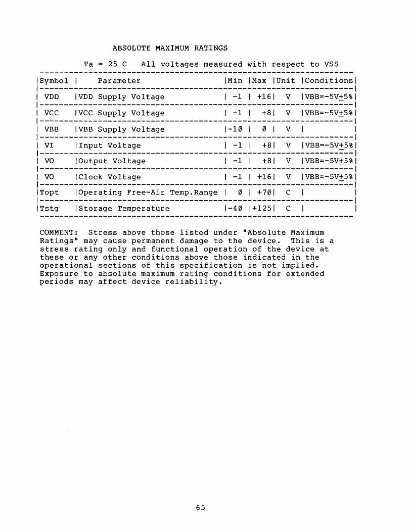
ABSOLUTE MAXIMUM RATINGS
Ta = 25 e All voltages measured with respect to VSS
Symbol 1 Parameter IMin IMax IUnit IConditions
VDD IVDD Supply Voltage 1 -1 1 +161 V IVBB=-5V±5%
vec Ivee Supply Voltage 1 -1 1 +81 V IVBB=-5V±5%
VBB IVBB Supply Voltage 1-10 1 0 1 V
VI 1 Input Voltage 1 -1 1 +81 V IVBB=-5V±5%
VO IOutput Voltage 1 -1 1 +81 V IVBB=-5V±5%
VO IClock Voltage 1 -1 1 +161 V IVBB=-5V±5%
Topt IOperating Free-Air Temp.Range 1 0 1 +701 e
Tstg IStorage Temperature 1-40 1+1251 C
COMMENT: Stress above those listed under "Absolute Maximum Ratings" may cause permanent damage to the device. This is a stress rating only and functional operation of the device at these or any other conditions above those indicated in the operational sections of this specification is not implied. Exposure to absolute maximum rating conditions for extended periods may affect device reliability.
65

DC CHARACTERISTICS
Ta = 0-70 ~ VDD = +12V+5% VCC = +5V+5% VBB = -5V+5% VSS = 0V
Symbol I Parameter IMin ITyp IMax IUnit IConditions
VIH IInput High Voltage 1+3.0 I IVCC I V
VIL IInput Low Voltage I 0 1+0.8 I V
VOH 10utput High Voltage 1+3.5 I I V IIOH = -lrnA
VOLI 10utput LowlCKS REQ, UA0 UAI I I 1+0.5 I V IIOL = +1.7rnA I IUB0 UBI DB0-DB7 I I I I I
-------1 1-----------------1-----------------------------------VOL2 I Voltage IWD HLD LCT WE I I 1+0.5 I V IIOL = +3.3rnA
I IWFR SOS SID I I I I I
V0H IClock Input High Voltage I +9 IVDD I V
V0L IClock Input Low Voltage I 0 1+0.8 I V
ILIH IInput Leakage Current 1+10 luA IVI = +3.0V
ILIL IInput Leakage Current 1-10 luA IVI = +0.8V
IL0H IClock Input Leakage Current I 1+10 luA IV0 = +9.0V
IL0L IClock Input Leakage Current I 1-10 luA IV0 = +0.8V
ILOH 10utput Leakage Current 1+10 luA IVO = +3.5V
ILOL 10utput Leakage Current 1-10 luA IVO = +0.5V
IDD IPower Supply Current (VDD) 1+20 I I rnA
ICC IPower Supply Current(VCC) 1+23 I I rnA
IBB IPower Supply Current (VBB) I -2 I rnA
66

AC CHARACTERISTICS
Ta = 0-70 C VDD = +12V+5% VCC = +5V+5% VBB = -5V+5% VSS = CU
Symbol I Parameter IMin ITyplMax IUnitlConditions
tcy IClock Period I 480 120001 ns I
tr.tf IClock Rise & Fall Times 501 ns I
t0l 101 Pulse Width 60 I ns I
t02 102 Pulse Width 90 I ns I
tDl 101 to 02 Delay I ns I
tD2 102 to 01 Delay 70 I ns I
tD3 IDelay 01 to 02 Lead.Edges I 100 I ns I
tODl IData Out Delay from 01 901 ns IITTL & CL=30pF
IData Out DelaylCKS, UA0, UAII I 2001 ns IITTL & CL=30pF I IREQ, UB0, UBII I I I I
TOD2 I 1--------------------------------------------------I from 01 I HLD LCT WFR I I I 2001 ns 12TTL & CL=50pF I I WE SOS SID I I I I I
tOD3 IWD Delay Time I 1201 ns 12TTL & CL=50pF
tOD4 IData Out Delay - DS W/R RS2 I I 2001 ns I
tISl IData Setup Time to 01 I 150 I ns I
tIS2 IData Setup Time to 02 I 120 I ns I
tIHl IData Hold Time from 01 10 I ns I
tIH2 IData Hold Time from 02 10 I ns I
tWD IWD pulse width ItD3-40 ItD31 I ns I
tw IInput Signal Pulse Width * Itcy+1601 I ns I
* IDX, RYA, RYB, RST, WFT, T00, WCK, RCK
67

t------tcy ------I
01
02
INPUT <D ~--~'~---H----~----++----r-------~.'--------------
OUTPUT 2
OUTPUT WO
OBO-7
INPUT RS 2 W/R OS
OUTPUT OBO•7
INPUT RSO,1@
os- W/R - RS2 @
Notes: CD 0) Q)
lOX,
CKS,
RS~,
t ISl
RYA,
WFR,
RS I and
tlH1
RYB, RST,
SOS, SID,
input must
tIHl times,
t004 t004
WFT, T~~, WCK, RCK.
REQ, HLD, UA~,l' UB~,l' WE, LCT.
not make level transiti'on within
or register contents may be modified.
The logic condition which places ~PD372 information on
DB~-7 is OS • W/R • RS2. Care must be taken to insure that
this condition is not met inadvertently if OS, W/R and RS2
are allowed to change state asynchronously.
FIGURE 12 TIMING DIAGRAM
68

RST cp2 W/R CP1
OS VDD RS2 VCC RS1 DB7 RSa DB6 lOX DB5
WFT DB4 TOO DB3
RCK DB2 RD ~PD DB1
RYA 3720 DBa WCK UAa RYB UA1 CKS UBa
AWL UB1 REQ 50S
WD SID HLD WE VSS WFR VBB LCT
FIGURE 13 PIN CONFIGURATION
t---------A-----....,....---i
~--------E----------------~
ITEM MILLIMETERS INCHES
A 53.5 Max. 2.1 Max.
B 1.35 0.05
C 2.54 0.10
0 0.5 0.02
E 50.80 2.0
F 1.27 0.05
G 2.54 Max. 0.10 Min.
H 1.0 Min. 0.04 Min.
I 4.2 Max. 0.17 Max.
J 5.2 Max. 0.21 Max.
K 15.24 0.60
L 13.50 0.53
M 0.3 0.012
FIGURE 14 PACKAGE OUTLINE
The information presented in this document is believed to be accurate and reliable. The information is subject to change without notice.
69

PRINTED IN U.S.A.
microcomputers, Inc. Five Militia Drive Lexington, Massachusetts 02173 Telephone (617) 862-6410
UM372-3-77-2K
$10


