1 Distribution A. Approved for public release, distribution unlimited Integrity Service Excellence GaN HEMT Reliability: Open Literature & Reported Fail Modes NEPP - June 2013 Eric Heller / HiREV Team Physicist AFRL/RXAN Air Force Research Laboratory
Transcript
1 Distribution A. Approved for public release, distribution unlimited
Integrity Service Excellence
GaN HEMT Reliability: Open Literature &
Reported Fail Modes
NEPP - June 2013
Eric Heller / HiREV Team Physicist AFRL/RXAN Air Force Research Laboratory
2 Distribution A. Approved for public release, distribution unlimited
Outline
• Motivation • Reminder: Survey of Pathologies & Accelerants • Deltas in Physics from Legacy Materials
• Deltas are “New Doors Opened” in Physics of Failure. • Main reported fail modes • Conclusions and Final Thoughts For this discussion: Open literature and non-proprietary Heller / HiREV mat’l only! Radiation effects and package level reliability out of scope. NOT a final product with industry buy-in
3 Distribution A. Approved for public release, distribution unlimited
Motivation
• Lifetime assessment is key to successful transition (especially for DoD)
• Academic community has said, done, and published much on degradation and failure findings & physics.
There are both new and enhanced stressors/drivers in GaN vs. legacy materials.
A simplified view of cultural drivers Academic: Industry:
- Find the novel - Eliminate/mitigate relevant flaws quickly - Publish the outcome - Not publish but retain full qual “recipe” - Move on - Sell product with right balance of performance to guaranteed lifetime
This is a useful natural tension!
4 Distribution A. Approved for public release, distribution unlimited
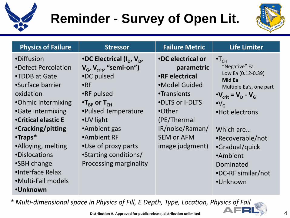
Reminder - Survey of Open Lit.
Physics of Failure Stressor Failure Metric Life Limiter
•DC Electrical (ID, VD, VG, Vcrit, “semi-on”) •DC pulsed •RF •RF pulsed •TBP or TCH •Pulsed Temperature •UV light •Ambient gas •Ambient RF •Use of proxy parts •Starting conditions/ Processing marginality
•DC electrical or parametric •RF electrical •Model Guided •Transients •DLTS or I-DLTS •Other (PE/Thermal IR/noise/Raman/SEM or AFM image judgment)
•TCH “Negative” Ea Low Ea (0.12-0.39) Mid Ea Multiple Ea’s, one part •Vcrit = VD - VG •VG •Hot electrons
Which are… •Recoverable/not •Gradual/quick •Ambient Dominated •DC-RF similar/not •Unknown
* Multi-dimensional space in Physics of Fill, E Depth, Type, Location, Physics of Fail
5 Distribution A. Approved for public release, distribution unlimited
New Doors Opened (NDO)
1. Ratio of Power Density (W/mm) to bulk thermal conductivity (W/m/K):
– Example: About 2.5x greater for GaN vs GaAs. – Concern: Nonlinear effects increase vs. “legacy” power density. – Resolution: A clear path for modest de-rating exists.
• Modeled “True” Peak Temperature • Tch = Tbp + fn(P, Tbp) – Std. Spec Sheet T
Heat source at pinch off Heat source at open channel
S G D
HiREV 60 K
6 Distribution A. Approved for public release, distribution unlimited
New Doors Opened (NDO)
2. Power Density (W/mm) and lots of hot carriers: – Example: About 10x greater W/mm for GaN vs GaAs. – Concern: Open door for multi-electron, multi-phonon effects, more CHC stress. – Resolution: With application specific awareness and modern parts, appears
manageable.
Matteo Meneghini et al., "Degradation of AlGaN/GaN high electron mobility transistors related to hot electrons", Appl. Phys. Lett. 100, 233508 (2012)
Mitigation Options: - Test/Limit at Q point or max PE point as long as possible at highest Vd. Back down Vd for application. - Build in robustness to parametric shifts and/or perform burn-in.
Marco Silvestri, Michael J. Uren, and Martin Kuball, "Dynamic Transconductance ispersion Characterization of Channel Hot-Carrier Stressed 0.25-μm AlGaN/GaN HEMTs", IEEE ELECTRON DEVICE LETTERS, VOL. 33, NO. 11, NOVEMBER 2012.
7 Distribution A. Approved for public release, distribution unlimited
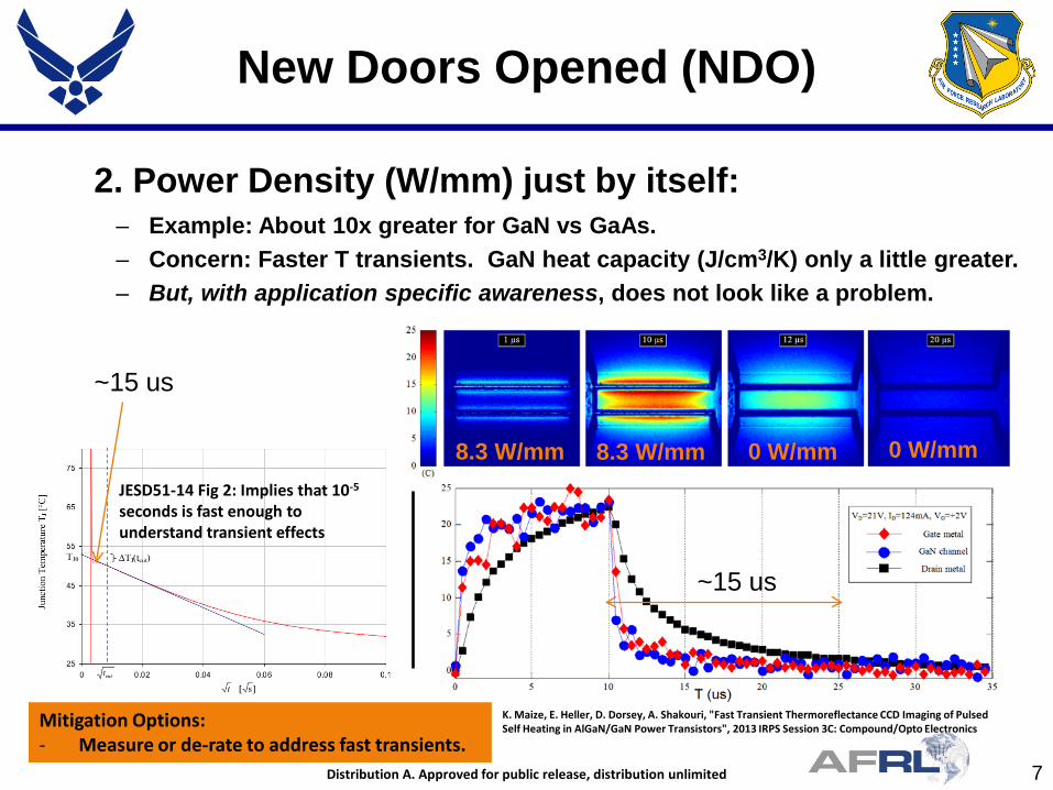
New Doors Opened (NDO)
2. Power Density (W/mm) just by itself: – Example: About 10x greater for GaN vs GaAs. – Concern: Faster T transients. GaN heat capacity (J/cm3/K) only a little greater. – But, with application specific awareness, does not look like a problem.
K. Maize, E. Heller, D. Dorsey, A. Shakouri, "Fast Transient Thermoreflectance CCD Imaging of Pulsed Self Heating in AlGaN/GaN Power Transistors", 2013 IRPS Session 3C: Compound/Opto Electronics
JESD51-14 Fig 2: Implies that 10-5 seconds is fast enough to understand transient effects
8.3 W/mm 8.3 W/mm 0 W/mm 0 W/mm
~15 us
~15 us
Mitigation Options: - Measure or de-rate to address fast transients.
8 Distribution A. Approved for public release, distribution unlimited
NDO: Process Stresses
Mitigation Options : - Fortunately, GaN HEMTs appear robust. - Beware performance boosting tricks, or the sudden appearance or change in processing conditions of overlayer. - Test/Limit extreme abs(Vd – Vg) bias at extremes of ambient temperatures, especially at low T.
3. Late Materials & Process Changes This is an evolving materials system!
Example: Diamond substrate for higher power density But, thermal gradients in GaN are proportional to P density, and commonly cited as a defect migration driver
Example: Strained SiN is a big hit in Si world Tried in GaN (open lit): likely to add new fail modes Many other metastable possibilities exist with energetic processes: MOCVD, MBE, implants, etc.
9 Distribution A. Approved for public release, distribution unlimited
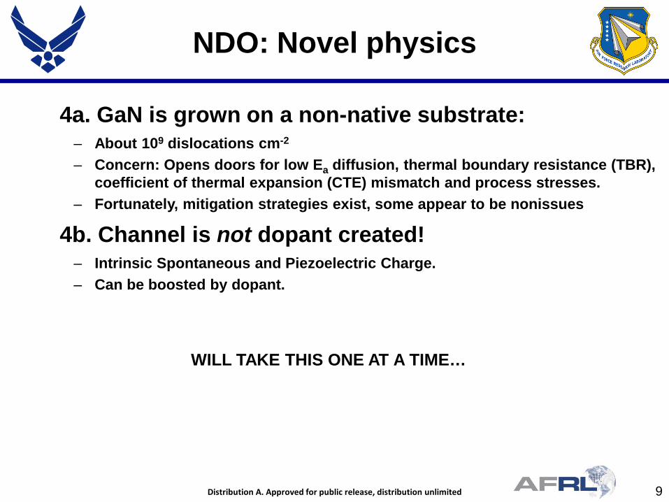
NDO: Novel physics
4a. GaN is grown on a non-native substrate: – About 109 dislocations cm-2 – Concern: Opens doors for low Ea diffusion, thermal boundary resistance (TBR),
coefficient of thermal expansion (CTE) mismatch and process stresses. – Fortunately, mitigation strategies exist, some appear to be nonissues
4b. Channel is not dopant created! – Intrinsic Spontaneous and Piezoelectric Charge. – Can be boosted by dopant.
WILL TAKE THIS ONE AT A TIME…
10 Distribution A. Approved for public release, distribution unlimited
NDO: Extra Thermal Boundary Resistance (TBR)
Martin Kuball et al., "Benchmarking of Thermal Boundary Resistance of GaN-SiC Interfaces for AlGaN/GaN HEMTs: US, European and Japanese Suppliers", CS MANTECH Conference, May 17th-20th, 2010, Portland, Oregon, USA
Red line: Equates to 2.5W/m/K bulk thermal conductivity at 250 °C (assuming 100nm thick)
S G D S G D
4.5 W/mm 4.5 W/mm
Mitigation Options : - Increased T scales as power (W/mm). Use same or less as ALT. Use true worst cast RTH if boosting power past ALT. - Beware process changes to thinner GaN or different epi vendor. DISLOCATIONS ARE LIKELY HERE TO STAY!
With Kuball’s Thermal Boundary Resistance
With Low Thermal Boundary Resistance
Without TBR With TBR
HiREV
HiREV
11 Distribution A. Approved for public release, distribution unlimited
NDO: High Dislocation Density
M. Kuball, Milan Tapajna, Richard J.T. Simms, Mustapha Faqir, and Umesh K. Mishra, “AlGaN/GaN HEMT device reliability and degradation evolution: Importance of diffusion processes” Microelectronics Reliability 51 (2011) pp. 195–200.
Nicola Trivellin, Matteo Meneghini, Gaudenzio Meneghesso, Enrico Zanoni, Kenji Orita, Masaaki Yuri, Tsuyoshi Tanaka, and Daisuke Ueda, "Reliability analysis of InGaN Blu-Ray laser diode", Microelectronics Reliability 49 (2009) 1236–1239.
“showed thermal activation energies of ~0.26 eV consistent with diffusion processes along dislocations, with possible additional contributions from bulk diffusion accelerated by converse/inverse piezo-electric strain and leakage currents.”
GaN laser diode “thermal Activation Energy has been extrapolated to be equal to 250 meV”
Mitigation Options : - Long term testing. As long as possible. ALT for 10,000 hours has been done. - Beware process changes increasing dislocation density, adding more oxygen or other impurities. - Limit Vd and Vg; Select for lowest Ig leakage devices. Expect high dependence on process.
Fail mode often sqrt(time) diffusion blamed again
Low Ea Diffusion?!
Dislocations? Not in active region but in other places!
12 Distribution A. Approved for public release, distribution unlimited
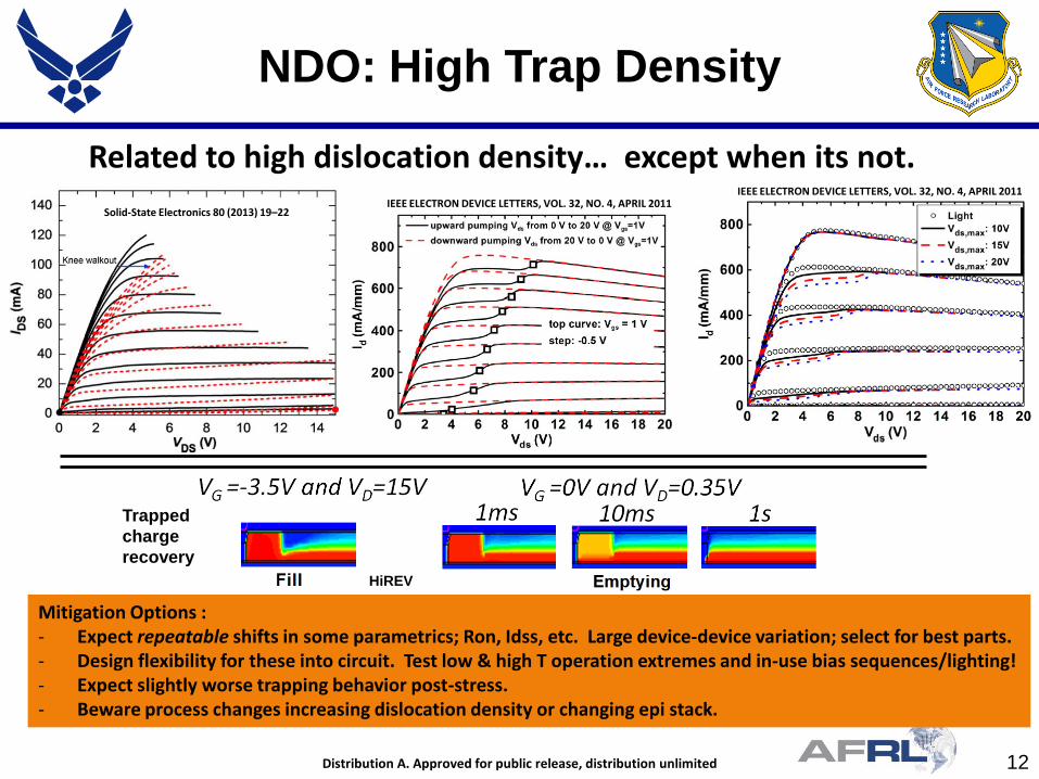
NDO: High Trap Density
Mitigation Options : - Expect repeatable shifts in some parametrics; Ron, Idss, etc. Large device-device variation; select for best parts. - Design flexibility for these into circuit. Test low & high T operation extremes and in-use bias sequences/lighting! - Expect slightly worse trapping behavior post-stress. - Beware process changes increasing dislocation density or changing epi stack.
IEEE ELECTRON DEVICE LETTERS, VOL. 32, NO. 4, APRIL 2011
Related to high dislocation density… except when its not. Solid-State Electronics 80 (2013) 19–22
IEEE ELECTRON DEVICE LETTERS, VOL. 32, NO. 4, APRIL 2011
HiREV
Trapped charge recovery
13 Distribution A. Approved for public release, distribution unlimited
NDO: Substrate Coeff. of Thermal Expansion (CTE) mismatch
Mitigation Options : - GaN HEMTs appear robust to normal cycling. - Test and/or Limit on/off thermal cycling at extremes of storage and use cases. Include power cycling.
Sukwon Choi, Eric Heller, Donald Dorsey, Ramakrishna Vetury, and Samuel Graham, "Analysis of the residual stress distribution in AlGaN/GaN high electron mobility transistors", J. Appl. Phys. 113, 093510 (2013).].
Deflections exaggerated 25x
At 300 C Au Gate
SiN SiN GaN
At 27 C
HiREV
14 Distribution A. Approved for public release, distribution unlimited
NDO: Origin of Channel Charge
• Channel is not Dopant Defined: – Due to intrinsic spontaneous and piezoelectric charge in bulk AlGaN and GaN – Arises from change in bulk material properties at interface – Good points: No dopant freeze-out, process variation in dopant density, no
concerns of dopant passivation, migration of ionized scatterers to channel, etc. – Concern: Charge in the channel is very sensitive to AlGaN thickness, mole
fraction, mechanical stress, or changes thereof. – Resolution: Process control, understand variation, avoid process cliffs. Even a
small increase in AlGaN thickness/mole fraction may induce new failure modes!
Mitigation Options: - Fortunately, largely a non-issue. - Beware potentially metastable performance boosting tricks (novel stress incorporating layers, etc). - Exploit within-wafer variation for rel: select for parts with lower AlGaN mole fraction or thickness. - Test/Limit extreme Vd - Vg at extremes of ambient temperatures, especially low T. Select for lowest Ig leakage.
15 Distribution A. Approved for public release, distribution unlimited
New Doors Opened (NDO)
• 5. Wide Bandgap (eV): – Example: About 2.5x for GaN vs GaAs. – Very hot electron effects, holes carry a lot of energy, – Semi-infinite trap lifetimes, especially when cold. – Workhorse tool DLTS will not measure the deeper traps at room T. – Concern: Deeper traps, and semi-infinite thermal resets. – Resolution: Application specific awareness.
Mitigation Options : - De-rate for Vd. Fortunately technology has a lot a margin to de-rate. - Yet, high Vd can reset traps & mask an issue! Verify system operates cold and at lowest allowed Vd operation. - Verify low & high T operation in the dark, especially circuit corners in Vt, near Vt device operation, low Vd
operation, and low Vd operation just after the coldest, most extreme high Vd at hard pinch-off for in-use.
16 Distribution A. Approved for public release, distribution unlimited
New Doors Opened (NDO)
• 6. High critical breakdown field (V/cm): – Example: About 8x greater for GaN vs GaAs. – Concerns: Very high E fields, very hot electron effects, not accelerated
thermally, drift by E field of charged traps, high inverse PZ mech. stresses! – Channel noise, Ig noise, and Ig leakage changes. – Resolution: GaN is tough! With awareness, may not be an issue.
Mitigation Options : - Can de-rate for Vd. Technology has a lot a margin to de-rate by. Select for lowest Ig leakage parts. - High Vd, high Abs(Vd-Vg) can supply energy to fail modes. Test high Abs(Vd-Vg) at low/high T. - Select lowest Ig parts. Might use low/high Ig as an ALT “stressor”, with increase in Ig, Ig noise as fail metric. - Watch for cratering (esp. on test)! High Vd means that system capacitances can feed energy as Vd^2! - Not expected to be an issue for RF devices at nominal Q point.
Matteo Meneghini et al., "Time-dependent degradation of AlGaN/GaN high electron mobility transistors under reverse bias" Appl. Phys. Lett. 100, 033505 (2012).
Congyong Zhu et al., "Reduction of Flicker Noise in AlGaN/GaN-Based HFETs After High Electric-Field Stress", IEEE ELECTRON DEVICE LETTERS, VOL. 32, NO. 11, p. 1513, NOV. 2011. Stress was
Vgs = 0V, Vds = 20 V
17 Distribution A. Approved for public release, distribution unlimited
Switching Gears
• We want a well defined Physics of Failure, Stressor(s), Fail Metric(s) (like Si CMOS)
Well defined “path” to follow for reliable conclusions
This time its… Col. Mustard, In the Study, Lead pipe.
18 Distribution A. Approved for public release, distribution unlimited
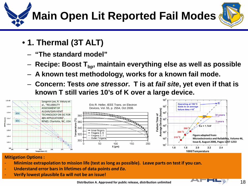
Main Open Lit Reported Fail Modes
• 1. Thermal (3T ALT) – “The standard model” – Recipe: Boost Tbp, maintain everything else as well as possible – A known test methodology, works for a known fail mode. – Concern: Tests one stressor. T is at fail site, yet even if that is
known T still varies 10’s of K over a large device.
Mitigation Options : - Minimize extrapolation to mission life (test as long as possible). Leave parts on test if you can. - Understand error bars in lifetimes of data points and Ea. - Verify lowest plausible Ea will not be an issue!
Sangmin Lee, R. Vetury et al., "RELIABILITY ASSESSMENT OF ALGAN/GAN HEMT TECHNOLOGY ON SIC FOR 48V APPLICATIONS", RFMD, Charlotte, NC, USA
Figure adapted from: Microelectronics and Reliability, Volume 46, Issue 8, August 2006, Pages 1247-1253
Eric R. Heller, IEEE Trans. on Electron Devices, Vol. 55, p. 2554, Oct 2008.
19 Distribution A. Approved for public release, distribution unlimited
Main Open Lit Reported Fail Modes
• 2. Channel Hot Carrier (CHC) Stress – High E field near pinch-off with some electrons – Initial (Time=0) IDSS and CHC effect correlation seen. – NOT the highest power point. – NOT very thermally accelerated if at all! – Knowable test methodology.
• Run as highest Vd near Q point or peak PE point.
– Concern: Peak stress point is how we want to run an RF device!
Mitigation Options : - Minimize extrapolation to mission life (test as long as possible) - Test at highest mission Vd at or near Q point and/or at or near highest PE point. - Keep track of Idss, select for application accordingly.
20 Distribution A. Approved for public release, distribution unlimited
Main Open Lit Reported Fail Modes
• 3. “Critical Field” Failure – Past the critical Abs(Vd-Vg), instantaneous – Near the critical Abs(Vd-Vg), minutes/hours – High Abs(Vd-Vg) via extreme negative Vg IS NOT the same as
high Abs(Vd-Vg) via extreme positive Vd at deep pinch-off. – Recipe: Apply high Abs(Vd-Vg); Vd at extreme positive values at
deep pinch-off. – The good: Quick, easy test methodology. Easy to build test
channels. Don’t have to consider thermal issues much at test.
Mitigation Options : - Not usually an issue; biases usually far from RF HEMT application conditions. - Test for hours. Test at both lowest and highest mission T. - Watch Ig, changes in Ig and photoemission (if possible) and Ig noise as a prelude to failure. - Correlated to Ig leakage at time = 0; select for lowest Ig, low Ig noise parts. - Might use low-high Ig time = 0 parts as an alternate “stressor”
21 Distribution A. Approved for public release, distribution unlimited
Further thoughts: Traps and Transients!
• Lots of considerations – Intrinsic, very process dependent, light sensitive, usually resettable – Transient Recovery after high Vd, high power RF or pinch-off point.
“Current slump”, “gate lag”, “virtual gate”, RON and VTH affected, etc. – More problematic in general at low T, and not the highest power point. – Can get worse with stress or end of life (usually not much) – Can trigger a “failed part” decision. Typically 10% Idss or 1dB – Recipe: watch transient after a “pulse” of some sort. – Fortunately, non-destructive test methodologies exist. – Concern: Horrible to model*, can’t characterize them directly.
Mitigation Options : - Test at both lowest mission T, right after “worst transients”*. Think of highest T too. - *How long does the part deviate from acceptable operation after a high Vd, high power RF or pinch-off point? - Select for least affected parts after “worst transients” and build in margin for these transient issues. - Back down “trap setting” events as much as possible, and consider future bias states post trap setting events. - Can be reset by light, T and hot electrons; have a UV GaN LED, dummy heater, or hot electron “panic” option?
*function of density, location, energy depth, several traps cited in same place at same time, can be resettable or not, etc.
22 Distribution A. Approved for public release, distribution unlimited
Further thoughts: “Grooves”, “Cracks” and “Pits”!
• Causes attributed to – Thermal – Nonthermal - High power generated – Nonthermal - High electric field generated
• Instant (high Inv. PZ mechanical) or gradual. S and/or D side of G • Much debate on if this is a fail mode or a nuisance! RON and IDMAX appear most affected.
Jungwoo Joh, Jesús A. del Alamo, "Impact of gate placement on RF power degradation in GaN high electron mobility transistors", Microelectronics Reliability 52 (2012) 33–38.
S.Y. Park, "Physical degradation of GaN HEMT devices under high drain bias reliability testing", Microelectronics Reliability 49 (2009) 478–483.
23 Distribution A. Approved for public release, distribution unlimited
Why are we not done?
A. Sozza et al., Microelectronics Reliability 45 (2005) 1617–1621
BIN 1. MATERIALS/PROCESS IMMATURITY
• Large variation in degradation rate of nominally “identical” parts. - A “fog” that cuts across industry. Rapidly getting better!
• Much larger variation across processes! - Secrecy/Proprietary limits sharing Limited distributions of new parts Process details, origin of parts often unknown - “Cutting edge” conclusions drawn from old or marginal parts! HiREV University Foundry run.
If we had the luxury of starting from scratch… - Use modern parts - Minimize sharing restrictions for academic research - Verify findings with multiple vendors
24 Distribution A. Approved for public release, distribution unlimited
Why are we not done? BIN 2. TEST AND FAILURE ANALYSIS IMMATURITY • Large variation in test protocols
- Rth: IR thermal, micro-Raman, modeling - Random tested population or cherry-picked? - Each data source explores a subset of stressor par space. HiREV role as independent tester facilitating uniform testing HiREV working full statistical understanding of problem
• Failure Analysis is mostly “find once and report”, not protocol development
- Very few “findings” use a closed loop approach (pre-post stress) - Little said on how the “found” defect is known to be the “real” defect! HiREV working to cross-correlate FA findings and close the loop
If we had the luxury of starting from scratch… - Compare/set test protocols early - Compare/set Failure Analysis protocols early - Fully document for full reproducibility!
25 Distribution A. Approved for public release, distribution unlimited
Why are we not done? BIN 3. THE UNDERLYING PHYSICS HAS CHANGED
• Very large peak E fields, temperatures, thermal gradients. - Can make “nonstandard” drivers relevant. - Complex interplays cited in literature (i. e. drifting charged point traps). -Can require coupled mechanical/thermal/electrical physics.
- Awareness of this complexity is now critical! - Adequacy of existing test channels and test methodology? HiREV working fundamental science and tool assessment HiREV working full understanding of the “stressor space”
• Traps, traps, traps
- Nearly impossible to directly measure, yet a genuine issue. - Easy to cite, hard to quantify: density, location(s), species, conditions. - High dislocation density, probably here to stay - Wide bandgap: means traps have microseconds to many days lifetime. This will require closure. Verification/Validation Critical. HiREV working to directly quantify traps under the gate (expt. & model)
26 Distribution A. Approved for public release, distribution unlimited
Conclusions and Final Thoughts
• Many Deltas in Physics from Legacy Materials • Most relate to fact that GaN can be pushed harder than prior materials. • Some are intrinsic to the new materials system.
• Understand your application! • Literature has found a few main mechanisms.
• Classic thermal “3T ALT” wear-out. The one you were warned about! • Channel Hot Carrier (CHC) stress • High Voltage “critical field” failures.
• Traps can be thought of as a fourth failure mode but many characteristics differ from other modes.
• Last, discussion of why we don’t have firm fail models in place & how to address these concerns.
27 Distribution A. Approved for public release, distribution unlimited
SUPPLEMENTAL
28 Distribution A. Approved for public release, distribution unlimited
Example: HiREV Thermal Characterization
IR Thermography • Quick look at heating uniformity • Good for part-part variation • Not good for absolute temperatures •~3-5 µm spatial resolution
µRaman • Accurate point thermometry • 1 µm spatial resolution • Mapping possible • Measures GaN or SiC temperature only; optical access limitations
Thermoreflectance • Transient measurement with 50ns resolution • Submicron spatial resolution • Full device imaging • Surface localized
Electro-Thermal Modeling • Thermal Transients • Best spatial resolution • Full device to package • Buried not an issue • Only as good as input data lots of validation!
29 Distribution A. Approved for public release, distribution unlimited