Network Intrusion Detection Systems on FPGAs with On-Chip Network Interfaces Christopher Clark Georgia Institute of Technology Craig Ulmer Sandia National Laboratories, California Craig Ulmer [email protected]February 22, 2005 Sandia is a multiprogram laboratory operated by Sandia Corporation, a Lockheed Martin Company, for the United States Department of Energy’s National Nuclear Security Administration under contract DE-AC04-94AL85000.
Transcript
Network Intrusion Detection Systems on FPGAs with On-Chip Network Interfaces
Christopher Clark Georgia Institute of TechnologyCraig Ulmer Sandia National Laboratories, California
Sandia is a multiprogram laboratory operated by Sandia Corporation, a Lockheed Martin Company,for the United States Department of Energy’s National Nuclear Security Administration
under contract DE-AC04-94AL85000.
Network Intrusion Detection Systems on FPGAs with On-Chip Network Interfaces
Note: This work was not performed by SNL’s network security group and is independent of SNL’s network security policy or infrastructure.
Packet
Good
Malicious
NIDS
Chris Clark / Georgia Tech Craig Ulmer / SNL
+
NI
NI
FPGA Network
Outline
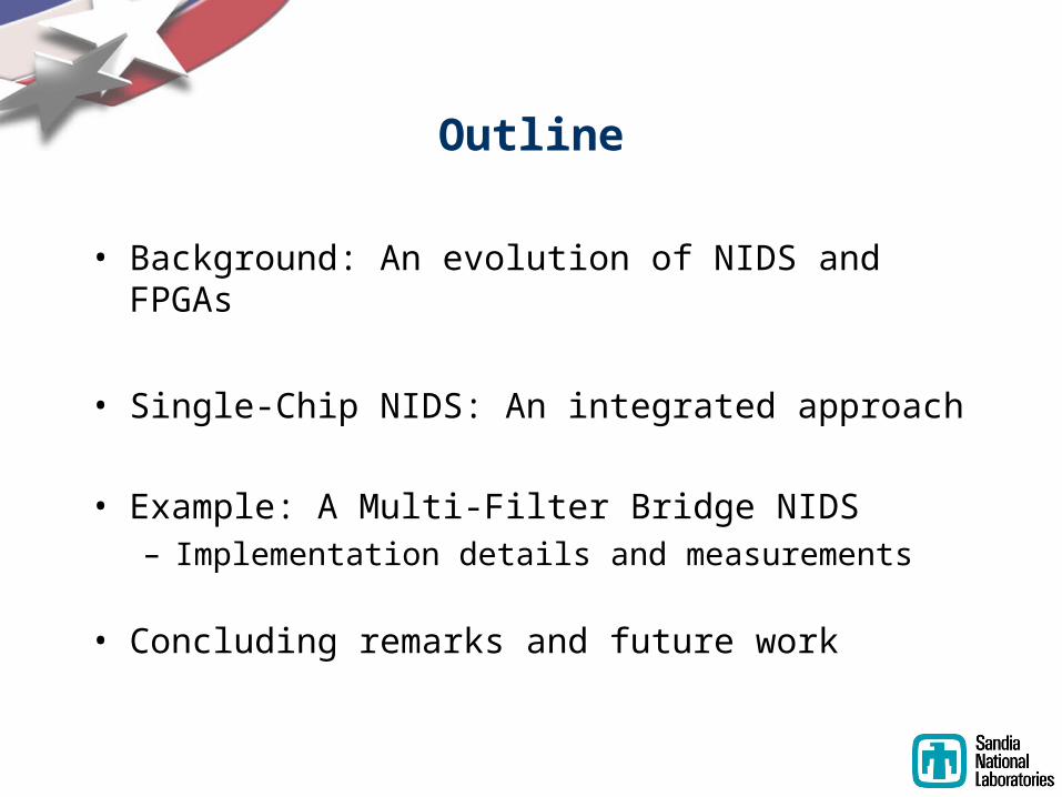
• Background: An evolution of NIDS and FPGAs
• Single-Chip NIDS: An integrated approach
• Example: A Multi-Filter Bridge NIDS– Implementation details and measurements
• Concluding remarks and future work
Background: An Evolution of NIDS and FPGAs
Network Intrusion Detection Systems (NIDS)
• There are many malicious users on the Internet– Unprotected home PCs hijacked within 10 minutes
– Even if protected- still fighting denial of service
• Network Intrusion Detection Systems (NIDS)– Monitor network and react to attacks
• Example: Snort (www.snort.org)– Large database of malicious packet signatures
– 1,305 rules with 1,512 patterns
– Pattern matching on 17,537 characters
Host-based NIDS Implementations
NIC
CPU
NIC
CPU
FPGA
NIC
CPU
FPGA
Software FPGA Card FPGA-enabled NIC
I/O I/OI/O
• Multiple architectures proposed for NIDS– Separation of Network Interface and Intrusion Detection
ID
IDID
Single-Chip NIDS: An Integrated Approach
Evolution: An Integrated Approach
• New FPGAs have network transceivers– FPGAs interact directly with network
• Build complete NIDS in an FPGA– NI and ID units under one roof
• Integration benefits– Customization of units and topology– Portability– New applications
• Describe our integration experiences
NI
NI
Network
FPGA
IntrusionDetection
FPGA
IntrusionDetection Network
NetworkInterface
Chip
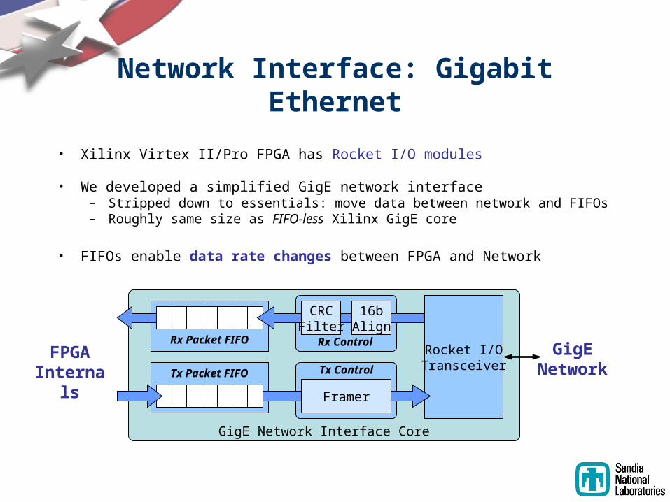
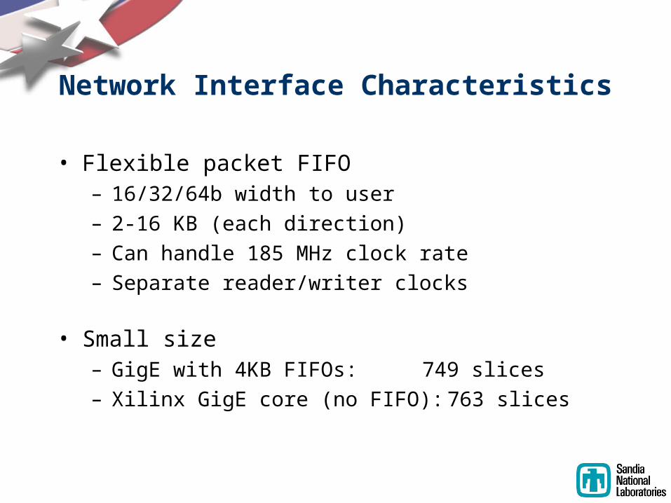
Network Interface: Gigabit Ethernet
• Xilinx Virtex II/Pro FPGA has Rocket I/O modules
• We developed a simplified GigE network interface– Stripped down to essentials: move data between network and FIFOs– Roughly same size as FIFO-less Xilinx GigE core
• FIFOs enable data rate changes between FPGA and Network
Rx Control
Tx Control
Rx Packet FIFO
16bAlign
CRCFilter
Tx Packet FIFO
GigE Network Interface Core
Rocket I/OTransceiver
GigENetwork
Framer
FPGAInternals
Intrusion Detection Unit
HeaderDecoder
HeaderAnalysis
Header
PayloadAnalysis
MatchDecision
Logic
Drop
Match
Match Vector
EthernetFrameData
• Snort rules translated to structural JHDL intrusion detection unit– Compile time select 16/32/64b data width– Both header/payload analysis units
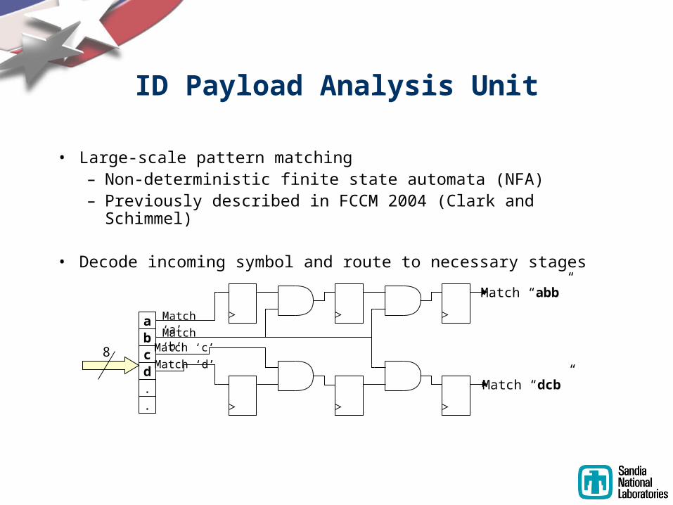
• Payload analysis unit performs large-scale pattern matching– Non-deterministic finite state automata (NFA)– Previously described in FCCM 2004 (Clark and Schimmel)
AlignedPayload
PayloadMatch
HeaderMatch
Integrated Example: A Multi-Filter Bridge NIDS
Filtering Network Connections
• Desire a NIDS that we can insert on a network link– Detect and filter out attacks
– Transparent to users
– Single bi-directional link: Filter Bridge
– Can extend to support multiple filter bridges per FPGA
NI NI
ID Unit
FPGA
Single Filter Bridge
NI NI
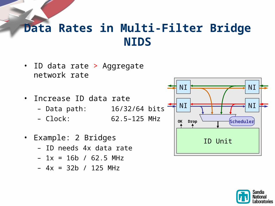
Data Rates in Multi-Filter Bridge NIDS
• ID data rate > Aggregate network rate
• Increase ID data rate– Data path: 16/32/64 bits
– Clock: 62.5–125 MHz
• Example: 2 Bridges– ID needs 4x data rate
– 1x = 16b / 62.5 MHz
– 4x = 32b / 125 MHz
ID Unit
NI NI
OK Drop Scheduler
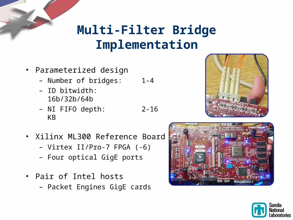
Multi-Filter Bridge:Implementation Details and Measurements