27
New Inspection Solution for Probing Technology Clark Liu Tim Yang PTI Taiwan
New Inspection Solution for Probing Technology
Clark LiuTim Yang
PTI Taiwan

Clark Liu / Tim Yang
Overview • Background / Introduction• Inspection Solution for Probing Technology
(1)In Line Inspection Solution : AOI / Prober (2)Off Line Inspection Solution : Probe Card AOI / 3DMS
• Future Work for the Inspection Solutions • Conclusions• Acknowledgement
2

Probing Inspection
“ To Be , or not to Be :That is a Question! ”
Clark Liu / Tim Yang 3

(1) Usually, Test Hourly Rate not include Full Inspection Cost!
Test Cost just cover minimum inspection investment!
(2) The Inspection Technology must cover the Probing Quality Control as
KGD / Zero Defect Business!
(3) Reasonable Inspection cost could keep driving Probing Technology Continue
Improvement Progress and DFM!
Background: Cost is Key!
Clark Liu / Tim Yang 4

Introduction: New Inspection Solution for Probing Technology
• The Probe and Probe Mark Quality Control were Key Issues for Wafer Level Package Probing Technology. How to measure the Probe and Probe Marks from in-line and off-line tools will discuss at this presentation.
• We development the new tools for probe card /probe mark inspection. New tools provide more efficiency data for clearly engineering information and related setup issues.
• We believe the New Inspection Solution could more helpful from user and supplier and improve the probing technology. Will share relate information with partners .
Clark Liu / Tim Yang 5

6
WLCSP RDL CPB
Nee
d O
ff Li
ne
Insp
ectio
n Li
ghtly
P/M
I
New Inspection Solution
Requirement
Why Need Inspection for WLP Probing Technology
Consider for both I/F Probe and Material as Quality Requirement from KGD and Zero Defect Requirement.
PAD
P/ M
<25%
,
No
Punc
h th
roug
h
Clark Liu / Tim Yang

Inspection Requirement in Probing Technology
In Line Inspection
Wafer Probe Card
Off Line Inspection
Quality
Cost
YieldDelivery
Clark Liu / Tim Yang 7

Wafer and Probe Card Inspection Process Flow
Wafer IQC Lab AnalysisWafer:
Prober In Line Check
Wafer OQC Eng
Time PressureReal Time
Probe Card IQC
Lab Analysis(Head Size?)
Probe Card Prober In
Line Check
Probe Card OQC Eng
Wait for Long Time
Clark Liu / Tim Yang 8
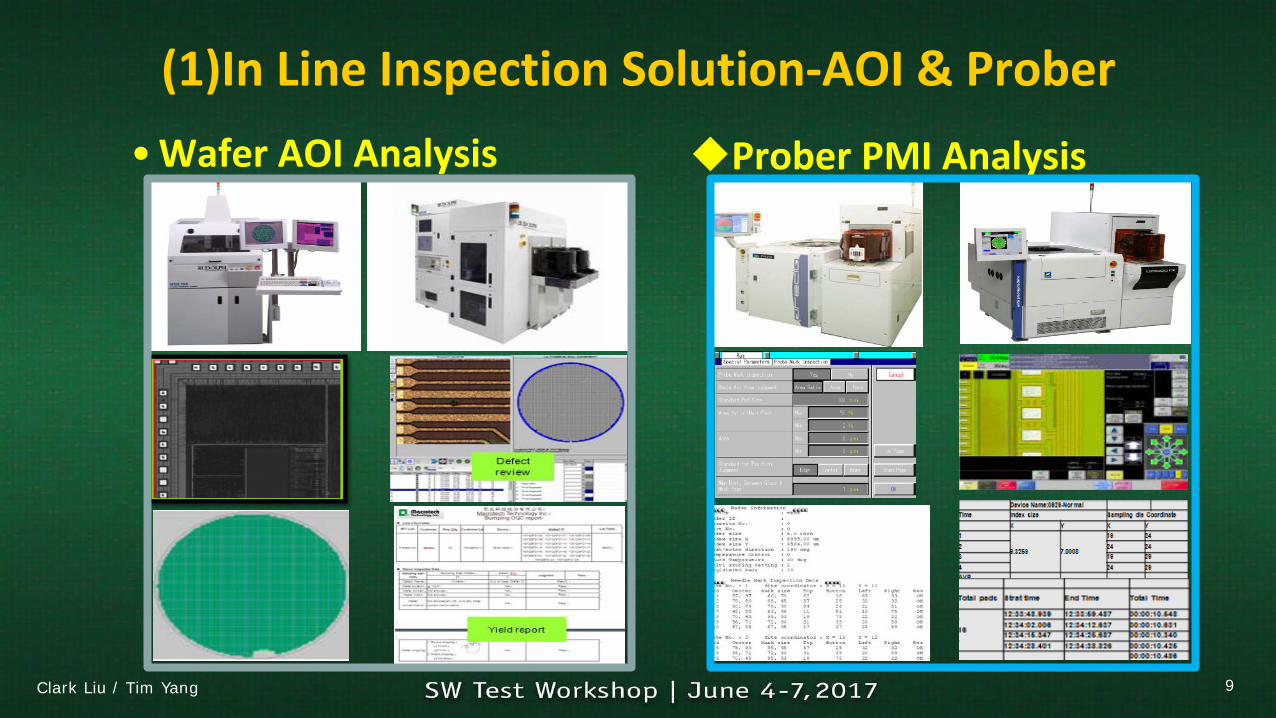
(1)In Line Inspection Solution-AOI & ProberProber PMI Analysis• Wafer AOI Analysis
Clark Liu / Tim Yang 9

Wafer center is under control
Wafer edge get Worst need special Set Up
Probe Mark Shift in Spec but the means get shift
AOI Probe Mark Analysis for 2 TD Probe card Set Up :
Clark Liu / Tim Yang 10
KGD Challenges : 2TD P/C for Probe Mark Area and Keep Out Control
Probe Mark A/A <25%Production P/M Keep Out
>5um
Production P/M Keep Out <5um
(Vender only ensure Off Line Check @RT >5um)
Probe Mark A/A <25%Production P/M Keep Out
>5um

More Data to Analysis
Clark Liu / Tim Yang 11
ProberSetup / System
A xxx Analysis
Set Up Issue
Probe Mark Issue
Probe Card Issue
Prober In Line Check
Probe Mark& Probe
SystemIssue
AlignmentIssue
Card Holder/Docking Issue
RecipeIssue
NxxxAnalysis
Special Setup
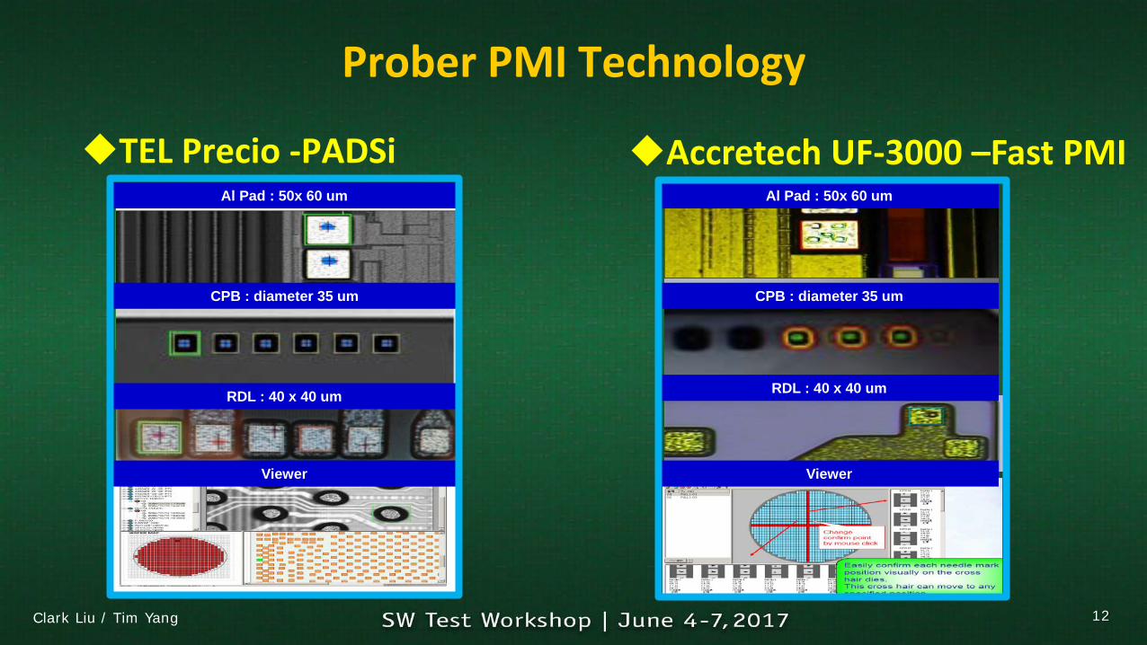
Prober PMI Technology
TEL Precio -PADSiAl Pad : 50x 60 um
CPB : diameter 35 um
RDL : 40 x 40 um
Viewer
Accretech UF-3000 –Fast PMIAl Pad : 50x 60 um
CPB : diameter 35 um
RDL : 40 x 40 um
Viewer
Clark Liu / Tim Yang 12

In Line Challenge: AOI and Prober for RDL Probe mark Inspection
AOI
[Issue]: 1. Customer Spec: Not allow probing out of RDL
Pad.2. AOI and Prober both can detect the Probe Mark
under the RDL Pad or Not. But could not identify the Clearly P/M size with OD! That will hard to check the setup issue!
3. Probe mark Inspection Analysis Technology still need vender support to development.
Prober
Clark Liu / Tim Yang 13

PastThinking
NEWThinking
(2)Off Line Check Solution : AOI / 3DMS Technology
2.1
2.2
Clark Liu / Tim Yang 14
$
∮
Probe Card Checker
SEMSEM OM
AOI Probe card Checker
3DMS

(2.1)AOI System Development Concept for Probe Card
Probe CardChecker
(1)T/P Higher(2)Cost Lower
Probe Mechanical
(1)Need Different ATE M/B
AOI CheckProbe Card
Clark Liu / Tim Yang 15
(3)In Line ATE-Wafer check outMeasure
Probe Electrical
DC
Probe Electrical
AC
(2)Different P/C need Change Different M/B and Setup Time
Probe Mechanical
Probe Electrical
DCProbe
Electrical AC
(5)In Line ATE-Wafer check outMeasure
(1) No need M/B(2) Less Setup time
(3) Real Time Photos(4) High Accuracy
Equal In Line T/T

(2.1)Probe card Measurement _ AOI Solution
Probes (X,Y,Z ) / Probe Head Data Probe Pictures
Clark Liu / Tim Yang 16
(1) No Limited for Exist ATE P/C
(2) High T/P(3) High Accuracy

Probe Cards AOI Checker SolutionNo Need Any Mother Board
uFlex-DD Card93K-DD Card
T5377s-Full Contact Card T5593 KGD Card
Clark Liu / Tim Yang 17

2016 SWTW :Trying make 3D Microscope for WLP / Probe card
Engineering Analysis
3D_RDL
CPB(x5000)
Al Pad
3D_Pogo Top
3D_Probe
2D_RDL
Development for Wafer and Probe card
Inspection
Clark Liu / Tim Yang 18
(1) No Limited for Measure
(2) High Accuracy like SEM
(1) Try & Error for CIP(2) Need more times
to developthis system

(2.2)New Inspection System Development Concept for Probe Card and Wafer
Wafer IQC
3DMS Analysis
Prober In Line Check
Wafer OQC(1)Short Lead Timein Probing Line
Time Pressure
Probe Card IQC
Prober In Line Check
Probe Card OQC
(3)No Limited for Measure
Clark Liu / Tim Yang 19
(2)High Accuracyfor Measure Equal as SEM
(4)Fast Validate Probe and Probe Mark Contact Relate Result
Targets

2D/3DMS for Al Pad Probe mark
2DMS: Probe Mark Inspection3DMS: Probe Tip /Probe Mark Depth
Vender A Vender B
Clark Liu / Tim Yang 20

3DMS check for Probe and Bump
10um
• Probe tip – Geometry / Debris • Probe Depth Measurement
Clark Liu / Tim Yang 21

2D/3DMS finding for Probe Lifetime
• 2DMS- Probe Diameter/ Height-Probe Wearing Issue
• 3DMS-New Finding-+ Membrane Structure Issue
Clark Liu / Tim Yang 22

3DMS for All P/Cs and Devices forEngineering Analysis Capability
Flexible for Different Type P/Cs and Devices
uFlex P/C
T537X P/C
93K P/C
P/C Type
300mm Wafer Sub Panel
PAD
WLCSP
DevicesPogo Probe
Membrane Probe
Contact I/F Probe Type
CPB
MEMS ProbeRDLClark Liu / Tim Yang 23

Conclusion
24
Inspection Solution
Business
Share Technology
CommunicationValidationSaving Cost
MFG Technology
Shot on Target
New Concept
Time to Market
New Application
Build up the new working model for Customer Service & Probe suppliers! Helpful for Next Step Development!
Clark Liu / Tim Yang
$ ∮
∮
Ω

Future Work: AOI New Function for WLP Probe mark Analysis
25
AOI /3DMSProbing Result
Analysis
User / Customer
ExpectData
WLP I/F Shrink Trend Roadmap , Development Big Data to analysis :(1) Prober Performance(2)Probe card Performance(3)Validate New Probing Technology
Clark Liu / Tim Yang
WLCSP
RDL
CPB
uBump

Tester Prober
Future Work: Many Data Streams for Big Data
Probe Card
Vender OQC Data
Probe Mark WoW OQC Data
Prober PMI Data
3DMS Probe Mark Data
Card Checker Data
3DMS Probe IQC Data
Prober Alignment Data
Prober PADSi Data
Wafer YieldData
Clark Liu / Tim Yang 26

Acknowledgments
We would like to thank PTI colleagues support for this presentation. (1) Henry Tseng(2) Allan Ku(3) James Hsieh
Also thanks suppliers fully support this project.(1) Taiwan Local Suppliers(2) Accretech / Rudolph / TEL
27Clark Liu / Tim Yang
Thank you!


