Page 1
New Requirements for Sir- Measurement
Jörg Trodler
Heraeus Materials Technology GmbHo.KG
Hanau, Germany
[email protected]
Mathias Nowottnick, Prof.
University of Rostock
Rostock, Germany
Abstract
During the last period of newly assembled electrical devices (pcbs), new component types like LGA and QFN were also
qualified as well as smaller passive components with reliability requirements based on the automotive and industrial industry.
In the narrow gaps under components, residues can accumulate more by the capillary forces. This is not that much a surface
resistance than an interface issue. Also that the flux residues under such types of components creates interaction with the
solder resists from the pcb, as well as the component body was not completely described in the standard SIR measurement.
On the other hand also, electrical influence with higher voltage creates new terms and conditions, in particular the
combination of power and logic in such devices. The standard SIR measurement cannot analyze those combinations. The
paper will discuss the requirements for a measurement process, and will give results. The influences of the pcb and
component quality will also be discussed. Furthermore it will describe requirements for nc solder paste to increase the
chemical/thermical/electrical reliability for whole devices.
Introduction
Since the beginning of the Surface Mount Technology there had been created a lot of measurement methods to qualify the
quality/stability of flux residues by using solder paste. That means there are international, national and company standards for
the qualification of that auxiliary material [STD-01]. That qualification gives an initial idea of the quality but unfortunately it
doesn’t give all information for the whole assembly. As an example, in some cases there will be used, on the residues of no
clean flux residues, conformal coating. Each single material passed the qualification according the standards but in
combination with both, it is possible to create failure [Sch-06]. Other points are new types of components (miniaturization)
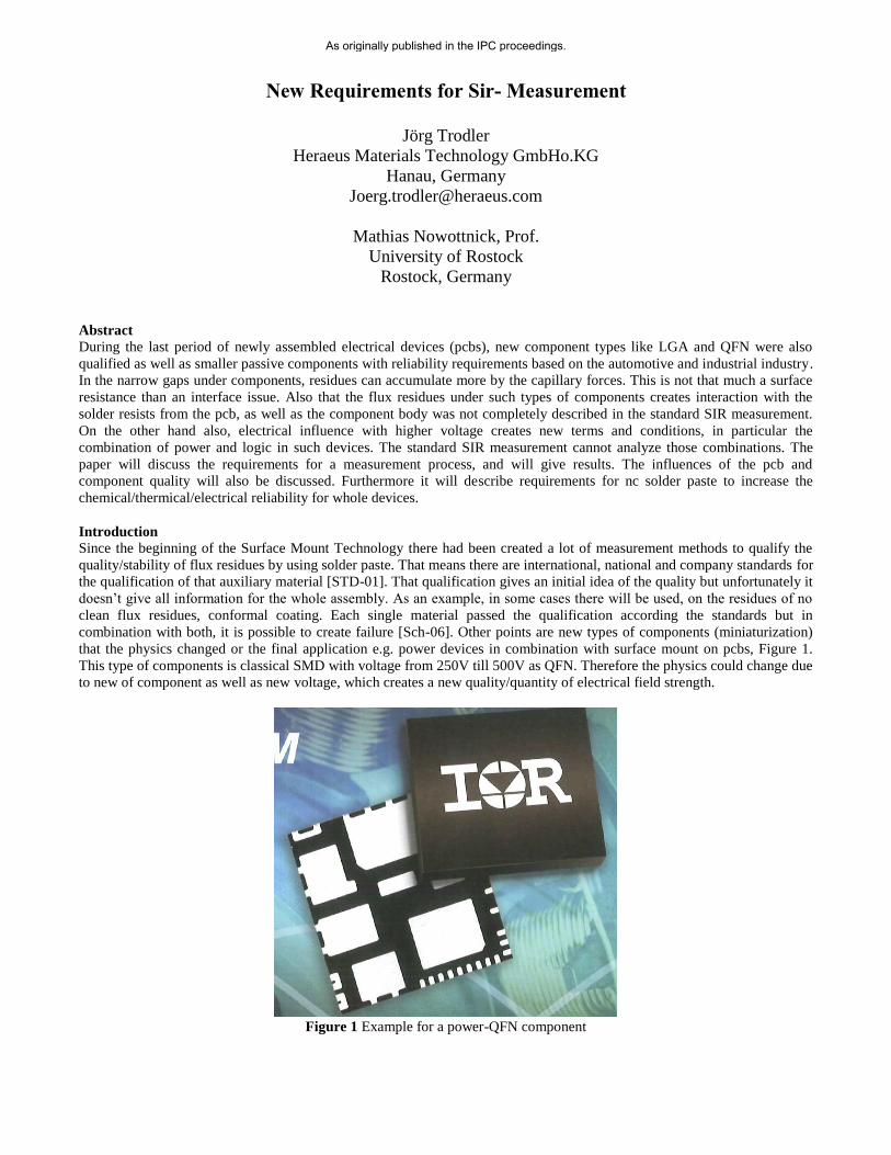
that the physics changed or the final application e.g. power devices in combination with surface mount on pcbs, Figure 1.
This type of components is classical SMD with voltage from 250V till 500V as QFN. Therefore the physics could change due
to new of component as well as new voltage, which creates a new quality/quantity of electrical field strength.
Figure 1 Example for a power-QFN component
As originally published in the IPC proceedings.
Page 2
Another point is the combination of high humidity and voltage. Especially the automotive industry requires that also for
simply devices.
FLUX PENETRATION UNDER COMPONENTS
The standard test methods for measuring effects of fluxes are determining the insulation resistance only on free surfaces. The
actual situation of electronic assemblies is considerably more complex. Among and between components, both the flux, but
also the dewing moisture is concentrated. Depending on the gap height and areas of the components, capillary forces can
effect very different. Because of component designs such as QFN or LGA, these effects are becoming more and more
relevant. Even the cleaning of assemblies is complicated by these small gaps. Perhaps this problem will be intensified even
by cleaning.
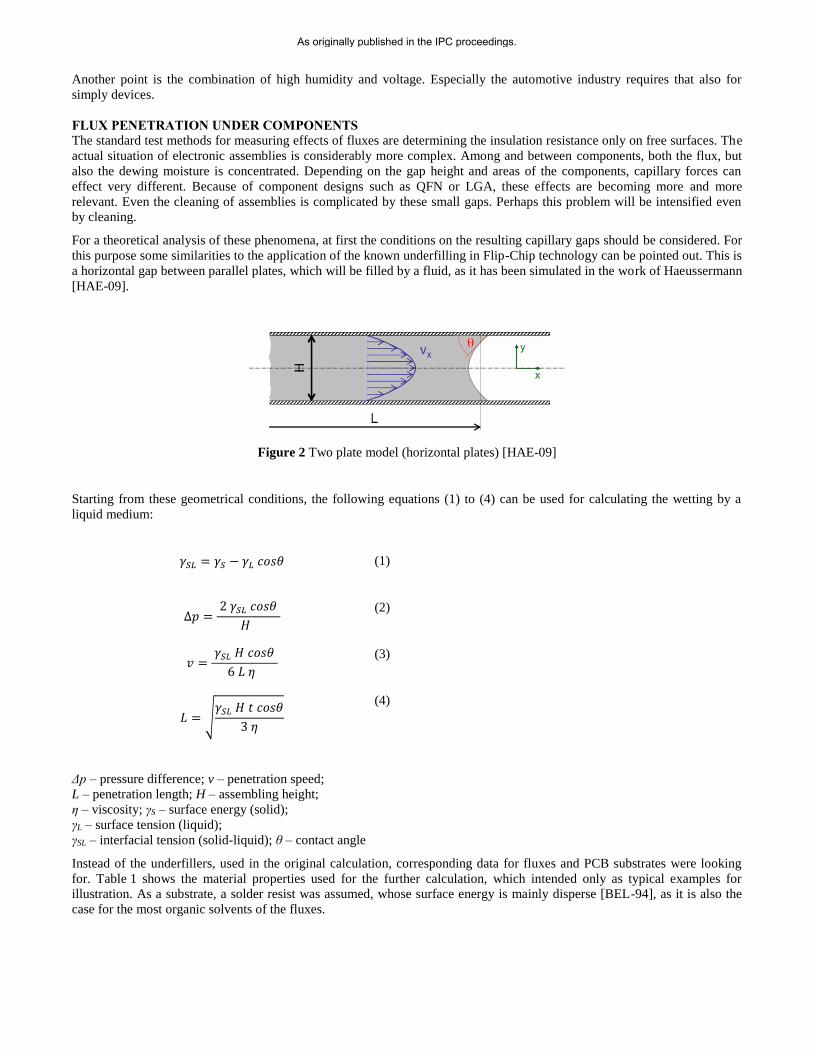
For a theoretical analysis of these phenomena, at first the conditions on the resulting capillary gaps should be considered. For
this purpose some similarities to the application of the known underfilling in Flip-Chip technology can be pointed out. This is
a horizontal gap between parallel plates, which will be filled by a fluid, as it has been simulated in the work of Haeussermann
[HAE-09].
Figure 2 Two plate model (horizontal plates) [HAE-09]
Starting from these geometrical conditions, the following equations (1) to (4) can be used for calculating the wetting by a
liquid medium:
𝛾𝑆𝐿 = 𝛾𝑆 − 𝛾𝐿 𝑐𝑜𝑠𝜃 (1)
∆𝑝 =
2 𝛾𝑆𝐿 𝑐𝑜𝑠𝜃
𝐻
(2)
𝑣 =
𝛾𝑆𝐿 𝐻 𝑐𝑜𝑠𝜃
6 𝐿 𝜂
(3)
𝐿 = √𝛾𝑆𝐿 𝐻 𝑡 𝑐𝑜𝑠𝜃
3 𝜂
(4)
Δp – pressure difference; v – penetration speed;
L – penetration length; H – assembling height;
η – viscosity; γS – surface energy (solid);
γL – surface tension (liquid);
γSL – interfacial tension (solid-liquid); θ – contact angle
Instead of the underfillers, used in the original calculation, corresponding data for fluxes and PCB substrates were looking
for. Table 1 shows the material properties used for the further calculation, which intended only as typical examples for
illustration. As a substrate, a solder resist was assumed, whose surface energy is mainly disperse [BEL-94], as it is also the
case for the most organic solvents of the fluxes.
As originally published in the IPC proceedings.
Page 3
Table 1 Material properties from references (typical examples)
Material Properties Ref.
substrate
surface energy 39 mN/m
WAN-06 contact angle
(flux/mask) 26,2°
alcohol
based
flux
surface
tension 22.6 mN/m
WES-08
viscosity 2.97 mPa*s
flux
cleaner
surface
tension 23 mN/m
CRC-04
viscosity 1.2 mPa*s
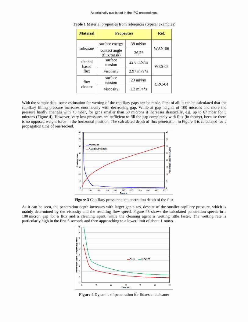
With the sample data, some estimation for wetting of the capillary gaps can be made. First of all, it can be calculated that the
capillary filling pressure increases enormously with decreasing gap. While at gap heights of 100 microns and more the
pressure hardly changes with <5 mbar, for gaps smaller than 50 microns it increases drastically, e.g. up to 67 mbar for 5
microns (Figure 4). However, very low pressures are sufficient to fill the gap completely with flux (in theory), because there
is no opposed weight force in the horizontal position. The calculated depth of flux penetration in Figure 3 is calculated for a
propagation time of one second.
Figure 3 Capillary pressure and penetration depth of the flux
As it can be seen, the penetration depth increases with larger gap sizes, despite of the smaller capillary pressure, which is
mainly determined by the viscosity and the resulting flow speed. Figure 45 shows the calculated penetration speeds in a
100 micron gap for a flux and a cleaning agent, while the cleaning agent is wetting little faster. The wetting rate is
particularly high in the first 5 seconds and then approaching to a lower limit of about 1 mm/s.
Figure 4 Dynamic of penetration for fluxes and cleaner
As originally published in the IPC proceedings.
Page 4
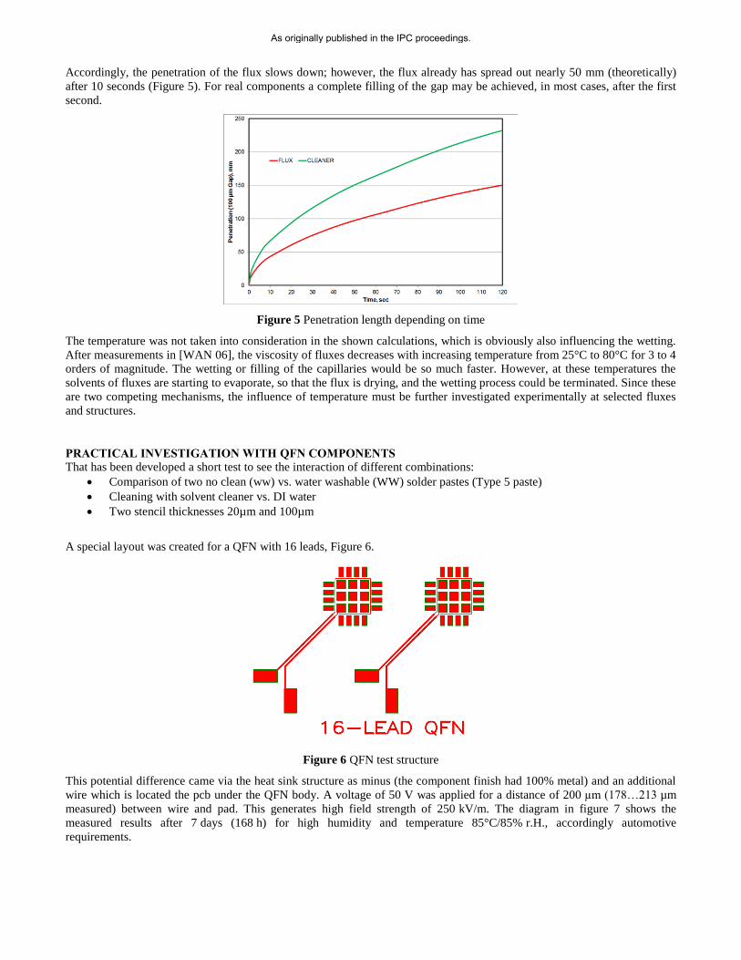
Accordingly, the penetration of the flux slows down; however, the flux already has spread out nearly 50 mm (theoretically)
after 10 seconds (Figure 5). For real components a complete filling of the gap may be achieved, in most cases, after the first
second.
Figure 5 Penetration length depending on time
The temperature was not taken into consideration in the shown calculations, which is obviously also influencing the wetting.
After measurements in [WAN 06], the viscosity of fluxes decreases with increasing temperature from 25°C to 80°C for 3 to 4
orders of magnitude. The wetting or filling of the capillaries would be so much faster. However, at these temperatures the
solvents of fluxes are starting to evaporate, so that the flux is drying, and the wetting process could be terminated. Since these
are two competing mechanisms, the influence of temperature must be further investigated experimentally at selected fluxes
and structures.
PRACTICAL INVESTIGATION WITH QFN COMPONENTS
That has been developed a short test to see the interaction of different combinations:
Comparison of two no clean (ww) vs. water washable (WW) solder pastes (Type 5 paste)
Cleaning with solvent cleaner vs. DI water
Two stencil thicknesses 20µm and 100µm
A special layout was created for a QFN with 16 leads, Figure 6.
Figure 6 QFN test structure
This potential difference came via the heat sink structure as minus (the component finish had 100% metal) and an additional
wire which is located the pcb under the QFN body. A voltage of 50 V was applied for a distance of 200 µm (178…213 µm
measured) between wire and pad. This generates high field strength of 250 kV/m. The diagram in figure 7 shows the
measured results after 7 days (168 h) for high humidity and temperature 85°C/85% r.H., accordingly automotive
requirements.
As originally published in the IPC proceedings.
Page 5
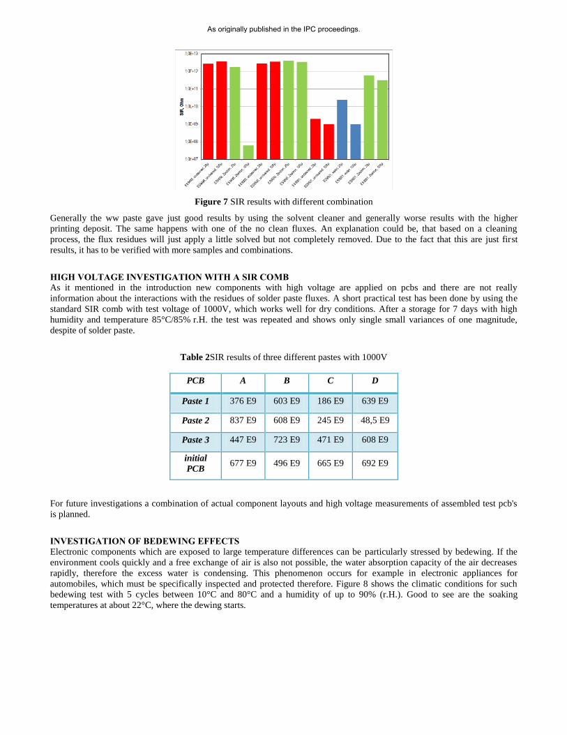
Figure 7 SIR results with different combination
Generally the ww paste gave just good results by using the solvent cleaner and generally worse results with the higher
printing deposit. The same happens with one of the no clean fluxes. An explanation could be, that based on a cleaning
process, the flux residues will just apply a little solved but not completely removed. Due to the fact that this are just first
results, it has to be verified with more samples and combinations.
HIGH VOLTAGE INVESTIGATION WITH A SIR COMB
As it mentioned in the introduction new components with high voltage are applied on pcbs and there are not really
information about the interactions with the residues of solder paste fluxes. A short practical test has been done by using the
standard SIR comb with test voltage of 1000V, which works well for dry conditions. After a storage for 7 days with high
humidity and temperature 85°C/85% r.H. the test was repeated and shows only single small variances of one magnitude,
despite of solder paste.
Table 2SIR results of three different pastes with 1000V
For future investigations a combination of actual component layouts and high voltage measurements of assembled test pcb's
is planned.
INVESTIGATION OF BEDEWING EFFECTS
Electronic components which are exposed to large temperature differences can be particularly stressed by bedewing. If the
environment cools quickly and a free exchange of air is also not possible, the water absorption capacity of the air decreases
rapidly, therefore the excess water is condensing. This phenomenon occurs for example in electronic appliances for
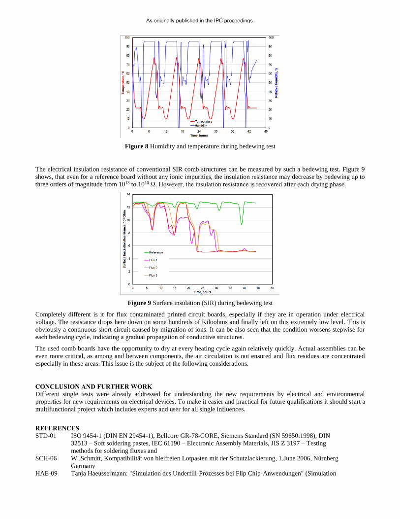
automobiles, which must be specifically inspected and protected therefore. Figure 8 shows the climatic conditions for such
bedewing test with 5 cycles between 10°C and 80°C and a humidity of up to 90% (r.H.). Good to see are the soaking
temperatures at about 22°C, where the dewing starts.
PCB A B C D
Paste 1 376 E9 603 E9 186 E9 639 E9
Paste 2 837 E9 608 E9 245 E9 48,5 E9
Paste 3 447 E9 723 E9 471 E9 608 E9
initial
PCB 677 E9 496 E9 665 E9 692 E9
As originally published in the IPC proceedings.
Page 6
Figure 8 Humidity and temperature during bedewing test
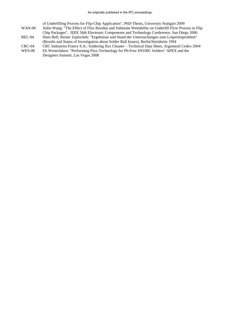
The electrical insulation resistance of conventional SIR comb structures can be measured by such a bedewing test. Figure 9
shows, that even for a reference board without any ionic impurities, the insulation resistance may decrease by bedewing up to
three orders of magnitude from 1013 to 1010 Ω. However, the insulation resistance is recovered after each drying phase.
Figure 9 Surface insulation (SIR) during bedewing test
Completely different is it for flux contaminated printed circuit boards, especially if they are in operation under electrical
voltage. The resistance drops here down on some hundreds of Kiloohms and finally left on this extremely low level. This is
obviously a continuous short circuit caused by migration of ions. It can be also seen that the condition worsens stepwise for
each bedewing cycle, indicating a gradual propagation of conductive structures.
The used comb boards have the opportunity to dry at every heating cycle again relatively quickly. Actual assemblies can be
even more critical, as among and between components, the air circulation is not ensured and flux residues are concentrated
especially in these areas. This issue is the subject of the following considerations.
CONCLUSION AND FURTHER WORK
Different single tests were already addressed for understanding the new requirements by electrical and environmental
properties for new requirements on electrical devices. To make it easier and practical for future qualifications it should start a
multifunctional project which includes experts and user for all single influences.
REFERENCES
STD-01 ISO 9454-1 (DIN EN 29454-1), Bellcore GR-78-CORE, Siemens Standard (SN 59650:1998), DIN
32513 – Soft soldering pastes, IEC 61190 – Electronic Assembly Materials, JIS Z 3197 – Testing
methods for soldering fluxes and
SCH-06 W. Schmitt, Kompatibilität von bleifreien Lotpasten mit der Schutzlackierung, 1.June 2006, Nürnberg
Germany
HAE-09 Tanja Haeussermann: "Simulation des Underfill-Prozesses bei Flip Chip-Anwendungen" (Simulation
As originally published in the IPC proceedings.
Page 7
of Underfilling Process for Flip-Chip Application", PhD-Thesis, University Stuttgart 2009
WAN-06 Jinlin Wang: "The Effect of Flux Residue and Substrate Wettability on Underfill Flow Process in Flip
Chip Packages", IEEE 56th Electronic Components and Technology Conference, San Diego 2006
BEL-94 Hans Bell; Reiner Zajitschek: "Ergebnisse und Stand der Untersuchungen zum Lotperlenproblem"
(Results and Status of Investigation about Solder Ball Issues), Berlin/Steinheim 1994
CRC-04 CRC Industries France S.A.: Soldering flux Cleaner – Technical Data Sheet, Argenteuil Cedex 2004
WES-08 Eli Westerlaken: "Performing Flux-Technology for Pb-Free SN100C Solders" APEX and the
Designers Summit, Las Vegas 2008
As originally published in the IPC proceedings.