iCC 2013 CAN in Automation 04-1 Next Generation CAN FD Controller Core Daniel Leu, Inicore The new CAN FD specification offers several enhancements over the current ISO 11898-1 standard such as an eightfold increase in the data field length and enhanced data throughput. In order to provide high efficiency of the software, the CAN controller’s host interface and message handling need to be streamlined and optimized. This paper discusses the implementation and verification of a new FIFO-based CAN FD core with an application programming interface that minimizes processor read and write cycles and has dedicated sideband signals to support DMA-based message transfers. The core contains supportive debug logic to assist the system in analyzing and optimizing CAN traffic, something especially important when using higher data rates. Verification testbench and lab setup are presented as well. In modern system-on-chip (SOC) designs, the CAN interface is located together with other low-speed peripherals. Although the data throughput of the new CAN FD is significantly higher than that of regular CAN, it is still marginal compared to Gigabit Ethernet, USB 3 or other high performance interfaces. Figure 1 shows a typical architecture of a modern SOC with several local buses that are interconnected with bus bridges. A CAN interface can placed at many different locations. Figure 1: System-on-chip architecture – CAN 1 is connected to the main system bus: it is very unlikely to have the CAN peripheral directly connected to the system bus due to its low-performance characteristics. – CAN 2 is connected to the preliminary peripheral bus: this is a very likely setup for regular peripheral devices. – CAN 3 is connected to the secondary peripheral bus: in more complex systems with additional high- performance buses, the CAN peripheral might move even further away from the processor. – CAN 4 as a standalone CAN controller connected to the SOC via an external bus interface (EBI). We looked at some timing data from FPGA SOC devices. Table 1 shows the maximum frequency the processor and the different buses run at. For this analysis, the absolute value of the bus frequency is not important. The interesting factor is the ratio of the processor to the peripheral bus frequency. In most devices, this ratio can be changed to conserve power if a sub-bus doesn’t need to run at the maximal frequency. SOC Architecture Processor Processor Cache System Bus Memory EBI CAN 4 Peripheal Bridge Peripheral Bus 1 CAN 1 CAN 2 Bus Bridge Performance Bus Peripheal Bridge Peripheral Bus 2 CAN 3 ...
Transcript
iCC 2013 CAN in Automation
04-1
Next Generation CAN FD Controller Core
Daniel Leu, Inicore The new CAN FD specification offers several enhancements over the current ISO 11898-1 standard such as an eightfold increase in the data field length and enhanced data throughput. In order to provide high efficiency of the software, the CAN controller’s host interface and message handling need to be streamlined and optimized. This paper discusses the implementation and verification of a new FIFO-based CAN FD core with an application programming interface that minimizes processor read and write cycles and has dedicated sideband signals to support DMA-based message transfers. The core contains supportive debug logic to assist the system in analyzing and optimizing CAN traffic, something especially important when using higher data rates. Verification testbench and lab setup are presented as well. In modern system-on-chip (SOC) designs, the CAN interface is located together with other low-speed peripherals. Although the data throughput of the new CAN FD is significantly higher than that of regular CAN, it is still marginal compared to Gigabit Ethernet, USB 3 or other high performance interfaces. Figure 1 shows a typical architecture of a modern SOC with several local buses that are interconnected with bus bridges. A CAN interface can placed at many different locations.
Figure 1: System-on-chip architecture
– CAN 1 is connected to the main system bus: it is very unlikely to have the CAN peripheral directly connected to the system bus due to its low-performance characteristics.
– CAN 2 is connected to the preliminary peripheral bus: this is a very likely setup for regular peripheral devices.
– CAN 3 is connected to the secondary peripheral bus: in more complex systems with additional high-performance buses, the CAN peripheral might move even further away from the processor.
– CAN 4 as a standalone CAN controller connected to the SOC via an external bus interface (EBI).
We looked at some timing data from FPGA SOC devices. Table 1 shows the maximum frequency the processor and the different buses run at. For this analysis, the absolute value of the bus frequency is not important. The interesting factor is the ratio of the processor to the peripheral bus frequency. In most devices, this ratio can be changed to conserve power if a sub-bus doesn’t need to run at the maximal frequency.
SOC Architecture
Processor Processor
Cache
System Bus
Memory EBI
CAN 4
Peripheal Bridge
Peripheral Bus 1
CAN 1
CAN 2
Bus Bridge
Performance Bus
Peripheal Bridge
Peripheral Bus 2
CAN 3
...
iCC 2013 CAN in Automation
04-2
Table 1: Bus performance in MHz
Device Proces-sor
System bus
Peripheral bus
Altera Aria V 800 400 200 Microsemi SmartFusion 100 100 50
Microsemi SmartFusion 2 166 166 166
Xilinx Zinq1 600 300 150 Xilinx Zinq2 800 266 133
The location of a peripheral device in a SOC has a significant performance impact. The further away the peripheral device is from the processor, the longer it takes for the data to travel. There are different sources that impact this delay: – A system bus usually runs at a lower
frequency than the processor. – Every time data crosses from one bus
to another, a delay of one or more clock cycles is introduced.
– Accessing a new bus might be delayed because of an already ongoing data transfer.
– Sub-buses tend to run at a lower frequency than main buses.
– Accessing external devices is always slow.
All these delays add up and slow down a data read or write cycle to a peripheral device. But there are ways to address this: 1) Modern system buses provide the option to transfer data in blocks. This doesn’t change any of the delays seen for a single transfer, but each additional data word just takes one or two extra peripheral clock cycles. 2) Instead of having the processor fetching the data, an external direct memory access (DMA) controller can transfer it in the background while the processor continues its normal operation. To summarize, it is important to have the following goals – among others, in mind when designing a peripheral device for a modern SOC: – Limit the number of access cycles 1 Using 4:2:1 clock ratio selection 2 Using 6:2:1 clock ratio selection
– Support block transfers – Support data transfers without or only
with limited processor involvement
Features
As a lucky coincidence, CAN FD came along exactly when we started planning our next generation CAN controller core. With the higher data throughput, this nicely fit into the features we had already laid out: General architecture: – FIFO based – Separate clock domains for CAN and
system logic – Optimized API – Support for external DMA controller – Error capture feature to support bus
debugging – Designed for FPGA and ASIC targets
Receive Buffer improvements: – Up to two receive FIFOs – Up to 32 enhanced message filters with
mask and range match mode; covering ID, new CAN FD control flags and two most significant data bytes
– Programmable FIFO length and message length
– 32-bit timestamp Transmit Buffer improvements: – One transmit FIFO that preserves
message order (no priority inversion) – One transmit queue where the highest
priority message is sent first. – Programmable FIFO and queue length
and message length – Support for message tag We then added the support for the CAN FD and mixing and matching CAN 2.0 A/B and CAN FD messages.
Ease of use
Although CAN FD brings new features and complexities to a CAN controller, it does not mean that it needs to be more difficult to use. The API of our CAN FD controller
iCC 2013 CAN in Automation
04-3
core, CANmodule, was designed with ease-of-use in mind: – Consistent buffer size: All message
objects of a given message buffer (eg. RxFIFO0) have the same size.
– Identical layout for receive and transmit buffer
– Configurable number of message objects per buffer
– Targets 32-bit bus systems – Designed to minimize access cycles
CANmodule overview
As stated earlier, our next generation CAN controller uses FIFOs as message buffers. A common core external memory is used for storage.
Figure 2: CANmodule Block diagram This way, one can configure the core to optimally use the available resources and match the application requirements. – The CAN Engine handles the low-level
CAN bus traffic. – The Memory Arbiter manages access
requests to the common memory. – The Receive Handler performs the
message filtering and contains the receive FIFO logic.
– The Transmit Handler contains the transmit FIFO and Queue and the message arbiter to select the highest priority message.
– The Bus Interface has the logic to connect to the host bus as well as all configuration registers, interrupt and debug logic.
– The block DMA Support contains the dedicated logic for DMA support and the necessary DMA sideband signals.
DMA support
Using an on-chip DMA controller greatly reduces the processor overhead related to moving data. The DMA controller autonomously transfers data between the peripheral and system memory. The processor only gets interrupted once the programmed data transfer is complete.
Figure 3: DMA data sequence (receive) Once the DMA controller and the CANmodule are programmed for DMA transfers, data is transferred between the peripheral and the system memory:
1) The CANmodule asserts dma_req to indicate that enough data is available for a transfer.
2) The DMA controller fetches the data from the requesting device
3) Then stores it in the destination memory.
4) Once the programmed number of words are transferred, the dma_irq is asserted and the processor receives this interrupt.
The CANmodule provides all necessary sideband signals to support both simple DMA controllers, that only have a dma_req signal, and complex DMA controllers that have a more sophisticated interface.
CANmodule
CAN Engine
can_tx
can_rx
ReceiveHandler
TransmitHandler
Memory Arbiter
SRAM
BusInterface
DMASupport
ARM Cortex-M3 INTC
Bus Bridge
Peripheral Bus
System Bus
SRAM
can_txcan_rx
DMA
CANmodule
dma_req
dma_irq
12
3
4
iCC 2013 CAN in Automation
04-4
If DMA transfers are not used, dma_req can be repurposed as a dedicated interrupt signal to indicate that receive data is available or that the transmit FIFO can accept more data. In order to support DMA operation, the CANmodule contains an auto-acknowledge / auto-transmit feature. If enabled, this works like this: – On the Receive buffer:
Once an entire message is read, the message acknowledge flag is automatically asserted. There is no need to set this flag by an additional write operation.
– On the Transmit buffer: Once the entire message has been written, the message transmit request flag is automatically set. There is no need for an additional write or read/modify/write operation.
This auto-acknowledge / auto-transmit feature can also be used independently of the DMA operation.
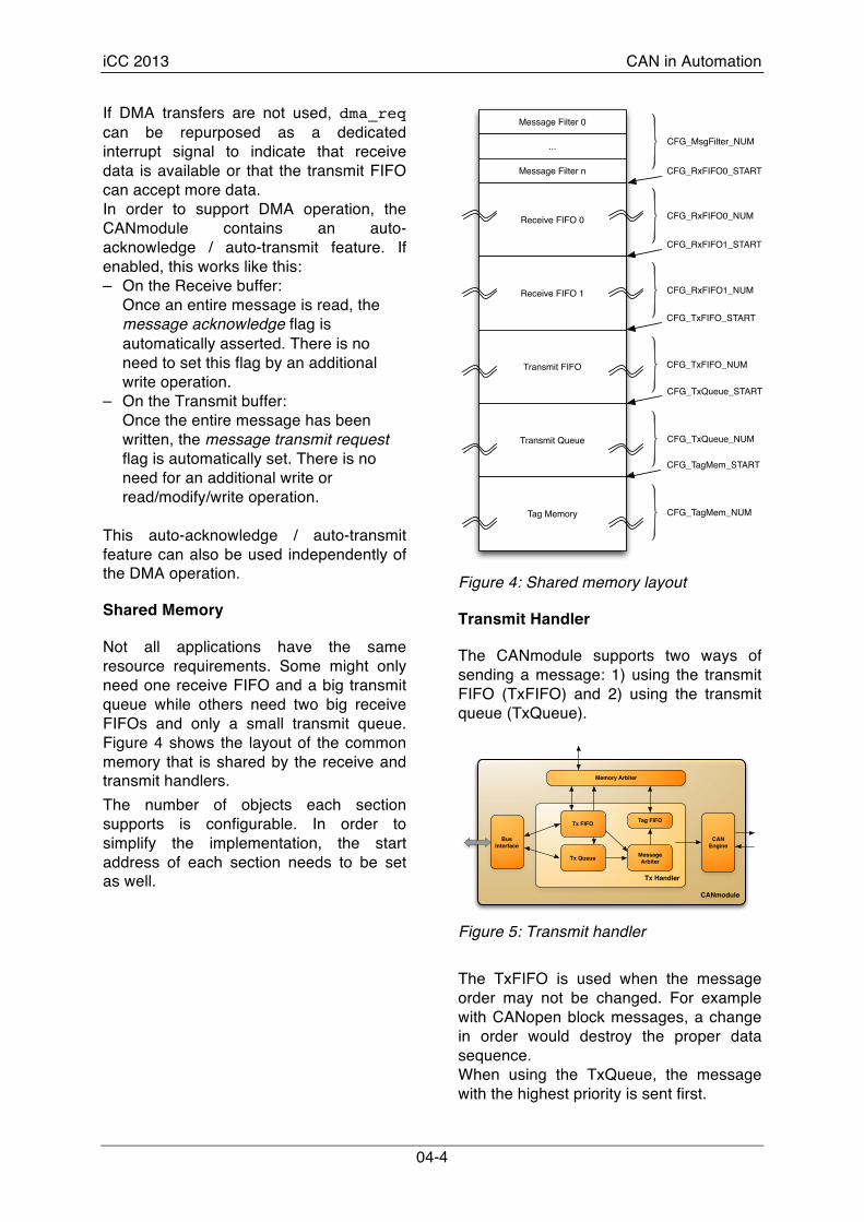
Shared Memory
Not all applications have the same resource requirements. Some might only need one receive FIFO and a big transmit queue while others need two big receive FIFOs and only a small transmit queue. Figure 4 shows the layout of the common memory that is shared by the receive and transmit handlers. The number of objects each section supports is configurable. In order to simplify the implementation, the start address of each section needs to be set as well.
Figure 4: Shared memory layout
Transmit Handler
The CANmodule supports two ways of sending a message: 1) using the transmit FIFO (TxFIFO) and 2) using the transmit queue (TxQueue).
Figure 5: Transmit handler The TxFIFO is used when the message order may not be changed. For example with CANopen block messages, a change in order would destroy the proper data sequence. When using the TxQueue, the message with the highest priority is sent first.
Message Filter 0
...
Message Filter n
Receive FIFO 0
Receive FIFO 1
Transmit FIFO
Transmit Queue
CFG_RxFIFO0_START
CFG_RxFIFO1_START
CFG_TxFIFO_START
CFG_TxQueue_START
CFG_RxFIFO0_NUM
CFG_RxFIFO1_NUM
CFG_TxFIFO_NUM
CFG_TxQueue_NUM
CFG_MsgFilter_NUM
Tag Memory CFG_TagMem_NUM
CFG_TagMem_START
CANmodule
Tx Handler
Memory Arbiter
Tx Queue MessageArbiter
BusInterface
CAN Engine
Tag FIFOTx FIFO
iCC 2013 CAN in Automation
04-5
Whenever a message is sent, aborted or a single-shot transmission error is detected, an entry is added to the Tag FIFO. An entry consists of the result code, message identifier, tag field and the timestamp.
Receive handler
The receive handler contains two receive FIFOs (RxFIFO 0/1) that can be individually configured.
Figure 6: Receive handler Whenever a new message arrives, the Receive Handler checks it against all message filter settings. If a match is found, the message is stored in the specified RxFIFO. Whenever the start-of-frame (SOF) field of a new message is detected, the actual timestamp is saved and added to the message when it is stored in the RxFIFO. There are applications where it is very important to synchronize all nodes with a special sync message. The CANmodule contains a hardware trigger output (hw_trigger) that is asserted whenever a match on message filter 0 is detected. This output can be used as a dedicated interrupt source or it can directly feed user logic that synchronizes a hardware based timer. Design Verification Prior to using the core inside an FPGA in the lab, we verified it through simulation. We developed two different testbenches. A CAN conformance testbench to verify the low-level CAN protocol on a time-quanta basis, and a system-level testbench to verify the host bus interface and all the message handling.
CAN conformance testbench The testbench shown in Figure 7 is based on the test procedures defined in ISO 16845 and enhanced for CAN FD.
Figure 7: CAN conformance testbench The meanings of the different blocks are: – DUT: Device Under Test (CANmodule) – DUT Handler: this is a simple state-
machine that decodes and executes commands received via the CAN bus.
– CAN Transceiver Functional Model: this models CAN bus transceiver with programmable transmit and receive delays
– CAN Logger: this module logs CAN activity and reports any errors detected.
– CAN BFM: the CAN Bus Functional Model generates the bus traffic based on command received from the Stimuli Generator
– Stimuli Generator: these modules implement the test procedures and execute them. Results are checked against the expected value and success and errors are reported.
System-level Testbench The testbench shown in Figure 8 is used to verify the entire message handling and processor interface of the CANmodule. The block diagram looks very similar to that of the conformance testbench and many components are shared. The main difference is that we use a bus functional model for the host interface (APB or AXI BFM), which is controlled by the stimuli generator block.
CANmodule
Rx Handler
Memory Arbiter
Rx FIFO 1
MessageFilter
BusInterface
CAN Engine
Rx FIFO 0
hw_trigger Stimuli Generator
DUTCAN
TransceiverFM
CANbus
CANLogger
CANBFM
DUT Handler
Stimuli GeneratorStimuli Generator
iCC 2013 CAN in Automation
04-6
Figure 8: System-level testbench Several Stimuli Generators are used to exercise the DUT to cover all regular and error scenarios, so that everything would be verified before programming an FPGA going to the lab for hardware verification.
FPGA Design
SOC FPGAs nowadays contain entire microcontroller subsystems with all standard features of a standalone processor combined with a traditional FPGA fabric. They serve as a very flexible platform for custom microprocessor-based integrations. We used Microsemi’s SmartFusion FPGA as our test vehicle to verify proper operation of the CANmodule in our lab. An APB3 bus master is exposed to the FPGA fabric that connected to our local APB3 bus and the CANmodule core.
Figure 9: FPGA block diagram We have two different versions of this FPGA, one with one CAN channel and a second with two CAN channels.
Hardware Setup
To show and test proper operation of the CANmodule with the new CAN FD protocol, we setup a simple 5-node network in our lab. It consist of following components: – Vector VN1630: Dual channel CAN
network interface using the Bosch M-CAN module implemented in a FPGA. These two nodes are the reference in our system.
– FPGA board 2 (bottom right): Single channel CANmodule implementation as shown in Figure 9.
Figure 10: Lab setup of CAN network
In our test setup, we use one channel of the VN1630 as the protocol logger and the other as a test generator. On the two FPGA boards, we have test software running that generates CAN FD frames with different data lengths, varying ID and data content.
Outlook
The presented implementation uses a standard AMBA APB3 bus interface. APB3 is a slow peripheral bus with a data and an address phase. A future version of the core will use a higher performance AXI interface that supports burst mode. Once CAN FD is standardized and the ISO 16845 CAN conformance test plan is updated, we will submit the CANmodule to C&S for conformance testing.
Stimuli Generator
DUTCAN
TransceiverFM
CANbus
CANLogger
CANBFM
APB or AXIBFM
Stimuli GeneratorStimuli Generator
FPGA Fabric
Microcontroller Subsystem
ARM Cortex-M3 ENVM
UART
TIMER
INTC
CANmodule
APB Bridge
APB Bus
AHB Bus
APB Bridge SRAM
APB Bus
can_txcan_rx
can_int_req
iCC 2013 CAN in Automation
04-7
Daniel Leu Inicore Inc. 5600 Mowry School Road, Suite 180 US-94560 Newark, CA Tel.: +1 510 445 1529 Fax: +1 510 656 0995 [email protected] www.inicore.com References [1] Bosch, CAN with Flexible Data-Rate,
White Paper, Version 1.1 [2] Inicore CANmodule-4 Datasheet,
Preliminary Version [3] Xilinx Zynq-7000 AP SoC Technical