Next generation ferroelectric materials for semiconductor process integration and their applications Cite as: J. Appl. Phys. 129, 100901 (2021); doi: 10.1063/5.0037617 View Online Export Citation CrossMark Submitted: 14 November 2020 · Accepted: 10 February 2021 · Published Online: 11 March 2021 T. Mikolajick, 1,2,a) S. Slesazeck, 1 H. Mulaosmanovic, 1 M. H. Park, 3 S. Fichtner, 4 P. D. Lomenzo, 1 M. Hoffmann, 1 and U. Schroeder 1 AFFILIATIONS 1 NaMLab gGmbH, Noethnitzer Str. 64, D-01187 Dresden, Germany 2 Institute of Semiconductors and Microsystems (IHM), TU Dresden, D-01062 Dresden, Germany 3 School of Materials Science and Engineering, Pusan National University, 2 Busandaehak-ro 63beon-gil, Geumjeong-gu, Busan 46241, Republic of Korea 4 Materials and Processes for Micro/Nanosystem Technologies, Universityof Kiel, Institute for Material Science, Kaiserstr. 2, 24143 Kiel, Germany a) Author to whom correspondence should be addressed: [email protected]ABSTRACT Ferroelectrics are a class of materials that possess a variety of interactions between electrical, mechanical, and thermal properties that have enabled a wealth of functionalities. To realize integrated systems, the integration of these functionalities into semiconductor processes is nec- essary. To this end, the complexityof well-known ferroelectric materials, e.g., the perovskite class, causes severe issues that limit its applica- tions in integrated systems. The discovery of ferroelectricity in hafnium oxide-based materials brought a renewed interest into this field during the last decade. Very recently, ferroelectricity was also verified in aluminum scandium nitride extending the potential of seeing a wealth of ferroelectric functions in integrated electronics in the future. This paper discusses the prospects of both material systems in various applications. Published under license by AIP Publishing. https://doi.org/10.1063/5.0037617 I. INTRODUCTION A ferroelectric (FE) material has two stable polarization states that can be switched from one state into another state by applying an electric field. 1,2 To qualify as a ferroelectric, a material, therefore, needs to have a stable polarization at zero applied field referred to as remanent polarization. Since such ferroelectric polarization is temperature dependent, all ferroelectric materials are also pyroelec- tric. Moreover, the switching dipoles give rise to a field dependent volume change of the material and, therefore, all ferroelectrics and pyroelectrics are piezoelectric. 3 As a result, ferroelectric materials have a plurality of interesting properties that show a dependence on the applied electric field, temperature, strain, and other parameters. Therefore, they are useful in a wealth of applications including capacitors, memory cells, sensors, actuators, energy storage, and more. 4,5 When it comes to the usage of ferroelectrics in integrated circuits, the defining property of the ferroelectric, namely, switch- able polarization, is the most important property since it can be used for information storage. 5,211,214,215 Here, the field driven switching mechanism, together with the fact that the polarization state will be retained for long times, makes the material an ideal choice to realize nonvolatile memories with low write power. To realize ferroelectricity in a crystal, the crystal necessarily needs to have a non-centrosymmetric structure together with the ability to switch the position of one or several ions in the lattice between two stable states. This makes ferroelectricity a rare material property that historically could only be observed in quite complex crystal structures involving three or more elements like perovskites. Such materials are difficult to integrate into a semiconductor man- ufacturing process that has strong requirements with respect to thermal budget, exposure to forming gas anneals, and tight control Journal of Applied Physics PERSPECTIVE scitation.org/journal/jap J. Appl. Phys. 129, 100901 (2021); doi: 10.1063/5.0037617 129, 100901-1 Published under license by AIP Publishing.
Transcript
Next generation ferroelectric materialsfor semiconductor process integrationand their applications
Cite as: J. Appl. Phys. 129, 100901 (2021); doi: 10.1063/5.0037617
View Online Export Citation CrossMarkSubmitted: 14 November 2020 · Accepted: 10 February 2021 ·Published Online: 11 March 2021
T. Mikolajick,1,2,a) S. Slesazeck,1 H. Mulaosmanovic,1 M. H. Park,3 S. Fichtner,4 P. D. Lomenzo,1
M. Hoffmann,1 and U. Schroeder1
AFFILIATIONS
1NaMLab gGmbH, Noethnitzer Str. 64, D-01187 Dresden, Germany2Institute of Semiconductors and Microsystems (IHM), TU Dresden, D-01062 Dresden, Germany3School of Materials Science and Engineering, Pusan National University, 2 Busandaehak-ro 63beon-gil, Geumjeong-gu,
Busan 46241, Republic of Korea4Materials and Processes for Micro/Nanosystem Technologies, University of Kiel, Institute for Material Science, Kaiserstr. 2,
24143 Kiel, Germany
a)Author to whom correspondence should be addressed: [email protected]
ABSTRACT
Ferroelectrics are a class of materials that possess a variety of interactions between electrical, mechanical, and thermal properties that haveenabled a wealth of functionalities. To realize integrated systems, the integration of these functionalities into semiconductor processes is nec-essary. To this end, the complexity of well-known ferroelectric materials, e.g., the perovskite class, causes severe issues that limit its applica-tions in integrated systems. The discovery of ferroelectricity in hafnium oxide-based materials brought a renewed interest into this fieldduring the last decade. Very recently, ferroelectricity was also verified in aluminum scandium nitride extending the potential of seeing awealth of ferroelectric functions in integrated electronics in the future. This paper discusses the prospects of both material systems invarious applications.
Published under license by AIP Publishing. https://doi.org/10.1063/5.0037617
I. INTRODUCTION
A ferroelectric (FE) material has two stable polarization statesthat can be switched from one state into another state by applyingan electric field.1,2 To qualify as a ferroelectric, a material, therefore,needs to have a stable polarization at zero applied field referred toas remanent polarization. Since such ferroelectric polarization istemperature dependent, all ferroelectric materials are also pyroelec-tric. Moreover, the switching dipoles give rise to a field dependentvolume change of the material and, therefore, all ferroelectrics andpyroelectrics are piezoelectric.3 As a result, ferroelectric materialshave a plurality of interesting properties that show a dependence onthe applied electric field, temperature, strain, and other parameters.Therefore, they are useful in a wealth of applications includingcapacitors, memory cells, sensors, actuators, energy storage, andmore.4,5 When it comes to the usage of ferroelectrics in integrated
circuits, the defining property of the ferroelectric, namely, switch-able polarization, is the most important property since it can beused for information storage.5,211,214,215 Here, the field drivenswitching mechanism, together with the fact that the polarizationstate will be retained for long times, makes the material an idealchoice to realize nonvolatile memories with low write power.
To realize ferroelectricity in a crystal, the crystal necessarilyneeds to have a non-centrosymmetric structure together with theability to switch the position of one or several ions in the latticebetween two stable states. This makes ferroelectricity a rare materialproperty that historically could only be observed in quite complexcrystal structures involving three or more elements like perovskites.Such materials are difficult to integrate into a semiconductor man-ufacturing process that has strong requirements with respect tothermal budget, exposure to forming gas anneals, and tight control
of the elements used within the production line. As a result, ferro-electrics integrated into semiconductor processes had limitedmarket success so far. In 2011, it was reported for the first timethat in doped hafnium oxide (HfO2), ferroelectricity could beachieved.6 This discovery changed the prospects of integratingferroelectrics into complementary metal–oxide–semiconductor(CMOS) processes since hafnium oxide is a standard material usedeven in the front end of CMOS processes since 2007.7 Morerecently, the piezoelectricity available in AlN could be turned into aswitchable ferroelectricity in AlScN.8 This material would be ideallysuited for the integration with GaN technology, but it also promisesoptions for CMOS back end of line integration. Finally, the effortsof making 2D materials usable in electron devices also yielded veryinteresting ferroelectrics.9,10 The following article will deal withhafnium oxide-based ferroelectrics as well as AlScN based ferro-electrics since these materials are closest to the real application and,therefore, are very promising to enter commercial semiconductorprocesses in the next five to ten years.
II. HISTORY OF FERROELECTRIC MATERIALSAND DEVICES
Recently, the 100th anniversary for the discovery of ferroelec-tricity in Rochelle salts was celebrated.11,12 While the interestingproperties immediately spurred further research that brought upadditional systems like potassium-dihydrogen phosphate, orKDP,13 these material systems were too sensitive and water-solublefor practical applications. The discovery of ferroelectricity inbarium titanate BaTiO3 (BTO)
14–16 paved the way for applicationsin sensors and capacitors. Already in the 1950s, Buck proposed theusage of ferroelectrics for memory applications,17 and this proposalinspired additional research activities.18,19 These did not result inproducts appearing on the market, and integrated circuit technol-ogy, as we know it today, was not yet available in those days.Nevertheless, those early devices that contained hundreds ofmemory cells on a single BTO substrate can be considered the firstdemonstration of an integrated memory devices.
On the material side, the lead-zirconium titanate Pb[ZrxTi1−x]O3 (PZT) system20,21 brought another big step in the 1950s. LikeBTO, PZT has a perovskite structure. However, the mixture of Zrand Ti based oxides brings additional flexibility and particularly atthe morphotropic phase boundary between the tetragonal andrhombohedral ferroelectric phases possesses excellent ferroelectricproperties. In the second half of the 1950s, the concept of a ferro-electric field-effect transistor (FeFET) was proposed for the firsttime.22 But it took a very long time until such a device wouldproduce useful characteristics including nonvolatile retention.23
While basic research on those and other ferroelectric memoriescontinued, the development of integrated circuit processes finallyenabled the realization of a ferroelectric memory that could fulfillall of the requirements to be commercialized in the early 1990s.24
Besides using PZT instead of BTO, the main difference comparedto the early attempts from the 1950s was that a select transistor wasadded to the memory cell to result in a similar cell structure that isknown from dynamic random access memories (DRAMs). Theselect transistor made it possible to eliminate problems from halfselects of other bitlines and wordlines. Nevertheless, PZT suffered
from fatigue, which is the degradation of the switchable polariza-tion with increasing read and write cycles.
Layered perovskites that have oxide interlayers between perov-skite layers like strontium bismuth tantalate Sr2Bi2TaO9 (SBT) wereintroduced in the 1990s as a solution to fatigue.25 However, theeven more complex crystal structure made the integration of thelayered perovskites into semiconductor fabrication processes evenmore troublesome than it was for PZT. Therefore, the commercialsuccess was limited since around the same time, fatigue in PZT wasfound to be greatly reduced by using oxide electrodes like IrO2,RuO2, and related materials.26 Even after solving the fatigue issuein PZT, the required crystallization, problematic inclusion of lead,and the weakly bound oxygen make perovskites and layeredperovskites still very difficult to integrate into CMOS processes.27
As a result, the most advanced technology is in the 130 nm node28
and the three-dimensional integration issue could not be solved upto now.29 In the mid-2000s, the first demonstration of the nonvola-tile operation of a FeFET based on SBT was finally achieved.30 Inthe same time period, a concept based on the switchable tunnelingcurrent through a very thin ferroelectric that was first proposed byEsaki et al. back in 197131 was finally realized32 adding ferroelectrictunnel junctions (FTJs) as a third option to the portfolio of ferro-electric memory devices. However, these devices need high qualityepitaxial ferroelectrics.33 This approach is extremely unlikely to beintegrated into a CMOS process. With the known processes for epi-taxial growth of such layers and the required lattice matched elec-trodes, epitaxial growth directly on a CMOS compatible substratecannot be achieved. An interesting alternative approach for inte-grating such complex oxide films is to grow the epitaxial films on adifferent substrate and transfer them to the CMOS wafer,34,35 butthis technique is still in the basic research phase and many years ofresearch will be required to see if this could be a viable path towardCMOS integration. The field, therefore, seems to be stuck in a sit-uation where extremely promising memory properties were demon-strated for three fundamentally different device types, but theintegration into state-of-the-art CMOS processes was hindered bythe integration issues due to the rather complex materials.
The first report of ferroelectricity in silicon doped hafniumoxide in 20116 changed that picture and immediately resultedin the realization of a FeFET with very promising properties.36
The stabilization of ferroelectricity by several other dopants37 andthe demonstration of three-dimensional structures for capacitorbased ferroelectric random access memory (FeRAM),38 as well asthe demonstration of integrated FeRAM devices39 and FTJs,40,41
show that this material system immediately brought new life intothe field of ferroelectric devices. Besides realizing memories, ferro-electric hafnium oxide is the only material system that could possi-bly be used when realizing a new type of steep slope deviceproposed in 2008 under the term negative capacitance field-effecttransistor (NCFET)42 that is still controversially discussed in thecommunity43 and requires much more basic understanding toverify its potentials and limitations.44 Finally, in 2019, anotherinteresting new material AlScN was added to the list of new ferro-electrics.8 While in hafnium oxide-based ferroelectrics, a phase thatis normally not stable in bulk materials is stabilized in thin films,in the AlScN system, a well-known piezoelectric material was madeferroelectric. Again, a ferroelectric material that is much more
compatible to semiconductor processing is added. The timeline offerroelectric materials and ferroelectruc semiconductor devices isillustrated in Fig. 1.
III. FERROELECTRIC MATERIALS
A. Traditional ferroelectric materials
Ferroelectricity can be shown in various types of materialswith non-centrosymmetric crystalline structures, and they can becategorized into various groups according to their mechanismbehind ferroelectricity. In this section, however, only those materi-als, which have been seriously considered for being utilized insemiconductor industry, are focused on. The first and second
discovered ferroelectric materials were Rochelle salt11 andKH2PO4
13 in 1920 and 1935, respectively. After the discovery offerroelectricity in perovskite structure BaTiO3, the ferroelectricmaterials attracted significant interest from the 1940s on Ref. 16.Since then, the perovskite structure ferroelectrics have been thelargest group among various material groups to date.
Figure 2 and Table I summarize the crystalline structures andmaterial properties of several relevant conventional ferroelectrics:Pb(Zr,Ti)O3 (PZT), SrBi2Ta2O9 (SBT), and BiFeO3 (BFO). PZT isthe most intensively studied ferroelectric material for various appli-cations including FeRAMs, actuators, and sensors based on itsstrong ferroelectricity and piezoelectricity. Its remanent polarization(Pr) is generally 10–40 μC/cm
2 in thin films and can be even higher
FIG. 1. Timeline of ferroelectric materials and ferroelectric semiconductor devices.
FIG. 2. Conventional ferroelectric materials: Pb(Zr,Ti)O3, SrBi2Ta2O9, and BiFeO3.
than 70 μC/cm2, so in FeRAM capacitors of nonvolatile memorycell, a large quantity of charges can be stored. When PZT wasfirst adopted to FeRAMs, the limited number of endurable cycleswith significant fatigue was a critical issue using Pt electrodes,45 soother oxide electrodes such as IrO2 were introduced to achieve anendurance that was sufficient for practical FeRAMs. SBT attractedintensive focus for FeRAM application, since it could exhibitfatigue-free performance on Pt electrodes.25 The remanent polari-zation Pr of SBT thin films is 5–10 μC/cm2, which is smaller com-pared to that of PZT, but it is sufficient to control the Si channelconductivity in FeFETs and for storing charges in FeRAM cells. Asa result, SBT was intensively studied for FeRAMs and FeFETs withhigh reliability despite its complexity in chemical composition andcrystalline structure. BFO is based on a rhombohedral perovskitestructure, and it could exhibit polarization as high as ∼100 μC/cm2.46,47 With such high polarization, BFO has attracted increasinginterest for various applications. However, as insulating ferroelectricceramics for memory technology, BFO has the intrinsically criticalissue of a small bandgap (2.0–2.5 eV). Instead, BFO can exhibit fer-romagnetic properties as well as giant ferroelectric property, whichenables applications based on electro-magnetic coupling even atroom temperature. Moreover, with a bandgap significantly smallerthan those of PZT or SBT, BFO was suggested to be promising forphotovoltaic applications.48
B. Hafnium and zirconium based ferroelectrics
The ferroelectricity in Si-doped HfO2 was first reported in 2011by Böscke and co-workers.36,49 Different from conventional ferroelec-tric materials that suffer from the serious degradation of ferroelectric-ity in ultra-thin films, a robust ferroelectricity with Pr higher than15 μC/cm2 could be achieved with 10 nm film thickness.36 This pio-neering work was followed by numerous reports on ferroelectricity inHfO2 or ZrO2 induced by various dopants and depositiontechniques.50–56 Figure 3(a) shows several polymorphs of HfO2 andZrO2 frequently observed in thin films, and the crystallographic originof the ferroelectricity is the formation of the Pca21 orthorhombicphase, as demonstrated by Sang et al.57 using convergent beam elec-tron beam diffraction. Generally, nanoscale competition between dif-ferent crystalline phases can be observed in doped HfO2 or ZrO2 thinfilms, which is affected by various factors including doping, thickness,impurities, temperature, and even electric field cycling. Such
complicated nanoscale polymorphism can be attributed to the meta-stability of the ferroelectric orthorhombic phase.58–63
Figures 3(b)–3(d) show the effect of doping on x-raydiffraction (XRD) pattern, aspect ratio, and relative phase frac-tion, respectively.64 As can be seen in Fig. 3(b), the dominantcrystalline phase changes from monoclinic to orthorhombic totetragonal/cubic phase with increasing doping concentration, andthere exist a specific doping concentration range dependent ondopant species where strong ferroelectricity with high orthorhom-bic phase fraction can be achieved. The ideal aspect ratios, whichare relative ratios of the largest lattice parameter to the shorterones, expected for the orthorhombic and tetragonal phase are∼1.03–1.04 and 1.01–1.02, respectively.65 Thus, a high aspectratio is one important sign of ferroelectricity in doped HfO2 orZrO2. As reported by Park et al.,65 the Rietveld refinement can beutilized to quantitatively analyze the relative fractions of differentcrystalline phases. Figure 3(d) shows the Rietveld refinementresult of La-doped HfO2 thin films with various doping concen-trations, which is consistent with changes in ferroelectric proper-ties. As shown in Fig. 3(e), the unit cell size of the ferroelectricorthorhombic phase increases with increasing dopant radius.
The film thickness is another factor that critically affects theferroelectricity in doped HfO2 or ZrO2 films. Figure 3(f ) shows thechanges in the Pr value of HfO2 films doped with various dopantsas functions of the film thickness.64 Generally, the orthorhombicphase fraction as well as Pr decrease with increasing film thicknessand, therefore, with decreasing surface-to-volume ratio. As sug-gested by Materlik et al.,58 the polymorphism in fluorite-structureferroelectrics is strongly influenced by a surface energy effect. Theeffect of the thickness on the coercive field (Ec) in fluorite-structureferroelectrics is different from normal ferroelectrics as shown inFig. 3(g).66 It is generally known that Ec of ferroelectrics is propor-tional to d−3/2, but the thickness dependence of polycrystallineHf0.5Zr0.5O2 or epitaxial Y:HfO2 is much weaker than expectationfrom the Kay–Dunn model.67 The authors have shown that smallcrystallites shift independent of their environment and even micro-meter thick films consist of these nanometer sized crystallites,which determine the switching kinetics. A schematic phasediagram for HfO2–ZrO2 solid solution with various doping concen-trations and thicknesses can be seen in Fig. 3(h).68 The monoclinicphase fraction is higher for thicker and Hf-richer films, while thetetragonal phase fraction is higher for thinner and Zr-richer films.
TABLE I. Comparison of ferroelectric materials PZT, SBT, BFO, doped HfO2, and AlxSc1−xN.
FIG. 3. (a) General trend in polymorphism in ferroelectric doped HfO2 thin films. (b) X-ray diffraction patterns of La:HfO2 and Si:HfO2 thin films. The changes in (c) aspectratio/unit cell volume and (d) relative phase fraction in La:HfO2 as functions of La content. (e) The unit cell volume of the ferroelectric orthorhombic phase as a function of ionicradius of dopants. (a) Reproduced with permission from Park et al., J. Mater. Chem. C 5(19), 4677–4690 (2017). Copyright 2017 Royal Society of Chemistry. (b)–(e) From Partet al., “Dopants in atomic layer deposited HfO2 thin films,” in Ferroelectricity in Doped Hafnium Oxide: Materials, Properties and Devices. Copyright 2020 Elsevier. Reprintedwith permission from Elsevier. (f ) From Park et al., “Effect of surface/interface energy and stress on the ferroelectric properties,” in Ferroelectricity in Doped Hafnium Oxide:Materials, Properties and Devices. Copyright 2020 Elsevier. Reprinted with permission from Elsevier. (g) Reproduced with permission from Mimura et al., Appl. Phys. Lett. 113(10), 102901 (2018). Copyright 2018 AIP Publishing LLC. (h) Reproduced with permission Part et al., Nanoscale 9, 9973–9986 (2017). Copyright 2017 Royal Society ofChemistry. (i)–(k) Reproduced with permission from Pešić et al., Adv. Funct. Mater. 26(25), 4601–4612 (2016). Copyright 2018 John Wiley and Sons.
Strong ferroelectricity can be observed at a Zr content of 50% anda thickness range of 7–20 nm, and a qualitatively similar trend canbe observed in HfO2 films doped with other dopants.68
The ferroelectricity in fluorite-structure ferroelectrics isalso dynamically affected by the electric field cycling. The phenome-non describing the increase of the remanent polarization for lowcycle counts is called the “wake-up effect”69–72 while thephenomenon that leads to the reduction in Pr at high cycle count iscalled the “fatigue effect.” Figure 3(i) shows the field-cycling-number-dependent evolution of the Pr values in Gd:HfO2 thin filmsat various measurement temperatures, as reported by Pešić andco-workers.70 As shown in Fig. 3( j), the changes in Pr could be asimulated redistribution of oxygen vacancies, which are expected toresult in variations of the local field distribution and/or resultinglocal phase transitions. From the first-order reversal curve (FORC)measurement shown in Fig. 3(k), it can be identified that the inho-mogeneous positive and negative internal bias in the pristine statealmost disappeared after the wake-up field cycling. These resultssuggest that the oxygen vacancies concentrated at the interfacialregion are more homogeneously redistributed.70 Additionally, non-polar interfacial layers could degrade.70 During the fatigue stage afterthe wake-up process, the oxygen vacancy concentration is expectedto increase similar to what is observed in conventional ferroelectricmaterials. The cycling endurance is typically limited by fatigue withPr decrease or hard breakdown resulting from the permanent con-ducting path formation due to the accumulation of oxygen vacan-cies.70 Moreover, a phase transition could be observed intransmission electron microscopy (TEM) studies during the wake-upprocess,72 but the amount of phase transition could not be deter-mined form synchrotron-based x-ray diffraction (XRD) studies.
C. Ferroelectricity in wurtzite aluminumscandium nitride
Unlike in HfO2 and ZrO2 based ferroelectrics, the occurrenceof ferroelectricity in AlScN does not originate in the stabilization of
additional pyroelectric phases through doping or strain—but ratherthrough the destabilization of its parent, already polar wurtzitephase (space group P63mc) by forming solid solutions with binarynitrides that exhibit a tendency for fivefold coordination8,75,76—i.e.,space group P63/mmc [see Figs. 4(a) and 4(c)]. Thus, and throughthe application of tensile stress on the wurtzite basal plane, thecoercive field of AlScN can become smaller than the dielectricbreakdown strength. As a result, the material becomes ferroelectric.In other words, the addition of Sc flattens the overall energy land-scape of the wurtzite structure, leading to a reduced energy barrierbetween the two polarization states of the material, N-polar andmetal-polar (M-polar) [see Figs. 4(a) and 4(c)]. Structurally, thisenergy barrier can be associated with P63/mmc (layered hexagonalstructure), which is the closest higher symmetry relative of thewurtzite structure. Both structures only differ in their internalparameter u, defined as the length of the c axis parallel metal–nitrogen bond relative to the lattice parameter c. For the wurtzitestructure, u < 0.5, while for P63/mmc, u = 0.5—which implies thatmetal and nitrogen atoms share a common plane in the latter.Thus, the energetic approach between wurtzite and P63/mmc alsolowers the energy that is required for metal and nitrogen planes toswitch their positions along the c axis of the material, i.e., the struc-tural change that is required to alternate between the polarizationstates of the wurtzite structure. This mechanism in turn lowers thecoercive field, which roughly speaking is the electric field requiredto switch from P63mc to P63/mmc, until and beyond the pointwhere AlScN becomes ferroelectric. A qualitative illustration of theevolution of the double well potential under the addition of Sc isgiven in Fig. 4(c). This mechanism should in principle be extend-able to other wurtzite semiconductors such as GaN75 or ZnO77—provided that they can be synthesized with sufficient breakdownstrength and suitable compounds can be identified for solid solu-tion formation.
The interest in AlScN and related wurtzite solid solutions canbe traced back to DFT calculations by Takeuchi78 as well as Farrerand Bellaiche79 who in 2002 motivated the (meta-)stability of a
FIG. 4. (a) DFT simulated energy landscape of Al0.5Sc0.5N compared to pure AlN.76 (b) P–E loops of AlScN films with Sc contents between 27% and 43% ScN.8 (c) Qualitativeevolution of the wurtzite-inherent double well potential under addition of Sc with respective unit cells belonging to the two minima (M-polar and N-polar, wurtzite structure) as wellas the intermediate energy barrier (non-polar, layered hexagonal structure). (a) Reprinted with permission from Tasnadi et al., Phys. Rev. Lett. 104, 137601 (2010). Copyright 2010American Physical Society. (b) and (c) Reprinted with permission from Fichtner et al., J. Appl. Phys. 125, 114103 (2019). Copyright 2019 AIP Publishing LLC.
hexagonal ScN phase as well as some of its potential implicationson the properties of III-N–ScN solid solutions. In 2009, Akiyamaet al. experimentally confirmed that the wurtzite structure of sput-tered AlScN thin films is stable over wide compositional and tem-perature ranges—crucially, they could also demonstrate a morethan fourfold increase in the longitudinal piezoelectric coefficientcompared to pure AlN,80 when increasing the Sc content.Consequently, their report led to substantial interest in AlScN fromthe micro-electro-mechanical systems (MEMS) community, wherepure AlN was already a well-established material for actuators,sensors, and particularly acoustic resonators. Thanks to this effort,AlScN PVD processes are fully industrialized today and AlScNbulk acoustic wave (BAW) resonators are a crucial part of 4G and5G kits for mobile communication81—which can be of great advan-tage considering a potential industrialization of ferroelectric AlScN.At the same time, there were already a number of indicators that,in retrospective, hinted at the possibility of ferroelectricity in AlScNthrough an energetic and structural approach toward P63/mmc(layered hexagonal structure) and consequently a flatter energylandscape between the polarization states of the wurtzite structure[see Fig. 4(a)]. Besides the enhanced piezoelectric coefficients, thisincluded a more than twofold increase in permittivity, decreasedstiffness, and a substantial decrease in the lattice parameter ratioc/a.80,82–84 Similar trends might herald future ferroelectrics. In spiteof this and the theoretical motivation of wurtzite ferroelectrics,75,77
the effect was not generally anticipated by the community—in partperhaps due to a number of spurious reports on ferroelectricZnO85,86 and the breaking of covalent bonds that is required for achange in the wurtzite polarization direction.
Polarization states of the wurtzite unit cell separated by inter-mediate layered hexagonal structure.8
The eventual discovery of ferroelectricity in AlScN8 createdattention through a number of presently almost unique features:Both the spontaneous polarization (80–110 μC/cm2) and the coer-cive fields (1.8–5 MV/cm) reach values that were only sporadicallyreported in other materials. In addition, both parameters are sys-tematically adjustable by the amount of ScN (typically 20%–43%)and basal plane stress [see Fig. 4(b)]. Next, AlScN is the firstreadily available nitride ferroelectric and at least its fabrication byPVD allows the combination of post-CMOS compatible depositiontemperatures (<400 °C) with good temperature stability (no loss ofnet-polarization up to at least 600 °C).
As a material originating from MEMS technology, the applica-tion of ferroelectric AlScN to enable, e.g., multi-layer actuators withimproved stress-per-voltage output appears comparably straightfor-ward.87 Still, it may be expected that the majority of applicationdriven research on ferroelectric AlScN will focus on its integrationin memory and logic ICs based on their significantly larger marketshare. This implies the option for substantially lower switching vol-tages to allow an FeRAM that can be operated from the chipsupply voltage in scaled technologies reduced charge leakage whileat the same time improving the endurance and developing deposi-tion methods that are more suitable for state-of-the-art technologynodes than PVD. It is safe to assume that the reduction of theswitching voltage will be mainly achieved through decreasing thethickness of AlScN films to below 20 nm. Recent results indicatethat this approach is indeed feasible with ferroelectricity observed
down to thicknesses that approach 20 nm, resulting in single-digitswitching voltages.88 Similar to HfO2 and ZrO2 based materials,the coercive fields and the remanent polarization were observed tostay almost constant between several 10 nm and several 100 nmfilm thickness [see Figs. 5(a) and 5(c)].88,89 In view of the alreadylarge initially reported coercive fields in 400–1000 nm thick films,this new perception removes one of the main risks that had to beinitially associated with scaling ferroelectric AlScN. Strict adherenceto the Kay–Dunn model would make the necessary reduction ofthe coercive voltage by thickness scaling impossible.
Next, increasing the ratio between the coercive field and thedielectric breakdown field could prove instrumental for reducingboth charge injection and increasing the number of possibleswitching cycles. Besides conducting more rigorous studies on theideal film composition in terms of the Al/Sc ratio, processes andmaterial combinations that result in more tensile basal plane stresshave to be developed to this end. The thus reduced coercive fieldswould also bring AlScN to the interval that is employed inHfO2-based FeFETs (0.8–2MV/cm), while coercive fields signifi-cantly below 1MV/cm can be currently considered out of scope forwurtzite ferroelectrics.
As in other ferroelectrics, the nature of the conductor/ferro-electric interface can also be expected to play a fundamental role inthis matter. The main challenge here will be to identify interfacesthat suppresses charge injection and at the same time promote tex-tured growth of AlScN, preferably under tensile film stress. In thecontext of leakage suppression, it is encouraging that Yasuoka et al.were able to demonstrate polarization–electric field (P–E) loopsin 79 nm thin AlScN films that were virtually leakage free[Fig. 5(c)]—yet, a comparative study would be of use to understandto which aspect of their experimental details this is related(e.g., measurement frequency, deposition process, Sc content, andso on).89 In terms of deposition methods, ALD would be preferablefrom the integration point of view—due to superior conformity,thickness control, substrate size, and homogeneity. While both pro-cesses for textured AlN and precursors for Sc exist,91–94 it remainsto be investigated whether the necessary degree of texture andbreakdown resistance can indeed be realized at reasonable deposi-tion temperatures, even when employing plasma to support crystal-lization. In terms of structural quality, MBE and MOCVDprocesses of AlScN have already progressed further, albeit at theprice of higher deposition temperatures.95,96 Still, ferroelectricity inAlScN films deposited by other means than sputtering is yet to bedemonstrated and remains one of the foremost goals.
Since the spontaneous polarization of AlScN is systematicallylowered by approaching the non-polar layered hexagonal phasewith increasing Sc content, the material also offers novelapproaches for polarization engineering in III-N heterostruc-tures97,98 with the goal to achieve larger sheet charges in 2Delectron gases (2DEGs) for high electron mobility transistors(HEMTs). The realization that the polarization of the wurtzitestructure is at least one order of magnitude above what was pre-dicted in earlier calculations together with the flexibility that anative III-N based ferroelectric offers in terms of polarization direc-tion can also be expected to lead to new concepts in the field ofpolar heterostructures with potentially far reaching implications forpower and RF electronics.
Looking at the overview of the properties for all materials dis-cussed in the text above (Table I),8,25,46,47,99,102,103,825 remanentpolarization values are similar in the range of 10–100 μC/cm2 withBiFeO3 and AlxSc1−xN having the highest reported values. In con-trast, the coercive field and the dielectric constant can vary by twoorders of magnitude. As discussed in the literature, the coercivefield according to the Landau theory is expected to be proportionalto 1/εr in a wide range of dielectric constants.104 This means thatEc is a material property, which can only be drastically changedtogether with the dielectric constant. Both HfO2 and AlScN basedferroelectrics have a high coercive field, which results in animproved stability of the polarization but also in higher switchingfields. Since Ec is close to the breakdown field, the cycling endur-ance of the devices becomes critical. In addition, since underthe assumption that non-polarized layers in series with the ferro-electric layer have a similar dielectric constant as the ferroelectricitself, the depolarization field105 is roughly proportional to Pr/εr.Accordingly, much higher depolarization field values are expectedfor AlxSc1−xN and BiFeO3 for films with the same film thickness[Table I, Fig. 6(a)]. As a result, depolarization will lead to muchlower practically achievable polarization values since high polari-zation values will lead to a fast retention loss. For all materials,the Curie temperature is above 400 °C, which typically enablesoperation below 200 °C, and low crystallization temperatures areshown for most materials that are important for back-end-of lineintegration.
Conventional perovskite ferroelectrics are currently used inseveral devices due to their mature ferroelectric performance andcycling stability.106 Here, the most critical issue of the materials waslimited scalability and CMOS compatibility.27,29 Moreover, theminimum film thickness achievable with the state-of-the-art fabri-cation technique is larger than 50 nm. With scaling down of 1T1CFeRAMs, the adoption of three-dimensional capacitors is crucial,but the thickness of ferroelectric film needs to be as small as 1/3 ofthe feature size. Thus, the film thickness of 50 nm cannot beapplied to the state-of-the-art nanoscale semiconductor devices.The coercive field (Ec) of PZT and SBT thin films is 101–102 kV/cm,and to achieve 1.0 V memory window (MW) in a FeFET structure, a50–500 nm film thickness is required. With the down-scaling ofFeFET devices, the film thickness of a ferroelectric gate oxide cannotbe decreased below 50 nm to achieve sufficient memory window forreliable operation.107 As a result, the scaling of FeRAMs got limitedto the 130 nm technology node and FeFETs using perovskites nevermade it beyond lab demonstrations.30 The technology node for com-mercial FeRAM is about an order of magnitude larger compared toother advanced semiconductor devices, and therefore, the commer-cial applications of ferroelectric materials in memory devices arelimited to niche markets.
The most critical issues for fluorite-structure ferroelectrics are(1) the complicated polymorphism originating from nanoscalecompetition of different crystalline phases, which becomes an issuefor fabricating integrated devices with uniform performance;(2) the limited field cycling endurance originating from the highelectric field required for achieving a saturated polarization due tothe high Ec of 0.8–2.0 MV/cm; (3) the dynamic evolution of electric
FIG. 5. (a) Current vs electric field of Al0.65Sc0.35N films with varying thick-ness84—as of now, leakage currents increase substantially when reducing filmthickness. (b) Virtually leakage free P–E loop and underlying current vs electricfield of a 79 nm thick Al0.78Sc0.22N film.85 (c) Coercive field and remanent polari-zation over film thickness of AlScN.84,85 While a direct comparison between thetwo available sources is not possible due to different Sc contents and measure-ment frequency, it can still be concluded that the coercive field does not signifi-cantly increase for thinner films. (a) From Fichtner, “Ferroelectricity in AlScN:Switching, imprint and sub-150nm films,” in Proceedings of 2020 IEEEIFCS-ISAF (IEEE, 2020). Copyright 2020 IEEE. Reprinted with permission fromIEEE. (b) Reprinted with permission from Yasuoka et al., J. Appl. Phys. 128,114103 (2020). Copyright 2020 AIP Publishing LLC.
properties resulting from oxygen vacancy redistribution and/orlocal phase transitions;70 and (4) charge injection into interfaciallayers between electrode and dielectric due to the high Ec.
47,70
Accordingly, the high Ec is a double-sided sword of fluorite-structure ferroelectrics. On one hand, it enables achieving sufficientFeFET memory window even for sub-10-nm thickness or goodretention statistics, but on the other hand, the high required fieldcauses field-induced charge injection and limits cycling enduranceby generation, redistribution, and accumulation of defects. Whenfluorite-structure ferroelectrics are adopted in FeFETs, the chargetrapping and interfacial trap generation is even more severely limit-ing endurance.108,109 The difference in relative dielectric constant(εr) of the ferroelectric and the interfacial layer (most frequentlySiO2 having a relative dielectric constant of ∼3.9) is deceivedhere.110 While the much lower dielectric constant of hafnium oxidecompared to perovskite is already a big advantage here, furtherdecreasing the εr of the ferroelectric layer or increasing the εr ofthe interfacial layer as well as improving interfacial quality can bepossible solutions. In addition, TiN is often used as an electrodematerial and anneals during device fabrication can reduce the fer-roelectric layer at the interface and, therefore, locally degrade thematerial.111
Here, AlScN can have a clear advantage. Since the material isa nitride, a good stability to nitride-based electrodes is expected,which would result in thinner interface layers and reduced depola-rization fields. Compared to HfO2-based dielectrics, the materialtypically consists of a single phase, which has the advantage thatfilms with high ferroelectric phase fractions can be grown moreeasily.8 AlScN is lead-free and CMOS back-end of line compatible.Due to similarities in lattice structure and unit cell size, a simplegrowth on GaN based substrates is expected. So far, the thinnestreported film thickness values are in the range of about 30 nm, buteven thinner films are expected in the near future. First attempts inthinning down of the AlScN layer led to performance degrada-tion,100 and future work is necessary to improve the properties.
First, promising field cycling performance up to 105 cycles wasdemonstrated,8 but also due to the early development stage, stillsignificant improvements are expected.
IV. FERROELECTRIC APPLICATIONS
A. Semiconductor memories
Conventional semiconductor memory technologies such as staticrandom access memory (SRAM), DRAM, and FLASH face scalingchallenges below 22 nm nodes. Several strategies aiming to overcomethem have been adopted. For example, 3D-integration ensures contin-uous cost per bit scaling of NAND FLASH. New high-k dielectric andelectrode materials and manufacturing processes guaranteeing a thick-ness uniformity of a few Angstroms push DRAM scaling. SRAMscales continuously with CMOS. Besides that, the non-charge storage-based memories such as phase change memory (PCM), magentoresistance random access memory (MRAM), resistive random accessmemory (ReRAM), and perovskite-based FeRAM, although in smallvolume commercial production, suffer from high costs. Ferroelectricityin doped hafnia opens the opportunity to overcome these integrationand scaling issues due to CMOS compatibility and relative low permit-tivity. Three flavors of ferroelectric (FE) devices are under consider-ation for memory application—the 1T1C FeRAM, 1T FeFET, and theFTJ concept that are illustrated in Fig. 7.
All three device concepts store the data in a polarization statein the ferroelectric (FE) layer. Write operation is performed byapplying a suitable electrical field. That makes the write operationan inherently power efficient process. The nucleation limitedswitching process of the ferroelectric112 gives rise to a time-voltagetrade-off for polarization reversal. However, the switching of ferro-electric hafnium oxide (HfO2) films in the ns-regime has alreadybeen demonstrated.108 In the 1T1C concept [Fig. 7(a)], the capaci-tor typically consists of a metal–ferroelectric–metal (MFM) stack.For the typical coercive field of 1–2MV/cm and ferroelectric layerthicknesses of 5–10 nm, a switching voltage in the range of 1–2 V
FIG. 6. (a) Depolarization field as a function of film thickness for PZT, doped HfO2, and AlxSc1−xN assuming an interface layer of 1 nm to the electrodes. The dielectricconstant of the ferroelectric materials was fixed to medium values of the ones given in Table I. (b) Dielectric constants of the interface are plotted for coercive field vsdielectric constant for various ferroelectric materials of Table I.
is mandatory. In contrast, FTJ and FeFET devices typically featureadditional internal dielectric layers [metal/ferroelectric/insulator/metal (MFIM) or metal/ferroelectric/insulator/semiconductor(MFIS) stack] causing an additional voltage drop and increasedwrite voltages of 2–4 V. Nevertheless, that is about four times lesscompared to typical programming voltages for floating gate orcharge trapping FLASH devices. While programming is verysimilar for the three ferroelectric device concepts, the main differ-entiator for memory application is the read operation.
In the 1T1C FeRAM during a destructive readout, theswitched polarization charge is transferred via a select transistor tothe bit line (BL) [Fig. 7(a)]. Similar as in DRAM, a sense amplifierdetermines the stored logic state. The readout cycle needs to becompleted by restoring the information. Thus, every read cycleadds to the write endurance as well. Using PZT as the ferroelectric,an unlimited cycling endurance can be achieved.106 For the betterscalable hafnium oxide-based films, a cycling endurance of above1011 switching cycles has been demonstrated.39,113 Compared tohigh-density standalone DRAM, due to the higher polarizationcharge density, a reduction of the capacitor area by a factor of 8can be attained,114 thus leading to a reduction in manufacturingcomplexity and consequently in the cost per bit. Successful imple-mentations of 1T1C memory arrays have been recently demon-strated.39,115 Moreover, in Ref. 116, it was proposed that the smallcharge signal can be amplified sufficiently by a second transistorthat is added to the memory cell, thus forming a 2T1C cell, offeringa reduction of the manufacturing complexity for a planar capacitor
to a minimum, however, at the cost of an increased memory cellsize. Further development will focus on the scaling and 3D integra-tion38 together with the optimization of capacitor reliability that ismandatory for manufacturing of memory arrays with several Gbitsin density.
In the 1T FeFET memory concept, the polarization charge ofthe ferroelectric gate oxide material controls the threshold voltage ofthe transistor and thus its channel conductivity. Hence, making useof the transistors internal gain, a non-destructive readout operationcan be achieved by sensing the drain-source-current, while still thestored data can be maintained in a nonvolatile manner.7 Successfulintegration of the hafnium oxide-based FeFETs into commercialplanar 28 nm and 22 nm state-of-the art high-k metal gate technolo-gies was demonstrated.108,117,118 Today, the cycling endurance is stillat the edge of what is required for a nonvolatile memory110 mainlycaused by the degradation of the interfacial layer that forms betweenthe Si channel and the ferroelectric layer.119 However, the reportedendurance of 104 for gate first process119 and up to 107 write cyclesfor gate last process120 can compete with conventional floating gateand charge trapping devices and makes the FeFET device very suit-able as an embedded nonvolatile memory (eNVM) solution. Thefurther improvement of the cycling endurance might be attained byeliminating the interfacial oxide layer using different channel materi-als such as Ge121 or conductive metal oxides122 or by device structureengineering that changes the capacitive voltage divider between theferroelectric and dielectric layers.110 In terms of cost per bit, mainlythree aspects are decisive. First, from array disturb analysis, AND or
FIG. 7. Three ferroelectric memory concepts and their respective current-response as a function of time or voltage for both polarization directions: (a) FeRAM, (b) FeFET,and (c) FTJ.
NOR type array architectures are preferred,123,124 implying a largercell size compared to NAND. Second, the poly-crystallinity of the fer-roelectric material causes a certain variability in the switchingcharacteristic that typically is counteracted by increasing transis-tor size beyond 0.01 μm2,108,118 so far hindering the scalability ofthe concept to feature sizes that can compete with standalonememories. Improvement could be attained by the application oftextured or epitaxial grown ferroelectric films.56 Third, storingmultiple bits in one FeFET was successfully demonstrated.125
However, in the FeFET case, the multi-level storage is limited bythe maximum achievable threshold voltage memory window (MW)as calculated from a first-order estimation by MW= 2 * Ec * tox∼ 2 Vand the realization of more than 2 bits per cell seems not realistic. Away to enlarge the MW is to increase the thickness of the FE layer asdemonstrated in Ref. 126.
The scalability limitations could be overcome by the realizationof high-density 3D-NAND FeFET memories.127 Besides a larger effec-tive gate area of the FeFET gate that would improve multi-levelstorage compared to the planar FeFET, an increased array efficiencycould be attained due to lower on-chip generated programming vol-tages for the FeFET when compared to FLASH devices. However,cycling endurance might be the critical factor here as well.
In the third device concept, the ferroelectric tunnel junction(FTJ), that was first proposed by Esaki et al. in 1970s as a “polarswitch,”31 the polarization state of the device is detected by measur-ing the current flow upon application of an electrical field that issmaller than the coercive field of the ferroelectric. The change inthe tunneling current is called the tunneling electroresistance(TER) and is measured as the ratio between the resistance of thedevice in the low resistance state (LRS) and the high resistance state(HRS). Typical values range from 2 to 100. Similar to FeFET, theFTJ allows a non-destructive read operation. Different mechanismsthat might contribute to the resistance change effect in the FTJhave been studied.128,129 Typically, a higher tunneling electroresist-ance (TER) ratio can be attained for a thicker ferroelectric layer,thus causing a trade-off with the attainable current density thatdecreases with increasing the ferroelectric layer thickness. Hence,the main obstacle to overcome in fabricating FTJ devices is the for-mation of an ultra-thin ferroelectric layer. The idea of the compos-ite barrier or double layer FTJ is to separate the tunneling effectand the ferroelectric switching effect from each other,41,130–132 thusyielding larger TER ratio while not degrading the current density.Typical values are in the range of 1 μA/cm2.131 A precise control ofboth thickness of the ferroelectric and dielectric layer is of utmostimportance for proper FTJ functionality.131,133
Scaling the FTJ to the nm-regime results in very small read cur-rents below 1 pA. That is, comparatively long read times are manda-tory that conflict with typical memory requirements. Hence, the mainapplication of FTJs is seen in neuromorphic applications where amassive parallel operation of multiple devices is required.134,135
In summary, from the current perspective, two realizationsof hafnium oxide-based ferroelectric memories are likely to enterthe market in the foreseeable future. For standalone devices, amemory type storage class device based on the 1T1C concept, fea-turing close to DRAM-like performance in terms of speed anddensity but at reduced endurance, is the most likely case. Due tolow cost implementation, the 1T FeFET concept integrated into
high-k metal gate technology is a very attractive candidate interms of low power and cost per bit. Additionally, reasonablecycling endurance and fast access times makes the concept verylikely to find first niche applications that pave the way into theeNVM market. The very low current density of the FTJ deviceslimits the speed of the read operation but enables massive parallelprocessing. Recently, there also have been considerable efforts toutilize FeFETs and FTJ in in-memory computing as well as realiz-ing artificial neurons and synapses for neuromorphic computingsystems. In-memory computing using FeFETs was investigated inRefs. 136, 138, 214, 215 and for FTJs in Ref. 139. Synapses for neu-romorphic computing using FeFETs are described in Refs. 140–142and using FTJs in Refs. 143 and 144. Finally, in Ref. 145, it wasshown that the accumulative switching observed in scaled downFeFETs can be used to mimic biological neurons. Finally, the func-tionality of the FeFET can also be used for non-memory tasks likefrequency multiplication as described in Ref. 210.
B. Negative capacitance
One of the most prominent problems in nanoelectronics is theinability to reduce the supply voltage when further scaling devicedimensions, which leads to increased power dissipation.146 This iscaused by the thermal broadening of the Fermi–Dirac distributionof electrons.147 One could overcome this limit by using a negativecapacitance (NC) material, which would internally amplify thevoltage applied to a transistor.42 Theoretically, this could be achievedby using a ferroelectric gate insulator, which needs to be thin enoughto be stabilized in a state of NC. While the structure of such an NCfield-effect transistor (NCFET) is similar to a memory FeFET, bothare conceptually different. While a FeFET operates by switching theferroelectric between two stable polarization states, the NCFET onlyhas one stable state for each applied voltage and thus should exhibitno hysteresis. This idea of stabilized NC must be distinguished fromtransient NC phenomena, which occur during ferroelectric polariza-tion switching and involve hysteresis.148–150
Stabilized NC has been mainly reported in epitaxial ferroelec-tric/dielectric perovskite heterostructures and superlattices andseems to emerge from complex domain topologies.7–12 Therefore,single-domain models are often insufficient to describe sucheffects.151 Transient NC has been demonstrated in metal–ferroelec-tric–metal (MFM) capacitors utilizing perovskites as well as HfO2
and polymer based ferroelectrics.152–154 It has been established thattransient NC effects occur when the spontaneous polarizationchanges faster than the free screening charge, independent of thespecific switching mechanism.155,156 However, the inherent instabil-ity of the NC state in MFM capacitors is unfavorable for NCFETapplications.157,158 Therefore, to stabilize NC, it seems necessary tobring the ferroelectric into direct contact with a dielectric layer.
Recent experiments on ferroelectric/dielectric capacitors suggestthat hysteresis-free NC in HfO2-based materials is achievable.159–161
However, large layer thicknesses and interface charges necessitatehigh applied voltages.162 Therefore, using ultra-thin (<2 nm)HfO2-based ferroelectrics might be necessary going forward.163
Experimental reports indicate that such NCFETs can show improvedON/OFF ratio or lower supply voltage as well as mitigate short-channel effects in scaled devices.164–166 Nevertheless, reducing the
supply voltage below the thermal limit without hysteresis seems tobe challenging.167 One reason for this is that NC in HfO2-based fer-roelectrics is not well understood so far and more elaborate modelsbased on microscopic insights are needed for NCFET design.44
Finally, the growth of more homogeneous and phase pure ultra-thinferroelectric HfO2 films is still an issue, which needs to be a focus offuture research.
C. Energy-related applications
In ferroelectric materials, the characteristic spontaneous polar-ization originates from the changes in relative positions of cationsand anions, so their polarization is strongly affected by mechanicalstress and temperature.168–172 The piezoelectricity and pyroelectric-ity of ferroelectric materials originate from electro-mechanical andelectrothermal coupling, respectively, which can be utilized for theconversion between electrical energy and mechanical or thermalenergy. Therefore, the piezoelectricity and pyroelectricity can beutilized for various applications such as energy harvesters, sensors,solid-state-coolers, actuators, and electrostatic supercapacitors, andconventional ferroelectric materials have been intensively studiedfor these applications. Although size-dependences in piezoelectric-ity and pyroelectricity as well as electrical bandgap higher than5 eV of fluorite-structure ferroelectrics are not most suitable for thelarge-scale energy conversion and photovoltaic applications, theirnanoscale energy conversion based on emerging piezoelectricityand pyroelectricity is paving a way for new applications. In thissection, various energy-related applications of emergingfluorite-structure ferroelectrics are reviewed, and perspectives onthe applications are provided.
In 2014, Park et al.173 suggested that the field-induced phasetransition in Zr-rich Hf1−xZrxO2 thin film could be utilized as elec-trostatic supercapacitors, which can support the energy storagesystems. The field-induced phase transition could significantlyincrease the energy storage density (ESD) compared to lineardielectric thin films due to large difference in polarization of non-polar and polar phase. As shown in Fig. 8(a), the ESD up to46 J/cm3 could be achieved in Hf0.3Zr0.7O2 thin films. The ESDvalue of 30 J/cm3 could be reliably achieved up to 175 °C, whichwas the limitation of experimental setup as shown in Fig. 8(b), andthe endurance up to 109 charging/discharging cycles could be alsoconfirmed as shown in Fig. 8(c). Hoffmann et al.172 also showedthat 5.6 mol. % Si-doped HfO2 could show high ESD up to 40 J/cm3 with an efficiency of 80%. Kim et al.174 reported ESD up to47 J/cm3, and such high value could be attributed to the stressinduced by the top TiN electrode. Pesic et al.175 reported thatthree-dimensional electrostatic supercapacitors with antiferroelec-tric ZrO2 and ESD of 930 J/cm3 per projected 2D capacitor areacould be achieved. Hoffmann et al.162 suggested that the negativecapacitance of ferroelectric doped HfO2 can be utilized for electro-static supercapacitor with high ESD even up to 120 J/cm3. The ESDvalues of electrostatic supercapacitors based on fluorite-structureantiferroelectrics and several other pyroelectric materials are sum-marized in Fig. 8(d).176–180 Despite the rather short researchhistory of 6 years, the ESD value of fluorite-structure antiferroelec-trics are comparable or even better than those achieved by conven-tional materials.
The pyroelectricity in fluorite-structure antiferroelectricsis another interesting aspect for various applications.Fluorite-structure ferroelectrics are currently known as thefirst-order-phase-transition materials, so the field-induced phasetransition can be observed during the phase transition aboveTc, which can be controlled by doping concentration.171,172
Figures 8(e) and 8(f ) show the x-ray diffraction patterns and P–Ecurves of Si-doped HfO2 thin films measured at various tempera-tures, demonstrating first-order phase transition between Pca21orthorhombic and P42/nmc tetragonal phases.62 Pandya et al.169
first demonstrated that the large entropy difference between the tet-ragonal and ort4horhombic phase [see P–E curves in Fig. 8(g)]enables the giant pyroelectric energy harvesting (harvestable energydensity HED up to 11.5 J/cm3 cycle) and electrocaloric effect [adia-batic temperature change ΔT up to 13.4 K, Fig. 8(g)]. Hoffmannet al.172 also reported that the phase transition in Si-doped HfO2
can be controlled by engineering Si concentration as shown inFig. 8(i), and the ΔT and HED values up to 9.5 K and 20 J/cm3
cycle could be achieved. Park et al. examined the effect of dopantspecies on the phase transition and resulting electrocaloric effect inHfO2 and suggested that the four valent dopants could showhigher dPr/dT values and resulting higher ΔT values. The reportson electrocaloric effect and pyroelectric energy harvesting are sum-marized in Figs. 8(k) and 8(l), respectively. The pyroelectricity offluorite-structure ferroelectrics have been suggested to be utilizedfor IR sensors based on pyroelectricity. Mart et al.181 examined thepyroelectric coefficient of Si-doped HfO2 with various film thick-nesses and the maximum pyroelectric coefficient p of −84 μC/m2 Kcould be achieved; this value was comparable to that of LiNbO3.Moreover, p of −80 μC/m2 K and −58 μC/m2 K were reported forLa-doped HfO2
182 and Hf1−xZrxO2183,184 thin films. Although p of
fluorite-structure ferroelectrics is lower than those of lead-containing ferroelectrics such as Pb(Zr,Ti)O3 or PMN-PT, they canbe considered promising candidates among environmental-friendlylead-free pyroelectrics.
D. Sensor and actuator related application
A variety of sensor and actuator applications utilize the directand converse piezoelectric effect as well as the pyroelectric effect pro-duced from ferroelectric materials. The CMOS compatible chemis-tries of HfO2-based and AlxSc1−xN ferroelectrics offer feasible routesto integrate piezoelectric-based micro-electro-mechanical systems(MEMS) and circuits into monolithic designs. Advances in inkjetprinting, radio frequency (RF) filters and resonators, miniaturizedrobotics, and adaptive optics will benefit from progress made in nextgeneration piezoelectric materials.186,187 Cost effective microgyrosen-sors employing piezoelectrics for inertial and motion sensing havealready seen success in commercial and industry applications, butfurther material development can make them more competitive forhigher precision grades. The pyroelectric effect generated from ferro-electrics serves as the basis in infrared sensors and arrays for motionsensing and thermal imaging applications.
Ferroelectricity in HfO2-based thin films was first reported in20116 and intense interest in incorporating FE HfO2 for a variety offerroelectric nonvolatile memory applications at first overshadowedstudies looking at the pyroelectric and piezoelectric effect in the
FIG. 8. Electrostatic supercapacitors based on fluorite-structure ferroelectrics. (a) The polarization electric field curve of Hf1−xZrxO2 films with various compositions withschematic mechanism for energy storage using antiferroelectricity (inset). (b) Energy storage density of Hf1−xZrxO2 films. (c) Thermal stability and (d) endurance of electro-static supercapacitor with Hf0.3Zr0.7O2 thin film. (e)–( j) Applications based on pyroelectricity of fluorite-structure ferroelectrics. (e) A color contour map constructed basedon x-ray diffraction patterns and (f ) polarization–electric field (P–E) curves of Si-doped HfO2 thin film measured at various temperatures. (g) P–E curves and (h) adiabatictemperature change of Hf0.2Zr0.8O2 thin films. (i) Temperature-dependent normalized remanent polarization (Pr) and ΔT of Si-doped HfO2 thin films with various doping con-centrations. Summary of (k) electrocaloric effect and (l) pyroelectric energy harvesting reported in the literature. (a)–(c) Reproduced with permission from Park et al., Adv.Energy Mater. 4(16), 1400610 (2014). Copyright 2014 John Wiley and Sons. (d) Reproduced with permission from Hoffmann et al., Adv. Energy Mater. 9, 1901154 (2019).Copyright 2019 Elsevier. (e) and (f ) Reproduced with permission from Park et al., Adv. Electron. Mater. 4, 1700489 (2018). Copyright 2018 John Wiley and Sons. (g) and(h) Reproduced with permission from Park et al., Nano Energy 12, 131–140 (2015). Copyright 2015 Elsevier. (i) and ( j) Reproduced with permission from Hoffmann et al.,Nano Energy 18, 154–164 (2015). Copyright 2015 Elsevier. (k) and (l) From Park et al., “Pyroelectric and electrocaloric effects and their applications,” in Ferroelectricity inDoped Hafnium Oxide: Materials, Properties and Devices. Copyright 2019 Elsevier. Reprinted with permission from Elsevier.
early years after its discovery. Since then, progress has been madeevaluating the pyroelectric coefficient in ferroelectric HfO2 with avariety of dopants,182,184,188 film thicknesses,181,183 temperature andfrequency ranges.184,188,189 The influence of Si-doping concentra-tion and different dopants on the pyroelectric coefficient is shownin Figs. 9(d) and 9(e). Pyroelectric coefficients in the range of40–84 μCm−2 K−1 have been observed in HfO2-based films, whichis comparable to the high-performance pyroelectric lithiumniobate. Wake-up and secondary effects appear to have an influ-ence on the pyroelectric performance of ferroelectric HfO2 andfurther investigations are warranted to better understand sucheffects fundamentally as well as the implications for IR sensordevelopment.181,183,189 The demonstration of 3D integrated HfO2
pyroelectric deep trench capacitors is promising for high perfor-mance integrated IR arrays.190 Early reports of the pyroelectriccoefficient in AlxSc1−xN have observed a pyroelectric coefficient inthe range of 5–10 μCm−2 K−1, which is similar to the relatively lowpyroelectric coefficient measured in pure AlN.191,192
Piezoelectric AlN bulk acoustic wave (BAW) resonators and RFfilters have become essential components for front end RF wirelesscommunication devices over the last decade.193 Due to the high Qfactors of AlN film bulk acoustic resonators (FBARs), further pro-gress in improving the properties of AlN-based films will be impor-tant for incorporating these devices into next generation wirelesscommunication modules. Doping AlN with Sc can enhance its pie-zoelectric properties and electro-mechanical coupling, but because Scdoping causes a consequent decrease in the sound velocity and reso-nator quality, an improved bandwidth comes at the cost of a lesssteep filter skirt.194 Acoustically coupled Al0.7Sc0.3N RF filters oper-ated at 2.3 GHz have been demonstrated with a −3 dB bandwidth of70–115MHz, which is three times larger than state-of-the-art AlNacoustically coupled RF filters.195 Sc doping of AlN leads to dramaticincreases in the d33 piezoelectric coefficient from approximately5–30 pm/V with increasing Sc doping.196
The piezoelectric properties of HfO2 have only received atten-tion since the discovery of ferroelectricity in 2011 with piezoelectric
FIG. 9. (a) and (b) Resonator with 10 nm thick Hf0.5Zr0.5O2 and microprobe showing mechanical robustness with a high Q factor of 3300 at 10−7 Torr. (c) Displacement vselectric field laser interferometry measurements of Si-doped HfO2 with thicknesses in the 10 nm–50 nm range and displacement curves measured from a 390 nm thickZrO2 film. (d) Remanent polarization, pyroelectric coefficient, FE and FI figures of merit for energy harvesting and IR applications, and phase fraction with Si-doped inSi-HfO2 thin films.(e) SEM image of deep trench pyroelectric capacitors using Si-doped HfO2 thin films. ( f ) Pyroelectric coefficient vs ε0εrPr for La, Si, Gd, Sr, Al, and Zrdoped HfO2 thin films. (a) and (b) Reproduced with permission from Ghatge et al., Nat. Electron. 2(11), 506–512 (2019). Copyright 2019 Springer Nature. (c) Reproducedwith permission from Starschich et al., Appl. Phys. Lett. 110, 182905 (2017). Copyright 2017 AIP Publishing LLC. (d) Reproduced with permission from Jachalke et al.,Appl. Phys. Lett. 112, 142901 (2018). Copyright 2018 AIP Publishing LLC. (e) Reproduced with permission from Lomenzo et al., Nano Energy 74, 104733 (2020).Copyright 2020 Elsevier.
coefficients (d33) being reported in the range of 10–20 pm/V.197–199
Thick HZO films deposited by chemical solution deposition (CSD)appear to be promising for larger total displacements [Fig. 9(c)].Nano-electro-mechanical systems (NEMS) devices appear to beparticularly promising for extremely high precision actuators andtransducers. Large vibrational amplitudes of 100 nm have beenachieved with 10 nm thick Hf0.5Zr0.5O2 incorporated into a NEMSresonator with a Q factor of 3300200 at 10−7 Torr as shown inFigs. 9(a) and 9(b). Resonators with frequencies up to 13 GHz wereachieved using 10 nm ferroelectric Hf0.5Zr0.5O2.
201,202 While themonoclinic phase generally degrades the ferroelectric and piezo-electric properties of ALD grown HfO2 films at thicknesses greaterthan 15 nm, chemical solution deposition (CSD) and epitaxial filmgrowth has demonstrated films in the thickness range of100 nm– μm.53,203,204 Such thicker piezoelectric films can be benefi-cial for some applications since the total mechanical displacementincreases as the film thickness grows.
Overall, HfO2-based and AlScN piezoelectric and pyroelectricmaterials offer new opportunities to further extend MEMS, NEMS,and sensor device functionalities. The ability to integrate bothmaterials into a CMOS process with already established conformaldeposition techniques circumvents many of the difficulties andhurdles that prevent the integration of perovskite ferroelectrics.Further optimization of the piezoelectric and pyroelectric proper-ties in both materials through process innovations, chemicaldoping, and device engineering will be an important area ofresearch over the next decade for commercial and industrial imple-mentation of these materials.
E. Device perspectives
For the discussion on ferroelectric devices, we will discrimi-nate between the devices that make explicit use of the ferroelectric-ity, i.e., the property of the crystal to allow reversible switchingbetween two stable polarization states and the devices that use aproperty that is connected with ferroelectricity like pyroelectricity,piezoelectricity, or a high permittivity since both groups have dif-ferent starting points. The dominating application for the formergroup is semiconductor memories. This requires integration withCMOS support circuitry. In contrast, many devices that rely onhigh permittivity, pyroelectricity, or piezoelectricity are establishedon the market but are generally using either bulk crystals or speci-alized thin film technologies that are not totally compatible withCMOS. When it comes to memories, it has been mentioned a fewtimes that FeRAM using PZT or SBT is established in nichemarkets.5,28,205 Although promising demonstrations of hafniumoxide-based FeRAMs have been made,39,115 the high coercive fieldand the associated difficulty in achieving a stable cycling as well asa stable retention and imprint behavior are still significant chal-lenges for integrating this material into an FeRAM that fulfills allrequirements for a RAM type memory. Specialized products thatpossibly compromise some of the full specifications like enduranceor minimum cell size could be a door opener here. For embeddedmemory applications, the 2T/1C gain cell proposed in Ref. 116could be a way to save process complexity at the cost of cell size.Moreover, using the antiferroelectric hysteresis hat can be achievedin hafnium oxide and zirconium oxide, the limitations may also be
overcome.175,206–208 Whether AlScN can break into this domainneeds to be seen, when more data and better understanding of theoptimization for that material is available. The FeFET seems to be anatural fit for hafnium oxide-based ferroelectrics, sincestate-of-the-art MOSFETs already use HfO2 as the gate dielectricand, therefore, the device can be integrated with little additionaleffort.118 The current status makes it possible to see a product withNOR Flash specification for the embedded NVM market in theforeseeable future. To achieve this goal, variability and reliabilityneed to be mastered. To the later end, the high coercive fields arean issue here. They not only lead to the already mentioned endur-ance cycling limitations and rather high switching voltages forFeRAM but are also a concern with respect to charge injectionboth during switching and storage. On top of the limited endur-ance, imprint is a topic that needs to be mastered here.209
From there on, further widening of the specification can lead tomemories that will significantly outperform NOR Flash. Again, the2T/1C approach could be a viable complement having larger cellsize together with higher endurance. Finally, FTJ is still in itsinfancy. Note that ferroelectric memory devices cannot only beused for the prime memory function as described above but arealso ideally suited for overcoming the so-called von-Neuman bot-tleneck133 in concepts like in-memory computing136,137 or as syn-apses142 or neurons145 in neuromorphic systems. Moreover, thenonvolatile memory function can also be used to tailor deviceproperties on demand as has been recently demonstrated in areconfigurable frequency multiplier.210
The other applications making direct use of the ferroelectricproperties are negative capacitance and supercapacitors. While it isstill doubtful, if a device showing the theoretical improvementsexpected from the negative capacitance can actually be achieved,given the large amount of research that was put into his topic inthe last 5 years, the research could still lead to some improvementsin other fields and possibly help improve the performance of super-capacitors.162 Moreover, antiferroelectric hysteresis could be uti-lized for integrated supercapacitor as well.175
The starting point and perspectives for sensor, actuator, andenergy harvesting devices based on the properties of piezoelectricityand pyroelectricity are fundamentally different because of twoaspects. First, there is a wealth of applications already on the marketusing these effects in traditional ferroelectric or piezoelectric materi-als either in the form of bulk crystals or in the form of thin filmtechnology that is not integrated together with state-of-the-art elec-tronics. As a result, the market for such products is well defined anddisplacing a successful material will only happen if there is a largeperformance or cost advantage. The new quality that comes with fer-roelectrics that are fully compatible with electronics device fabrica-tion is the possibility to integrate the sensor, actuator, or energyharvesting devices directly into a monolithic integrated system.While it seems that there is still a very significant competitive edgefor hafnium oxide-based ferroelectrics in the field of memories andrelated devices, here AlScN has a very strong starting position, sinceAlN is already in use and the shift is not so far. In any case, wide-spread utilization of the new materials will take significantly longertime compared to memories and related devices, since we are talkingabout a very fragmented segment and the benefits need to be dem-onstrated device by device. Once a critical mass is achieved, this
development could lead to ferroelectric devices utilizing several phys-ical effects being standard elements in highly integrated systems and,therefore, could initiate an avalanche of new low cost applications.
V. SUMMARY AND OUTLOOK
In summary, the appearance of fully CMOS compatible fer-roelectric materials for use in both the front end and the back endof line processes has inspired a large amount of research intousing these materials in established as well as novel type devices.This development could bring ferroelectric memories out of theniche into a much more widespread application range and opennew fields of using ferroelectric devices in integrated devices.After first reports about ferroelectric hafnium oxide, rapid pro-gress has been made both in understanding the material proper-ties and in using the material in various devices. Still some issueswith regard to stability need to be solved to finally achieve break-throughs in the application field, but these are on the horizon asresearch and development activities are further increasing. Veryrecently, with AlScN, another promising material system has beenadded that is ideally suited to fit into GaN based devices and iscloser to a number of existing piezoelectric applications based onAlN. The prospects of these systems for memories and relateddevices need to be established. However, it will almost certainly findits way into sensor, actuator, and energy harvesting applications.Bringing the different streams together in future integrated circuittechnologies could pave the way to a rich portfolio of ferroelectricdevice possibilities in future integrated circuits.
AUTHORS’ CONTRIBUTIONS
The manuscript was written through contributions of allco-authors. T.M and S.S. have written Secs. I, II, IV A, and IV E;H.M. and S.S. have written Sec. IV A; H.M., S.S., and T.M. havewritten Sec. IV E; M.H.P. and U.S. have written Secs. II A, II B,and IV C; S.F. has written Sec. III C; P.D.L. has writtenSec. IV D; M.H. has written Sec. IV B; and U.S. and M.H.P. havewritten Secs. III B and III D. All authors have given approval to thefinal version of the manuscript.
ACKNOWLEDGMENTS
M.H.P. was supported by the National Research Foundation ofKorea funded by the Ministry of Science and ICT (Grant Nos.2020R1C1C1008193 and 2020M3F3A2A01081593). P.D.L. wasfunded by the German Ministry of Economic Affairs and Energy(BMWi) Project No. 16IPCEI310. S.F. was funded by the GermanFederal Ministry of Education and Research (BMBF) projectForMikro-SALSA (No. 16ES1053).
DATA AVAILABILITY
The data that support the findings of this study are availablefrom the corresponding author upon reasonable request.
2T. Mitsui, “Ferroelectrics and antiferroelectrics,” in Springer Handbook ofCondensed Matter and Materials Data, edited by W. Martienssen andH. Warlimont (Springer, Heidelberg, 2005), pp. 903–938.3Y. Xu, Ferroelectric Materials and Their Applications (Elsevier, 1991).4S. Trolier-McKinstry, “Impact of ferroelectricity,” Am. Ceram. Soc. Bull. 99(1),22–23 (2020), see https://ceramics.org/wp-content/uploads/2020/01/JanFeb-2020_Feature.pdf.5T. Mikolajick, U. Schroeder, and S. Slesazeck, “The past, the present, and thefuture of ferroelectric memories,” IEEE Trans. Electron Devices 67(4),1434–1443 (2020).6T. S. Böscke, J. Müller, D. Bräuhaus, U. Schröder, and U. Böttger, “Ferroelectricityin hafnium oxide thin films,” Appl. Phys. Lett. 99(10), 102903 (2011).7M. Bohr, R. Chau, T. Ghani, and K. Mistry, “The high-k solution:Microprocessors entering production this year are the result of the biggest tran-sistor redesign in 40 years,” IEEE Spectr. 44, 29–35 (2007).8S. Fichtner, N. Wolff, F. Lofink, L. Kienle, and B. Wagner, “AlScN: A III-Vsemiconductor based ferroelectric,” J. Appl. Phys. 125, 114103 (2019).9Z. Guan, H. Hu, X. Shen, P. Xiang, N. Zhong, J. Chu, and C. Duan, “Recentprogress in two-dimensional ferroelectric materials,” Adv. Electron. Mater. 6,1900818 (2020).10M. Osada and T. Sasaki, “The rise of 2D dielectrics/ferroelectrics,” APL Mater.7, 120902 (2019).11J. Valasek, “Piezo-electric and allied phenomena in Rochelle salt,” Phys. Rev.17, 475 (1921).12J. Fousek, “Joseph Valasek and the discovery of ferroelectricity,” in Proceedings ofIEEE International Symposium on Applications of Ferroelectrics (IEEE, 1994), pp. 1–5.13G. Busch and P. Scherrer, “Eine neue seignette-elektrische substanz,”Naturwissenschaften 23, 737 (1935).14H. Thurnaurer and J. Deaderick, “Insulating material,” U.S. patent 2,429,588(21 October 1947).15A. von Hippel, R. G. Breckenbridge, F. G. Chesley, and L. Tisza, “High dielec-tric constant ceramics,” Ind. Eng. Chem. 38(11), 1097–1109 (1946).16B. Wul and J. M. Goldman, “Ferroelectric switching in BaTiO3 ceramics,” C.R.Acad. Sci. URSS 51, 21 (1946).17D. A. Buck, “Ferroelectrics for digital information storage and switching,”MIT Digital Comput. Laboratory Report, 05 June 1952, see https://dome.mit.edu/handle/1721.3/40244.18J. R. Anderson, “Ferroelectric materials as storage elements for digital comput-ers and switching systems,” Trans. Am. Inst. Electr. Eng. Part 1 71, 395–401(1953).19J. Merz and J. Anderson, “Ferroelectric storage devices,” Bell Lab Records 33,335–342 (1955).20G. Shirane and A. Takeda, “Phase transitions in solid solutions of PbZrO3 andPbTiO3 (I) small concentrations of PbTiO3,” J. Phys. Soc. Jpn. 7(1), 5–11 (1952).21G. Shirane, K. Suzuki, and A. Takeda, “Phase transitions in solid solutions oflead zirconate and lead titanate: II,” J. Phys. Soc. Jpn. 7(1), 12–18 (1952).22I. Ross, “Semiconductive translating device,” U.S. patent 2791760A (07 May1957), see https://insight.rpxcorp.com/patent/US2791760A.23T. P. Ma and J.-P. Han, “Why is nonvolatile ferroelectric memory field-effecttransistor still elusive?,” IEEE Electron Device Lett. 23, 386–388 (2002).24D. Bondurant, “Ferroelectronic RAM memory family for critical data storage,”Ferroelectrics 112, 273–282 (1990).25C. A.-P. de Araujo, J. D. Cuchiaro, L. D. McMillan et al., “Fatigue-free ferro-electric capacitors with platinum electrodes,” Nature 374, 627–629 (1995).26S. B. Desu, “Minimization of fatigue in ferroelectric films,” Phys. Status SolidiA 151, 467–480 (1995).27C.-U. Pinnow and T. Mikolajick, “Material aspects in emerging nonvolatilememories,” J. Electrochem. Soc. 151(6), K13–K19 (2004).28H. P. McAdams, R. Acklin, T. Blake, X.-H. Du, J. Eliason, J. Fong, W. F. Kraus,D. Liu, S. Madan, T. Moise, S. Natarajan, N. Qian, Y. Qiu, K. A. Remack,J. Rodriguez, J. Roscher, A. Seshadri, and S. R. Summerfelt, “A 64-Mb embeddedFRAM utilizing a 130-nm 5LM Cu/FSG logic process,” IEEE J. Solid-StateCircuits 39, 667–677 (2004).
29J.-M. Koo, B.-S. Seo, S. Kim, S. Shin, J.-H. Lee, H. Baik, J.-H. Lee, J. Lee,B.-J. Bae, J.-E. Lim, D.-C. Yoo, S.-O. Park, H.-S. Kim, H. Han, S. Baik,J.-Y. Choi, Y. J. Park, and Y. Park, “Fabrication of 3D trench PZT capacitorsfor 256Mbit FRAM device application,” IEDM Technol. Digest 2005, 340–343(2005).30S. Sakai and R. Ilangovan, “Metal-ferroelectric-insulator-semiconductormemory FET with long retention and high endurance,” IEEE Electron DeviceLett. 25, 369–371 (2004).31L. Esaki, R. B. Laibowitz, and P. J. Stiles, “Polar switch,” IBM Tech. Discl. Bull.13, 2161 (1971).32E. Y. Tsymbal and H. Kohlstedt, “Tunneling across a ferroelectric,” Science313(5784), 181–183 (2006).33A. Gruverman, D. Wu, H. Lu, Y. Wang, H. W. Jang, C. M. Folkman,M. Ye. Zhuravlev, D. Felker, M. Rzchowski, C.-B. Eom, and E. Y. Tsymbal,“Tunneling electroresistance effect in ferroelectric tunnel junctions at the nano-scale,” Nano Lett. 9(10), 3539–3543 (2009).34A. Tsukazaki, “A platform for making and transferring oxide films,” Nature578, 41–42 (2020).35H. S. Kum et al., “Heterogeneous integration of single-crystalline complex-oxide membranes,” Nature 578, 75–81 (2020).36T. S. Böscke, J. Müller, D. Bräuhaus, U. Schröder, and U. Böttger,“Ferroelectricity in hafnium oxide: CMOS compatible ferroelectric field effect tran-sistors,” in International Electron Devices Meeting (IEEE, 2011), pp. 24.5.1–24.5.4.37U. Schroeder, E. Yurchuk, J. Müller, D. Martin, T. Schenk, P. Polakowski,C. Adelmann, M. I. Popovici, S. V. Kalinin, and T. Mikolajick, “Impact ofdifferent dopants on the switching properties of ferroelectric hafnium oxide,”Jpn. J. Appl. Phys. 53(8S1), 08LE02 (2014).38P. Polakowski, S. Riedel, W. Weinreich, M. Rudolf, J. Sundqvist, K. Seidel, andJ. Muller, “Ferroelectric deep trench capacitors based on Al:HfO2 for 3D nonvol-atile memory applications,” in IEEE International Memory Workshop (IMW)(IEEE, 2014), pp. 1–4.39J. Okuno, T. Kunihiro, K. Konishi, H. Maemura, Y. Shuto, S. F. M. Materano,T. Ali, K. Kuehnel, K. Seidel, U. Schroeder, T. Mikolajick, M. Tsukamoto, andT. Umebayashi, “SoC compatible 1T1C FeRAM memory array based on ferro-electric Hf0.5Zr0.5O2,” VLSI Technol. 2020, 1–2 (2020).40S. Fujii, Y. Kamimuta, T. Ino, Y. Nakasaki, R. Takaishi, and M. Saitoh, “Firstdemonstration and performance improvement of ferroelectric HfO2-based resis-tive switch with low operation current and intrinsic diode property,” in IEEESymposium on VLSI Technology (IEEE, 2016), pp. 1–2.41B. Max, M. Hoffmann, S. Slesazeck, and T. Mikolajick, “Ferroelectric tunneljunctions based on ferroelectric-dielectric Hf0.5Zr0.5O2/Al2O3 capacitor stacks,”in 48th European Solid-State Device Research Conference (ESSDERC) (IEEE,2018), pp. 142–145.42S. Salahuddin and S. Datta, “Use of negative capacitance to provide voltageamplification for low power nanoscale devices,” Nano Lett. 8(2), 405–410(2008).43J. A. Kittl, B. Obradovic, D. Reddy, T. Rakshit, R. M. Hatcher, and M. S. Rodder,“On the validity and applicability of models of negative capacitance and implica-tions for MOS applications,” Appl. Phys. Lett. 113(4), 042904 (2018).44M. Hoffmann, S. Slesazeck, U. Schroeder, and T. Mikolajick, “What’s next fornegative capacitance electronics?,” Nat. Electron. 3, 504–506 (2020).45K. D. Budd, S. Dey, and D. Payne, “Sol-gel processing of PbTiO3, PbZrO3,PZT, and PLZT thin films,” in British Ceramic Proceedings (British CeramicSociety, 1985).46J. Wang, J. Neaton, H. Zheng, V. Nagarajan, S. Ogale, B. Liu, D. Viehland,V. Vaithyanathan, D. Schlom, and U. Waghmare, “Epitaxial BiFeO3 multiferroicthin film heterostructures,” Science 299(5613), 1719–1722 (2003).47K. Y. Yun, D. Ricinschi, T. Kanashima, M. Noda, and M. Okuyama, “Giantferroelectric polarization beyond 150 μC/cm2 in BiFeO3 thin film,” Jpn. J. Appl.Phys. 43(5A), L647 (2004).48T. Choi, S. Lee, Y. J. Choi, V. Kiryukhin, and S.-W. Cheong, “Switchable ferro-electric diode and photovoltaic effect in BiFeO3,” Science 324(5923), 63–66(2009).
49M. H. Park, Y. H. Lee, H. J. Kim, Y. J. Kim, T. Moon, K. D. Kim, J. Müller,A. Kersch, U. Schroeder, T. Mikolajick, and C. S. Hwang, “Ferroelectricity andantiferroelectricity of doped thin HfO2-based films,” Adv. Mater. 27, 1811–1831(2015).50D. Martin, J. Müller, T. Schenk, T. M. Arruda, A. Kumar, E. Strelcov,E. Yurchuk, S. Müller, D. Pohl, U. Schröder, S. V. Kalinin, and T. Mikolajick,“Ferroelectricity in Si-doped HfO2 revealed: A binary lead-free ferroelectric,”Adv. Mater. 26, 8198–8202 (2014).51S. Mueller, J. Mueller, A. Singh, S. Riedel, J. Sundqvist, U. Schroeder, andT. Mikolajick, “Incipient ferroelectricity in Al-doped HfO2 thin films,” Adv.Funct. Mater. 22, 2412–2417 (2012).52J. Müller, T. S. Böscke, U. Schröder, S. Mueller, D. Bräuhaus, U. Böttger,L. Frey, and T. Mikolajick, “Ferroelectricity in simple binary ZrO2 and HfO2,”Nano Lett. 12(8), 4318–4323 (2012).53S. Starschich and U. Boettger, “An extensive study of the influence ofdopants on the ferroelectric properties of HfO2,” J. Mater. Chem. C 5, 333–338(2017).54M. H. H. Park, H. J. Kim, Y. J. Kim, W. Lee, T. Moon, and C. S. Hwang,“Evolution of phases and ferroelectric properties of thin Hf0.5Zr0.5O2 filmsaccording to the thickness and annealing temperature,” Appl. Phys. Lett.102(24), 242905 (2013).55L. Xu, T. Nishimura, S. Shibayama, T. Yajima, S. Migita, and A. Toriumi,“Kinetic pathway of the ferroelectric phase formation in doped HfO2 films,”J. Appl. Phys. 122(12), 124104 (2017).56Y. Wei, P. Nukala, M. Salverda, S. Matzen, H. J. Zhao, J. Momand,A. S. Everhardt, G. Agnus, G. R. Blake, P. Lecoeur, B. J. Kooi, J. Iniguez,B. Dkhil, and B. Noheda, “A rhombohedral ferroelectric phase in epitaxiallystrained Hf0.5Zr0.5O2 thin films,” Nat. Mater. 17(12), 1095 (2018).57X. Sang, E. D. Grimley, T. Schenk, U. Schroeder, and J. M. LeBeau, “On thestructural origins of ferroelectricity in HfO2 thin films,” Appl. Phys. Lett. 106,162905 (2015).58R. Materlik, C. Kunneth, and A. Kersch, “The origin of ferroelectricity inHf1−xZrxO2: A computational investigation and a surface energy model,” J. Appl.Phys. 117(13), 134109 (2015).59M. H. Park, D. H. Lee, K. Yang, J.-Y. Park, G. T. Yu, H. W. Park,M. M. Materano, T. Mittmann, P. D. Lomenzo, and T. Mikolajick, “Review ofdefect chemistry in fluorite-structure ferroelectrics for future electronic devices,”J. Mater. Chem. C 8, 10526–10550 (2020).60H. J. Kim, M. H. Park, Y. J. Kim, Y. H. Lee, W. Jeon, T. Gwon, T. Moon,K. D. Kim, and C. S. Hwang, “Grain size engineering for ferroelectricHf0.5Zr0.5O2 films by an insertion of Al2O3 interlayer,” Appl. Phys. Lett. 105(19),192903 (2014).61K. D. Kim, M. H. Park, H. J. Kim, Y. J. Kim, T. Moon, Y. H. Lee, S. D. Hyun,T. Gwon, and C. S. Hwang, “Ferroelectricity in undoped-HfO2 thin filmsinduced by deposition temperature control during atomic layer deposition,”J. Mater. Chem. C 4(28), 6864–6872 (2016).62M. H. Park, C.-C. Chung, T. Schenk, C. Richter, M. Hoffmann, S. Wirth,J. L. Jones, T. Mikolajick, and U. Schroeder, “Origin of temperature-dependentferroelectricity in Si-doped HfO2,” Adv. Electron. Mater. 4, 1700489 (2018).63M. H. Park, C.-C. Chung, T. Schenk, C. Richter, K. Opsomer, C. Detavernier,C. Adelmann, J. L. Jones, T. Mikolajick, and U. Schroeder, “Effect of annealingferroelectric HfO2 thin films: In situ, high temperature x-ray diffraction,” Adv.Electron. Mater. 4(7), 1800091 (2018).64M. H. Park, T. Schenk, and U. Schroeder, “Dopants in atomic layer depositedHfO2 thin films,” in Ferroelectricity in Doped Hafnium Oxide: Materials,Properties and Devices (Elsevier, 2019), pp. 49–74.65M. H. Park, T. Schenk, C. M. Fancher, E. D. Grimley, C. Zhou, C. Richter,J. M. LeBeau, J. L. Jones, T. Mikolajick, and U. Schroeder, “A comprehensivestudy on the structural evolution of HfO2 thin films doped with variousdopants,” J. Mater. Chem. C 5(19), 4677–4690 (2017).66T. Mimura, T. Shimizu, H. Uchida, O. Sakata, and H. Funakubo,“Thickness-dependent crystal structure and electric properties of epitaxial ferro-electric Y2O3-HfO2 films,” Appl. Phys. Lett. 113(10), 102901 (2018).
67H. F. Kay and J. W. Dunn, “Thickness dependence of the nucleation field oftriglycine sulphate,” Philos. Mag. 7(84), 2027–2034 (1962).68M. H. Park, Y. H. Lee, H. J. Kim, Y. J. Kim, T. Moon, K. D. Kim, S. D. Hyun,and C. S. Hwang, “Morphotropic phase boundary of Hf1−xZrxO2 thin films fordynamic random access memories,” ACS Appl. Mater. Interfaces 10(49),42666–42673 (2018).69D. Zhou, J. Xu, Q. Li, Y. Guan, F. Cao, X. Dong, J. Muller, T. Schenk, andU. Schroder, “Wake-up effects in Si-doped hafnium oxide ferroelectric thinfilms,” Appl. Phys. Lett. 103(19), 192904 (2013).70M. Pešić, F. P. G. Fengler, L. Larcher, A. Padovani, T. Schenk, E. D. Grimley,X. Sang, J. M. LeBeau, S. Slesazeck, U. Schroeder, and T. Mikolajick, “Physicalmechanisms behind the field-cycling behavior of HfO2-based ferroelectric capac-itors,” Adv. Funct. Mater. 26(25), 4601–4612 (2016).71H. J. Kim, M. H. Park, Y. J. Kim, Y. H. Lee, T. Moon, K. D. Kim, S. D. Hyun,and C. S. Hwang, “A study on the wake-up effect of ferroelectric Hf0.5Zr0.5O2
films by pulse-switching measurement,” Nanoscale 8(3), 1383–1389 (2016).72E. D. Grimley, T. Schenk, X. Sang, M. Pesic, U. Schroeder, T. Mikolajick, andJ. M. LeBeau, “Structural changes underlying field-cycling phenomena in ferro-electric HfO2 thin films,” Adv. Electron. Mater. 2(9), 1600173 (2016).73M. H. Park, T. Schenk, S. Starschich, C. M. Fancher, H. J. Kim, U. Böttger,C. S. Hwang, A. Toriumi, X. Tian, and U. Schroeder, “Effect of surface/interfaceenergy and stress on the ferroelectric properties,” in Ferroelectricity in DopedHafnium Oxide: Materials, Properties and Devices (Elsevier, 2019), pp. 145–172.74M. H. Park, Y. H. Lee, H. J. Kim, T. Schenk, W. Lee, K. D. Kim,F. P. G. Fengler, T. Mikolajick, U. Schroeder, and C. S. Hwang, “Surface andgrain boundary energy as the key enabler of ferroelectricity in nanoscale hafnia-zirconia: A comparison of model and experiment,” Nanoscale 9, 9973–9986(2017).75S. Zhang, D. Holec, W. Y. Fu, C. J. Humphreys, and M. A. Moram, “Tunableoptoelectronic and ferroelectric properties in Sc-based III-nitrides,” J. Appl.Phys. 114, 133510 (2013).76F. Tasnadi, B. Alling, C. Höglund, G. Wingqvist, J. Birch, L. Hultman, andI. A. Abrikosov, “Origin of the anomalous piezoelectric response in wurtzite,”Phys. Rev. Lett. 104, 137601 (2010).77H. Moriwake, A. Konishi, T. Ogawa, K. Fujimura, C. A. J. Fisher,A. Kuwabara, T. Shimizu, S. Yasui, and M. Itoh, “Mechanism of polarizationswitching in wurtzite-structured zinc oxide thin films,” Appl. Phys. Lett. 104,242909 (2014).78N. Takeuchi, “First-principles calculations of the ground-state properties andstability of ScN,” Phys. Rev. B 65, 045204 (2002).79N. Farrer and L. Bellaiche, “Properties of hexagonal ScN versus wurtzite GaNand InN,” Phys. Rev. B 66, 201203 (2002).80M. Akiyama, T. Kamohara, K. Kano, A. Teshigahara, Y. Takeuchi, andN. Kawahara, “Enhancement of piezoelectric response in scandium aluminumnitride alloy thin films prepared by dual reactive cosputtering,” Adv. Mater.21(5), 593 (2009).81R. Aigner and G. Fattinger, “3G—4G—5G: How Baw filter technology enablesa connected world,” in 20th International Conference on Solid-State Sensors,Actuators Microsystems, Eurosensors (American Elements, 2019), p. 523.82M. Akiyama, K. Umeda, A. Honda, and T. Nagase, “Influence of scandiumconcentration on power generation figure of merit of scandium aluminumnitride thin films,” Appl. Phys. Lett. 102, 021915 (2013).83T. Yanagitani and M. Suzuki, “Electromechanical coupling and gigahertzelastic properties of ScAlN films near phase boundary,” Appl. Phys. Lett. 105,122907 (2014).84S. Fichtner, N. Wolff, G. Krishnamurthy, A. Petraru, S. Bohse, F. Lofink,S. Chemnitz, H. Kohlstedt, L. Kienle, and B. Wagner, “Identifying and overcom-ing the interface originating c-axis instability in highly Sc enhanced AlN forpiezoelectric micro-electromechanical systems,” J. Appl. Phys. 122, 035301(2017).85M. Joseph, H. Tabata, and T. Kawai, “Ferroelectric behavior of Li-doped ZnOthin films on Si(100) by pulsed laser deposition,” Appl. Phys. Lett. 74, 2534(1999).
86Y. C. Yang, C. Song, X. H. Wang, F. Zeng, and F. Pan, “Giant piezoelectric d33coefficient in ferroelectric vanadium doped ZnO films,” Appl. Phys. Lett. 92,012907 (2008).87S. Fichtner, D. Kaden, F. Lofink, and B. Wagner, “A generic CMOS compatiblepiezoelectric multilayer actuator approach based on permanent ferroelectric polari-zation inversion in Al1−xScxN,” in 20th International Conference On Solid-StateSensors, Actuators Microsystems, Eurosensors (Web of Science, 2019), p. 289.88S. Fichtner, G. Schönweger, T.-N. Kreutzer, A. Petraru, H. Kohlstedt,F. Lofink, and B. Wagner, in Proceedings of ISAF (IEEE, 2020).89S. Yasuoka, T. Shimizu, A. Tateyama, M. Uehara, H. Yamada, M. Akiyama,Y. Hiranaga, Y. Cho, and H. Funakubo, “Effects of deposition conditions on theferroelectric properties of (Al1−xScx)N thin films,” J. Appl. Phys. 128, 114103(2020).90S. Fichtner, “Ferroelectricity in AlScN: Switching, imprint and sub-150nmfilms,” in Proceedings of 2020 IEEE IFCS-ISAF (IEEE, 2020).91X. Wang, O. B. X. B. Saadat, X. Lou, R. J. Molnar, T. Palacios, andR. G. Gordon, “Atomic layer deposition of Sc2O3 for passivating AlGaN/GaNhigh electron mobility transistor devices,” Appl. Phys. Lett. 101, 232109 (2012).92S. Huang, Q. Jiang, S. Yang, C. Zhou, and K. J. Chen, “Effective passivation ofAlGaN/GaN HEMTs by ALD-grown AlN thin film,” IEEE Electron Device Lett.33(4), 516–518 (2012).93V. Tarala, M. Ambartsumov, A. Altakhov, V. Martens, and M. Shevchenko,“Growing c-axis oriented aluminum nitride films by plasma-enhanced atomiclayer deposition at low temperatures,” J. Cryst. Growth 455, 157–160 (2016).94V. Rontu, P. Sippola, M. Broas, G. Ross, T. Sajavaara, H. Lipsanen,M. Paulasto-Kröckel, and S. Franssila, “Atomic layer deposition of AlN from AlCl3using NH3 and Ar/NH3 plasma,” J. Vac. Sci. Technol. A 36, 021508 (2018).95M. T. Hardy, E. N. Jin, N. Nepal, D. S. Katzer, B. P. Downey, V. J. Gokhale,D. F. Storm, and D. J. Meyer, “Control of phase purity in high scandium fractionheteroepitaxial ScAlN grown by molecular beam epitaxy,” Appl. Phys. Express13(6), 065509 (2020).96S. Leone, J. Ligl, C. Manz, L. Kirste, T. Fuchs, H. Menner, M. Prescher,J. Wiegert, A. Žukauskaitė, R. Quay, and O. Ambacher, “Metal-organic chemicalvapor deposition of aluminum scandium nitride,” Phys. Status Solidi RRL 14(1),1900535 (2020).97A. J. Green et al., “ScAlN/GaN high-electron-mobility transistors with 2.4-A/mm current density and 0.67-S/mm transconductance,” IEEE Electron DeviceLett. 40(7), 1056–1059 (2019).98J. Ligl, S. Leone, C. Manz, L. Kirste, P. Doering, T. Fuchs, M. Prescher, andO. Ambacher, “Metalorganic chemical vapor phase deposition of AlScN/GaNheterostructures,” J. Appl. Phys. 127, 195704 (2020).99K. D. Budd, S. Dey, and D. Payne, “Sol-gel processing of PbTiO3, PbZrO3,PZT, and PLZT thin films,” British Ceram. Proc. 36, 107–121 (1985), see https://www.researchgate.net/publication/282383364_Sol-Gel_Processing_of_PbTiO3_PbZrO3_PZT_and_PLZT_Thin_Films.100D. Wang, J. Zheng, P. Musavigharavi, W. Zhu, A. Foucher,S. Trolier-McKinstry, E. Stach, and R. Olsson III, “Ferroelectric switching insub-20 nm aluminum scandium nitride thin films,” Electron Device Lett. 41(12),1774–1777 (2020).101M. H. Park, T. Schenk, and U. Schröder, “Dopants in atomic layer depositedHfO2 thin films,” in Ferroelectricity in Doped HfO2: Material Properties andDevices (Elsevier, 2019), pp. 49–74.102M. H. Park, H. J. Kim, K. D. Kim, Y. H. Lee, S. D. Hyun, and C. S. Hwang,“Impact of Zr content in atomic layer deposited Hf1−xZrxO2 thin films,” inFerroelectricity in Doped HfO2: Material Properties and Devices (Elsevier, 2019).103M. H. Park, T. Schenk, and U. Schroeder, “ Impact of Zr Content in AtomicLayer Deposited Hf1 – xZrxO2 Thin Films,” in Ferroelectricity in Doped HafniumOxide: Materials, Properties and Devices (Elsevier, 2019), pp. 75–101.104A. Toriumi, M. Materano, M. Hoffmann, T. Mikolajick, and U. Schroeder,“On the polarization reversal kinetics in ferroelectric HfO2” (unpublished).105P. D. Lomenzo et al., “Ferroelectric Hf1−xZrxO2 memories: Device reliabilityand depolarization fields,” in 19th Non-Volatile Memory Technology Symposium(NVMTS) (IEEE, 2019), pp. 1–8.
106J. Rodriguez et al., “Reliability of ferroelectric random access memory embed-ded within 130nm CMOS,” in IEEE International Reliability Physics Symposium(IEEE, 2010), pp. 750–758.107J. Muller, T. Boscke, S. Muller, E. Y. P. Polakowski, J. Paul, D. Martin,T. Schenk, K. Khullar, A. Kersch, W. Weinreich, S. Riedel, K. Seidel, A. Kumar,T. Arruda, S. Kalinin, T. Schlosser, R. Boschke, R. V. Bentum, U. Schroder, andT. Mikolajick, “Ferroelectric hafnium oxide: A CMOS-compatible and highlyscalable approach to future ferroelectric memories,” in IEEE InternationalElectron Devices Meeting (IEDM) (IEEE, 2013), pp. 10.8.1–10.8.4.108S. Dünkel, M. Trentzsch, R. Richter, P. Moll, C. Fuchs, O. Gehring, M. Majer,S. Wittek, B. Müller, T. Melde, H. Mulaosmanovic, S. Slesazeck, S. Müller,J. Ocker, M. Noack, D.-A. Löhr, P. Polakowski, J. Müller, T. Mikolajick, andJ. Höntsch, “A FeFET based super-low-power ultra-fast embedded NVM tech-nology for 22nm FDSOI and beyond,” in IEEE International Electron DevicesMeeting (IEDM) (IEEE, 2017), pp. 19.7.1–19.7.4.109E. Yurchuk, J. Müller, S. Müller, J. Paul, M. Pešić, R. V. Bentum,U. Schroeder, and T. Mikolajick, “Charge-trapping phenomena in HfO2-basedFeFET-type nonvolatile memories,” IEEE Trans. Electron Devices 63(9),3501–3507 (2016), see https://ieeexplore.ieee.org/document/7519093.110J. Muller, P. Polakowski, S. Muller, H. Mulaosmanovic, J. Ocker, T. Mikolajick,S. Slesazeck, S. Flachowsky, and M. Trentzsch, “High endurance strategies forhafnium oxide based ferroelectric field effect transistor,” in Non-Volatile MemoryTechnology Symposium (NVMTS) (IEEE, 2016), pp. 1–7.111W. Hamouda, A. Pancotti, C. Lubin, L. Tortech, C. Richter, T. Mikolajick,U. Schroeder, and N. Barrett, “Physical chemistry of the TiN/Hf0.5Zr0.5O2 inter-face,” J. Appl. Phys. 127, 064105 (2020).112H. Mulaosmanovic, J. Ocker, S. Mueller, U. Schroeder, J. Mueller,P. Polakowski, S. Flachowsky, R. Bentum, T. Mikolajick, and S. Slesazeck,“Switching kinetics in nanoscale hafnium oxide based ferroelectric field-effecttransistors,” ACS Appl. Mater. Interfaces 9(4), 3792–3798 (2017).113A. G. Chernikova et al., “Improved ferroelectric switching endurance ofLa-doped Hf0.5Zr0.5O2 thin films,” ACS Appl. Mater. Interfaces 10(3),2701–2708 (2018).114S. Slesazeck, U. Schroeder, and T. Mikolajick, “Embedding hafnium oxidebased FeFETs in the memory landscape,” in International Conference on ICDesign & Technology (ICICDT) (IEEE, 2018), pp. 121–124.115T. Francois et al., “Demonstration of BEOL-compatible ferroelectricHf0.5Zr0.5O2 scaled FeRAM co-integrated with 130nm CMOS for embeddedNVM applications,” in IEEE International Electron Devices Meeting (IEDM)(IEEE, 2019), pp. 1–4.116S. Slesazeck, V. Havel, E. Breyer, H. Mulaosmanovic, M. Hoffmann, B. Max,S. Duenkel, and T. Mikolajick, “Uniting the trinity of ferroelectric HfO2 memorydevices in a single memory cell,” in IEEE International Memory Workshop(IMW) (IEEE, 2019), pp. 1–4.117M. Trentzsch, S. Flachowsky, R. Richter, J. Paul, B. Reimer, D. Utess, S. Jansen,H. Mulaosmanovic, S. Müller, S. Slesazeck, J. Ocker, M. Noack, J. Müller,P. Polakowski, J. Schreiter, S. Beyer, T. Mikolajick, and B. Rice, “A 28nm HKMGsuper low power embedded NVM technology based on ferroelectric FETs,” in IEEEInternational Electron Devices Meeting (IEDM) (IEEE, 2016), pp. 11.5.1–11.5.4.118S. Beyer et al., “FeFET: A versatile CMOS compatible device with game-changing potential,” in IEEE International Memory Workshop (IMW) (IEEE,2020), pp. 1–4.119E. Yurchuk, S. Mueller, D. Martin, S. Slesazeck, U. Schroeder, T. Mikolajick,J. Müller, J. Paul, R. S. J. Hoffmann, T. Schlösser, R. Boschke, R. van Bentum,and M. Trentzsch, “Origin of the endurance degradation in the novelHfO2-based 1T ferroelectric non-volatile memories,” in IEEE InternationalReliability Physics Symposium (IEEE, 2014), pp. 2E.5.1–2E.5.5.120K. Chatterjee et al., “Self-aligned, gate last, FDSOI, ferroelectric gate memorydevice with 5.5-nm Hf0.8Zr0.2O2, high endurance and breakdown recovery,”IEEE Electron Device Lett. 38(10), 1379–1382 (2017).121C. Zacharaki et al., “Very large remanent polarization in ferroelectricHf1−xZrxO2 grown on Ge substrates by plasma assisted atomic oxygen deposi-tion,” Appl. Phys. Lett. 114(11), 112901 (2019).
122F. Mo et al., “Experimental demonstration of ferroelectric HfO2 FET withultrathin-body IGZO for high-density and low-power memory application,” inSymposium on VLSI Technology (IEEE, 2019), pp. 1–4.123S. Mueller et al., “From MFM capacitors toward ferroelectric transistors:Endurance and disturb characteristics of HfO2-based FeFET devices,” IEEETrans. Electron Devices 60(12), 4199–4205 (2013).124A. Sharma and K. Roy, “1T non-volatile memory design using sub-10nmferroelectric FETs,” IEEE Electron Device Lett. 39(3), 359–362 (2018).125H. Mulaosmanovic, S. Slesazeck, J. Ocker, M. Pesic, S. Muller, S. Flachowsky,J. Müller, P. Polakowski, J. Paul, S. Jansen, S. Kolodinski, C. Richter, S. Piontek,T. Schenk, A. Kersch, C. Kunneth, R. V. Bentum, U. Schroder, andT. Mikolajick, “Evidence of single domain switching in hafnium oxide basedFeFETs: Enabler for multi-level FeFET memory cells,” in IEEE InternationalElectron Devices Meeting (IEDM) (IEEE, 2015), pp. 26.8. 1–26.8. 3.126H. Mulaosmanovic, E. T. Breyer, T. Mikolajick, and S. Slesazeck,“Ferroelectric FETs with 20-nm-thick HfO2 layer for large memory windowand high performance,” IEEE Trans. Electron Devices 66(9), 3828–3833(2019).127K. Florent, S. Lavizzari, L. Di Piazza, M. Popovici, V. E.,P. G. G. Groeseneken, and J. Van Houdt, “First demonstration of verticallystacked ferroelectric Al doped HfO2 devices for NAND applications,” inSymposium on VLSI Technology (IEEE, 2017), pp. T158–T159.128M. Y. Zhuravlev, R. F. Sabirianov, S. S. Jaswal, and E. Y. Tsymbal, “Giant elec-troresistance in ferroelectric tunnel junctions,” Phys. Rev. Lett. 94, 246802(2005).129H. Kohlstedt, N. A. Pertsev, J. Rodríguez Contreras, and R. Waser,“Theoretical current-voltage characteristics of ferroelectric tunnel junctions,”Phys. Rev. B 72, 125341 (2005).130M. Y. Zhuravlev, Y. Wang, S. Maekawa, and E. Y. Tsymbal, “Tunnelling elec-troresistance in ferroelectric tunnel junctions with a composite barrier,” Appl.Phys. Lett. 95, 052902 (2009).131Z. J. Ma, T. J. Zhang, R. K. Pan, M. G. Duan, and M. He, “Optimal dielectricthickness for ferroelectric tunnel junctions with a composite barrier,” J. Appl.Phys. 111, 074311 (2012).132B. Max, M. Hoffmann, S. Slesazeck, and T. Mikolajick, “Direct correlation offerroelectric properties and memory characteristics in ferroelectric tunnel junc-tions,” IEEE J. Electron Devices Soc. 7, 1175 (2019).133S. Slesazeck and T. Mikolajick, “Nanoscale resistive switching memorydevices: A review,” Nanotechnology 30(35), 352003 (2019).134E. J. Fuller, S. T. Keene, A. Melianas, Z. Wang, S. Agarwal, Y. Yiyang Li,Y. Tuchman, C. D. James, M. J. Marinella, J. J. Yang, A. Salleo, and A. A. Talin,“Parallel programming of an ionic floating-gate memory array for scalable neuro-morphic computing,” Science 364(6440), 570–574 (2019), see https://science.sciencemag.org/content/364/6440/570.135B. Max, M. Hoffmann, H. Mulaosmanovic, S. Slesazeck, and T. Mikolajick,“Hafnia-based double layer ferroelectric tunnel junctions as artificial synapses forneuromorphic computing,” ACS Appl. Electron. Mater. 2(12), 4023–4033 (2020).136E. T. Breyer, H. Mulaosmanovic, T. Mikolajick, and S. Slesazeck,“Reconfigurable NAND/NOR logic gates in 28nm HKMG and 22nm FD-SOIFeFET technology,” in IEEE International Electron Devices Meeting (IEDM)(IEEE, 2017), pp. 28.5.1–28.5.4.137E. T. Breyer, H. Mulaosmanovic, S. Slesazeck, and T. Mikolajick,“Demonstration of versatile nonvolatile logic gates in 28 nm HKMG FeFETtechnology,” in IEEE International Symposium on Circuits and Systems (ISCAS)(IEEE, 2018), pp. 1–5.138E. T. Breyer, H. Mulaosmanovic, S. Slesazeck, and T. Mikolajick, “Perspectiveon ferroelectric, hafnium oxide based transistors for digital beyondvon-Neumann computing,” Appl. Phys. Lett. 118, 050501 (2021).139R. Berdan et al., “Low-power linear computation using nonlinear ferroelectrictunnel junction memristors,” Nat. Electron. 3, 259–266 (2020).140M. Jerry et al., “Ferroelectric FET analog synapse for acceleration of deepneural network training,” in IEEE International Electron Devices Meeting(IEDM) (IEEE, 2017), pp. 6.2.1–6.2.4.
141P. Wang and S. Yu, “Ferroelectric devices and circuits for neuro-inspiredcomputing,” MRS Commun. 10(4), 538–548 (2020).142H. Mulaosmanovic, J. Ocker, S. Müller, M. Noack, J. Müller, P. Polakowski,T. Mikolajick, and S. Slesazeck, “Novel ferroelectric FET based synapse forneuromorphic systems,” in Symposium on VLSI Technology (IEEE, 2017),pp. T176–T177.143H. Ryu et al., “Ferroelectric tunneling junctions based on aluminum oxide/zirconium-doped hafnium oxide for neuromorphic computing,” Sci. Rep. 9,20383 (2019).144B. Max, M. Hoffmann, H. Mulaosmanovic, S. Slesazeck, and T. Mikolajick,“Hafnia-based double-layer ferroelectric tunnel junctions as artificial synapses forneuromorphic computing,” ACS Appl. Electron. Mater. 2(12), 4023–4033 (2020).145H. Mulaosmanovic, E. Chicca, M. Bertele, T. Mikolajick, and S. Slesazeck,“Mimicking biological neurons with a nanoscale ferroelectric transistor,”Nanoscale 10(46), 21755–21763 (2018).146T. N. Theis and P. M. Solomon, “It’s time to reinvent the transistor!,” Science327, 1600–1601 (2010).147V. V. Zhirnov and R. K. Cavin, “Negative capacitance to the rescue?,” Nat.Nanotechnol. 3, 77–78 (2008).148M. Hoffmann, A. I. Khan, C. Serrao, Z. Lu, S. Salahuddin, M. Pešić,S. Slesazeck, U. Schroeder, and T. Mikolajick, “Ferroelectric negative capacitancedomain dynamics,” J. Appl. Phys. 123, 184101 (2018), see https://www.nature.com/articles/nnano.2008.18.149J. Íñiguez, P. Zubko, I. Luk’yanchuk, and A. Cano, “Ferroelectric negativecapacitance,” Nat. Rev. Mater. 4, 243–256 (2019).150M. A. Alam, M. Si, and P. D. Ye, “A critical review of recent progress on neg-ative capacitance field-effect transistors,” Appl. Phys. Lett. 114, 090401 (2019).151A. Cano and D. Jiménez, “Multidomain ferroelectricity as a limiting factorfor voltage amplification in ferroelectric field-effect transistors,” Appl. Phys. Lett.97, 133509 (2010).152A. I. Khan, K. Chatterjee, B. Wang et al., “Negative capacitance in a ferroelec-tric capacitor,” Nat. Mater. 14, 182–186 (2015).153H. Hoffmann, M. Pešić, K. Chatterjee, A. I. S. S. Khan, S. Slesazeck,U. Schroeder, and T. Mikolajick, “Direct observation of negative capacitance inpolycrystalline ferroelectric HfO2,” Adv. Funct. Mater. 26, 8643–8649 (2016).154G. A. Salvatore, A. Rusu, and A. M. Ionescu, “Experimental confirmation oftemperature dependent negative capacitance in ferroelectric field effect transis-tor,” Appl. Phys. Lett. 100, 163504 (2012).155G. Catalan, D. Jiménez, and A. Gruverman, “Negative capacitance detected,”Nat. Mater. 14, 137–139 (2015).156S.-C. Chang, U. E. Avci, D. E. Nikonov, S. Manipatruni, and I. A. Young,“Physical origin of transient negative capacitance in a ferroelectric capacitor,”Phys. Rev. Appl. 9, 014010 (2018).157A. I. Khan, U. Radhakrishna, K. Chatterjee, S. Salahuddin, andD. A. Antoniadis, “Negative capacitance behavior in a leaky ferroelectric,” IEEETrans. Electron Devices 63, 4416–4422 (2016).158M. Hoffmann, M. Pešić, S. Slesazeck, S. Schroeder, and T. Mikolajick, “Onthe stabilization of ferroelectric negative capacitance in nanoscale devices,”Nanoscale 10, 10891–10899 (2018).159M. Hoffmann, B. Max, T. Mittmann, U. Schroeder, S. Slesazeck, andT. Mikolajick, “Demonstration of high-speed hysteresis-free negative capacitancein Ferroelectric Hf0.5Zr0.5O2,” in IEEE International Electron Devices Meeting(IEDM) (IEEE, 2018), pp. 31.6.1–31.6.4.160M. Hoffmann, F. G. P. Fengler, M. Herzig, T. M. B. Mittmann, U. Schroeder,R. L. P. Negrea, S. Slesazeck, and T. Mikolajick, “Unveiling the double-wellenergy landscape in a ferroelectric layer,” Nature 565, 464–467 (2019).161K. D. Kim, Y. J. Kim, M. H. Park, H. W. Park, Y. J. Kwon, Y. B. Lee,H. J. Kim, T. Moon, Y. H. Lee, S. D. Hyun, B. S. Kim, and C. S. Hwang,“Transient negative capacitance effect in atomic-layer-deposited Al2O3/Hf0.3Zr0.7O2 bilayer thin film,” Adv. Funct. Mater. 29, 1808228 (2019).162M. Hoffmann, F. P. G. Fengler, B. Max, U. Schroeder, S. Slesazeck, andT. Mikolajick, “Negative capacitance for electrostatic supercapacitors,” Adv.Energy Mater. 9, 1901154 (2019).
163S. S. Cheema, D. Kwon, N. Shanker, R. dos Reis, and S.-L. E. A. Hsu,“Enhanced ferroelectricity in ultrathin films grown directly on silicon,” Nature580, 478–482 (2020).164D. Kwon, S. Cheema, N. Shanker, K. Chatterjee, Y.-H. Liao, A. J. Tan, C. Hu,and S. Salahuddin, “Negative capacitance FET With 1.8-nm-thick Zr-dopedHfO2 oxide,” IEEE Electron Device Lett. 40, 993–996 (2019).165Y.-H. Liao, D. Kwon, Y.-K. Lin, A. J. Tan, C. Hu, and S. Salahuddin,“Anomalously beneficial gate-length scaling trend of negative capacitance tran-sistors,” IEEE Electron Device Lett. 40, 1860–1863 (2019).166D. Kwon, S. Cheema, Y.-K. Lin, Y.-H. Liao, K. Chatterjee, A. J. Tan, C. Hu,and S. Salahuddin, “Near threshold capacitance matching in a negative capaci-tance FET with 1 nm effective oxide thickness gate stack,” IEEE Electron DeviceLett. 41, 179–182 (2020).167W. Cao and K. Banerjee, “Is negative capacitance FET a steep-slope logicswitch?,” Nat. Commun. 11, 196 (2020).168M. H. Park and C. S. Hwang, “Fluorite-structure antiferroelectrics,” Rep.Prog. Phys. 82(12), 124502 (2019).169S. Pandya, G. Velarde, L. Zhang, and L. W. Martin, “Pyroelectric and electro-caloric effects in ferroelectric silicon-doped hafnium oxide thin films,” Phys.Rev. Mater. 2(12), 124405 (2018).170M. H. Park and C. S. Hwang, “Novel applications of antiferroelectrics andrelaxor ferroelectrics: A material’s point of view,” in Ferroelectric-Gate Field EffectTransistor Memories: Device Physics and Applications, 2nd ed., edited by B. E. Park,H. Ishiwara, M. Okuyama, S. Sakai, and S. M. Yoon (Springer, 2020), pp. 295–310.171M. H. Park, H. J. Kim, Y. J. Kim, T. Moon, K. D. Kim, and C. S. Hwang,“Toward a multifunctional monolithic device based on pyroelectricity and theelectrocaloric effect of thin antiferroelectric HfxZr1−xO2 films,” Nano Energy 12,131–140 (2015).172M. Hoffmann, U. Schroeder, C. Kunneth, A. Kersch, S. Starschich,U. Bottger, and T. Mikolajick, “Ferroelectric phase transitions in nanoscale HfO2
films enable giant pyroelectric energy conversion and highly efficient supercapa-citors,” Nano Energy 18, 154–164 (2015).173M. H. Park, H. J. Kim, Y. J. Kim, T. Moon, K. D. Kim, and C. S. Hwang,“Thin HfxZr1−xO2 films: A new lead-free system for electrostatic supercapacitorswith large energy storage density and robust thermal stability,” Adv. EnergyMater. 4(16), 1400610 (2014).174S. J. Kim, J. Mohan, J. S. Lee, H. S. Kim, J. Lee, C. D. Young, L. Colombo,S. R. Summerfelt, T. San, and J. Kim, “Stress-induced crystallization of thin Hf1−xZrxO2 films: The origin of enhanced energy density with minimized energyloss for lead-free electrostatic energy storage applications,” ACS Appl. Mater.Interfaces 11(5), 5208–5214 (2019).175M. Pesic, M. Hoffmann, C. Richter, T. Mikolajick, and U. Schroeder,“Nonvolatile random access memory and energy storage based on antiferro-electric like hysteresis in ZrO2,” Adv. Funct. Mater. 26(41), 7486–7494(2016).176F. Ali, D. Zhou, N. Sun, H. W. Ali, A. Abbas, F. Iqbal, F. Dong, andK.-H. Kim, “Fluorite-structured ferroelectric-/antiferroelectric-based electrostaticnanocapacitors for energy storage applications,” ACS Appl. Energy Mater. 3(7),6036–6055 (2020).177P. D. Lomenzo, C.-C. Chung, C. Zhou, J. L. Jones, and T. Nishida, “DopedHf0.5Zr0.5O2 for high efficiency integrated supercapacitors,” Appl. Phys. Lett.110(23), 232904 (2017).178B. B. Yang, M. Y. Guo, D. P. Song, X. W. Tang, R. H. Wei, L. Hu, J. Yang,W. H. Song, J. M. Dai, X. J. Lou, X. B. Zhu, and Y. P. Sun, “Energy storageproperties in BaTiO3-Bi3.25La0.75Ti3O12 thin films,” Appl. Phys. Lett. 113,183902 (2018).179J. Chen, Z. Tang, B. Yang, and S. Zhao, “High energy storage performancesin lead-free BaBi3.9Pr0.1Ti4O15 relaxor ferroelectric films,” Appl. Phys. Lett.113(15), 153904 (2018).180M. G. Kozodaev, A. G. Chernikova, R. R. Khakimov, M. H. Park,A. M. Markeev, and C. S. Hwang, “La-doped Hf0.5Zr0.5O2 thin films for high-efficiency electrostatic supercapacitors,” Appl. Phys. Lett. 113(12), 123902(2018).
181C. Mart, T. Kämpfe, S. Zybell, and W. Weinreich, “Layer thickness scalingand wake-up effect of pyroelectric response in Si-doped HfO2,” Appl. Phys. Lett.112, 052905 (2018).182C. Mart, K. Kühnel, T. Kämpfe, S. Zybell, and W. Weinreich, “Ferroelectricand pyroelectric properties of polycrystalline La-doped HfO2 thin films,” Appl.Phys. Lett. 114, 102903 (2019).183S. W. Smith, M. D. Henry, M. T. Brumbach, M. A. Rodriguez, andJ. F. Ihlefeld, “Thickness scaling of pyroelectric response in thin ferroelectricHf1−xZrxO2 films,” Appl. Phys. Lett. 113, 182904 (2018).184S. Jachalke, T. Schenk, M. H. Park, U. Schroeder, T. Mikolajick, H. Stöcker,E. Mehner, and D. C. Meyer, “Pyroelectricity of silicon-doped hafnium oxidethin films,” Appl. Phys. Lett. 112, 142901 (2018).185M. H. Park, M. Hoffmann, and C. S. Hwang, “Pyroelectric and electrocaloriceffects and their applications,” in Ferroelectricity in Doped Hafnium Oxide:Materials, Properties and Devices (Elsevier, 2019), pp. 217–244.186C.-B. Eom and S. Trolier-McKinstry, “Thin-film piezoelectric MEMS,” MRSBull. 37, 1007 (2012).187I. Kanno, “Piezoelectric MEMS: Ferroelectric thin films for MEMS applica-tions,” Jpn. J. Appl. Phys. 57(4), 040101 (2018).188P. D. Lomenzo, S. Jachalke, H. Stoecker, E. Mehner, C. Richter,T. Mikolajick, and U. Schroeder, “Universal Curie constant and pyroelec-tricity in doped ferroelectric HfO2 thin films,” Nano Energy 74, 104733(2020).189C. Mart, M. Czernohorsky, S. Zybell, T. Kämpfe, and W. Weinreich,“Frequency domain analysis of pyroelectric response in silicon-doped hafniumoxide (HfO2) thin films,” Appl. Phys. Lett. 113, 122901 (2018).190C. Mart, W. Weinreich, M. Czernohorsky, S. Riedel, S. Zybell, and K. Kuhnel,“CMOS compatible pyroelectric applications enabled by doped HfO2 films ondeep-trench structures,” in 48th European Solid-State Device Research Conference(ESSDERC) (IEEE, 2018).191N. Kurz, Y. Lu, L. Kirste, M. Reusch, A. Žukauskaitė, V. Lebedev, andO. Ambacher, “Temperature dependence of the pyroelectric coefficient of AlScNthin films,” Phys. Status Solidi A 215, 1700831 (2018).192S. Bette, S. Fichtner, S. Bröker, L. Nielen, T. Schmitz-Kempen, B. Wagner,C. Van Buggenhout, S. Tiedke, and S. Tappertzhofen, “Temperature dependenceof the pyroelectric coefficient of AlScN thin films,” Thin Solid Films 692,137623 (2019).193C. C. W. Ruppel, “Acoustic wave filter technology—A review,” IEEE Trans.Ultrason. Ferroelectr. Freq. Control 64(9), 1390–1400 (2017).194A. H. Olsson, Z. Tang, and M. D’Agati, “Doping of aluminum nitride and theimpact on thin film piezoelectric and ferroelectric device performance,” in IEEECustom Integrated Circuits Conference (CICC) (IEEE, 2020), pp. 1–6.195S. Rassay, F. Hakim, M. Ramezani, and R. Tabrizian, “Acoustically coupledwideband RF filters with bandwidth reconfigurablity using ferroelectric alumi-num scandium nitride film,” in IEEE 33rd International Conference on MicroElectro Mechanical Systems (MEMS) (IEEE, 2020), pp. 1254–1257.196Y. Lu, M. Reusch, N. Kurz, A. Ding, T. Christoph, M. Prescher, L. Kirste,O. Ambacher, and A. Žukauskaitė, “Elastic modulus and coefficient of thermalexpansion of piezoelectric Al1−xScxN (up to x = 0.41) thin films,” APL Mater. 6,076105 (2018).197S. Kirbach, K. Kuhnel, and W. Weinreich, “Piezoelectric hafnium oxide thinfilms for energy-harvesting,” in IEEE 18th International Conference onNanotechnology (IEEE-NANO) (IEEE, 2018), pp. 1–4.
198S. Starschich, T. Schenk, U. Schroeder, and U. Boettger, “Ferroelectric andpiezoelectric properties of Hf1−xZrxO2 and pure ZrO2 films,” Appl. Phys. Lett.110, 182905 (2017).199S. Starschich and U. Böttger, “Doped ZrO2 for future lead free piezoelectricdevices,” J. Appl. Phys. 123, 044101 (2018).200M. Ghatge, G. Walters, T. Nishida, and R. Tabrizian, “A 30-nm thick inte-grated hafnium zirconium oxide nano-electro-mechanical membrane resonator,”Appl. Phys. Lett. 116, 043501 (2020).201M. Ghatge, G. Walters, T. Nishida, and R. Tabrizian, “An ultrathin integratednanoelectromechanical transducer based on hafnium zirconium oxide,” Nat.Electron. 2, 506–512 (2019).202M. Ghatge, G. Walters, T. Nishida, and R. R. Tabrizian, “High-Q UHFand SHF bulk acoustic wave resonators with ten-nanometer Hf0.5Zr0.5O2 ferroelec-tric transducer,” in 20th International Conference on Solid-State Sensors, Actuatorsand Microsystems & Eurosensors XXXIII (American Elements, 2019), pp. 446–449.203T. Mimura, T. Shimizu, and H. Funakubo, “Ferroelectricity in YO1.5-HfO2
films around 1 μm in thickness,” Appl. Phys. Lett. 115, 032901 (2019).204T. Schenk, N. Godard, A. Mahjoub, S. Girod, A. Matavz, V. Bobnar, E. Defay,and S. Glinsek, “Toward thick piezoelectric HfO2-based films,” Physica StatusSolidi RRL 14, 1900626 (2020).205K. R. Udayakumar et al., “Manufacturable high-density 8 mbit one transis-tor–one capacitor embedded ferroelectric random access memory,” Jpn. J. Appl.Phys. 47, 2710 (2008).206M. Pesic, S. Knebel, M. Hoffmann, C. Richter, T. Mikolajick, andU. Schroeder, “How to make DRAM non-volatile? Anti-ferroelectrics: A newparadigm for universal memories,” in IEEE International Electron DevicesMeeting (IEDM) (IEEE, 2016), pp. 11.6. 1–11.6. 4.207M. Pešić, U. Schroeder, S. Slesazeck, and T. Mikolajick, “Comparative studyof reliability of ferroelectric and anti-ferroelectric memories,” IEEE Trans.Device Mater. Reliab. 18(2), 154–162 (2018).208M. Pešić, T. Li, V. D. Lecce, M. Hoffmann, M. Materano, C. Richter, B. Max,S. Slesazeck, U. Schroeder, L. Larcher, and T. Mikolajick, “Built-in bias genera-tion in anti-ferroelectric stacks: Methods and device applications,” IEEEJ. Electron Devices Soc. 6, 1019–1025 (2018).209P. Buragohain, A. Erickson, P. Kariuki, T. Mittmann, C. Richter,P. D. Lomenzo, H. Lu, T. Schenk, T. Mikolajick, U. Schroeder, andA. Gruverman, “Fluid imprint and inertial switching in ferroelectric La:HfO2
capacitors,” ACS Appl. Mater. Interfaces 11(38), 35115–35121 (2019).210H. Mulaosmanovic, E. T. Breyer, T. Mikolajick, and S. Slesazeck,“Reconfigurable frequency multiplication with a ferroelectric transistor,” Nat.Electron. 3, 391–397 (2020).211O. Auciello, “A critical comparative review of PZT and SBT-based scienceand technology for non-volatile ferroelectric memories,” Integ. Ferroelectr. 15,1–4 (1997).212J. F. Scott, Ferroelectric Memories (Springer, Berlin, 2000).213J. F. Scott and C. A. Paz de Araujo, “Ferroelectric memories,” Science246(1936), 1400–1405 (1989).214S. Beyer, “Embedded FeFETs as a low power and non-volatilebeyond-von-Neumann memory solution,” in Nonvolatile Memory TechnologySymposium (NVMTS) (IEEE, 2018).215E. Breyer, H. Mulaosmanovic, T. Mikolajick, and S. Slesazeck, “Ultra-denseco-integration of FeFETs and n-Fets: Enabling very-fine grained logic-in-memory,”in European Solid-State Device Research Conference (ESSDERC) (IEEE, 2019).
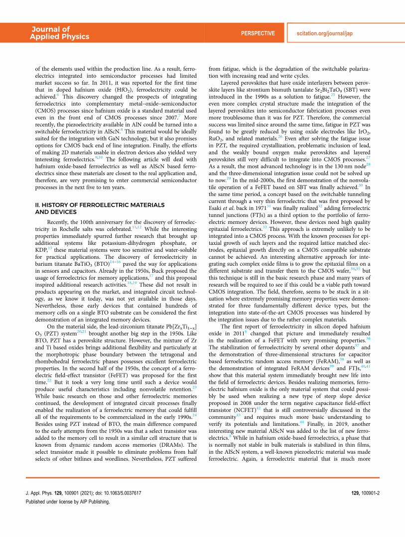
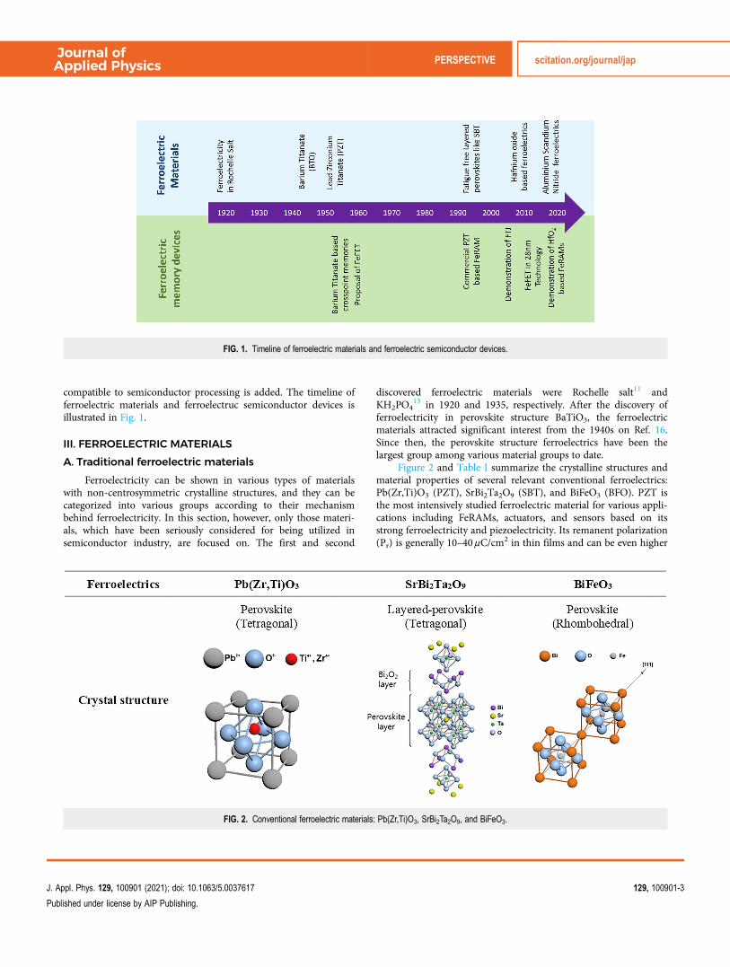
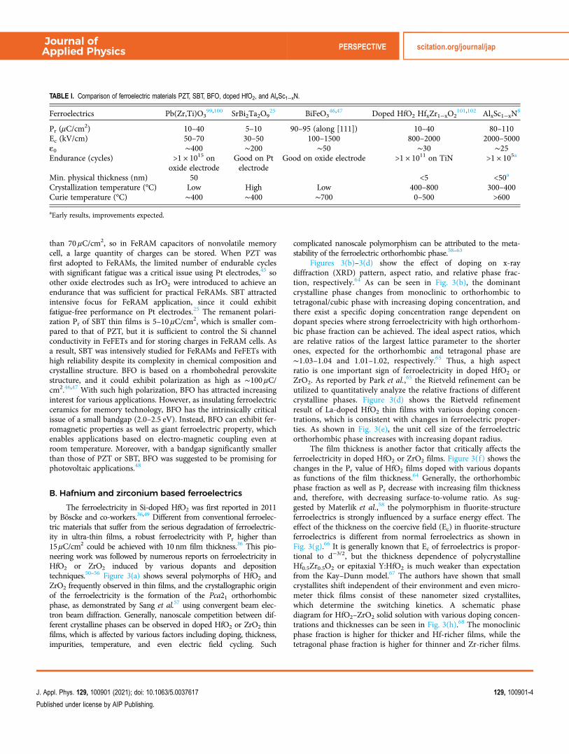
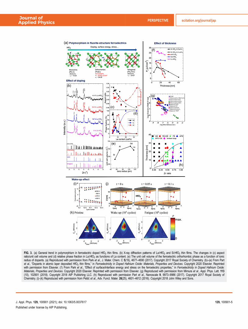

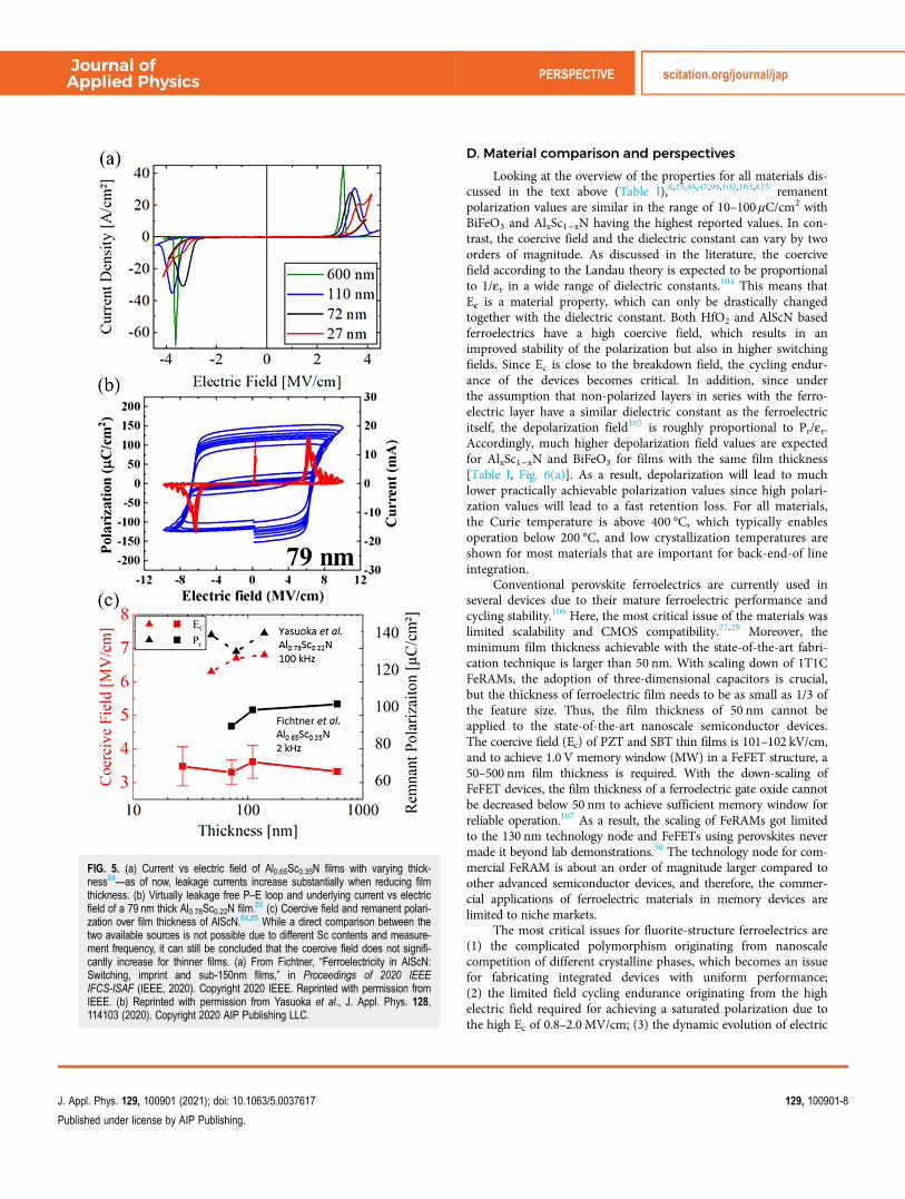
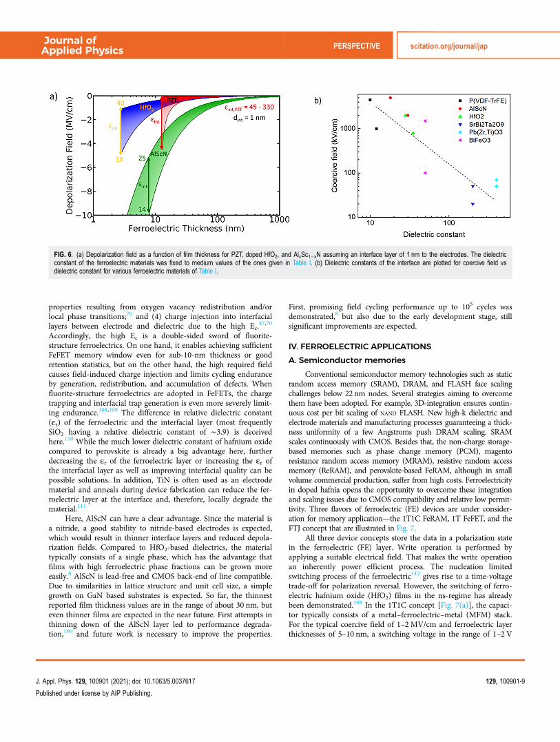
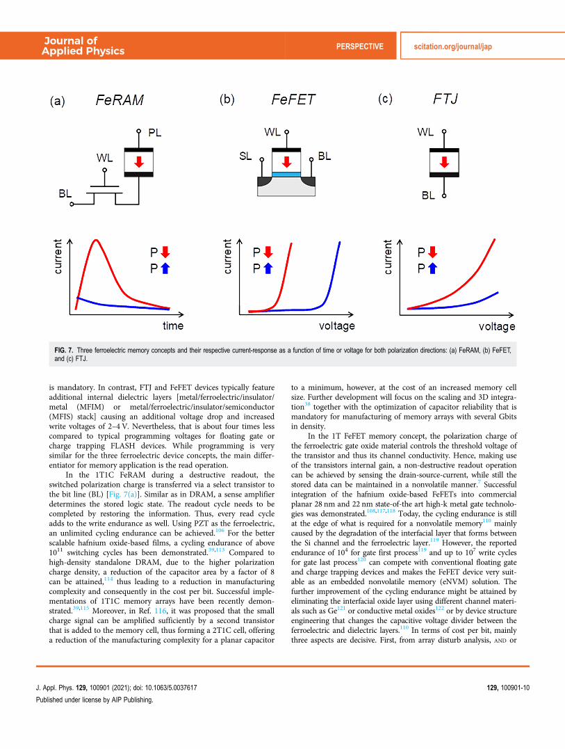
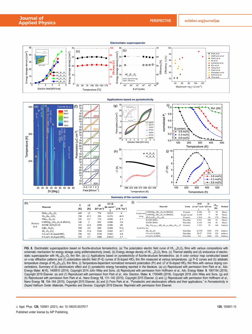


![Sangeetha [Ferroelectric Memory]](https://static.documents.pub/doc/80x56/55cf8f91550346703b9d9665/sangeetha-ferroelectric-memory.jpg)


